EP3406768A1 - Diamant monocristallin, procédé destiné à la fabrication d'un diamant monocristallin, et dispositif de dépôt chimique en phase vapeur associé - Google Patents
Diamant monocristallin, procédé destiné à la fabrication d'un diamant monocristallin, et dispositif de dépôt chimique en phase vapeur associé Download PDFInfo
- Publication number
- EP3406768A1 EP3406768A1 EP17741438.0A EP17741438A EP3406768A1 EP 3406768 A1 EP3406768 A1 EP 3406768A1 EP 17741438 A EP17741438 A EP 17741438A EP 3406768 A1 EP3406768 A1 EP 3406768A1
- Authority
- EP
- European Patent Office
- Prior art keywords
- crystal
- diamond
- principal surface
- points
- crystal diamond
- Prior art date
- Legal status (The legal status is an assumption and is not a legal conclusion. Google has not performed a legal analysis and makes no representation as to the accuracy of the status listed.)
- Granted
Links
Images



Classifications
-
- C—CHEMISTRY; METALLURGY
- C23—COATING METALLIC MATERIAL; COATING MATERIAL WITH METALLIC MATERIAL; CHEMICAL SURFACE TREATMENT; DIFFUSION TREATMENT OF METALLIC MATERIAL; COATING BY VACUUM EVAPORATION, BY SPUTTERING, BY ION IMPLANTATION OR BY CHEMICAL VAPOUR DEPOSITION, IN GENERAL; INHIBITING CORROSION OF METALLIC MATERIAL OR INCRUSTATION IN GENERAL
- C23C—COATING METALLIC MATERIAL; COATING MATERIAL WITH METALLIC MATERIAL; SURFACE TREATMENT OF METALLIC MATERIAL BY DIFFUSION INTO THE SURFACE, BY CHEMICAL CONVERSION OR SUBSTITUTION; COATING BY VACUUM EVAPORATION, BY SPUTTERING, BY ION IMPLANTATION OR BY CHEMICAL VAPOUR DEPOSITION, IN GENERAL
- C23C16/00—Chemical coating by decomposition of gaseous compounds, without leaving reaction products of surface material in the coating, i.e. chemical vapour deposition [CVD] processes
- C23C16/01—Chemical coating by decomposition of gaseous compounds, without leaving reaction products of surface material in the coating, i.e. chemical vapour deposition [CVD] processes on temporary substrates, e.g. substrates subsequently removed by etching
-
- A—HUMAN NECESSITIES
- A44—HABERDASHERY; JEWELLERY
- A44C—PERSONAL ADORNMENTS, e.g. JEWELLERY; COINS
- A44C27/00—Making jewellery or other personal adornments
-
- C—CHEMISTRY; METALLURGY
- C01—INORGANIC CHEMISTRY
- C01B—NON-METALLIC ELEMENTS; COMPOUNDS THEREOF; METALLOIDS OR COMPOUNDS THEREOF NOT COVERED BY SUBCLASS C01C
- C01B32/00—Carbon; Compounds thereof
- C01B32/25—Diamond
- C01B32/26—Preparation
-
- C—CHEMISTRY; METALLURGY
- C23—COATING METALLIC MATERIAL; COATING MATERIAL WITH METALLIC MATERIAL; CHEMICAL SURFACE TREATMENT; DIFFUSION TREATMENT OF METALLIC MATERIAL; COATING BY VACUUM EVAPORATION, BY SPUTTERING, BY ION IMPLANTATION OR BY CHEMICAL VAPOUR DEPOSITION, IN GENERAL; INHIBITING CORROSION OF METALLIC MATERIAL OR INCRUSTATION IN GENERAL
- C23C—COATING METALLIC MATERIAL; COATING MATERIAL WITH METALLIC MATERIAL; SURFACE TREATMENT OF METALLIC MATERIAL BY DIFFUSION INTO THE SURFACE, BY CHEMICAL CONVERSION OR SUBSTITUTION; COATING BY VACUUM EVAPORATION, BY SPUTTERING, BY ION IMPLANTATION OR BY CHEMICAL VAPOUR DEPOSITION, IN GENERAL
- C23C16/00—Chemical coating by decomposition of gaseous compounds, without leaving reaction products of surface material in the coating, i.e. chemical vapour deposition [CVD] processes
- C23C16/02—Pretreatment of the material to be coated
- C23C16/0227—Pretreatment of the material to be coated by cleaning or etching
- C23C16/0236—Pretreatment of the material to be coated by cleaning or etching by etching with a reactive gas
-
- C—CHEMISTRY; METALLURGY
- C23—COATING METALLIC MATERIAL; COATING MATERIAL WITH METALLIC MATERIAL; CHEMICAL SURFACE TREATMENT; DIFFUSION TREATMENT OF METALLIC MATERIAL; COATING BY VACUUM EVAPORATION, BY SPUTTERING, BY ION IMPLANTATION OR BY CHEMICAL VAPOUR DEPOSITION, IN GENERAL; INHIBITING CORROSION OF METALLIC MATERIAL OR INCRUSTATION IN GENERAL
- C23C—COATING METALLIC MATERIAL; COATING MATERIAL WITH METALLIC MATERIAL; SURFACE TREATMENT OF METALLIC MATERIAL BY DIFFUSION INTO THE SURFACE, BY CHEMICAL CONVERSION OR SUBSTITUTION; COATING BY VACUUM EVAPORATION, BY SPUTTERING, BY ION IMPLANTATION OR BY CHEMICAL VAPOUR DEPOSITION, IN GENERAL
- C23C16/00—Chemical coating by decomposition of gaseous compounds, without leaving reaction products of surface material in the coating, i.e. chemical vapour deposition [CVD] processes
- C23C16/22—Chemical coating by decomposition of gaseous compounds, without leaving reaction products of surface material in the coating, i.e. chemical vapour deposition [CVD] processes characterised by the deposition of inorganic material, other than metallic material
- C23C16/26—Deposition of carbon only
- C23C16/27—Diamond only
-
- C—CHEMISTRY; METALLURGY
- C23—COATING METALLIC MATERIAL; COATING MATERIAL WITH METALLIC MATERIAL; CHEMICAL SURFACE TREATMENT; DIFFUSION TREATMENT OF METALLIC MATERIAL; COATING BY VACUUM EVAPORATION, BY SPUTTERING, BY ION IMPLANTATION OR BY CHEMICAL VAPOUR DEPOSITION, IN GENERAL; INHIBITING CORROSION OF METALLIC MATERIAL OR INCRUSTATION IN GENERAL
- C23C—COATING METALLIC MATERIAL; COATING MATERIAL WITH METALLIC MATERIAL; SURFACE TREATMENT OF METALLIC MATERIAL BY DIFFUSION INTO THE SURFACE, BY CHEMICAL CONVERSION OR SUBSTITUTION; COATING BY VACUUM EVAPORATION, BY SPUTTERING, BY ION IMPLANTATION OR BY CHEMICAL VAPOUR DEPOSITION, IN GENERAL
- C23C16/00—Chemical coating by decomposition of gaseous compounds, without leaving reaction products of surface material in the coating, i.e. chemical vapour deposition [CVD] processes
- C23C16/22—Chemical coating by decomposition of gaseous compounds, without leaving reaction products of surface material in the coating, i.e. chemical vapour deposition [CVD] processes characterised by the deposition of inorganic material, other than metallic material
- C23C16/26—Deposition of carbon only
- C23C16/27—Diamond only
- C23C16/274—Diamond only using microwave discharges
-
- C—CHEMISTRY; METALLURGY
- C23—COATING METALLIC MATERIAL; COATING MATERIAL WITH METALLIC MATERIAL; CHEMICAL SURFACE TREATMENT; DIFFUSION TREATMENT OF METALLIC MATERIAL; COATING BY VACUUM EVAPORATION, BY SPUTTERING, BY ION IMPLANTATION OR BY CHEMICAL VAPOUR DEPOSITION, IN GENERAL; INHIBITING CORROSION OF METALLIC MATERIAL OR INCRUSTATION IN GENERAL
- C23C—COATING METALLIC MATERIAL; COATING MATERIAL WITH METALLIC MATERIAL; SURFACE TREATMENT OF METALLIC MATERIAL BY DIFFUSION INTO THE SURFACE, BY CHEMICAL CONVERSION OR SUBSTITUTION; COATING BY VACUUM EVAPORATION, BY SPUTTERING, BY ION IMPLANTATION OR BY CHEMICAL VAPOUR DEPOSITION, IN GENERAL
- C23C16/00—Chemical coating by decomposition of gaseous compounds, without leaving reaction products of surface material in the coating, i.e. chemical vapour deposition [CVD] processes
- C23C16/22—Chemical coating by decomposition of gaseous compounds, without leaving reaction products of surface material in the coating, i.e. chemical vapour deposition [CVD] processes characterised by the deposition of inorganic material, other than metallic material
- C23C16/26—Deposition of carbon only
- C23C16/27—Diamond only
- C23C16/277—Diamond only using other elements in the gas phase besides carbon and hydrogen; using other elements besides carbon, hydrogen and oxygen in case of use of combustion torches; using other elements besides carbon, hydrogen and inert gas in case of use of plasma jets
-
- C—CHEMISTRY; METALLURGY
- C23—COATING METALLIC MATERIAL; COATING MATERIAL WITH METALLIC MATERIAL; CHEMICAL SURFACE TREATMENT; DIFFUSION TREATMENT OF METALLIC MATERIAL; COATING BY VACUUM EVAPORATION, BY SPUTTERING, BY ION IMPLANTATION OR BY CHEMICAL VAPOUR DEPOSITION, IN GENERAL; INHIBITING CORROSION OF METALLIC MATERIAL OR INCRUSTATION IN GENERAL
- C23C—COATING METALLIC MATERIAL; COATING MATERIAL WITH METALLIC MATERIAL; SURFACE TREATMENT OF METALLIC MATERIAL BY DIFFUSION INTO THE SURFACE, BY CHEMICAL CONVERSION OR SUBSTITUTION; COATING BY VACUUM EVAPORATION, BY SPUTTERING, BY ION IMPLANTATION OR BY CHEMICAL VAPOUR DEPOSITION, IN GENERAL
- C23C16/00—Chemical coating by decomposition of gaseous compounds, without leaving reaction products of surface material in the coating, i.e. chemical vapour deposition [CVD] processes
- C23C16/44—Chemical coating by decomposition of gaseous compounds, without leaving reaction products of surface material in the coating, i.e. chemical vapour deposition [CVD] processes characterised by the method of coating
- C23C16/458—Chemical coating by decomposition of gaseous compounds, without leaving reaction products of surface material in the coating, i.e. chemical vapour deposition [CVD] processes characterised by the method of coating characterised by the method used for supporting substrates in the reaction chamber
- C23C16/4581—Chemical coating by decomposition of gaseous compounds, without leaving reaction products of surface material in the coating, i.e. chemical vapour deposition [CVD] processes characterised by the method of coating characterised by the method used for supporting substrates in the reaction chamber characterised by material of construction or surface finish of the means for supporting the substrate
-
- C—CHEMISTRY; METALLURGY
- C30—CRYSTAL GROWTH
- C30B—SINGLE-CRYSTAL GROWTH; UNIDIRECTIONAL SOLIDIFICATION OF EUTECTIC MATERIAL OR UNIDIRECTIONAL DEMIXING OF EUTECTOID MATERIAL; REFINING BY ZONE-MELTING OF MATERIAL; PRODUCTION OF A HOMOGENEOUS POLYCRYSTALLINE MATERIAL WITH DEFINED STRUCTURE; SINGLE CRYSTALS OR HOMOGENEOUS POLYCRYSTALLINE MATERIAL WITH DEFINED STRUCTURE; AFTER-TREATMENT OF SINGLE CRYSTALS OR A HOMOGENEOUS POLYCRYSTALLINE MATERIAL WITH DEFINED STRUCTURE; APPARATUS THEREFOR
- C30B25/00—Single-crystal growth by chemical reaction of reactive gases, e.g. chemical vapour-deposition growth
- C30B25/02—Epitaxial-layer growth
- C30B25/08—Reaction chambers; Selection of materials therefor
-
- C—CHEMISTRY; METALLURGY
- C30—CRYSTAL GROWTH
- C30B—SINGLE-CRYSTAL GROWTH; UNIDIRECTIONAL SOLIDIFICATION OF EUTECTIC MATERIAL OR UNIDIRECTIONAL DEMIXING OF EUTECTOID MATERIAL; REFINING BY ZONE-MELTING OF MATERIAL; PRODUCTION OF A HOMOGENEOUS POLYCRYSTALLINE MATERIAL WITH DEFINED STRUCTURE; SINGLE CRYSTALS OR HOMOGENEOUS POLYCRYSTALLINE MATERIAL WITH DEFINED STRUCTURE; AFTER-TREATMENT OF SINGLE CRYSTALS OR A HOMOGENEOUS POLYCRYSTALLINE MATERIAL WITH DEFINED STRUCTURE; APPARATUS THEREFOR
- C30B25/00—Single-crystal growth by chemical reaction of reactive gases, e.g. chemical vapour-deposition growth
- C30B25/02—Epitaxial-layer growth
- C30B25/12—Substrate holders or susceptors
-
- C—CHEMISTRY; METALLURGY
- C30—CRYSTAL GROWTH
- C30B—SINGLE-CRYSTAL GROWTH; UNIDIRECTIONAL SOLIDIFICATION OF EUTECTIC MATERIAL OR UNIDIRECTIONAL DEMIXING OF EUTECTOID MATERIAL; REFINING BY ZONE-MELTING OF MATERIAL; PRODUCTION OF A HOMOGENEOUS POLYCRYSTALLINE MATERIAL WITH DEFINED STRUCTURE; SINGLE CRYSTALS OR HOMOGENEOUS POLYCRYSTALLINE MATERIAL WITH DEFINED STRUCTURE; AFTER-TREATMENT OF SINGLE CRYSTALS OR A HOMOGENEOUS POLYCRYSTALLINE MATERIAL WITH DEFINED STRUCTURE; APPARATUS THEREFOR
- C30B25/00—Single-crystal growth by chemical reaction of reactive gases, e.g. chemical vapour-deposition growth
- C30B25/02—Epitaxial-layer growth
- C30B25/18—Epitaxial-layer growth characterised by the substrate
- C30B25/186—Epitaxial-layer growth characterised by the substrate being specially pre-treated by, e.g. chemical or physical means
-
- C—CHEMISTRY; METALLURGY
- C30—CRYSTAL GROWTH
- C30B—SINGLE-CRYSTAL GROWTH; UNIDIRECTIONAL SOLIDIFICATION OF EUTECTIC MATERIAL OR UNIDIRECTIONAL DEMIXING OF EUTECTOID MATERIAL; REFINING BY ZONE-MELTING OF MATERIAL; PRODUCTION OF A HOMOGENEOUS POLYCRYSTALLINE MATERIAL WITH DEFINED STRUCTURE; SINGLE CRYSTALS OR HOMOGENEOUS POLYCRYSTALLINE MATERIAL WITH DEFINED STRUCTURE; AFTER-TREATMENT OF SINGLE CRYSTALS OR A HOMOGENEOUS POLYCRYSTALLINE MATERIAL WITH DEFINED STRUCTURE; APPARATUS THEREFOR
- C30B25/00—Single-crystal growth by chemical reaction of reactive gases, e.g. chemical vapour-deposition growth
- C30B25/02—Epitaxial-layer growth
- C30B25/18—Epitaxial-layer growth characterised by the substrate
- C30B25/20—Epitaxial-layer growth characterised by the substrate the substrate being of the same materials as the epitaxial layer
-
- C—CHEMISTRY; METALLURGY
- C30—CRYSTAL GROWTH
- C30B—SINGLE-CRYSTAL GROWTH; UNIDIRECTIONAL SOLIDIFICATION OF EUTECTIC MATERIAL OR UNIDIRECTIONAL DEMIXING OF EUTECTOID MATERIAL; REFINING BY ZONE-MELTING OF MATERIAL; PRODUCTION OF A HOMOGENEOUS POLYCRYSTALLINE MATERIAL WITH DEFINED STRUCTURE; SINGLE CRYSTALS OR HOMOGENEOUS POLYCRYSTALLINE MATERIAL WITH DEFINED STRUCTURE; AFTER-TREATMENT OF SINGLE CRYSTALS OR A HOMOGENEOUS POLYCRYSTALLINE MATERIAL WITH DEFINED STRUCTURE; APPARATUS THEREFOR
- C30B25/00—Single-crystal growth by chemical reaction of reactive gases, e.g. chemical vapour-deposition growth
- C30B25/02—Epitaxial-layer growth
- C30B25/18—Epitaxial-layer growth characterised by the substrate
- C30B25/20—Epitaxial-layer growth characterised by the substrate the substrate being of the same materials as the epitaxial layer
- C30B25/205—Epitaxial-layer growth characterised by the substrate the substrate being of the same materials as the epitaxial layer the substrate being of insulating material
-
- C—CHEMISTRY; METALLURGY
- C30—CRYSTAL GROWTH
- C30B—SINGLE-CRYSTAL GROWTH; UNIDIRECTIONAL SOLIDIFICATION OF EUTECTIC MATERIAL OR UNIDIRECTIONAL DEMIXING OF EUTECTOID MATERIAL; REFINING BY ZONE-MELTING OF MATERIAL; PRODUCTION OF A HOMOGENEOUS POLYCRYSTALLINE MATERIAL WITH DEFINED STRUCTURE; SINGLE CRYSTALS OR HOMOGENEOUS POLYCRYSTALLINE MATERIAL WITH DEFINED STRUCTURE; AFTER-TREATMENT OF SINGLE CRYSTALS OR A HOMOGENEOUS POLYCRYSTALLINE MATERIAL WITH DEFINED STRUCTURE; APPARATUS THEREFOR
- C30B29/00—Single crystals or homogeneous polycrystalline material with defined structure characterised by the material or by their shape
- C30B29/02—Elements
- C30B29/04—Diamond
-
- H—ELECTRICITY
- H10—SEMICONDUCTOR DEVICES; ELECTRIC SOLID-STATE DEVICES NOT OTHERWISE PROVIDED FOR
- H10P—GENERIC PROCESSES OR APPARATUS FOR THE MANUFACTURE OR TREATMENT OF DEVICES COVERED BY CLASS H10
- H10P14/00—Formation of materials, e.g. in the shape of layers or pillars
- H10P14/20—Formation of materials, e.g. in the shape of layers or pillars of semiconductor materials
- H10P14/24—Formation of materials, e.g. in the shape of layers or pillars of semiconductor materials using chemical vapour deposition [CVD]
-
- H—ELECTRICITY
- H10—SEMICONDUCTOR DEVICES; ELECTRIC SOLID-STATE DEVICES NOT OTHERWISE PROVIDED FOR
- H10P—GENERIC PROCESSES OR APPARATUS FOR THE MANUFACTURE OR TREATMENT OF DEVICES COVERED BY CLASS H10
- H10P14/00—Formation of materials, e.g. in the shape of layers or pillars
- H10P14/20—Formation of materials, e.g. in the shape of layers or pillars of semiconductor materials
- H10P14/29—Formation of materials, e.g. in the shape of layers or pillars of semiconductor materials characterised by the substrates
- H10P14/2901—Materials
- H10P14/2902—Materials being Group IVA materials
- H10P14/2903—Carbon, e.g. diamond-like carbon
-
- H—ELECTRICITY
- H10—SEMICONDUCTOR DEVICES; ELECTRIC SOLID-STATE DEVICES NOT OTHERWISE PROVIDED FOR
- H10P—GENERIC PROCESSES OR APPARATUS FOR THE MANUFACTURE OR TREATMENT OF DEVICES COVERED BY CLASS H10
- H10P14/00—Formation of materials, e.g. in the shape of layers or pillars
- H10P14/20—Formation of materials, e.g. in the shape of layers or pillars of semiconductor materials
- H10P14/29—Formation of materials, e.g. in the shape of layers or pillars of semiconductor materials characterised by the substrates
- H10P14/2926—Crystal orientations
-
- H—ELECTRICITY
- H10—SEMICONDUCTOR DEVICES; ELECTRIC SOLID-STATE DEVICES NOT OTHERWISE PROVIDED FOR
- H10P—GENERIC PROCESSES OR APPARATUS FOR THE MANUFACTURE OR TREATMENT OF DEVICES COVERED BY CLASS H10
- H10P14/00—Formation of materials, e.g. in the shape of layers or pillars
- H10P14/20—Formation of materials, e.g. in the shape of layers or pillars of semiconductor materials
- H10P14/34—Deposited materials, e.g. layers
- H10P14/3402—Deposited materials, e.g. layers characterised by the chemical composition
- H10P14/3404—Deposited materials, e.g. layers characterised by the chemical composition being Group IVA materials
- H10P14/3406—Carbon, e.g. diamond-like carbon
-
- H—ELECTRICITY
- H10—SEMICONDUCTOR DEVICES; ELECTRIC SOLID-STATE DEVICES NOT OTHERWISE PROVIDED FOR
- H10P—GENERIC PROCESSES OR APPARATUS FOR THE MANUFACTURE OR TREATMENT OF DEVICES COVERED BY CLASS H10
- H10P14/00—Formation of materials, e.g. in the shape of layers or pillars
- H10P14/20—Formation of materials, e.g. in the shape of layers or pillars of semiconductor materials
- H10P14/34—Deposited materials, e.g. layers
- H10P14/3451—Structure
- H10P14/3452—Microstructure
- H10P14/3456—Polycrystalline
-
- H—ELECTRICITY
- H10—SEMICONDUCTOR DEVICES; ELECTRIC SOLID-STATE DEVICES NOT OTHERWISE PROVIDED FOR
- H10P—GENERIC PROCESSES OR APPARATUS FOR THE MANUFACTURE OR TREATMENT OF DEVICES COVERED BY CLASS H10
- H10P14/00—Formation of materials, e.g. in the shape of layers or pillars
- H10P14/20—Formation of materials, e.g. in the shape of layers or pillars of semiconductor materials
- H10P14/36—Formation of materials, e.g. in the shape of layers or pillars of semiconductor materials characterised by treatments done before the formation of the materials
-
- H—ELECTRICITY
- H10—SEMICONDUCTOR DEVICES; ELECTRIC SOLID-STATE DEVICES NOT OTHERWISE PROVIDED FOR
- H10P—GENERIC PROCESSES OR APPARATUS FOR THE MANUFACTURE OR TREATMENT OF DEVICES COVERED BY CLASS H10
- H10P14/00—Formation of materials, e.g. in the shape of layers or pillars
- H10P14/20—Formation of materials, e.g. in the shape of layers or pillars of semiconductor materials
- H10P14/38—Formation of materials, e.g. in the shape of layers or pillars of semiconductor materials characterised by treatments done after the formation of the materials
Definitions
- the present invention relates to a single-crystal diamond, a method for manufacturing a single-crystal diamond, and a chemical vapor deposition device used in the method.
- the present application claims priority based on Japanese Patent Application No. 2016-010560 filed on January 22, 2016 .
- the disclosure of the Japanese patent application is incorporated herein by reference in its entirety.
- Diamonds have excellent characteristics such as high light transmissivity, high thermal conductivity, high carrier mobility, high dielectric breakdown electric field and low inductive loss, and are widely used for cutting tools and abrasion-proof tools particularly because of its unusually high hardness.
- a natural single-crystal diamond or a single-crystal diamond synthesized by a high-temperature and high-pressure method has been widely used, but in recent years, it has been possible to synthesize a thick and self-standing single-crystal diamond even by a chemical vapor deposition method, and application of such a single-crystal diamond in various fields as described above has been expected.
- PTD 1 discloses a method in which the density of defects on a surface of a diamond base as a seed substrate is reduced, and a diamond is then synthesized by a CVD method for obtaining a CVD single-crystal diamond having light transmissivity and excellent electronic physical properties with regard to a high-quality CVD single-crystal diamond layer having a thickness greater than 2 mm, and a method for production thereof.
- a method for manufacturing a single-crystal diamond according to one aspect of the present invention includes the steps of: forming a protective film on at least a part of a surface of an auxiliary plate; preparing a diamond seed crystal substrate; disposing an auxiliary plate with a protective film that has the protective film formed on the auxiliary plate, and the diamond seed crystal substrate in a chamber; and growing a single-crystal diamond on a principal surface of the diamond seed crystal substrate by a chemical vapor deposition method while introducing a carbon-containing gas into the chamber.
- a single-crystal diamond according to one aspect of the present invention contains nitrogen as an impurity element in an amount of less than 500 ppb.
- a single-crystal diamond according to one aspect of the present invention contains silicon as an impurity element in an amount of less than 1000 ppb.
- a single-crystal diamond according to one aspect of the present invention contains impurity elements other than nitrogen and silicon in an amount of less than 500 ppb.
- a chemical vapor deposition device is a chemical vapor deposition device to be used in the method for manufacturing a single-crystal diamond according to the above-mentioned aspect, the device including the chamber, and the auxiliary plate with the protective film, the auxiliary plate with the protective film being disposed in the chamber and having the protective film formed on at least a part of a surface of the auxiliary plate.
- PTD 1 2004-503461
- the cutting tool, abrasion-proof or the like has a short lifetime because such a CVD single-crystal diamond has lower chipping resistance, and is more easily chipped as compared to a natural single-crystal diamond, and a single-crystal diamond grown by a high-temperature and high-pressure method (hereinafter, also referred to as a high-temperature and high-pressure single-crystal diamond).
- impurity elements in the CVD single-crystal diamond are mixed in a cut material and/or a polished material.
- an object of the present disclosure is to solve the above-mentioned problems and to provide a single-crystal diamond which is suitably used for semiconductor materials (diodes, transistors and the like), electronic components (resistive parts, capacitive parts and the like), heat dissipation materials (heat sinks), optical components (window materials, lenses and the like), ornament materials, cutting tools, polishing tools and the like and which has a high purity, high light transmissivity and excellent chipping resistance, a method for manufacturing a single-crystal diamond, and a chemical vapor deposition device used in the method.
- a single-crystal diamond having a high purity, high light transmissivity and excellent chipping resistance it is possible to provide a single-crystal diamond having a high purity, high light transmissivity and excellent chipping resistance, a method for manufacturing a single-crystal diamond, and a chemical vapor deposition device used in the method.
- a single-crystal diamond which is suitably used for semiconductor materials (diodes, transistors and the like), electronic components (resistive parts, capacitive parts and the like), heat dissipation materials (heat sinks), optical components (window materials, lenses and the like), ornament materials, cutting tools, polishing tools and the like, a method for manufacturing a single-crystal diamond, and a chemical vapor deposition device used in the method.
- a method for manufacturing a single-crystal diamond according to one embodiment of the present invention includes the steps of: forming a protective film on at least a part of a surface of an auxiliary plate; preparing a diamond seed crystal substrate; disposing an auxiliary plate with a protective film that has the protective film formed on the auxiliary plate, and a diamond seed crystal substrate in a chamber; and growing a single-crystal diamond on a principal surface of the diamond seed crystal substrate by a chemical vapor deposition method while introducing a carbon-containing gas into the chamber.
- a single-crystal diamond having a low content of impurity elements, high light transmissivity and excellent chipping resistance can be obtained because the method includes the above-mentioned steps.
- the auxiliary plate can be formed of an oxide.
- the single-crystal diamond can be further stably and efficiently obtained because the auxiliary plate transmits a microwave, and is stable even under a reducing atmosphere.
- the protective film may contain a metal element serving as a getter of an element other than carbon.
- the getter adsorbs impurity elements in the chamber to prevent ingress of the impurity elements into the single-crystal diamond, and thus a single-crystal diamond having a further low content of impurity elements can be obtained.
- the step of preparing a diamond seed crystal substrate may be a step of preparing a diamond seed crystal substrate having a seed crystal damage point on a principal surface.
- the step of preparing a diamond seed crystal substrate may be a step of preparing a diamond seed substrate in which groups of crystal defect points aggregate on a principal surface by a CVD method.
- the single-crystal diamond can be obtained in which groups of crystal defect points that are tip points at which crystal defect lines reach a crystal growth principal surface aggregate.
- the single-crystal diamond stress is relaxed by a large number of crystal defect lines to suppress occurrence of large chipping, and chipping can be made hard to occur by regions where groups of crystal defect points aggregate. Therefore, the single-crystal diamond is suitably used for semiconductor materials (diodes, transistors and the like), electronic components (resistive parts, capacitive parts and the like), heat dissipation materials (heat sinks), optical components (window materials, lenses and the like), ornament materials, cutting tools, polishing tools and the like.
- the step of preparing a diamond seed crystal substrate may be a step of preparing a diamond seed crystal substrate having on a principal surface a seed crystal defect linear aggregation region where groups of seed crystal defect points aggregate and extend linearly.
- the single-crystal diamond can be obtained in which a plurality of crystal defect linear aggregation regions, where groups of crystal defect points that are tip points at which crystal defect lines reach a crystal growth principal surface aggregate and extend linearly in a direction at an angle less than or equal to 30° with respect to one arbitrarily specified direction, are present in parallel.
- the single-crystal diamond stress is relaxed by a large number of crystal defect lines to suppress occurrence of large chipping, and a direction in which chipping hardly occurs can be controlled by a plurality of crystal defect linear aggregation regions which are present in parallel, and extend linearly in a direction at an angle less than or equal to 30° with respect to one arbitrarily specified direction. Therefore, the single-crystal diamond is suitably used for semiconductor materials (diodes, transistors and the like), electronic components (resistive parts, capacitive parts and the like), heat dissipation materials (heat sinks), optical components (window materials, lenses and the like), ornament materials, cutting tools, polishing tools and the like.
- two or more seed crystal defect linear aggregation regions may be present per 1 mm in a direction perpendicular to a direction in which the seed crystal defect linear aggregation regions extend linearly, and the distance between the seed crystal defect linear aggregation regions may be less than or equal to 500 ⁇ m in the direction in which the regions extend linearly.
- the direction in which the seed crystal defect linear aggregation region extends linearly refers to the specified one direction which is an average direction in a plurality of directions in which a plurality of seed crystal defect linear aggregation regions extend respectively.
- two or more seed crystal defect linear aggregation regions are present per 1 mm in a direction perpendicular to a direction in which the seed crystal defect linear aggregation regions extend linearly, and the distance between the seed crystal defect linear aggregation regions is less than or equal to 500 ⁇ m in the direction in which the regions extend linearly.
- a single-crystal diamond in which two or more seed crystal defect linear aggregation regions are present per 1 mm in a direction perpendicular to a direction in which the crystal defect linear aggregation regions extend linearly, and the distance between the crystal defect linear aggregation regions is less than or equal to 500 ⁇ m in the direction in which the regions extend linearly can be obtained by a chemical vapor deposition method.
- the single-crystal diamond can be obtained in which stress is relaxed by a large number of crystal defect lines to suppress occurrence of large chipping, and a direction in which chipping hardly occurs can be controlled by a plurality of dense crystal defect linear aggregation regions which are present in parallel, and extend linearly in a direction at an angle less than or equal to 30° with respect to one arbitrarily specified direction.
- the method for manufacturing a single-crystal diamond in the method for manufacturing a single-crystal diamond according to this embodiment, five or more long seed crystal defect linear aggregation regions having a length greater than or equal to 300 ⁇ m may be present per 1 cm 2 of the principal surface.
- occurrence of large chipping in a single-crystal diamond to be grown is suppressed, and the strength of the single-crystal diamond as a whole is increased because five or more long seed crystal defect linear aggregation regions having a length greater than or equal to 300 ⁇ m are present per 1 cm 2 of the principal surface.
- twenty or more longer seed crystal defect linear aggregation regions having a length greater than or equal to 500 ⁇ m may be present per 1 cm 2 of the principal surface.
- the density of seed crystal defect points may be greater than 10 mm -2 .
- the density of seed crystal defect points is greater than 10 mm -2 , and thus a single-crystal diamond in which the density of crystal defect points that are tip points at which the crystal defect lines reach the crystal growth principal surface is greater than 20 mm -2 can be obtained by a chemical vapor deposition method. Therefore, a single-crystal diamond can be obtained in which stress is relaxed by dense crystal defect lines to suppress occurrence of large chipping.
- the density of seed crystal defect points may be greater than 100 mm -2 .
- the density of seed crystal defect points is greater than 100 mm -2 , and thus a single-crystal diamond in which the density of crystal defect points that are tip points at which the crystal defect lines reach the crystal growth principal surface is greater than 300 mm -2 can be obtained by a chemical vapor deposition method. Therefore, a single-crystal diamond can be obtained in which stress is relaxed by dense crystal defect lines to further suppress occurrence of large chipping. Further, from the viewpoint of further suppressing large chipping in a single-crystal diamond, the density of seed crystal defect points may be greater than 1000 mm -2 , or greater than 1 ⁇ 10 4 mm -2 .
- the density of seed crystal defect points may be preferably 1 ⁇ 10 6 mm -2 .
- the density of complex dislocation points that are tip points at which complex dislocations obtained by combining a plurality of edge dislocations and/or a plurality of helical dislocations reach a crystal growth principal surface, among crystal defect points of a single-crystal diamond to be grown may be greater than 20 mm -2 .
- the density of complex dislocation points that are tip points at which complex dislocations reach a crystal growth principal surface is greater than 20 mm -2 , and the effect of relaxing stress by complex dislocations is high.
- the density of complex dislocation points may be preferably greater than 30 mm -2 , more preferably greater than 300 cm -2 .
- the density of seed crystal damage points indicating points at which crystal damage is present may be greater than 3 mm -2 in a secondary electron image in an electron microscope after a principal surface of a diamond seed crystal substrate is hydrogen-terminated.
- the density of seed crystal damage points that generate a large number of crystal defect lines particularly in a single-crystal diamond grown by a chemical vapor deposition method, among seed defect points is greater than 3 mm -2 , and thus a single-crystal diamond having dense crystal defect lines can be obtained by a chemical vapor deposition method. Therefore, a single-crystal diamond can be obtained in which stress is relaxed by dense crystal defect lines to suppress large chipping.
- a single-crystal diamond which has a high light transmittance and in which groups of crystal defect points that are tip points at which crystal defect lines indicating lines having crystal defects in an X-ray topographic image for a crystal growth principal surface reach the crystal growth principal surface aggregate.
- a single-crystal diamond according to one embodiment of the present invention contains nitrogen as an impurity element in an amount of less than 500 ppb. Since the single-crystal diamond contains nitrogen atoms as impurity element atoms only in an amount of less than 500 ppb, the single-crystal diamond has a high purity and high light transmittance, and has a low concentration of nitrogen atoms as heterogeneous element atoms that disturb extension of chipping in application of strong stress to a specific portion, and therefore large chipping over a long distance easily occurs, but since a large number of crystal defect lines themselves, and relaxation of stress by the crystal defect lines disturb extension of chipping, occurrence of large chipping is suppressed.
- the single-crystal diamond of this embodiment which contains nitrogen atoms as impurity element atoms in an amount of less than 500 ppb is suitably used for applications of semiconductor materials (diodes, transistors and the like), electronic components (resistive parts, capacitive parts and the like), heat dissipation materials (heat sinks), optical components (window materials, lenses and the like), ornament materials, cutting tools, polishing tools and the like.
- the single-crystal diamond of this embodiment may contain nitrogen atoms as impurity element atoms in an amount of less than 250 ppb, in an amount of less than 75 ppb, in an amount of less than 35 ppb, or in an amount of less than 15 ppb.
- the single-crystal diamond may contain nitrogen atoms preferably in an amount of greater than or equal to 0.05 ppb.
- the impurity element means an element (heterogeneous element) other than carbon which is a principal constituent element of the single-crystal diamond.
- a single-crystal diamond according to one embodiment of the present invention contains silicon as an impurity element in an amount of less than 1000 ppb. Since the single-crystal diamond contains silicon atoms as impurity element atoms only in an amount of less than 1000 ppb, the single-crystal diamond has a high purity and high light transmittance, and has a low concentration of silicon atoms as heterogeneous element atoms that disturb extension of chipping in application of strong stress to a specific portion, and therefore large chipping over a long distance easily occurs, but since a large number of crystal defect lines themselves, and relaxation of stress by the crystal defect lines disturb extension of chipping, occurrence of large chipping is suppressed.
- the single-crystal diamond of this embodiment which contains silicon atoms as impurity element atoms in an amount of less than 1000 ppb is suitably used for applications of semiconductor materials (diodes, transistors and the like), electronic components (resistive parts, capacitive parts and the like), heat dissipation materials (heat sinks), optical components (window materials, lenses and the like), ornament materials, cutting tools, polishing tools and the like.
- the single-crystal diamond of this embodiment may contain silicon atoms as impurity element atoms in an amount of less than 200 ppb, in an amount of less than 50 ppb, in an amount of less than 5 ppb, in an amount of less than 0.5 ppb, in an amount of less than 0.05 ppb, or in an amount of less than 0.005 ppb.
- the single-crystal diamond may contain silicon atoms preferably in an amount of greater than or equal to 0.0005 ppb.
- a single-crystal diamond according to one embodiment of the present invention contains impurity elements other than nitrogen and silicon in an amount of less than 500 ppb. Since the single-crystal diamond contains impurity element atoms other than nitrogen atoms and silicon atoms only in an amount of less than 500 ppb, the single-crystal diamond has a high purity and high light transmittance, and has a low concentration of impurity element atoms other than nitrogen atoms and silicon atoms, which are heterogeneous element atoms that disturb extension of chipping in application of strong stress to a specific portion, and therefore large chipping over a long distance easily occurs, but since a large number of crystal defect lines themselves, and relaxation of stress by the crystal defect lines disturb extension of chipping, occurrence of large chipping is suppressed.
- the single-crystal diamond of this embodiment which contains impurity element atoms other than nitrogen atoms and silicon atoms as impurity element atoms in an amount of less than 500 ppb is suitably used for applications of semiconductor materials (diodes, transistors and the like), electronic components (resistive parts, capacitive parts and the like), heat dissipation materials (heat sinks), optical components (window materials, lenses and the like), ornament materials, cutting tools, polishing tools and the like.
- semiconductor materials diodes, transistors and the like
- electronic components resistive parts, capacitive parts and the like
- heat dissipation materials heat sinks
- optical components windshield materials, lenses and the like
- ornament materials ornament materials, cutting tools, polishing tools and the like.
- the single-crystal diamond of this embodiment may contain impurity element atoms other than nitrogen atoms and silicon atoms in an amount of less than 200 ppb, in an amount of less than 100 ppb, or in an amount of less than 75 ppb.
- the single-crystal diamond may contain impurity element atoms other than nitrogen atoms and silicon atoms preferably in an amount of greater than or equal to 1 ppb.
- the transmittance of light having a wavelength of 500 nm may be greater than or equal to 55% and less than 71% when the single-crystal diamond has a thickness of 500 ⁇ m.
- the light transmittance when the single-crystal diamond has a thickness of 500 ⁇ m is a light transmittance measured when the single-crystal diamond has a thickness of 500 ⁇ m, or a light transmittance determined by measuring a light transmittance when the thickness of the single-crystal diamond is not 500 ⁇ m, and converting the measured light transmittance to a value when the single-crystal diamond has a thickness of 500 ⁇ m.
- the light transmittance means a regular transmittance with conversion performed for correcting surface scattering.
- a conventional single-crystal diamond absorbs light having a wavelength of 500 nm due to a synergistic effect of crystal defects and impurity element atoms, so that the transmittance of light having such a wavelength decreases.
- the single-crystal diamond of this embodiment has a high purity, the single-crystal diamond has a high light transmittance, and occurrence of large chipping is suppressed while the transmittance of light having a wavelength of 500 nm is greater than or equal to 55% when the thickness is 500 ⁇ m.
- the light transmittance is preferably greater than or equal to 55%, more preferably greater than or equal to 60%, still preferably greater than or equal to 65%, especially preferably greater than or equal to 68%. Even in an ideal single-crystal diamond with impurities reduced to a limit, the light transmittance is less than 71%.
- groups of crystal defect points that are tip points at which crystal defect lines indicating lines having crystal defects in an X-ray topographic image for a crystal growth principal surface reach the crystal growth principal surface may aggregate.
- the single-crystal diamond is suitably used for cutting tools, polishing tools, optical components, electronic components, semiconductor materials and the like because the single-crystal diamond has a high purity and a high light transmittance, and stress is relaxed by a large number of crystal defect lines to suppress occurrence of large chipping.
- a plurality of crystal defect linear aggregation regions where groups of crystal defect points that are tip points at which crystal defect lines indicating lines having crystal defects in an X-ray topographic image for a crystal growth principal surface reach the crystal growth principal surface aggregate and extend linearly in a direction at an angle less than or equal to 30° with respect to one arbitrarily specified direction, may be present in parallel.
- the single-crystal diamond has a high purity and high light transmittance, and a plurality of crystal defect linear aggregation regions, where groups of crystal defect points that are tip points at which crystal defect lines reach the crystal growth principal surface aggregate and extend linearly in a direction at an angle less than or equal to 30° with respect to one arbitrarily specified direction, are present in parallel, stress is relaxed by a large number of crystal defect lines to suppress occurrence of large chipping, and a direction in which chipping hardly occurs can be controlled by a plurality of crystal defect linear aggregation regions which are present in parallel, and extend linearly in a direction at an angle less than or equal to 30° with respect to one arbitrarily specified direction. Therefore, the single-crystal diamond is suitably used for cutting tools, polishing tools, optical components, electronic components, semiconductor materials and the like.
- two or more crystal defect linear aggregation regions may be present per 1 mm in a direction perpendicular to a direction in which the crystal defect linear aggregation regions extend linearly, and the distance between the crystal defect linear aggregation regions may be less than or equal to 500 ⁇ m in the direction in which the regions extend linearly.
- the direction in which the crystal defect linear aggregation region extends linearly refers to the specified one direction which is an average direction in a plurality of directions in which a plurality of crystal defect linear aggregation regions extend respectively.
- the single-crystal diamond has a high purity and high light transmittance, two or more crystal defect linear aggregation regions are present per 1 mm in a direction perpendicular to a direction in which the crystal defect linear aggregation regions extend linearly, and the distance between the crystal defect linear aggregation regions is less than or equal to 500 ⁇ m in the direction in which the regions extend linearly, stress is relaxed by a large number of crystal defect lines to suppress occurrence of large chipping, and a direction in which chipping hardly occurs can be controlled by a plurality of dense crystal defect linear aggregation regions which are present in parallel in a direction at an angle less than or equal to 30° with respect to one arbitrarily specified direction.
- the single-crystal diamond of this embodiment five or more long crystal defect linear aggregation regions having a length greater than or equal to 300 ⁇ m may be present per 1 cm 2 of the crystal growth principal surface. Since the single-crystal diamond has a high purity and high light transmittance, and five or more long crystal defect linear aggregation regions having a length greater than or equal to 300 ⁇ m are present per 1 cm 2 of the crystal growth principal surface, occurrence of large chipping in a single-crystal diamond is suppressed, and the strength of the single-crystal diamond as a whole is increased. From such a viewpoint, twenty or more longer crystal defect linear aggregation regions having a length greater than or equal to 500 ⁇ m may be present per 1 cm 2 of the principal surface.
- the density of crystal defect points may be greater than 20 mm -2 . Since the single-crystal diamond has a high purity and high light transmittance, and the density of crystal defect points is greater than 20 mm -2 , occurrence of large chipping is suppressed due to relaxation of stress by dense crystal defect lines corresponding to dense crystal defect points. Further, in the single-crystal diamond of this embodiment, the density of crystal defect points may be greater than 300 mm -2 . In the single-crystal diamond, occurrence of large chipping is further suppressed due to relaxation of stress by dense crystal defect lines corresponding to denser crystal defect points because the density of crystal defect points is greater than 300 mm -2 .
- the density of crystal defect points may be greater than 1500 mm -2 .
- occurrence of large chipping is further suppressed due to relaxation of stress by dense crystal defect lines corresponding to further dense crystal defect points because the density of crystal defect points is greater than 1500 mm -2 .
- the density of complex dislocation points that are tip points at which complex dislocations obtained by combining any of a plurality of edge dislocations and a plurality of helical dislocations reach a crystal growth principal surface, among crystal defect points may be greater than 20 mm -2 . Since the single-crystal diamond has a high purity and high light transmittance, the density of complex dislocation points that are tip points at which complex dislocations reach a crystal growth principal surface is greater than 20 mm -2 , and the effect of relaxing stress by complex dislocations is high, occurrence of large chipping is further suppressed.
- the density of complex dislocation points that are tip points at which complex dislocations obtained by combining any of a plurality of edge dislocations and a plurality of helical dislocations reach a crystal growth principal surface, among crystal defect points may be greater than 30 mm -2 .
- occurrence of large chipping is still further suppressed because the density of complex dislocation points that are tip points at which complex dislocations reach a crystal growth principal surface is greater than 30 mm -2 , and the effect of relaxing stress by complex dislocations is higher.
- the density of complex dislocation points that are tip points at which complex dislocations obtained by combining any of a plurality of edge dislocations and a plurality of helical dislocations reach a crystal growth principal surface, among crystal defect points may be greater than 500 mm -2 .
- occurrence of large chipping is still further suppressed because the density of complex dislocation points that are tip points at which complex dislocations reach a crystal growth principal surface is greater than 500 mm -2 , and the effect of relaxing stress by complex dislocations is higher.
- the density of complex dislocation points that are tip points at which complex dislocations obtained by combining any of a plurality of edge dislocations and a plurality of helical dislocations reach a crystal growth principal surface, among crystal defect points may be greater than 1000 mm -2 .
- occurrence of large chipping is still further suppressed because the density of complex dislocation points that are tip points at which complex dislocations reach a crystal growth principal surface is greater than 1000 mm -2 , and the effect of relaxing stress by complex dislocations is higher.
- the single-crystal diamond of this embodiment may include a plurality of single-crystal diamond layers. Since the single-crystal diamond has a high purity and high light transmittance, and includes a plurality of single-crystal diamond layers, formation of crystal defect lines is accelerated, so that occurrence of large chipping is further suppressed.
- the single-crystal diamond of this embodiment includes a plurality of single-crystal diamond layers, crystal defect lines are newly generated or branched at interfaces between the single-crystal diamond layers, and crystal defect points at a crystal growth principal surface may be denser than crystal defect points at a principal surface opposite to the crystal growth principal surface.
- the single-crystal diamond has a high purity and high light transmittance, and crystal defect lines are newly generated or branched at interfaces between the single-crystal diamond layers, the number of crystal defect points at a crystal growth principal surface increases each time the number of single-crystal diamond layers increases, and therefore crystal defect points at a crystal growth principal surface are denser than crystal defect points at a principal surface opposite to the crystal growth principal surface, so that chipping resistance is further improved.
- the single-crystal diamond of this embodiment includes a plurality of single-crystal diamond layers, crystal defect lines are newly generated, eliminated, branched or merged at interfaces between the single-crystal diamond layers, and crystal defect points at a crystal growth principal surface and crystal defect points at a crystal growth principal surface opposite to the foregoing crystal growth principal surface may be denser than crystal defect points at interfaces between single-crystal diamond layers.
- the single-crystal diamond has a high purity and high light transmittance, and crystal defect lines are newly generated, eliminated, branched or merged at interfaces between the single-crystal diamond layers, the number of crystal defect points at a crystal growth principal surface and the number of crystal defect points at the opposite crystal growth principal surface increase each time the number of single-crystal diamond layers increases, and therefore crystal defect points at the crystal growth principal surface and crystal defect points at the opposite crystal growth principal surface are denser than crystal defect points at interfaces between the single-crystal diamond layers, so that occurrence of large chipping at the principal surfaces on both sides is suppressed, and thus the principal surfaces on both sides have high chipping resistance, leading to improvement of strength.
- the single-crystal diamond is suitably used for semiconductor materials (diodes, transistors and the like), electronic components (resistive parts, capacitive parts and the like), heat dissipation materials (heat sinks), optical components (window materials, lenses and the like), ornament materials, cutting tools, polishing tools and the like.
- the component including the single-crystal diamond of this embodiment is a component selected from the group consisting of a semiconductor substrate including the single-crystal diamond of this embodiment, a semiconductor material (diode, a transistor or the like), an electronic component (resistive part, capacitive part or the like), a heat dissipation material (heat sink or heat spreader), an optical component (window material, lens or the like), an ornament material, a biochip, a sensor and a semiconductor substrate. Since the component includes the single-crystal diamond of the embodiment, the component has a high purity and high light transmittance, is inhibited from having large chipping, and has high chipping resistance and high strength.
- the tool including the single-crystal diamond of this embodiment is a tool selected from the group consisting of a cutting bite, a milling cutter, an end mill, a drill, a reamer, a cutter, a dresser, a wire guide, an extension wire die, a water jet nozzle, a diamond knife, a glass cut and a scriber, each of which includes the single-crystal diamond of this embodiment at a contact portion with a material to be cut. Since the tool includes the single-crystal diamond of this embodiment at a contact portion with a material to be cut, the tool has a high purity and high light transmittance, is inhibited from having large chipping, has high chipping resistance, high strength and a high purity, and is therefore excellent in wear resistance.
- a chemical vapor deposition device is a chemical vapor deposition device to be used in the above-mentioned method for manufacturing a single-crystal diamond, the device including a chamber, and an auxiliary plate with a protective film, the auxiliary plate with the protective film being disposed in the chamber and having the protective film formed on at least a part of a surface of the auxiliary plate.
- the chemical vapor deposition device of this embodiment includes the auxiliary plate 8 with the protective film, which is disposed in a chamber, and thus the chemical vapor deposition device is capable of manufacturing the single-crystal diamond of the above-mentioned embodiment.
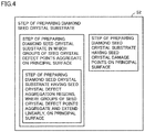
- the method for manufacturing a single-crystal diamond 20 includes a step S1 of forming a protective film 5 on at least a part of a surface of an auxiliary plate 4; a step S2 of preparing a diamond seed crystal substrate 10; a step S3 of disposing auxiliary plate 8 with a protective film, in which protective film 5 is formed on auxiliary plate 4, and diamond seed crystal substrate 10 in chamber 2; and s step S4 of growing single-crystal diamond 20 on a principal surface of diamond seed crystal substrate 10 by a chemical vapor deposition (hereinafter, also referred to as "CVD") method while introducing a carbon-containing gas into chamber 2.
- CVD chemical vapor deposition
- auxiliary plate 4 to be prepared in the method for manufacturing single-crystal diamond 20 according to this embodiment is not particularly limited, and molybdenum, copper, aluminum, niobium, tantalum, quartz, sapphire, alumina, magnesium oxide, strontium titanate, yttria-stabilized zirconia or the like, which is stable in an oxidizing/reducing atmosphere of hydrogen etc., and can be relatively inexpensively obtained as a plate having a large area, is suitably used.
- auxiliary plate 4 is formed of an oxide from the viewpoint of transmitting microwaves and being stable under a reducing atmosphere.
- auxiliary plate 4 is preferably greater than or equal to 1 mm and less than or equal to 5 mm, more preferably greater than or equal to 1 mm and less than or equal to 3 mm from the viewpoint of ease of handling.
- auxiliary plate 8 with a protective film in which protective film 5 is formed on auxiliary plate 4 is prepared by forming protective film 5 on at least a part of a surface of auxiliary plate 4 in step S 1 of forming a protective film on at least a part of a surface of an auxiliary plate in the method for manufacturing single-crystal diamond 20 according to this embodiment.
- Protective film 5 has a function of suppressing ingress of elements, which form auxiliary plate 4, into the single-crystal diamond, a function of suppressing ingress of impurity elements in chamber 2 into the single-crystal diamond, and so on as described in step S3 of disposing auxiliary plate 8 with a protective film, in which protective film 5 is formed on auxiliary plate 4, and diamond seed crystal substrate 10 in the chamber as described later.
- Protective film 5 can be obtained by, for example, forming a thin film of aluminum, titanium, vanadium, chromium, nickel, zirconium, niobium, molybdenum, hafnium, tantalum, tungsten, iridium or the like on a surface of auxiliary plate 4 using a vacuum sputtering method, a vacuum vapor deposition method, an ion plating method, an ion beam vapor deposition method or the like.
- protective film 5 is formed on a principal surface and a lateral surface of auxiliary plate 4.
- the thickness of protective film 5 is preferably greater than or equal to 0.5 ⁇ m, more preferably greater than or equal to 5 ⁇ m.
- the upper limit of the thickness of protective film 5 is not particularly limited, but is preferably less than or equal to 1000 ⁇ m from the viewpoint of ease of formation.
- Protective film 5 is effective when formed on at least a part of a surface of auxiliary plate 4.
- the protective film ratio (%) defined by the percentage ratio of the area of protective film 5 to the area of an exposed surface of auxiliary plate 4 is preferably greater than or equal to 10%, more preferably greater than or equal to 30%, still more preferably greater than or equal to 50%, still more preferably greater than or equal to 75%, most preferably 100%.
- protective film 5 contains a metal element serving as a getter of elements other than carbon from the viewpoint of suppressing ingress of impurity elements in chamber 2 into the single-crystal diamond.
- the getter refers to one that adsorbs impurity elements in a chamber to suppress ingress of the impurity elements into a single-crystal diamond.
- suitable metal element serving as a getter include metal elements that form a compound with oxygen, specifically aluminum, titanium, chromium, nickel, zirconium, molybdenum, hafnium, tungsten, iridium and the like.
- Step S2 of preparing diamond seed crystal substrate
- step S2 of preparing diamond seed crystal substrate 10 in the method for manufacturing single-crystal diamond 20 according to this embodiment is not particularly limited, but is preferably step S2 of preparing diamond seed crystal substrate 10 having seed crystal damage points on a principal surface 10m from the viewpoint of obtaining single-crystal diamond excellent in chipping resistance.
- the density of seed crystal damage points is preferably greater than or equal to 3 mm -2 , more preferably greater than or equal to 5 mm -2 .
- step S2 is preferably step S2 of preparing CVD (chemical vapor deposition) diamond seed crystal substrate 10 in which groups of crystal defect points aggregate on principal surface 10m.
- step S2 is more preferably step S2 of preparing diamond seed crystal substrate 10 having a seed crystal defect linear aggregation region in which groups of seed crystal defect points 10dp aggregate and extend linearly on principal surface 10m. That is, the method for manufacturing single-crystal diamond 20 includes the steps of: preparing diamond seed crystal substrate 10 having a seed crystal defect linear aggregation region in which groups of seed crystal defect points 10dp aggregate and extend linearly on principal surface 10m ( Fig. 9(A) ); and growing single-crystal diamond 20 on principal surface 10m of diamond seed crystal substrate 10 by a CVD (chemical vapor deposition) method ( Fig. 9(B) ).
- CVD chemical vapor deposition
- the principal surface basically refers to a crystal growth surface.
- the principal surface refers to a polished surface on a side close to the crystal growth surface.
- groups of crystal defect points aggregate is as follows. That is, crystal defect points 20dp are grouped such that a plurality of crystal defect points branched from one origination point or aggregations of crystal defect points branched in the middle between the origination point and the crystal defect points are put into one group, and crystal defect points derived from a different origination point are put into another group.
- the smallest circle encompassing all crystal defect points in the same group is expressed as an area of a group, groups aggregate when an area of a group is in contact with or overlaps with an area of another group.
- single-crystal diamond 20 in which groups of crystal defect points aggregate is obtained by growing single-crystal diamond 20 by a CVD method on principal surface 10m of diamond seed crystal substrate 10 which has seed crystal damage points with a density of preferably greater than or equal to 3 mm -2 , more preferably greater than or equal to 5 mm -2 on principal surface 10m, or principal surface 10m of diamond seed crystal substrate 10 in which groups of seed crystal defect points 10dp aggregate on principal surface 10m.
- Single-crystal diamond 20 is suitably used for cutting tools, polishing tools, optical components, electronic components, semiconductor materials and the like because stress is relaxed by a large number of groups of crystal defect points to suppress occurrence of large chipping.
- single-crystal diamond 20 in which a plurality of crystal defect linear aggregation regions 20r, where groups of crystal defect points 20dp that are tip points at which crystal defect lines 20dq reach a crystal growth principal surface 20m aggregate and extend linearly in a direction at an angle less than or equal to 30° with respect to one arbitrarily specified direction, are present in parallel is obtained by growing single-crystal diamond 20 by a CVD method on principal surface 10m of diamond seed crystal substrate 10 which has seed crystal defect linear aggregation regions where groups of seed crystal defect points 10dp aggregate and extend linearly on principal surface 10m.
- single-crystal diamond 20 stress is relaxed by a large number of crystal defect lines 20dq to suppress occurrence of large chipping, and a direction in which chipping hardly occurs can be controlled by a plurality of crystal defect linear aggregation regions 20r which are present in parallel, and extend linearly in a direction at an angle less than or equal to 30° with respect to one arbitrarily specified direction (see Figs. 5 and 6 ). Therefore, single-crystal diamond 20 is suitably used for cutting tools, polishing tools, optical components, electronic components, semiconductor materials and the like.
- the step of preparing diamond seed crystal substrate 10 having seed crystal defect linear aggregation regions, where groups of seed crystal defect points 10dp aggregate and extend linearly, on principal surface 10m is not particularly limited, and may include, for example, a step of forming irregularities on principal surface 10m of diamond seed crystal substrate 10.
- the reason why irregularities are formed is that seed crystal defect point 10dp corresponding to the irregularities can be formed.
- the depth of the irregularities on principal surface 10m is preferably greater than or equal to 0.1 nm and less than or equal to 100 nm, more preferably greater than or equal to 1 nm and less than or equal to 70 nm.
- the irregularities on principal surface 10m may be random, but it is preferable that groups of irregularities aggregate to form linearly extending seed crystal defect linear aggregation regions.
- the irregularities on principal surface 10m can be formed by etching, polishing, photolithography, a laser or the like.
- two or more seed crystal defect linear aggregation regions are present per 1 mm in a direction perpendicular to a direction in which the seed crystal defect linear aggregation regions extend linearly, and the distance between the seed crystal defect linear aggregation regions is less than or equal to 500 ⁇ m in the direction in which the regions extend linearly.
- two or more seed crystal defect linear aggregation regions are present per 1 mm in a direction perpendicular to a direction in which the seed crystal defect linear aggregation regions extend linearly, and the distance between the seed crystal defect linear aggregation regions is less than or equal to 500 ⁇ m in the direction in which the regions extend linearly.
- single-crystal diamond 20 can be obtained in which stress is relaxed by a large number of crystal defect lines 20dq to suppress occurrence of large chipping, and a direction in which chipping hardly occurs can be controlled by a plurality of dense crystal defect linear aggregation regions 20r which are present in parallel, and extend linearly in a direction at an angle less than or equal to 30° with respect to one arbitrarily specified direction.
- the pitch between a plurality of seed crystal linear aggregation regions which are present in parallel is preferably less than or equal to 500 ⁇ m, and more preferably less than or equal to 250 ⁇ m.
- the method for manufacturing single-crystal diamond 20 it is preferable that five or more long seed crystal defect linear aggregation regions having a length greater than or equal to 300 ⁇ m are present per 1 cm 2 of the principal surface.
- occurrence of large chipping in single-crystal diamond 20 to be grown is suppressed, and the strength of single-crystal diamond 20 as a whole is increased because five or more long seed crystal defect linear aggregation regions having a length greater than or equal to 300 ⁇ m are present per 1 cm 2 of the principal surface. From such a viewpoint, it is more preferable that twenty or more longer seed crystal defect linear aggregation regions having a length greater than or equal to 500 ⁇ m are present per 1 cm 2 of the principal surface.
- the density of seed crystal defect points 10dp is preferably greater than 10 mm -2 .
- the density of seed crystal defect points 10dp is greater than 10 mm -2 , and thus a single-crystal diamond in which the density of crystal defect points 20dp that are tip points at which crystal defect lines 20dq reach crystal growth principal surface 20m is greater than 20 mm -2 can be obtained by a CVD (chemical vapor deposition) method. Therefore, single-crystal diamond 20 can be obtained in which stress is relaxed by dense crystal defect lines 20dq to suppress occurrence of large chipping.
- the density of seed crystal defect points 10dp is more preferably greater than 100 mm -2 , still more preferably greater than 1000 mm -2 , especially preferably greater than 1 ⁇ 10 4 mm -2 .
- the density of seed crystal defect points 10dp is greater than 100 mm -2
- a single-crystal diamond in which the density of crystal defect points 20dp that are tip points at which crystal defect lines 20dq reach crystal growth principal surface 20m is greater than 300 mm -2 can be obtained by a CVD method.
- a single-crystal diamond in which the density of crystal defect points 20dp that are tip points at which crystal defect lines 20dq reach crystal growth principal surface 20m is greater than 1500 mm -2 can be obtained by a CVD method.
- a single-crystal diamond in which the density of crystal defect points 20dp that are tip points at which crystal defect lines 20dq reach crystal growth principal surface 20m is greater than 3000 mm -2 can be obtained by a CVD method.
- seed crystal defect points 10dp and seed crystal defect linear aggregation regions are favorably shown in an X-ray topographic image measured in a transmission mode in a direction perpendicular to principal surface 10m of diamond seed crystal substrate 10 (i.e. X-ray topographic image of principal surface 10m of diamond seed crystal substrate 10).
- the density of seed crystal damage points 10di indicating points at which crystal damage is present is preferably greater than 3 mm -2 in a secondary electron image in an electron microscope after principal surface 10m of diamond seed crystal substrate 10 is hydrogen-terminated.
- the density of seed crystal damage points 10di that generate a large number of crystal defect lines 20dq particularly in single-crystal diamond 20 grown by a chemical vapor deposition method, among seed defect points is greater than 3 mm -2 , and thus single-crystal diamond 20 having dense crystal defect lines 20dq can be obtained by a CVD (chemical vapor deposition) method.
- the density of seed crystal damage points 10di indicating points at which crystal damage is present is preferably greater than 30 mm -2 in a secondary electron image in an electron microscope after principal surface 10m of diamond seed crystal substrate 10 is hydrogen-terminated.
- the method for subjecting principal surface 10m of diamond seed crystal substrate 10 to a hydrogen termination treatment is not particularly limited, but from the viewpoint of effectively performing the treatment, principal surface 10m of diamond seed crystal substrate 10 is irradiated with a hydrogen plasma generated by introducing a microwave at 2.400 GHz to 2.497 GHz or 902 MHz to 928 MHz or performing heating with a hot filament under a reduced-pressure atmosphere fed with hydrogen gas.
- the temperature of diamond seed crystal substrate 10 is preferably less than or equal to 800°C, more preferably less than or equal to 600°C from the viewpoint of preventing a change in shape of principal surface 10m of diamond seed crystal substrate 10.
- the temperature of diamond seed crystal substrate 10 is preferably greater than or equal to 400°C so that hydrogen termination proceeds.
- the hydrogen termination treatment time is preferably greater than or equal to 3 minutes from the viewpoint of reliably performing the hydrogen termination treatment, and preferably less than or equal to 15 minutes from the viewpoint of ensuring that the substrate is not etched.
- principal surface 10m of diamond seed crystal substrate 10 hydrogen-terminated has a negative electronegativity, and therefore carriers excited by primary electrons from an electron microscope can be easily detected as secondary electrons, so that a secondary electron image can be observed as a distribution of defects that trap carriers in the crystal.
- principal surface 10m has distinct defects such as cracks as shown in Fig. 12 but also when principal surface 10m has no distinct defects as shown in Fig. 13 , crystal damages including fine cracks, fine strains and the like in addition to the above-mentioned crystal defects, and the density thereof can be evaluated.
- the above-mentioned crystal damages are observed as dark spots for fine cracks, and as light-dark changes for fine strains.
- the accelerating voltage is preferably less than or equal to 15 kV.
- the size of the principal surface of diamond seed crystal substrate 10 is preferably greater than or equal to 3 mm in diameter, more preferably greater than or equal to 6 mm, still more preferably greater than or equal to 10 mm in diameter from the viewpoint of growing a single-crystal diamond having a large diameter.
- step S2 of preparing diamond seed crystal substrate 10 for obtaining single-crystal diamond 20 in which groups of crystal defect points 20dp aggregate on principal surface 20m is not particularly limited, and from the viewpoint of efficiently preparing diamond seed crystal substrate 10 for obtaining single-crystal diamond 20 in which groups of crystal defects 20dp aggregate on principal surface 20m, step S2 may include a sub-step of forming seed crystal defect points 10dp and/or seed crystal damage points 10di on principal surface 10m of diamond seed crystal substrate 10; a sub-step of examining the density of seed crystal defect points 10dp and/or seed crystal damage points 10di on principal surface 10m of diamond seed crystal substrate 10; and a sub-step of forming a conductive layer region 10c by injecting ions on the principal surface 10m side of diamond seed crystal substrate 10.
- step S2 of preparing diamond seed crystal substrate 10 for obtaining single-crystal diamond 20 in which groups of crystal defect points 20dp aggregate on principal surface 20m is not particularly limited, and from the viewpoint of efficiently preparing diamond seed crystal substrate 10 in which groups of seed crystal defects 10dp aggregate on principal surface 10m, step S2 may include a sub-step of forming seed crystal defect points 10dp and/or seed crystal damage points 10di so that groups of seed crystal defect points 10dp aggregate on principal surface 10m of diamond seed crystal substrate 10; a sub-step of examining the density of seed crystal defect points 10dp and/or seed crystal damage points 10di on principal surface 10m of diamond seed crystal substrate 10; and a sub-step of forming a conductive layer region 10c by injecting ions on the principal surface 10m side of diamond seed crystal substrate 10.
- step S2 of preparing diamond seed crystal substrate 10 having seed crystal defect linear aggregation regions, where groups of seed crystal defect points 10dp aggregate linearly and extend linearly, on principal surface 10m is not particularly limited, and from the viewpoint of efficiently preparing diamond seed crystal substrate 10 having seed crystal defect linear aggregation regions, where groups of seed crystal defect points 10dp aggregate and extend linearly, on principal surface 10m, step S2 may include a sub-step of forming seed crystal defect linear aggregation regions, where groups of seed crystal defect points 10dp aggregate and extend linearly, on principal surface 10m of diamond seed crystal substrate 10; a sub-step of examining the density of seed crystal defect points 10dp and seed crystal damage points 10di on principal surface 10m of diamond seed crystal substrate 10; and a sub-step of forming a conductive layer region 10c by injecting ions on the principal surface 10m side of diamond seed crystal substrate 10.
- a Ib type single-crystal diamond or IIa type single-crystal diamond grown by a high-temperature and high-pressure method, and a single-crystal diamond grown by the CVD (chemical vapor deposition) method with the Ib type single-crystal diamond or IIa type single-crystal diamond as a seed crystal substrate are prepared.
- seed crystal defect points 10dp include various kinds of defect points such as seed crystal point defect points, seed crystal dislocation points 10dd (tip points at which dislocations such as edge dislocations, helical dislocations, and complex dislocations obtained by combining any of a plurality of edge dislocations and a plurality of helical dislocations reach principal surface 10m), seed crystal chipping points 10dv, seed crystal crack points and seed crystal damage points 10di.
- the method for forming a seed crystal defect linear aggregation region is not particularly limited, and the seed crystal defect linear aggregation region may be formed by, for example, forming a linear mask using a photolithography method, and then a plasma-etching a portion where a mask is not formed.
- the seed crystal defect linear aggregation region may be formed by laser processing.
- the seed crystal defect linear aggregation region may be formed by mechanical polishing with a whetstone obtained by bonding diamond abrasive grains with a metal, or a whetstone obtained by dispersing diamond abrasive grains in cast iron.
- cracks as origination points for dislocations can be further accurately controlled by performing reactive ion etching (RIE), microwave plasma etching or ion milling after such mechanical polishing.
- RIE reactive ion etching
- sccm oxygen
- CF 4 carbon tetrafluoride
- the direction in which seed crystal defect linear aggregation regions extend linearly is preferably a direction at an angle less than or equal to 30°, more preferably a direction at an angle less than or equal to 15° with respect to the ⁇ 100> direction.
- the crack refers to a hole made to a depth greater than or equal to 1 ⁇ m, or a linear crack having a length of 1 ⁇ m to 10 ⁇ m.
- the latter refers to a very small cleavage which is particularly easily formed principally in the ⁇ 110> direction.
- the crack point refers to a tip point at which a crack reaches principal surface 10m.
- the crystal damage refers to a very small hole made to a depth of less than 1 ⁇ m, and a very small crack of less than 1 ⁇ m, a crystal strain, or the like.
- the crystal damage point refers to a tip point at which a crystal damage reaches principal surface 10m.
- the arithmetic average roughness Ra (arithmetic average roughness Ra defined in JIS B 0601: 2013) of principal surface 10m after processing of a seed crystal is preferably 0.1 nm to 30 nm.
- principal surface 10m has an off angle of greater than or equal to 2° and less than or equal to 15° with respect to the (001) plane.
- the off direction of principal surface 10m is preferably at an angle less than or equal to 15° with respect to the ⁇ 100> direction, or at an angle less than or equal to 15° with respect to the ⁇ 110> direction.
- the off direction is not particularly limited, and it is preferable to perform CVD growth at a higher pressure as compared to a case where the off angle is greater than or equal to 2° and less than or equal to 15° with respect to the (001) plane of principal surface 10m.
- seed crystal defect linear aggregation regions are formed on principal surface 10m of diamond seed crystal substrate 10 in such a manner that two or more seed crystal defect linear aggregation regions are present per 1 mm in a direction perpendicular to a direction in which the seed crystal defect linear aggregation regions extend, and the distance between the seed crystal defect linear aggregation regions is less than or equal to 500 ⁇ m in the direction in which the regions extend linearly.
- the density of seed crystal defect points 10dp is confirmed to be greater than 10 mm -2 by observing an image in an optical microscope and/or X-ray topography.
- the density of seed crystal damage points 10di is confirmed to be greater than 3 mm -2 by observing a secondary electron image of principal surface 10 m in an electron microscope.
- the density of seed crystal defect points 10dp is less than or equal to 10 mm -2 and/or the density of seed crystal damage points 10di is less than or equal to 3 mm -2 , it is preferable to repeat the sub-step of forming seed crystal defect linear aggregation regions while changing conditions.
- the density of seed crystal defect points 10dp is greater than 1 ⁇ 10 6 mm -2 and/or the density of seed crystal damage points 10di is greater than 5 ⁇ 10 5 mm -2 , it is preferable to reduce at least one of the density of seed crystal defect points and the density of seed crystal damage points by etching etc.
- diamond seed crystal substrate 10 is of n-type in which a large number of donor atoms such as nitrogen atoms and phosphorus atoms are present, the band may rise near a hydrogen-terminated surface, leading to hindrance of release of secondary electrons.
- the donor density of diamond seed crystal substrate 10 is preferably less than or equal to 30 ppm, more preferably less than or equal to 1 ppm, and it is preferable that as diamond seed crystal substrate 10, a IIa type single-crystal diamond or a single-crystal diamond grown by a CVD (chemical vapor deposition) method is used.
- the sub-step of forming conductive layer region 10c on the principal surface 10m side of the diamond seed crystal substrate 10 is performed by implanting ions to the principal surface 10m side of diamond seed crystal substrate 10.
- ions ions of carbon, hydrogen, lithium, boron, nitrogen, oxygen or phosphorus are preferably used.
- Step S3 of disposing auxiliary substrate with protective film and diamond seed crystal substrate in chamber Step S3 of disposing auxiliary substrate with protective film and diamond seed crystal substrate in chamber
- a device for manufacturing a single-crystal diamond e.g. a CVD device 1 (chemical vapor deposition device) has a substrate support member 3 provided in chamber 2.
- chamber 2 is formed of a quartz tube, and substrate support member 3 is formed of copper.
- a substrate holder 6 is disposed on the upper surface of substrate support member 3.
- Diamond seed crystal substrate 10 is disposed on the upper surface of substrate holder 6.
- diamond seed crystal substrate 10 is disposed so as to expose principal surface 10m thereof.
- auxiliary plate 8 with a protective film in which protective film 5 is formed on auxiliary plate 4 is disposed on the upper surface of substrate support member 3.
- Auxiliary plate 8 with a protective film is disposed so as to expose at least a part of protective film 5.
- substrate holder 6 and auxiliary plate 8 with a protective film are disposed so as to cover the entire upper surface of substrate support member 3.
- raw material carbon is precipitated as graphite or diamond-like carbon on the upper surface of substrate support member 3 in growth of single-crystal diamond 20 on diamond seed crystal substrate 10 when the upper surface of substrate support member 3 formed of copper is exposed.
- Precipitated carbon such as graphite precipitated on substrate support member 3 is easily suspended in an atmosphere, and the precipitated carbon is caught in a single-crystal diamond grown on diamond seed crystal substrate 10.
- auxiliary plate 4 is disposed on the upper surface of substrate support member 3.
- Raw material carbon is also precipitated as graphite or the like on auxiliary plate 4, but since a quartz plate as auxiliary plate 4 is capable of firmly holding the precipitated carbon, the precipitated carbon is hardly suspended in an atmosphere. Therefore, by disposing a quartz plate as auxiliary plate 4 on substrate supporting member 3, precipitated carbon can be inhibited from being caught in the single-crystal diamond grown on diamond seed crystal substrate 10.
- quartz plate when a quartz plate is disposed as auxiliary plate 4 on substrate support member 3, silicon contained in the quartz plate is mixed in the single-crystal diamond as an impurity element in growth of single-crystal diamond 20 on diamond seed crystal substrate 10.
- auxiliary plate 8 with a protective film in which protective film 5 is formed on at least a part of a surface of auxiliary plate 4 is used, so that precipitated carbon can be inhibited from being caught in single-crystal diamond 20, and ingress of silicon into single-crystal diamond 20 can be suppressed.
- step S4 of growing single-crystal diamond 20 in the method for manufacturing single-crystal diamond 20 according to this embodiment is carried out by growing single-crystal diamond 20 on principal surface 10m of diamond seed crystal substrate 10 by a CVD method while introducing a carbon-containing gas into chamber 2.
- a CVD method a microwave plasma CVD method, a DC plasma CVD method, a hot filament CVD method or the like is suitably used.
- the carbon-containing gas CH 4 , C 2 H 6 , C 2 H 4 , C 2 H 2 , CH 3 OH, C 2 H 5 OH, (CH 3 ) 2 CO or the like is suitably used.
- single-crystal growing gas other than a carbon-containing gas hydrogen, argon, oxygen, carbon monoxide, carbon dioxide or the like is suitably used.
- the gas to be introduced into chamber 2 contains carbon and oxygen.
- Oxygen in the gas has an action of preventing ingress of impurity elements such as nitrogen and silicon into single-crystal diamond 20 and preferentially etching graphite formed concurrently with single-crystal diamond 20. Therefore, the resulting single-crystal diamond has a high purity and high light transmittance, and is optically transparent.
- a single-crystal diamond with a high purity can be grown by introducing a gas containing oxygen in addition to carbon, and using auxiliary plate 8 with a protective film in which protective film 5 is formed on at least a part of a surface of auxiliary plate 4.
- oxygen-containing gas for example, CO 2 , O 2 , CO, CH 3 OH, C 2 H 5 OH, (CH 3 ) 2 CO, H 2 O or the like is suitably used.
- the volume ratio of, for example, CH 4 , O 2 and H 2 in a combination of gases containing carbon and oxygen, which are introduced into chamber 2, is preferably 1 : 0.01 : 3 to 1 : 0.8 : 100, more preferably 1 : 0.05 : 3 to 1 : 0.8 : 100.
- the oxygen-containing gas etches single-crystal diamond 20 grown on diamond seed crystal substrate 10, so that the growth rate of single-crystal diamond 20 is reduced.
- the thickness of single-crystal diamond 20 to be grown is not particularly limited, but is preferably greater than or equal to 300 ⁇ m, more preferably greater than or equal to 500 ⁇ m from the viewpoint of favorably forming a semiconductor material, an electronic component, a heat dissipation component, an optical component, an electronic component, a cutting tool, a polishing tool or the like. From the viewpoint of preventing breakage caused by stress in diamond seed crystal substrate 10, the thickness of single-crystal diamond 20 is preferably less than or equal to 1500 ⁇ m, more preferably less than or equal to 1000 ⁇ m.
- first single-crystal diamond layer 21 having a thickness of less than or equal to 500 ⁇ m diamond seed crystal substrate 10 is then removed as described later, and a second single-crystal diamond layer 22 is then grown as additional single-crystal diamond 20 on first single-crystal diamond layer 21.
- first single-crystal diamond layer 21 and second single-crystal diamond layer 22 may be successively grown as single-crystal diamond 20 on diamond seed crystal substrate 10.
- single-crystal diamond 20 having a large thickness e.g. a thickness greater than 1000 ⁇ m
- first single-crystal diamond layer 21 having a thickness of less than or equal to 500 ⁇ m is formed, diamond seed crystal substrate 10 is then removed, and second single-crystal diamond layer 22 is then added and grown from the viewpoint of preventing breakage of diamond seed crystal substrate 10 due to an increase in thickness of single-crystal diamond 20.
- the method for manufacturing single-crystal diamond 20 according to this embodiment may further include a step of removing diamond seed crystal substrate 10 from the viewpoint of efficiently obtaining single-crystal diamond 20.
- the step of removing diamond seed crystal substrate 10 includes removing diamond seed crystal substrate 10 by laser cutting from the viewpoint of efficiently removing diamond seed crystal substrate 10.
- electrochemical etching such as electrolytic etching
- conductive layer region 10c formed by injecting ions into diamond seed crystal substrate 10 is decomposed and removed to remove diamond seed crystal substrate 10.
- the method for manufacturing single-crystal diamond 20 according to this embodiment may further include a step of adding and growing single-crystal diamond 20 from the viewpoint of obtaining single-crystal diamond 20 which is further inhibited from having large chipping.
- the step of adding and growing single-crystal diamond 20 is carried out by growing second single-crystal diamond layer 22 by a CVD method on the principal surface of first single-crystal diamond layer 21 which is single-crystal diamond 20 having been grown already.
- first single-crystal diamond layer 21 crystal defect lines 21dq originating from defects at seed crystal defect points 10dp on principal surface 10m of diamond seed crystal substrate 10 extend in a crystal growth direction as shown in Fig. 9(C) .
- second single-crystal diamond layer 22 grown on first single-crystal diamond layer 21 by a CVD method tips at which crystal defect lines 22dq originating from defects at crystal defect lines 21dq extend in a crystal growth direction and reach crystal growth principal surface 20m of single-crystal diamond 20 are crystal defect points 20dp.
- a plurality of crystal defect lines 21dq originate from one seed crystal defect point 10dp of diamond seed crystal substrate 10 in first single-crystal diamond layer 21, and a plurality of crystal defect lines 22dq originate from one crystal defect line 21dq of diamond seed crystal substrate 10 in second single-crystal diamond layer 22. Therefore, as the number of single-crystal diamond layers 21 and 22 increases, the number of crystal defect points 20dp of single-crystal diamond 20 increase, so that occurrence of large chipping is further suppressed.
- single-crystal diamond 20 which includes a plurality of single-crystal diamond layers 21 and 22 and in which crystal defect lines 21dq and 22dq are newly generated or branched at interfaces 212i between single-crystal diamond layers 21 and 22, and crystal defect points 20dp on crystal growth principal surface 20m are denser than crystal defect points 20ndp on a principal surface 20n opposite to crystal growth principal surface 20m as shown in Fig. 9(D) .
- the step of adding and growing single-crystal diamond 20 can be carried out by growing an additional single-crystal diamond by a CVD (chemical vapor deposition) method on principal surface 20n opposite to crystal growth principal surface 20 m of single-crystal diamond 20 obtained as in Fig. 9(C) .
- CVD chemical vapor deposition
- single-crystal diamond 20 which includes a plurality of single-crystal diamond layers 20a and 20b and in which crystal defect lines 20adq and 20bdq are newly generated, eliminated, branched or merged at interfaces 20i between single-crystal diamond layers 20a and 20b, and crystal defect points 20adp on a crystal growth principal surface 20am and crystal defect points 20bdp on a crystal growth principal surface 20bm opposite to crystal growth principal surface 20am are denser than crystal defect points at interfaces 20i between single-crystal diamond layers 20a and 20b as shown in Fig. 10 .
- the step of adding and growing single-crystal diamond 20 can be carried out by growing an additional single-crystal diamond by a CVD method on principal surface 20n opposite to crystal growth principal surface 20m of single-crystal diamond 20 obtained as in Fig. 9(D) .
- single-crystal diamond 20 which includes a plurality of single-crystal diamond layers 21a, 21b, 22a and 22b and in which crystal defect lines 21adq, 21bdq, 22adq and 22bdq are newly generated, eliminated, branched or merged at interfaces 20i, 212ai and 212bi between single-crystal diamond layers 21a, 21b, 22a and 22b, and crystal defect points 20adp on crystal growth principal surface 20am and crystal defect points 20bdp on crystal growth principal surface 20bm opposite to crystal growth principal surface 20am are denser than crystal defect points at interfaces 20i, 212ai and 212bi between single-crystal diamond layers 21a, 21b, 22a and 22b as shown in Fig. 11 .
- a single-crystal diamond according to this embodiment will be described with reference to Figs. 1 to 13 .
- single-crystal diamond 20 of this embodiment contains nitrogen as an impurity element in an amount of less than 500 ppb. Since single-crystal diamond 20 of this example contains nitrogen atoms as impurity element atoms only in an amount of less than 500 ppb, single-crystal diamond 20 has a low concentration of nitrogen atoms as heterogeneous element atoms that disturb extension of chipping in application of strong stress to a specific portion, and therefore, large chipping over a long distance easily occurs, but since a large number of crystal defect lines 20dq, 21dq and 22dq themselves, and relaxation of stress by the crystal defect lines disturb extension of chipping, occurrence of large chipping is suppressed.
- single-crystal diamond 20 of this example since the content of nitrogen atoms in single-crystal diamond 20 of this example is less than 500 ppb, single-crystal diamond 20 has a high light transmittance even when the number of crystal defects increases.
- the single-crystal diamond of this example is suitably used for applications of semiconductor materials (diodes, transistors and the like), electronic components (resistive parts, capacitive parts and the like), heat dissipation materials (heat sinks), optical components (window materials, lenses and the like), ornament materials, cutting tools, polishing tools and the like.
- the content of nitrogen in single-crystal diamond 20 is less than 500 ppb, preferably less than 250 ppb, more preferably less than 75 ppb, still more preferably less than 35 ppb, especially preferably less than 15 ppb.
- the content of nitrogen in single-crystal diamond 20 is measured by a SIMS (secondary ion mass spectrometry) method.
- SIMS secondary ion mass spectrometry
- the content of nitrogen is less than or equal to about 10 ppb, i.e. a lower detection limit in the SIMS method, the content is difficult to measure, and is therefore measured by an EPR (electron spin paramagnetic resonance) method.
- EPR electron spin paramagnetic resonance
- the content of nitrogen in single-crystal diamond 20 is adjusted by a volume ratio of a combination of a carbon-containing gas and an oxygen-containing gas in gases to be introduced into a chamber, a protective film ratio (%) defined by a percentage ratio of the area of protective film 5 to the area of an exposed surface of auxiliary plate 4, or the like.
- the volume ratio of CH 4 : O 2 : H 2 in a combination of gases is preferably 1 : 0.01 : 20 to 1 : 0.4 : 100, more preferably 1 : 0.03 : 20 to 1 : 0.4 : 100, and the protective film ratio is preferably greater than or equal to 30%, more preferably greater than or equal to 50%, still more preferably greater than or equal to 80%, especially preferably greater than or equal to 90%, most preferably 100%.
- single-crystal diamond 20 of this embodiment contains silicon as an impurity element in an amount of less than 1000 ppb. Since single-crystal diamond 20 of this example contains silicon atoms as impurity element atoms only in an amount of less than 1000 ppb, single-crystal diamond 20 has a low concentration of silicon atoms as heterogeneous element atoms that disturb extension of chipping in application of strong stress to a specific portion, and therefore large chipping over a long distance easily occurs, but since a large number of crystal defect lines 20dq, 21dq and 22dq themselves, and relaxation of stress by the crystal defect lines disturb extension of chipping, occurrence of large chipping is suppressed.
- single-crystal diamond 20 of this example since the content of silicon atoms in single-crystal diamond 20 of this example is less than 1000 ppb, single-crystal diamond 20 has a high light transmittance even when the number of crystal defects increases.
- the single-crystal diamond of this example is suitably used for applications of semiconductor materials (diodes, transistors and the like), electronic components (resistive parts, capacitive parts and the like), heat dissipation materials (heat sinks), optical components (window materials, lenses and the like), ornament materials, cutting tools, polishing tools and the like.
- the content of silicon in single-crystal diamond 20 is less than 1000 ppb, preferably less than 200 ppb, more preferably less than 50 ppb, still more preferably less than 5 ppb, especially preferably less than 0.05 ppb, most preferably less than 0.005 ppb.
- the content of silicon in single-crystal diamond 20 is measured by a SIMS method. When the content of silicon is less than or equal to about 1 ppb, i.e. a lower detection limit in the SIMS method, the content is difficult to measure, and is therefore measured by a low-temperature PL (photoluminescence) spectroscopic method.
- low-temperature PL spectroscopy measurement a sample is entirely cooled by liquid nitrogen, and green (514 nm) laser excitation is performed. A peak at 572 nm resulting from diamond and a peak at 737 nm resulting from silicon are observed in low-temperature PL spectroscopic measurement, and from a correlation between the intensity ratio of these peaks (737 nm/572 nm) and the quantitative value in the SIMS method, a silicon content of less than or equal to 1 ppb is measured.
- the lower detection limit in the low-temperature PL spectroscopic method is 0.0001 ppb.
- the content of silicon in single-crystal diamond 20 is adjusted by a volume ratio of a combination of a carbon-containing gas and an oxygen-containing gas to gases to be introduced into a chamber, a protective film ratio (%) defined by a percentage ratio of the area of protective film 5 to the area of an exposed surface of auxiliary plate 4, or the like.
- the volume ratio of CH 4 : O 2 : H 2 in a combination of gases is preferably 1 : 0.01 : 20 to 1 : 0.8 : 100, more preferably 1 : 0.05 : 20 to 1 : 0.8 : 100, and the protective film ratio is preferably greater than or equal to 30%, more preferably greater than or equal to 50%, still more preferably greater than or equal to 80%, especially preferably greater than or equal to 90%, most preferably 100%.
- single-crystal diamond 20 contains impurity elements other than nitrogen and silicon in an amount of less than 500 ppb. Since single-crystal diamond 20 of this example contains impurity element atoms other than nitrogen atoms and silicon atoms only in an amount of less than 500 ppb, single-crystal diamond 20 has a low concentration of impurity element atoms other than nitrogen atoms and silicon atoms, which are heterogeneous element atoms that disturb extension of chipping in application of strong stress to a specific portion, and therefore large chipping over a long distance easily occurs, but since a large number of crystal defect lines 20dq, 21bdq and 22dq themselves, and relaxation of stress by the crystal defect lines disturb extension of chipping, occurrence of large chipping is suppressed.
- single-crystal diamond 20 of this example since the content of impurity atoms other than nitrogen atoms and silicon atoms in single-crystal diamond 20 of this example is less than 500 ppb, single-crystal diamond 20 has a high light transmittance even when the number of crystal defects increases.
- the single-crystal diamond of this example is suitably used for applications of semiconductor materials (diodes, transistors and the like), electronic components (resistive parts, capacitive parts and the like), heat dissipation materials (heat sinks), optical components (window materials, lenses and the like), ornament materials, cutting tools, polishing tools and the like.
- the content of impurity elements other than nitrogen and silicon in the single-crystal diamond is less than 500 ppb, preferably less than 200 ppb, more preferably less than 100 ppb, still more preferably less than 75 ppb.
- the content of impurity elements other than nitrogen and silicon in the single-crystal diamond is measured by a SIMS method. When the content of impurity elements other than nitrogen and silicon is less than or equal to about 0.5 ppb, i.e. a lower detection limit in the SIMS method, the content is difficult to measure.
- impurity elements (atoms) other than nitrogen (atoms) and silicon (atoms) are elements (atoms) contained in auxiliary plate 4 and protective film 5 of auxiliary plate 8 with a protective film which is used in the method for manufacturing single-crystal diamond 20 according to the embodiment, and specific examples thereof include oxygen, magnesium, aluminum, titanium, chromium, nickel, copper, strontium, yttrium, zirconium, molybdenum, hafnium, tungsten and iridium.
- the transmittance of light having a wavelength of 500 nm may be greater than or equal to 55% when the single-crystal diamond has a thickness of 500 ⁇ m.
- the light transmittance when the single-crystal diamond has a thickness of 500 ⁇ m is a light transmittance measured when the single-crystal diamond has a thickness of 500 ⁇ m, or a light transmittance determined by measuring a light transmittance when the thickness of the single-crystal diamond is not 500 ⁇ m, and converting the measured light transmittance to a value when the single-crystal diamond has a thickness of 500 ⁇ m.
- the surface scattering ratio is less than or equal to 2%.
- a conventional single-crystal diamond absorbs light having a wavelength of 500 nm due to a synergistic effect of crystal defects and impurity atoms, so that the transmittance of light having such a wavelength decreases.
- single-crystal diamond 20 of this embodiment has a high purity, occurrence of large chipping is suppressed while the transmittance of light having a wavelength of 500 nm is greater than or equal to 55% when the thickness is 500 ⁇ m.
- the light transmittance in single-crystal diamond 20 of this embodiment means a regular transmittance with conversion performed for correcting surface scattering.
- single-crystal diamond 20 of this embodiment it is preferable that groups of crystal defect points 20dp that are tip points at which crystal defect lines 20dq indicating lines having crystal defects 20d in an X-ray topographic image for crystal growth principal surface 20m reach crystal growth principal surface 20m aggregate.
- a plurality of crystal defect linear aggregation regions 20r where groups of crystal defect points 20dp that are tip points at which crystal defect lines 20dq indicating lines having crystal defects 20d in an X-ray topographic image for crystal growth principal surface 20m reach crystal growth principal surface 20m aggregate and extend linearly in a direction at an angle less than or equal to 30° with respect to one arbitrarily specified direction, are present in parallel.
- Fig. 5 schematically shows an X-ray topographic image taken in a transmission mode, where crystal defect points 20dp that are tip points at which crystal defect lines 20dq reach crystal growth principal surface 20m are shown as black circle points so that crystal defect points 20dp can be easily identified.
- An Ib type single-crystal diamond which is widely used for cutting tools and abrasion-proof tools and which is grown by a high-temperature and high-pressure method contains a nitrogen impurity in isolated substitution type, and nitrogen atoms of isolated substitution type serve as origination points of plastic deformation to prevent occurrence of large chipping.
- nitrogen atoms of isolated substitution type hardly exist, and nitrogen atoms exist in the form of agglomerations with voids or a plurality of nitrogen atoms, which rather cause occurrence of large chipping.
- the present inventors have found that when a large number of dispersed crystal defects 20d are positively introduced into the CVD single-crystal diamond in such a manner that a plurality of crystal defect linear aggregation regions 20r, where groups of crystal defect points 20dp aggregate and extend linearly in a direction at an angle less than or equal to 30° with respect to one arbitrarily specified direction, are arranged in parallel, stress is relaxed, and therefore fine abrasions are promoted, so that large chipping making the single-crystal diamond unusable as a cutting tool hardly occurs.
- the present inventors have found that in a Ib type single-crystal diamond grown by a high-temperature and high-pressure method, it is difficult to introduce dispersed dislocations as in a CVD single-crystal diamond, a large number of dislocations are diffused radially from seed crystals, so that there is no anisotropy, or low crystal defect bundles are easily formed, chipping resistance is not improved, and thus improvement of chipping resistance by introduction of dislocations is unique to a CVD single-crystal diamond.
- single-crystal diamond 20 a plurality of crystal defect linear aggregation regions 20r, where groups of crystal defect points 20dp that are tip points at which crystal defect lines 20dq reach the crystal growth principal surface 20m aggregate and extend linearly in a direction at an angle less than or equal to 30° with respect to one arbitrarily specified direction, are present in parallel, so that stress is relaxed by a large number of crystal defect lines 20dq to suppress occurrence of large chipping, and a direction in which chipping hardly occurs can be controlled by a plurality of crystal defect linear aggregation regions 20r which are present in parallel, and extend linearly in a direction at an angle less than or equal to 30° with respect to one arbitrarily specified direction. Therefore, the single-crystal diamond is suitably used for cutting tools, polishing tools, optical components, electronic components, semiconductor materials and the like.
- the one arbitrarily specified direction is an average direction in which groups of crystal defect lines aggregate and extend linearly
- the one arbitrarily specified direction may be, for example, the ⁇ 110> direction in which abrasion resistance is high in the case of a cutting tool, or the ⁇ 100> direction in which abrasion is easy when consideration is given to productivity in a polishing step, and the direction can be selected according to a use purpose and a use method. It has been found that the directions in which groups of crystal defect lines aggregate and extend linearly may be dispersed to some extent, but when ⁇ shown in Fig. 6 is less than or equal to 30°, chipping resistance is more effectively improved.
- crystal defect points 20dp and crystal defect lines 20dq are shown in an X-ray topographic image of crystal growth principal surface 20m. That is, crystal defect points 20dp and crystal defect lines 20dq have a higher X-ray reflection intensity as compared to other portions of the crystal (portions having a smaller number of defects, i.e. portions having higher crystallinity), and therefore the presence thereof is shown as a dark spot in the case of a positive image, and as a light spot in the case of a negative image in an X-ray topographic image.
- crystal defects 20d include various kinds of defects such as point defects, dislocations, chipping, cracks and crystal strains.
- dislocations include edge dislocations, helical dislocations, and complex dislocations obtained by combining any of a plurality of edge dislocations and a plurality of helical dislocations.
- Crystal defect lines 20dq including crystal defects 20d are newly generated, or the lines are stopped when reaching crystal growth principal surface 20m.
- the tip of the crystal defect line 20dq, which reaches the crystal growth principal surface 20m, is called crystal defect point 20dp.
- the density is defined by counting the number of crystal defect points 20dp per unit area.
- an average value for five positions in an arbitrary region with a limited area may be employed.
- the number of crystal defect points is counted with the area limited such that a region of 1 mm square is selected when the number of crystal defect points is greater than or equal to 10/mm 2 , a region of 500 ⁇ m square is selected when the number of crystal defect points is greater than or equal to 100/mm 2 , and a region of 100 ⁇ m square is selected when the number of crystal defect points is greater than or equal to 1 ⁇ 10 4 /mm 2 , and the counted number of crystal defect points is converted to a value in mm -2 .
- the region where crystal defect points is counted is necessarily a portion including a crystal defect line aggregation region. If which side of the part where the crystal defect line is stopped reaches the crystal growth principal surface is not known, the incidence angle and the diffraction surface in a transmission type X-ray topographic image are changed, or a photograph is also taken in reflection type X-ray topography to reveal crystal defect points.
- Crystal defect points 20dp that are tip points of crystal defect lines 20dq that are lines having crystal defects 20d aggregate linearly on crystal growth principal surface 20m to form crystal defect linear aggregation region 20r.
- crystal defect linear aggregation region 20r is favorably shown in an X-ray topographic image measured in a transmission mode in a direction parallel to a crystal growth direction of single-crystal diamond 20 (i.e. direction perpendicular to crystal growth principal surface 20m).
- the X-ray topographic image can also be measured in a reflection mode, but an X-ray topographic image measured in a reflection mode is an image of overlapping crystal defect lines 20dq, and therefore it is difficult to clarify the aggregated state of crystal defect points 20dp.
- birefringence Birefringence method
- measurement may be performed using a laboratory type X-ray diffractometer.
- (111) diffraction may be observed with a Mo ray source
- (113) diffraction may be observed with a Cu ray source
- a long measurement time is required for taking a photograph at a high resolution.
- a nuclear plate is stored, developed and fixed in a cooling environment at 10°C or lower for avoiding an increase in noise. After development, an image is captured with an optical microscope, and crystal defect points and crystal defect lines are quantified.
- the crystal growth direction of single-crystal diamond 20 corresponds to an average direction of directions of a plurality of crystal defect lines 20dq.
- crystal growth principal surface 20m of the single-crystal diamond refers to the outermost crystal growth principal surface, which is generally perpendicular to the crystal growth direction.
- one arbitrarily specified direction as a reference is preferably be the ⁇ 100> direction, and is preferably a direction at an angle less than or equal to 30°, more preferably a direction at an angle less than or equal to 15° with respect to the ⁇ 100> direction. Since the single-crystal diamond is easily cleaved in the ⁇ 111> direction, and therefore when the direction in which crystal defect linear aggregation region 20r extends linearly is a direction as described above, chipping in single-crystal diamond 20 can be further suppressed.
- the diamond seed crystal substrate 10 that is used in growth of single-crystal diamond 20 by a CVD method is often a Ib type single-crystal grown by a high-temperature and high-pressure method
- single-crystal diamond 20 with the principal surface being parallel to the ⁇ 100> direction is easily obtained, and thus it is easy to obtain a tool having a large blade width, an optical component having a large area, an electronic component having a large area, a semiconductor material having a large area or the like.
- the ⁇ 110> direction is a direction in which crystal defect linear aggregation region 20r extends linearly.
- two or more crystal defect linear aggregation regions 20r are present per 1 mm in a direction perpendicular to a direction in which the crystal defect linear aggregation regions extend linearly (average direction of a plurality of directions in which a plurality of crystal defect linear aggregation regions extend, respectively, i.e. one specified direction as described above), and the distance D between the crystal defect linear aggregation regions is less than or equal to 500 ⁇ m in the direction in which the regions extend linearly.
- two or more crystal defect linear aggregation regions 20r are present per 1 mm in a direction perpendicular to a direction in which the crystal defect linear aggregation regions extend linearly, and the distance between the crystal defect linear aggregation regions is less than or equal to 500 ⁇ m in the direction in which the regions extend linearly.
- stress is relaxed by a large number of crystal defect lines 20dq to suppress occurrence of large chipping, and a direction in which chipping hardly occurs can be controlled by a plurality of dense crystal defect linear aggregation regions 20r which are present in parallel, and extend linearly in a direction at an angle less than or equal to 30° with respect to one arbitrarily specified direction.
- crystal defect linear aggregation regions 20r are present per 1 mm in a direction perpendicular to a direction in which the crystal defect linear aggregation regions linearly extend, and/or distance D between the crystal defect linear aggregation regions is less than or equal to 100 ⁇ m in the direction in which the regions extend linearly.
- a pitch P between a plurality of crystal linear aggregation regions 20r is preferably less than or equal to 500 ⁇ m, and more preferably less than or equal to 250 ⁇ m.
- single-crystal diamond 20 of this embodiment it is preferable that five or more long crystal defect linear aggregation regions 20r having a length L greater than or equal to 300 ⁇ m as shown in Fig. 6 are present per 1 cm 2 of crystal growth principal surface 20m.
- occurrence of chipping in single-crystal diamond 20 is suppressed, and the strength of single-crystal diamond 20 as a whole is increased because five or more long crystal defect linear aggregation regions having a length greater than or equal to 300 ⁇ m are present per 1 cm 2 of crystal growth principal surface 20m.
- the density of crystal defect points 20dp is preferably greater than 20 mm -2 , more preferably greater than 300 mm -2 , still more preferably greater than 1000 mm -2 , especially preferably greater than 1 ⁇ 10 4 mm -2 .
- occurrence of large chipping is suppressed due to relaxation of stress by dense crystal defect lines 20dq corresponding to dense crystal defect points 20dp because the density of crystal defect points 20dp is greater than 20 mm -2 .
- the density of crystal defect points 20dp is greater than 1000 mm -2
- the single-crystal diamond is excellent in chipping resistance even to intermittent cutting with a wiper tip.
- the density of crystal defect points 20dp is preferably less than 1 ⁇ 10 6 mm -2 .
- the density of complex dislocation points that are tip points at which complex dislocations obtained by combining any of a plurality of edge dislocations and a plurality of helical dislocations reach crystal growth principal surface 20m, among crystal defect points 20dp is preferably greater than 20 mm -2 , more preferably greater than 30 mm -2 , still more preferably greater than 300 mm -2 , especially preferably greater than 3000 mm -2 .
- occurrence of large chipping is further suppressed because the density of complex dislocation points that are tip points at which complex dislocations reach crystal growth principal surface 20m is greater than 20 mm -2 , and the effect of relaxing stress by complex dislocations is high.
- the density of complex dislocation points is greater than 300 mm -2 , the single-crystal diamond is excellent in chipping resistance even to intermittent cutting with a wiper tip.
- the density of complex dislocation points is preferably less than 3 ⁇ 10 5 mm -2 .
- the complex dislocation can be observed by changing the X-ray diffraction direction (g vector) in X-ray topography.
- the dislocation in observation of the (001) plane as crystal growth principal plane 20m of the diamond single crystal in a transmission mode, the dislocation is an edge dislocation when the (001) plane can be observed with a g vector in the [440] direction, but cannot be observed with a g vector in, for example, the [4-40] direction that is orthogonal to the g vector, and the dislocation is a complex dislocation when the (001) plane can be observed with a plurality of mutually orthogonal g vectors in, for example, the [440] direction and the [4-40] direction.
- the dislocations can be observed with g vectors in the [044] direction, the [004] direction, the [111] direction, the [113] direction and the like in a reflection mode.
- the image is overlapped by crystal defect lines 20dq of dislocations etc., and therefore it is difficult to determine whether crystal defects form a structure in the present invention.
- single-crystal diamond 20 of this embodiment includes a plurality of single-crystal diamond layers 21 and 22. Since single-crystal diamond 20 includes a plurality of single-crystal diamond layers 21 and 22, formation of crystal defect lines 21dq and 22dq is accelerated, so that occurrence of large chipping is further suppressed.
- first single-crystal diamond layer 21 grown by a CVD method on principal surface 10m of diamond seed crystal substrate 10 having seed crystal defect linear aggregation regions, where groups of seed crystal defect points 10dp aggregate and extend linearly, on principal surface 10m, crystal defect lines 21dq originating from defects at seed crystal defect points 10dp on principal surface 10m extend in a crystal growth direction.
- second single-crystal diamond layer 22 grown on first single-crystal diamond layer 21 by a CVD method tips at which crystal defect lines 22dq originating from defects at crystal defect lines 21dq extend in a crystal growth direction and reach crystal growth principal surface 20m of single-crystal diamond 20 are crystal defect points 20dp.
- a plurality of crystal defect lines 21dq originate from one seed crystal defect point 10dp of diamond seed crystal substrate 10 in first single-crystal diamond layer 21, and a plurality of crystal defect lines 22dq originate from one crystal defect line 21dq of first single-crystal diamond layer 21 in second single-crystal diamond layer 22. Therefore, as the number of single-crystal diamond layers 21 and 22 increases, the number of crystal defect points 20dp of single-crystal diamond 20 increase.
- Fig. 9(C) shows single-crystal diamond 20 obtained by removing diamond seed crystal substrate 10 from single-crystal diamond 20 grown on principal surface 10m of diamond seed crystal substrate 10 as shown in Fig. 7 .
- Fig. 9(D) shows single-crystal diamond 20 which includes a plurality of single-crystal diamond layers 21 and 22 and which is obtained by removing diamond seed crystal substrate 10 from single-crystal diamond 20 including a plurality of single-crystal diamond layers 21 and 22 grown on principal surface 10m of diamond seed crystal substrate 10 as shown in Fig. 8 .
- single-crystal diamond 20 includes a plurality of single-crystal diamond layers 21 and 22, and crystal defect lines 21dq and 22dq are newly generated or branched at interfaces 212i between singly-crystal diamond layers 21 and 22, and crystal defect points 20dp on crystal growth principal surface 20m are denser than crystal defect points 20ndp on a principal surface 20n opposite to crystal growth principal surface 20m.
- crystal defect lines 21dp and 22dp are newly generated or branched at interfaces between single-crystal diamond layers 21 and 22, and thus the number of crystal defect points 20dp at crystal growth principal surface 20m increases each time the number of single-crystal diamond layers 21 and 22 increases, so that crystal defect points 20dp at crystal growth principal surface 20m are denser than crystal defect points 20ndp at principal surface 20n opposite to crystal growth principal surface 20m, leading to further improvement of chipping resistance.
- Newly generated crystal defect lines may be branched and extend as shown in Fig. 9(D) .
- Fig. 10 shows a single-crystal diamond obtained by growing an additional single-crystal diamond on principal surface 20n opposite to crystal growth principal surface 20m of single-crystal diamond 20 shown in Fig. 9(C) .
- Fig. 11 shows a single-crystal diamond obtained by growing an additional single-crystal diamond including a plurality of single-crystal diamond layers on principal surface 20n opposite to crystal growth principal surface 20m of single-crystal diamond 20 including a plurality of single-crystal diamond layers 21 and 22 as shown in Fig. 9(D) .
- single-crystal diamond 20 of this embodiment includes a plurality of single-crystal diamond layers 20a, 20b, 21a, 21b, 22a and 22b, and crystal defect lines 20adq, 20bdq, 21adq, 21bdq, 22adq and 22bdq are newly generated, eliminated, branched or merged at interfaces 20i, 212ai and 212bi between single-crystal diamond layers 20a, 20b, 21a, 21b, 22a and 22b, and crystal defect points 20adp on crystal growth principal surface 20am and crystal defect points 20bdp on crystal growth principal surface 20bm opposite to crystal growth principal surface 20am are denser than crystal defect points at interfaces 20i, 212ai and 212bi between single-crystal diamond layers 20a, 20b, 21a, 21b, 22a and 22b.
- crystal defect lines 20adq,20bdq, 21adq, 21bdq, 22adq and 22bdq are newly generated, eliminated, branched or merged at interfaces 20i, 212a1 and 212bi between single-crystal diamond layers 20a, 20b, 21a, 21b, 22a and 22b, and thus the number of crystal defect points 20apd at crystal growth principal surface 20am and the number of crystal defect points 20bdp at opposite crystal growth principal surface 20bm increase each time the number of single-crystal diamond layers 20a, 20b, 21a, 21b, 22a and 22b increases, so that crystal defect points 20adp at crystal growth principal surface 20am and crystal defect points 20bdp at opposite crystal growth principal surface 20bm are denser than crystal defect points at interfaces 20i, 212ai and 212bi between single-crystal diamond layers 20a, 20b, 21a, 21b, 22a and 22b.
- single-crystal diamond 20 shown in Figs. 10 and 11 is obtained by growing single-crystal diamond layers 20a and 20b from interface 20i between the layers to crystal growth principal surfaces 20am and 20bm. Therefore, crystal defect lines 20adq and 20bdq are newly generated or branched from interface 20i in directions of both crystal growth principal surfaces 20am and 20bm.
- crystal defect lines 20adq, 21adq and 22adq are eliminated or merged between one crystal growth surface principal surface 20am and interface 20i, and crystal defect lines 20bdq, 21bdq and 22bdq are newly generated or branched between interface 20i and other crystal growth principal surface 20bm.
- the cross-section of the single-crystal diamond is cut, and measurement is performed.
- the cutting direction is set to the ⁇ 100> direction, and the cross-section is set to the (010) plane, it is easy to make discrimination in measurement, but the cutting direction may be other direction with the cross-section set to, for example, the (110) plane.
- single-crystal diamond 20 shown in Figs. 9(C) and 9(D) the density of crystal defect points 20dp at crystal growth principal surface 20m increases, and chipping resistance on the crystal growth principal surface 20m side is improved, but chipping resistance on the principal surface 20n side opposite to crystal growth principal surface 20m is not improved.
- single-crystal diamond 20 shown in Figs. 10 and 11 the density of crystal defect points 20adp at crystal growth principal surface 20am and crystal defect points 20bdp at opposite crystal growth principal surface 20bm increases, and therefore chipping resistance on both principal surface sides is improved.
- a material in which both a cutting surface and a brazed surface are strong enough to inhibit chipping, slipping-out of brazing and the like can be obtained from a single-crystal diamond having a nonuniform distribution of crystal defect lines in the thickness direction as described above.
- a CVD device 1 of this embodiment is CVD device 1 to be used in the method for manufacturing single-crystal diamond 20 according to embodiment 1, the device including chamber 2, and auxiliary plate 8 with a protective film, which is disposed in chamber 2 and in which protective film 5 is formed on at least a part of a surface of auxiliary plate 4.
- CVD device 1 of this embodiment includes auxiliary plate 8 with a protective film, which is disposed in chamber 2, and thus CVD device 1 is capable of manufacturing single-crystal diamond 20 of embodiment 2.
- substrate support member 3 is provided in chamber 2.
- chamber 2 is formed of a quartz tube, and substrate support member 3 is formed of copper.
- a substrate holder 6 is disposed on the upper surface of substrate support member 3.
- Diamond seed crystal substrate 10 is disposed on the upper surface of substrate holder 6.
- Diamond seed crystal substrate 10 is disposed so as to expose a principal surface thereof.
- Auxiliary plate 8 with a protective film in which protective film 5 is formed on auxiliary plate 4 is disposed on the upper surface of substrate support member 3.
- Auxiliary plate 8 with a protective film is disposed so as to expose at least a part of protective film 5.
- substrate holder 6 and auxiliary plate 8 with a protective film are disposed so as to cover the entire upper surface of substrate support member 3.
- a diamond seed crystal substrate of 5 mm ⁇ 5 mm ⁇ 1 mm (thickness) grown by a high-temperature and high-pressure method was prepared as diamond seed crystal substrate 10.
- principal surface 10m had an off angle of 2° to 10° in the ⁇ 100> direction with respect to the (001) plane.
- polishing scratches extending linearly in the ⁇ 100> direction were formed as seed crystal defect linear aggregation regions on principal surface 10m of each diamond seed crystal substrate 10 under the condition of a rotation speed of 500 rpm to 3000 rpm, a load of 0.5 kgf to 5 kgf and a polishing time of 30 minutes to 60 minutes using a whetstone obtained by fixing diamond grains having an average grain size of 9 ⁇ m to 35 ⁇ m with a metal.
- principal surface 10m of diamond seed crystal substrate 10 was polished under the condition of a rotation speed of 50 rpm, a load of 0.1 kgf and a polishing time of 600 minutes using a whetstone obtained by fixing diamond grains having an average grain size of 5 ⁇ m with a metal, so that there were almost no polishing scratches extending linearly in the ⁇ 100> direction as seed crystal defect linear aggregation regions.
- principal surface 10m of diamond seed crystal substrate 10 was then subjected to dry etching with an oxygen (O 2 ) gas and a hydrogen tetrafluoride (CF 4 ) gas to adjust the density of seed crystal defect points 10dp and seed crystal damage points 10di.
- O 2 oxygen
- CF 4 hydrogen tetrafluoride
- Conductive layer region 10c was then formed by ion-implanting carbon in a dose amount of 1 ⁇ 10 15 number • cm -2 to 1 ⁇ 10 18 number • cm -2 with an energy of 300 keV to 3 MeV on the principal surface 10m side of diamond seed crystal substrate 10 in each of samples 1-1 to 1-6, on which seed crystal defect linear aggregation regions were formed.
- single-crystal diamond 20 was grown by a microwave plasma CVD method on principal surface 10m of each diamond seed crystal substrate 10 on which seed crystal defect linear aggregation regions were formed.
- a quartz plate was used as an auxiliary plate to be disposed in a chamber of the microwave plasma CVD device, and an auxiliary plate with a protective film was obtained in which a protective film was formed on a principal surface and lateral surfaces of the quartz plate by a vacuum sputtering method.
- the type of the protective film, the protective film ratio, and the distance between the auxiliary plate with the protective film and the substrate are shown in Table 1.
- diamond seed crystal substrate 10 was disposed in substrate holder 6 in chamber 2 of CVD device 1, and auxiliary plate 8 with the protective film was disposed on substrate support member 3.
- a single-crystal diamond was grown at a crystal growth pressure of 25 kPa and a crystal growth temperature (diamond seed crystal substrate temperature of 1000°C by a microwave plasma CVD method.
- the volume ratio blending ratios of the gases here are shown in Table 1.
- diamond seed crystal substrate 10 was removed from single-crystal diamond 20 in each of samples 1-1 to 1-6 by decomposing and removing conductive layer region 10c in diamond seed crystal substrate 10 by electrolytic etching.
- the X-ray diffraction surface was set to the (220) plane.
- the energy of the X-ray used was 14.5
- single-crystal diamond 20 was further added and grown for samples 1-2, 1-3 and 1-5.
- the crystal growth conditions in the addition and growth were the same as the conditions for the above-described initial crystal growth.
- Thus-obtained single-crystal diamond 20 in each of samples 1-2, 1-3 and 1-5 had three single-crystal diamond layers.
- the X-ray diffraction surface was set to the (220) plane.
- the energy of the X-ray used was 14.5
- the contents of nitrogen, silicon, and impurity elements other than nitrogen and silicon in single-crystal diamond 20 were measured by a SIMS method.
- the content was less than or equal to a lower detection limit in the SIMS method, the content of nitrogen was measured using an EPR method in combination, and the content of silicon was measured using a low-temperature PL spectroscopic method in combination.
- a 500 ⁇ m-thick sample was formed from the obtained single-crystal diamond, and the transmittance of light having a wavelength of greater than or equal to 410 nm and less than or equal to 750 nm was measured by scanning the sample with a spectrophotometer at a wavelength ranging from 410 nm to 750 nm.
- the light transmittance at a wavelength of 500 nm was determined.
- the light transmittance in the single-crystal diamond of this example means a regular transmittance with conversion performed for correcting surface scattering.
- the measured transmittance is a transmittance measured at an incidence angle of 0° (perpendicular incidence) with respect to a surface of the sample.
- the measured conversion reflectance is a reflectance obtained in the following manner: the reflectance of light incident at an incidence angle of 10° with respect to a surface of the sample is converted to a reflectance in perpendicular reflection with an incidence angle of 0° and a reflection angle of 0° using a measured reflectance measured at a reflection angle of -10°.
- This conversion conforms to a general optical theoretical formula.
- the measured reflectance is measured with non-polarized light, and is therefore almost equal to the measured conversion reflectance.
- T T 1 2 • exp(- ⁇ D)/(1 - R 1 2 • exp(- ⁇ D))
- ⁇ is an absorption coefficient (unit: cm -1 )
- D is a distance (unit: cm -1 ) between the parallel principal surfaces.
- Chipping resistance was evaluated from the obtained single-crystal diamond in the following manner: an optical window material was laser-cut into a shape having a diameter of 3 mm, an end surface treatment was then performed by polishing the peripheral edge on the front and the back, and the number of chips of greater than or equal to 1 ⁇ m, which were generated at this time (chipping number) was determined. A sample having a small chipping number has high chipping resistance.
- the light transmittance defined as described above was greater than or equal to 55%.
- the chipping number defined as described above was 0. That is, it was found that for samples 1-1 to 1-4 prepared using both the auxiliary plate with the protective film and the diamond seed crystal substrate having seed crystal defect linear aggregation regions, the light transmittance defined as described above was as high as greater than or equal to 55%, and the chipping resistance defined as described above was high with the chipping number being 0. It was considered that the single-crystal diamond obtained in this example had a very high purity, and was hardly chipped due to the effect of controlling crystal defects.
- a diamond seed crystal substrate of 5 mm ⁇ 5 mm ⁇ 1 mm in thickness grown by the high-temperature high-pressure method and the CVD method and having the principal surface 10m with an off angle of 2° to 10° in the ⁇ 100> direction from the (001) was prepared.
- seed crystal damage points were formed on principal surface 10m of each diamond seed crystal substrate 10 under the condition of a rotation speed of 500 rpm to 3000 rpm, a load of 0.2 kgf to 2 kgf and a polishing time of 100 minutes to 150 minutes using a whetstone obtained by fixing diamond grains having an average grain size of 9 ⁇ m to 35 ⁇ m with a metal.
- sample II-7 principal surface 10m of diamond seed crystal substrate 10 was polished under the condition of a rotation speed of 50 rpm, a load of 0.1 kgf and a polishing time of 600 minutes using a whetstone obtained by fixing diamond grains having an average grain size of 5 ⁇ m with a metal, so that there were almost no polishing scratches as seed crystal defect linear aggregation regions.
- Sample II-8 was not evaluated as a seed substrate to be epitaxially grown, but evaluated with the sample subjected to normal polishing for optical properties as a reference.
- principal surface 10m of diamond seed crystal substrate 10 was then subjected to dry etching with an oxygen (O 2 ) gas and a hydrogen tetrafluoride (CF 4 ) gas to adjust the density of seed crystal defect points 10dp and seed crystal damage points 10di.
- O 2 oxygen
- CF 4 hydrogen tetrafluoride
- HPHT means that the substrate is a single-crystal substrate prepared by a high-temperature and high-pressure method
- CVD means that the substrate is a single-crystal substrate prepared by a chemical vapor deposition method.
- Sample II-8 was not evaluated as one grown on a seed substrate, but evaluated with the seed crystal substrate itself considered as a single-crystal diamond.
- Conductive layer region 10c was then formed by ion-implanting carbon in a dose amount of 1 ⁇ 10 15 number • cm -2 to 1 ⁇ 10 18 number • cm -2 with an energy of 300 keV to 3 MeV on the principal surface 10m side of diamond seed crystal substrate 10 in each of samples II-1 to II-7.
- single-crystal diamond 20 was grown by a microwave plasma CVD method on principal surface 10m of diamond seed crystal substrate 10 in each of samples II-1 to II-7, on which seed crystal defect linear aggregation regions were formed.
- a quartz plate was used as an auxiliary plate to be disposed in a chamber of the microwave plasma CVD device, and an auxiliary plate with a protective film was obtained in which a protective film was formed on a principal surface and lateral surfaces of the quartz plate by a vacuum sputtering method.
- the type of the protective film, the protective film ratio, and the distance between the auxiliary plate with the protective film and the substrate are shown in Table 2.
- diamond seed crystal substrate 10 was disposed in substrate holder 6 in chamber 2 of CVD device 1, and auxiliary plate 8 with the protective film was disposed on substrate support member 3.
- a single-crystal diamond was grown at a crystal growth pressure of 25 kPa and a crystal growth temperature (diamond seed crystal substrate temperature of 1000°C by a microwave plasma CVD method.
- the volume ratio blending ratios of the gases here are shown in Table 2.
- diamond seed crystal substrate 10 was removed from single-crystal diamond 20 in each of samples II-1 to II-7 by decomposing and removing conductive layer region 10c in diamond seed crystal substrate 10 by electrolytic etching.
- the X-ray diffraction surface was set to the (220) plane.
- the energy of the X-ray used was 14.5
- single-crystal diamond 20 was further added and grown for samples II-3 and II-6.
- the crystal growth conditions in the addition and growth were the same as the conditions for the above-described initial crystal growth.
- Thus-obtained single-crystal diamond 20 in each of samples II-3 and II-6 had three single-crystal diamond layers.
- the X-ray diffraction surface was set to the (220) plane.
- the energy of the X-ray used was 14.5
- the transmittance of light at a wavelength of 500 nm was determined by the same method as in Example 1.
- the expression and the meaning of the light transmittance were also the same as in Example 1.
- the light transmittance was greater than or equal to 55%.
- the chipping number was 0. That is, it was found that for samples II-1 to II-6 prepared using both the auxiliary plate with the protective film and the diamond seed crystal substrate having seed crystal defect linear aggregation regions, the light transmittance was as high as greater than or equal to 55%, and the chipping resistance was high with the chipping number being 0. It was considered that the single-crystal diamond obtained in this example had a very high purity, and was hardly chipped due to the effect of controlling crystal defects.
- sample II-8 was a cautiously prepared single-crystal diamond having no defects, a high purity and an almost ideal transmittance of 71%, but sample II-8 was easily chipped.
Landscapes
- Chemical & Material Sciences (AREA)
- Organic Chemistry (AREA)
- Engineering & Computer Science (AREA)
- Materials Engineering (AREA)
- Metallurgy (AREA)
- Chemical Kinetics & Catalysis (AREA)
- General Chemical & Material Sciences (AREA)
- Crystallography & Structural Chemistry (AREA)
- Mechanical Engineering (AREA)
- Inorganic Chemistry (AREA)
- Life Sciences & Earth Sciences (AREA)
- General Life Sciences & Earth Sciences (AREA)
- Geology (AREA)
- Manufacturing & Machinery (AREA)
- Physics & Mathematics (AREA)
- Combustion & Propulsion (AREA)
- Plasma & Fusion (AREA)
- Crystals, And After-Treatments Of Crystals (AREA)
- Chemical Vapour Deposition (AREA)
Applications Claiming Priority (2)
| Application Number | Priority Date | Filing Date | Title |
|---|---|---|---|
| JP2016010560 | 2016-01-22 | ||
| PCT/JP2017/001578 WO2017126561A1 (fr) | 2016-01-22 | 2017-01-18 | Diamant monocristallin, procédé destiné à la fabrication d'un diamant monocristallin, et dispositif de dépôt chimique en phase vapeur associé |
Publications (3)
| Publication Number | Publication Date |
|---|---|
| EP3406768A1 true EP3406768A1 (fr) | 2018-11-28 |
| EP3406768A4 EP3406768A4 (fr) | 2019-08-28 |
| EP3406768B1 EP3406768B1 (fr) | 2023-09-20 |
Family
ID=59362223
Family Applications (1)
| Application Number | Title | Priority Date | Filing Date |
|---|---|---|---|
| EP17741438.0A Active EP3406768B1 (fr) | 2016-01-22 | 2017-01-18 | Diamant monocristallin, procédé destiné à la fabrication d'un diamant monocristallin, et dispositif de dépôt chimique en phase vapeur associé |
Country Status (7)
| Country | Link |
|---|---|
| US (1) | US10737943B2 (fr) |
| EP (1) | EP3406768B1 (fr) |
| JP (1) | JP6795521B2 (fr) |
| KR (1) | KR102653291B1 (fr) |
| CN (1) | CN108474136B (fr) |
| SG (1) | SG11201805526PA (fr) |
| WO (1) | WO2017126561A1 (fr) |
Families Citing this family (5)
| Publication number | Priority date | Publication date | Assignee | Title |
|---|---|---|---|---|
| CN110387534A (zh) * | 2019-09-05 | 2019-10-29 | 蓬莱市超硬复合材料有限公司 | 一种纳米金刚石涂层硬质合金材料的制备方法 |
| CN111099586B (zh) * | 2019-11-27 | 2022-05-31 | 中国科学院金属研究所 | 一种纳米金刚石中高亮度硅空位色心的制备方法 |
| KR20230093253A (ko) * | 2020-10-22 | 2023-06-27 | 스미또모 덴꼬오 하드메탈 가부시끼가이샤 | 다이아몬드 소결체, 및 다이아몬드 소결체를 구비하는 공구 |
| CN113373512B (zh) * | 2021-05-24 | 2022-02-11 | 北京科技大学 | 基于铱-石墨烯结构化缓冲层的单晶金刚石外延生长方法 |
| US12565712B2 (en) * | 2023-05-24 | 2026-03-03 | Corey Albert Morrow | Method of manufacture of a watch crystal |
Family Cites Families (14)
| Publication number | Priority date | Publication date | Assignee | Title |
|---|---|---|---|---|
| JP3041844B2 (ja) * | 1995-08-11 | 2000-05-15 | 住友電気工業株式会社 | 成膜又はエッチング装置 |
| DE19826681B4 (de) | 1998-06-16 | 2004-02-12 | Marquardt, Niels, Dr. | Verfahren zur Herstellung von neuartigen Getter-Werkstoffen in Form dünner metallischer und kohlenstoffhaltiger nanostrukturierter Schichten und Verwendung derselben zur Hochvakuumerzeugung und Gasspeicherung |
| EP1290251B8 (fr) | 2000-06-15 | 2006-02-01 | Element Six (PTY) Ltd | Couche de diamant monocristallin epaisse, procede de fabrication, et pierres precieuses produites a partir de cette couche |
| WO2006048957A1 (fr) * | 2004-11-05 | 2006-05-11 | Sumitomo Electric Industries, Ltd. | Diamant monocristallin |
| JP5594613B2 (ja) * | 2005-04-15 | 2014-09-24 | 住友電気工業株式会社 | 単結晶ダイヤモンドおよびその製造方法 |
| KR20080044206A (ko) * | 2005-05-25 | 2008-05-20 | 카네기 인스티튜션 오브 워싱턴 | 신속한 성장 속도의 무색 단결정 cvd 다이아몬드 |
| US9133566B2 (en) * | 2005-12-09 | 2015-09-15 | Element Six Technologies Limited | High crystalline quality synthetic diamond |
| JP2009132948A (ja) * | 2007-11-28 | 2009-06-18 | Toyota Motor Corp | プラズマcvd装置 |
| EP2360289A1 (fr) * | 2010-02-23 | 2011-08-24 | Saint-Gobain Glass France | Dispositif et procédé de dépot d'une couche composée d'au moins deux composants sur un substrat |
| GB201021985D0 (en) | 2010-12-24 | 2011-02-02 | Element Six Ltd | Dislocation engineering in single crystal synthetic diamond material |
| GB201107552D0 (en) | 2011-05-06 | 2011-06-22 | Element Six Ltd | Diamond sensors, detectors, and quantum devices |
| GB201320304D0 (en) * | 2013-11-18 | 2014-01-01 | Element Six Ltd | Methods of fabricating synthetic diamond materials using microwave plasma actived chemical vapour deposition techniques and products obtained using said |
| KR102392424B1 (ko) * | 2014-07-22 | 2022-05-02 | 스미토모덴키고교가부시키가이샤 | 단결정 다이아몬드 및 그 제조 방법, 단결정 다이아몬드를 포함하는 공구, 및 단결정 다이아몬드를 포함하는 부품 |
| JP6594889B2 (ja) * | 2014-10-29 | 2019-10-23 | 住友電気工業株式会社 | 単結晶ダイヤモンド材料、ならびにそれを含む工具、放射温度モニター、および赤外光学部品 |
-
2017
- 2017-01-18 WO PCT/JP2017/001578 patent/WO2017126561A1/fr not_active Ceased
- 2017-01-18 JP JP2017562857A patent/JP6795521B2/ja active Active
- 2017-01-18 EP EP17741438.0A patent/EP3406768B1/fr active Active
- 2017-01-18 KR KR1020187020348A patent/KR102653291B1/ko active Active
- 2017-01-18 CN CN201780007532.XA patent/CN108474136B/zh active Active
- 2017-01-18 US US16/071,564 patent/US10737943B2/en active Active
- 2017-01-18 SG SG11201805526PA patent/SG11201805526PA/en unknown
Also Published As
| Publication number | Publication date |
|---|---|
| US10737943B2 (en) | 2020-08-11 |
| KR20180104617A (ko) | 2018-09-21 |
| US20190031515A1 (en) | 2019-01-31 |
| JPWO2017126561A1 (ja) | 2018-11-15 |
| WO2017126561A1 (fr) | 2017-07-27 |
| CN108474136A (zh) | 2018-08-31 |
| EP3406768A4 (fr) | 2019-08-28 |
| JP6795521B2 (ja) | 2020-12-02 |
| CN108474136B (zh) | 2021-05-28 |
| KR102653291B1 (ko) | 2024-03-29 |
| EP3406768B1 (fr) | 2023-09-20 |
| SG11201805526PA (en) | 2018-08-30 |
Similar Documents
| Publication | Publication Date | Title |
|---|---|---|
| EP3406768B1 (fr) | Diamant monocristallin, procédé destiné à la fabrication d'un diamant monocristallin, et dispositif de dépôt chimique en phase vapeur associé | |
| JP6708972B2 (ja) | 単結晶ダイヤモンドおよびその製造方法、単結晶ダイヤモンドを含む工具、ならびに単結晶ダイヤモンドを含む部品 | |
| JP7400879B2 (ja) | 炭化珪素基板および炭化珪素エピタキシャル基板 | |
| CN106661759B (zh) | 金刚石复合体、衬底、金刚石、包括金刚石的工具、以及制造金刚石的方法 | |
| US7771693B2 (en) | Diamond single crystal substrate manufacturing method | |
| KR102407952B1 (ko) | 단결정 다이아몬드, 단결정 다이아몬드의 제조 방법 및 단결정 다이아몬드를 이용한 공구 | |
| EP3828318A1 (fr) | Tranche de sic et procédé de fabrication de tranche de sic | |
| EP3822396A2 (fr) | Substrat de diamant et son procédé de fabrication | |
| WO2019019859A1 (fr) | Tranche de phosphure d'indium ayant des creux sur le coté arrière, procédé et solution de gravure pour sa fabrication | |
| WO2016068244A1 (fr) | Matériau en diamant monocristallin et outil mettant en oeuvre celui-ci, appareil de mesure de la température de rayonnement et pièce optique à rayonnement infrarouge | |
| EP1712661A1 (fr) | Diamant monocristal et son procédé de fabrication | |
| EP1832672B1 (fr) | Diamant monocristallin | |
| CN104508191A (zh) | 单晶金刚石和金刚石工具 | |
| US20240387640A1 (en) | SiC CRYSTAL SUBSTRATE, METHOD OF MANUFACTURING SiC CRYSTAL SUBSTRATE, SiC EPITAXIAL SUBSTRATE, AND METHOD OF MANUFACTURING SiC EPITAXIAL SUBSTRATE |
Legal Events
| Date | Code | Title | Description |
|---|---|---|---|
| STAA | Information on the status of an ep patent application or granted ep patent |
Free format text: STATUS: THE INTERNATIONAL PUBLICATION HAS BEEN MADE |
|
| PUAI | Public reference made under article 153(3) epc to a published international application that has entered the european phase |
Free format text: ORIGINAL CODE: 0009012 |
|
| STAA | Information on the status of an ep patent application or granted ep patent |
Free format text: STATUS: REQUEST FOR EXAMINATION WAS MADE |
|
| 17P | Request for examination filed |
Effective date: 20180720 |
|
| AK | Designated contracting states |
Kind code of ref document: A1 Designated state(s): AL AT BE BG CH CY CZ DE DK EE ES FI FR GB GR HR HU IE IS IT LI LT LU LV MC MK MT NL NO PL PT RO RS SE SI SK SM TR |
|
| AX | Request for extension of the european patent |
Extension state: BA ME |
|
| DAV | Request for validation of the european patent (deleted) | ||
| DAX | Request for extension of the european patent (deleted) | ||
| A4 | Supplementary search report drawn up and despatched |
Effective date: 20190725 |
|
| RIC1 | Information provided on ipc code assigned before grant |
Ipc: C30B 25/18 20060101ALI20190719BHEP Ipc: C30B 29/04 20060101AFI20190719BHEP Ipc: C30B 25/12 20060101ALI20190719BHEP Ipc: H01L 21/205 20060101ALI20190719BHEP Ipc: C23C 16/27 20060101ALI20190719BHEP Ipc: C30B 25/08 20060101ALI20190719BHEP Ipc: C23C 16/458 20060101ALI20190719BHEP Ipc: C23C 16/01 20060101ALI20190719BHEP Ipc: C23C 16/02 20060101ALI20190719BHEP Ipc: A44C 27/00 20060101ALI20190719BHEP Ipc: C01B 32/26 20170101ALI20190719BHEP Ipc: C30B 25/20 20060101ALI20190719BHEP |
|
| STAA | Information on the status of an ep patent application or granted ep patent |
Free format text: STATUS: EXAMINATION IS IN PROGRESS |
|
| 17Q | First examination report despatched |
Effective date: 20210928 |
|
| GRAP | Despatch of communication of intention to grant a patent |
Free format text: ORIGINAL CODE: EPIDOSNIGR1 |
|
| STAA | Information on the status of an ep patent application or granted ep patent |
Free format text: STATUS: GRANT OF PATENT IS INTENDED |
|
| RIC1 | Information provided on ipc code assigned before grant |
Ipc: H01L 21/02 20060101ALI20230329BHEP Ipc: C23C 16/458 20060101ALI20230329BHEP Ipc: C30B 25/18 20060101ALI20230329BHEP Ipc: C30B 25/12 20060101ALI20230329BHEP Ipc: C23C 16/02 20060101ALI20230329BHEP Ipc: H01L 21/205 20060101ALI20230329BHEP Ipc: C30B 25/20 20060101ALI20230329BHEP Ipc: C30B 25/08 20060101ALI20230329BHEP Ipc: C23C 16/27 20060101ALI20230329BHEP Ipc: C23C 16/01 20060101ALI20230329BHEP Ipc: C01B 32/26 20170101ALI20230329BHEP Ipc: A44C 27/00 20060101ALI20230329BHEP Ipc: C30B 29/04 20060101AFI20230329BHEP |
|
| INTG | Intention to grant announced |
Effective date: 20230425 |
|
| GRAS | Grant fee paid |
Free format text: ORIGINAL CODE: EPIDOSNIGR3 |
|
| GRAA | (expected) grant |
Free format text: ORIGINAL CODE: 0009210 |
|
| STAA | Information on the status of an ep patent application or granted ep patent |
Free format text: STATUS: THE PATENT HAS BEEN GRANTED |
|
| P01 | Opt-out of the competence of the unified patent court (upc) registered |
Effective date: 20230721 |
|
| AK | Designated contracting states |
Kind code of ref document: B1 Designated state(s): AL AT BE BG CH CY CZ DE DK EE ES FI FR GB GR HR HU IE IS IT LI LT LU LV MC MK MT NL NO PL PT RO RS SE SI SK SM TR |
|
| REG | Reference to a national code |
Ref country code: GB Ref legal event code: FG4D |
|
| REG | Reference to a national code |
Ref country code: CH Ref legal event code: EP |
|
| REG | Reference to a national code |
Ref country code: DE Ref legal event code: R096 Ref document number: 602017074413 Country of ref document: DE |
|
| REG | Reference to a national code |
Ref country code: IE Ref legal event code: FG4D |
|
| REG | Reference to a national code |
Ref country code: LT Ref legal event code: MG9D |
|
| PG25 | Lapsed in a contracting state [announced via postgrant information from national office to epo] |
Ref country code: GR Free format text: LAPSE BECAUSE OF FAILURE TO SUBMIT A TRANSLATION OF THE DESCRIPTION OR TO PAY THE FEE WITHIN THE PRESCRIBED TIME-LIMIT Effective date: 20231221 |
|
| REG | Reference to a national code |
Ref country code: NL Ref legal event code: MP Effective date: 20230920 |
|
| PG25 | Lapsed in a contracting state [announced via postgrant information from national office to epo] |
Ref country code: SE Free format text: LAPSE BECAUSE OF FAILURE TO SUBMIT A TRANSLATION OF THE DESCRIPTION OR TO PAY THE FEE WITHIN THE PRESCRIBED TIME-LIMIT Effective date: 20230920 Ref country code: RS Free format text: LAPSE BECAUSE OF FAILURE TO SUBMIT A TRANSLATION OF THE DESCRIPTION OR TO PAY THE FEE WITHIN THE PRESCRIBED TIME-LIMIT Effective date: 20230920 Ref country code: NO Free format text: LAPSE BECAUSE OF FAILURE TO SUBMIT A TRANSLATION OF THE DESCRIPTION OR TO PAY THE FEE WITHIN THE PRESCRIBED TIME-LIMIT Effective date: 20231220 Ref country code: LV Free format text: LAPSE BECAUSE OF FAILURE TO SUBMIT A TRANSLATION OF THE DESCRIPTION OR TO PAY THE FEE WITHIN THE PRESCRIBED TIME-LIMIT Effective date: 20230920 Ref country code: LT Free format text: LAPSE BECAUSE OF FAILURE TO SUBMIT A TRANSLATION OF THE DESCRIPTION OR TO PAY THE FEE WITHIN THE PRESCRIBED TIME-LIMIT Effective date: 20230920 Ref country code: HR Free format text: LAPSE BECAUSE OF FAILURE TO SUBMIT A TRANSLATION OF THE DESCRIPTION OR TO PAY THE FEE WITHIN THE PRESCRIBED TIME-LIMIT Effective date: 20230920 Ref country code: GR Free format text: LAPSE BECAUSE OF FAILURE TO SUBMIT A TRANSLATION OF THE DESCRIPTION OR TO PAY THE FEE WITHIN THE PRESCRIBED TIME-LIMIT Effective date: 20231221 Ref country code: FI Free format text: LAPSE BECAUSE OF FAILURE TO SUBMIT A TRANSLATION OF THE DESCRIPTION OR TO PAY THE FEE WITHIN THE PRESCRIBED TIME-LIMIT Effective date: 20230920 |
|
| REG | Reference to a national code |
Ref country code: AT Ref legal event code: MK05 Ref document number: 1613461 Country of ref document: AT Kind code of ref document: T Effective date: 20230920 |
|
| PG25 | Lapsed in a contracting state [announced via postgrant information from national office to epo] |
Ref country code: NL Free format text: LAPSE BECAUSE OF FAILURE TO SUBMIT A TRANSLATION OF THE DESCRIPTION OR TO PAY THE FEE WITHIN THE PRESCRIBED TIME-LIMIT Effective date: 20230920 |
|
| PG25 | Lapsed in a contracting state [announced via postgrant information from national office to epo] |
Ref country code: IS Free format text: LAPSE BECAUSE OF FAILURE TO SUBMIT A TRANSLATION OF THE DESCRIPTION OR TO PAY THE FEE WITHIN THE PRESCRIBED TIME-LIMIT Effective date: 20240120 |
|
| PG25 | Lapsed in a contracting state [announced via postgrant information from national office to epo] |
Ref country code: AT Free format text: LAPSE BECAUSE OF FAILURE TO SUBMIT A TRANSLATION OF THE DESCRIPTION OR TO PAY THE FEE WITHIN THE PRESCRIBED TIME-LIMIT Effective date: 20230920 |
|
| PG25 | Lapsed in a contracting state [announced via postgrant information from national office to epo] |
Ref country code: ES Free format text: LAPSE BECAUSE OF FAILURE TO SUBMIT A TRANSLATION OF THE DESCRIPTION OR TO PAY THE FEE WITHIN THE PRESCRIBED TIME-LIMIT Effective date: 20230920 |
|
| PG25 | Lapsed in a contracting state [announced via postgrant information from national office to epo] |
Ref country code: SM Free format text: LAPSE BECAUSE OF FAILURE TO SUBMIT A TRANSLATION OF THE DESCRIPTION OR TO PAY THE FEE WITHIN THE PRESCRIBED TIME-LIMIT Effective date: 20230920 Ref country code: RO Free format text: LAPSE BECAUSE OF FAILURE TO SUBMIT A TRANSLATION OF THE DESCRIPTION OR TO PAY THE FEE WITHIN THE PRESCRIBED TIME-LIMIT Effective date: 20230920 Ref country code: IS Free format text: LAPSE BECAUSE OF FAILURE TO SUBMIT A TRANSLATION OF THE DESCRIPTION OR TO PAY THE FEE WITHIN THE PRESCRIBED TIME-LIMIT Effective date: 20240120 Ref country code: ES Free format text: LAPSE BECAUSE OF FAILURE TO SUBMIT A TRANSLATION OF THE DESCRIPTION OR TO PAY THE FEE WITHIN THE PRESCRIBED TIME-LIMIT Effective date: 20230920 Ref country code: EE Free format text: LAPSE BECAUSE OF FAILURE TO SUBMIT A TRANSLATION OF THE DESCRIPTION OR TO PAY THE FEE WITHIN THE PRESCRIBED TIME-LIMIT Effective date: 20230920 Ref country code: CZ Free format text: LAPSE BECAUSE OF FAILURE TO SUBMIT A TRANSLATION OF THE DESCRIPTION OR TO PAY THE FEE WITHIN THE PRESCRIBED TIME-LIMIT Effective date: 20230920 Ref country code: AT Free format text: LAPSE BECAUSE OF FAILURE TO SUBMIT A TRANSLATION OF THE DESCRIPTION OR TO PAY THE FEE WITHIN THE PRESCRIBED TIME-LIMIT Effective date: 20230920 Ref country code: PT Free format text: LAPSE BECAUSE OF FAILURE TO SUBMIT A TRANSLATION OF THE DESCRIPTION OR TO PAY THE FEE WITHIN THE PRESCRIBED TIME-LIMIT Effective date: 20240122 Ref country code: SK Free format text: LAPSE BECAUSE OF FAILURE TO SUBMIT A TRANSLATION OF THE DESCRIPTION OR TO PAY THE FEE WITHIN THE PRESCRIBED TIME-LIMIT Effective date: 20230920 |
|
| PG25 | Lapsed in a contracting state [announced via postgrant information from national office to epo] |
Ref country code: PL Free format text: LAPSE BECAUSE OF FAILURE TO SUBMIT A TRANSLATION OF THE DESCRIPTION OR TO PAY THE FEE WITHIN THE PRESCRIBED TIME-LIMIT Effective date: 20230920 Ref country code: IT Free format text: LAPSE BECAUSE OF FAILURE TO SUBMIT A TRANSLATION OF THE DESCRIPTION OR TO PAY THE FEE WITHIN THE PRESCRIBED TIME-LIMIT Effective date: 20230920 |
|
| REG | Reference to a national code |
Ref country code: DE Ref legal event code: R097 Ref document number: 602017074413 Country of ref document: DE |
|
| PG25 | Lapsed in a contracting state [announced via postgrant information from national office to epo] |
Ref country code: DK Free format text: LAPSE BECAUSE OF FAILURE TO SUBMIT A TRANSLATION OF THE DESCRIPTION OR TO PAY THE FEE WITHIN THE PRESCRIBED TIME-LIMIT Effective date: 20230920 |
|
| PLBE | No opposition filed within time limit |
Free format text: ORIGINAL CODE: 0009261 |
|
| STAA | Information on the status of an ep patent application or granted ep patent |
Free format text: STATUS: NO OPPOSITION FILED WITHIN TIME LIMIT |
|
| PG25 | Lapsed in a contracting state [announced via postgrant information from national office to epo] |
Ref country code: DK Free format text: LAPSE BECAUSE OF FAILURE TO SUBMIT A TRANSLATION OF THE DESCRIPTION OR TO PAY THE FEE WITHIN THE PRESCRIBED TIME-LIMIT Effective date: 20230920 |
|
| PG25 | Lapsed in a contracting state [announced via postgrant information from national office to epo] |
Ref country code: MC Free format text: LAPSE BECAUSE OF FAILURE TO SUBMIT A TRANSLATION OF THE DESCRIPTION OR TO PAY THE FEE WITHIN THE PRESCRIBED TIME-LIMIT Effective date: 20230920 |
|
| 26N | No opposition filed |
Effective date: 20240621 |
|
| PG25 | Lapsed in a contracting state [announced via postgrant information from national office to epo] |
Ref country code: MC Free format text: LAPSE BECAUSE OF FAILURE TO SUBMIT A TRANSLATION OF THE DESCRIPTION OR TO PAY THE FEE WITHIN THE PRESCRIBED TIME-LIMIT Effective date: 20230920 |
|
| REG | Reference to a national code |
Ref country code: CH Ref legal event code: PL |
|
| PG25 | Lapsed in a contracting state [announced via postgrant information from national office to epo] |
Ref country code: LU Free format text: LAPSE BECAUSE OF NON-PAYMENT OF DUE FEES Effective date: 20240118 |
|
| PG25 | Lapsed in a contracting state [announced via postgrant information from national office to epo] |
Ref country code: LU Free format text: LAPSE BECAUSE OF NON-PAYMENT OF DUE FEES Effective date: 20240118 |
|
| PG25 | Lapsed in a contracting state [announced via postgrant information from national office to epo] |
Ref country code: BE Free format text: LAPSE BECAUSE OF NON-PAYMENT OF DUE FEES Effective date: 20240131 |
|
| PG25 | Lapsed in a contracting state [announced via postgrant information from national office to epo] |
Ref country code: FR Free format text: LAPSE BECAUSE OF NON-PAYMENT OF DUE FEES Effective date: 20240131 |
|
| PG25 | Lapsed in a contracting state [announced via postgrant information from national office to epo] |
Ref country code: CH Free format text: LAPSE BECAUSE OF NON-PAYMENT OF DUE FEES Effective date: 20240131 |
|
| PG25 | Lapsed in a contracting state [announced via postgrant information from national office to epo] |
Ref country code: SI Free format text: LAPSE BECAUSE OF FAILURE TO SUBMIT A TRANSLATION OF THE DESCRIPTION OR TO PAY THE FEE WITHIN THE PRESCRIBED TIME-LIMIT Effective date: 20230920 |
|
| PG25 | Lapsed in a contracting state [announced via postgrant information from national office to epo] |
Ref country code: SI Free format text: LAPSE BECAUSE OF FAILURE TO SUBMIT A TRANSLATION OF THE DESCRIPTION OR TO PAY THE FEE WITHIN THE PRESCRIBED TIME-LIMIT Effective date: 20230920 Ref country code: FR Free format text: LAPSE BECAUSE OF NON-PAYMENT OF DUE FEES Effective date: 20240131 Ref country code: CH Free format text: LAPSE BECAUSE OF NON-PAYMENT OF DUE FEES Effective date: 20240131 Ref country code: BE Free format text: LAPSE BECAUSE OF NON-PAYMENT OF DUE FEES Effective date: 20240131 |
|
| REG | Reference to a national code |
Ref country code: BE Ref legal event code: MM Effective date: 20240131 |
|
| PG25 | Lapsed in a contracting state [announced via postgrant information from national office to epo] |
Ref country code: BG Free format text: LAPSE BECAUSE OF FAILURE TO SUBMIT A TRANSLATION OF THE DESCRIPTION OR TO PAY THE FEE WITHIN THE PRESCRIBED TIME-LIMIT Effective date: 20230920 |
|
| PG25 | Lapsed in a contracting state [announced via postgrant information from national office to epo] |
Ref country code: BG Free format text: LAPSE BECAUSE OF FAILURE TO SUBMIT A TRANSLATION OF THE DESCRIPTION OR TO PAY THE FEE WITHIN THE PRESCRIBED TIME-LIMIT Effective date: 20230920 |
|
| PG25 | Lapsed in a contracting state [announced via postgrant information from national office to epo] |
Ref country code: CY Free format text: LAPSE BECAUSE OF FAILURE TO SUBMIT A TRANSLATION OF THE DESCRIPTION OR TO PAY THE FEE WITHIN THE PRESCRIBED TIME-LIMIT; INVALID AB INITIO Effective date: 20170118 |
|
| PG25 | Lapsed in a contracting state [announced via postgrant information from national office to epo] |
Ref country code: HU Free format text: LAPSE BECAUSE OF FAILURE TO SUBMIT A TRANSLATION OF THE DESCRIPTION OR TO PAY THE FEE WITHIN THE PRESCRIBED TIME-LIMIT; INVALID AB INITIO Effective date: 20170118 |
|
| PG25 | Lapsed in a contracting state [announced via postgrant information from national office to epo] |
Ref country code: TR Free format text: LAPSE BECAUSE OF FAILURE TO SUBMIT A TRANSLATION OF THE DESCRIPTION OR TO PAY THE FEE WITHIN THE PRESCRIBED TIME-LIMIT Effective date: 20230920 |
|
| PGFP | Annual fee paid to national office [announced via postgrant information from national office to epo] |
Ref country code: GB Payment date: 20251127 Year of fee payment: 10 |
|
| PGFP | Annual fee paid to national office [announced via postgrant information from national office to epo] |
Ref country code: IE Payment date: 20251209 Year of fee payment: 10 |
|
| PGFP | Annual fee paid to national office [announced via postgrant information from national office to epo] |
Ref country code: DE Payment date: 20251203 Year of fee payment: 10 |