EP3406961A1 - Dispositif d'éclairage et procédé associé - Google Patents
Dispositif d'éclairage et procédé associé Download PDFInfo
- Publication number
- EP3406961A1 EP3406961A1 EP18159107.4A EP18159107A EP3406961A1 EP 3406961 A1 EP3406961 A1 EP 3406961A1 EP 18159107 A EP18159107 A EP 18159107A EP 3406961 A1 EP3406961 A1 EP 3406961A1
- Authority
- EP
- European Patent Office
- Prior art keywords
- light
- electrically
- emitting device
- substrate
- radiation sources
- Prior art date
- Legal status (The legal status is an assumption and is not a legal conclusion. Google has not performed a legal analysis and makes no representation as to the accuracy of the status listed.)
- Withdrawn
Links
Images

Classifications
-
- H—ELECTRICITY
- H10—SEMICONDUCTOR DEVICES; ELECTRIC SOLID-STATE DEVICES NOT OTHERWISE PROVIDED FOR
- H10W—GENERIC PACKAGES, INTERCONNECTIONS, CONNECTORS OR OTHER CONSTRUCTIONAL DETAILS OF DEVICES COVERED BY CLASS H10
- H10W90/00—Package configurations
-
- B—PERFORMING OPERATIONS; TRANSPORTING
- B32—LAYERED PRODUCTS
- B32B—LAYERED PRODUCTS, i.e. PRODUCTS BUILT-UP OF STRATA OF FLAT OR NON-FLAT, e.g. CELLULAR OR HONEYCOMB, FORM
- B32B17/00—Layered products essentially comprising sheet glass, or glass, slag, or like fibres
- B32B17/06—Layered products essentially comprising sheet glass, or glass, slag, or like fibres comprising glass as the main or only constituent of a layer, next to another layer of a specific material
- B32B17/10—Layered products essentially comprising sheet glass, or glass, slag, or like fibres comprising glass as the main or only constituent of a layer, next to another layer of a specific material of synthetic resin
- B32B17/10005—Layered products essentially comprising sheet glass, or glass, slag, or like fibres comprising glass as the main or only constituent of a layer, next to another layer of a specific material of synthetic resin laminated safety glass or glazing
- B32B17/10009—Layered products essentially comprising sheet glass, or glass, slag, or like fibres comprising glass as the main or only constituent of a layer, next to another layer of a specific material of synthetic resin laminated safety glass or glazing characterized by the number, the constitution or treatment of glass sheets
- B32B17/10036—Layered products essentially comprising sheet glass, or glass, slag, or like fibres comprising glass as the main or only constituent of a layer, next to another layer of a specific material of synthetic resin laminated safety glass or glazing characterized by the number, the constitution or treatment of glass sheets comprising two outer glass sheets
-
- B—PERFORMING OPERATIONS; TRANSPORTING
- B32—LAYERED PRODUCTS
- B32B—LAYERED PRODUCTS, i.e. PRODUCTS BUILT-UP OF STRATA OF FLAT OR NON-FLAT, e.g. CELLULAR OR HONEYCOMB, FORM
- B32B17/00—Layered products essentially comprising sheet glass, or glass, slag, or like fibres
- B32B17/06—Layered products essentially comprising sheet glass, or glass, slag, or like fibres comprising glass as the main or only constituent of a layer, next to another layer of a specific material
- B32B17/10—Layered products essentially comprising sheet glass, or glass, slag, or like fibres comprising glass as the main or only constituent of a layer, next to another layer of a specific material of synthetic resin
- B32B17/10005—Layered products essentially comprising sheet glass, or glass, slag, or like fibres comprising glass as the main or only constituent of a layer, next to another layer of a specific material of synthetic resin laminated safety glass or glazing
- B32B17/10165—Functional features of the laminated safety glass or glazing
- B32B17/10541—Functional features of the laminated safety glass or glazing comprising a light source or a light guide
-
- F—MECHANICAL ENGINEERING; LIGHTING; HEATING; WEAPONS; BLASTING
- F21—LIGHTING
- F21K—NON-ELECTRIC LIGHT SOURCES USING LUMINESCENCE; LIGHT SOURCES USING ELECTROCHEMILUMINESCENCE; LIGHT SOURCES USING CHARGES OF COMBUSTIBLE MATERIAL; LIGHT SOURCES USING SEMICONDUCTOR DEVICES AS LIGHT-GENERATING ELEMENTS; LIGHT SOURCES NOT OTHERWISE PROVIDED FOR
- F21K9/00—Light sources using semiconductor devices as light-generating elements, e.g. using light-emitting diodes [LED] or lasers
- F21K9/90—Methods of manufacture
-
- F—MECHANICAL ENGINEERING; LIGHTING; HEATING; WEAPONS; BLASTING
- F21—LIGHTING
- F21V—FUNCTIONAL FEATURES OR DETAILS OF LIGHTING DEVICES OR SYSTEMS THEREOF; STRUCTURAL COMBINATIONS OF LIGHTING DEVICES WITH OTHER ARTICLES, NOT OTHERWISE PROVIDED FOR
- F21V23/00—Arrangement of electric circuit elements in or on lighting devices
- F21V23/06—Arrangement of electric circuit elements in or on lighting devices the elements being coupling devices, e.g. connectors
-
- H—ELECTRICITY
- H10—SEMICONDUCTOR DEVICES; ELECTRIC SOLID-STATE DEVICES NOT OTHERWISE PROVIDED FOR
- H10H—INORGANIC LIGHT-EMITTING SEMICONDUCTOR DEVICES HAVING POTENTIAL BARRIERS
- H10H20/00—Individual inorganic light-emitting semiconductor devices having potential barriers, e.g. light-emitting diodes [LED]
- H10H20/80—Constructional details
- H10H20/85—Packages
- H10H20/8506—Containers
-
- H—ELECTRICITY
- H10—SEMICONDUCTOR DEVICES; ELECTRIC SOLID-STATE DEVICES NOT OTHERWISE PROVIDED FOR
- H10H—INORGANIC LIGHT-EMITTING SEMICONDUCTOR DEVICES HAVING POTENTIAL BARRIERS
- H10H20/00—Individual inorganic light-emitting semiconductor devices having potential barriers, e.g. light-emitting diodes [LED]
- H10H20/80—Constructional details
- H10H20/85—Packages
- H10H20/857—Interconnections, e.g. lead-frames, bond wires or solder balls
-
- F—MECHANICAL ENGINEERING; LIGHTING; HEATING; WEAPONS; BLASTING
- F21—LIGHTING
- F21V—FUNCTIONAL FEATURES OR DETAILS OF LIGHTING DEVICES OR SYSTEMS THEREOF; STRUCTURAL COMBINATIONS OF LIGHTING DEVICES WITH OTHER ARTICLES, NOT OTHERWISE PROVIDED FOR
- F21V19/00—Fastening of light sources or lamp holders
- F21V19/001—Fastening of light sources or lamp holders the light sources being semiconductors devices, e.g. LEDs
- F21V19/0015—Fastening arrangements intended to retain light sources
- F21V19/002—Fastening arrangements intended to retain light sources the fastening means engaging the encapsulation or the packaging of the semiconductor device
-
- F—MECHANICAL ENGINEERING; LIGHTING; HEATING; WEAPONS; BLASTING
- F21—LIGHTING
- F21V—FUNCTIONAL FEATURES OR DETAILS OF LIGHTING DEVICES OR SYSTEMS THEREOF; STRUCTURAL COMBINATIONS OF LIGHTING DEVICES WITH OTHER ARTICLES, NOT OTHERWISE PROVIDED FOR
- F21V23/00—Arrangement of electric circuit elements in or on lighting devices
- F21V23/001—Arrangement of electric circuit elements in or on lighting devices the elements being electrical wires or cables
-
- F—MECHANICAL ENGINEERING; LIGHTING; HEATING; WEAPONS; BLASTING
- F21—LIGHTING
- F21Y—INDEXING SCHEME ASSOCIATED WITH SUBCLASSES F21K, F21L, F21S and F21V, RELATING TO THE FORM OR THE KIND OF THE LIGHT SOURCES OR OF THE COLOUR OF THE LIGHT EMITTED
- F21Y2105/00—Planar light sources
- F21Y2105/10—Planar light sources comprising a two-dimensional [2D] array of point-like light-generating elements
-
- F—MECHANICAL ENGINEERING; LIGHTING; HEATING; WEAPONS; BLASTING
- F21—LIGHTING
- F21Y—INDEXING SCHEME ASSOCIATED WITH SUBCLASSES F21K, F21L, F21S and F21V, RELATING TO THE FORM OR THE KIND OF THE LIGHT SOURCES OR OF THE COLOUR OF THE LIGHT EMITTED
- F21Y2105/00—Planar light sources
- F21Y2105/10—Planar light sources comprising a two-dimensional [2D] array of point-like light-generating elements
- F21Y2105/14—Planar light sources comprising a two-dimensional [2D] array of point-like light-generating elements characterised by the overall shape of the two-dimensional [2D] array
- F21Y2105/16—Planar light sources comprising a two-dimensional [2D] array of point-like light-generating elements characterised by the overall shape of the two-dimensional [2D] array square or rectangular, e.g. for light panels
-
- F—MECHANICAL ENGINEERING; LIGHTING; HEATING; WEAPONS; BLASTING
- F21—LIGHTING
- F21Y—INDEXING SCHEME ASSOCIATED WITH SUBCLASSES F21K, F21L, F21S and F21V, RELATING TO THE FORM OR THE KIND OF THE LIGHT SOURCES OR OF THE COLOUR OF THE LIGHT EMITTED
- F21Y2109/00—Light sources with light-generating elements disposed on transparent or translucent supports or substrates
-
- F—MECHANICAL ENGINEERING; LIGHTING; HEATING; WEAPONS; BLASTING
- F21—LIGHTING
- F21Y—INDEXING SCHEME ASSOCIATED WITH SUBCLASSES F21K, F21L, F21S and F21V, RELATING TO THE FORM OR THE KIND OF THE LIGHT SOURCES OR OF THE COLOUR OF THE LIGHT EMITTED
- F21Y2115/00—Light-generating elements of semiconductor light sources
- F21Y2115/10—Light-emitting diodes [LED]
-
- H—ELECTRICITY
- H10—SEMICONDUCTOR DEVICES; ELECTRIC SOLID-STATE DEVICES NOT OTHERWISE PROVIDED FOR
- H10H—INORGANIC LIGHT-EMITTING SEMICONDUCTOR DEVICES HAVING POTENTIAL BARRIERS
- H10H20/00—Individual inorganic light-emitting semiconductor devices having potential barriers, e.g. light-emitting diodes [LED]
- H10H20/01—Manufacture or treatment
- H10H20/036—Manufacture or treatment of packages
- H10H20/0364—Manufacture or treatment of packages of interconnections
Definitions
- the description relates to lighting devices.
- One or more embodiments may include electrically-powered light radiation sources, such as solid-state light radiation sources, e.g. LED sources.
- electrically-powered light radiation sources such as solid-state light radiation sources, e.g. LED sources.
- Illumination from glass has several potential applications, such as illumination from shower glazing, illumination from windows and door glazings, warning lights from vehicle windshields and so on.
- a conventional technology involves using an adhesive layer such as polyvinyl butyral (PVB), the bonding process taking place under heat and pressure.
- PVB polyvinyl butyral
- Assembling light radiation sources such as LEDs on glass may be expensive in view of the fairly sophisticated equipment and processes involved. Such an approach may also suffer from limitations e.g. in respect of the size of laminated glasses which can be produced.
- illumination from glass may involve placing light modules behind a glass panel.
- the light module and the glass panel may represent separate elements intended to be eventually assembled at the application site.
- Certain ones of these conventional techniques may permit to produce large-area light modules by connecting together various modules.
- An object of one or more embodiments is to contribute in providing improvements over conventional arrangements as discussed in the foregoing.
- One or more embodiments may relate to a corresponding method.
- One or more embodiments may be suitable for various glazing applications and meet user needs not met by conventional solutions.
- One or more embodiments make it possible to produce transparent flexible module designs e.g. in the form of continuous rolls.
- One or more embodiments may be cut to length and shape according to application and/or design requirements, with sections of modules adapted to be produced to suit a variety of e.g. glass sizes.
- such sections of modules can be laminated e.g. with glass, possibly before shipping for installation at an application site.
- a relatively large area of a light module can be laminated between e.g. glass panes and then cut to specific application lengths and/or sizes.
- One or more embodiments may be adapted for laminating between glass and/or plastics substrates such as glass and/or plastic panes.
- One or more embodiments may be adapted for laminating between glass and/or plastic panes which may be fully light-permeable (transparent) or exhibit varying degrees of transparency.
- references to "an embodiment” or “one embodiment” in the framework of the present description is intended to indicate that a particular configuration, structure, or characteristic described in relation to the embodiment is comprised in at least one embodiment.
- phrases such as “in an embodiment” or “in one embodiment” that may be present in one or more points of the present description do not necessarily refer to one and the same embodiment.
- particular conformations, structures, or characteristics may be combined in any adequate way in one or more embodiments.
- reference 100 designates as a whole a light-emitting device.
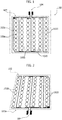
- the light-emitting device 100 includes a foil-like (e.g. plastic and/or light permeable) substrate 102 with electrically-powered light radiation sources 100a distributed thereon e.g. in a matrix arrangement.
- a foil-like (e.g. plastic and/or light permeable) substrate 102 with electrically-powered light radiation sources 100a distributed thereon e.g. in a matrix arrangement.
- the light radiation sources 100a may include electrically-powered light radiation sources such as solid-state light radiation sources. LED sources (e.g. as discussed in the following) may be exemplary of such light radiation sources.
- the device 100 as a "light-emitting device” takes into account the possibility of using such a device both as a stand-alone lighting device or as a component included in a more complex lighting device.
- One or more embodiments may provide a light-permeable (transparent) lighting module 100, suitable for lamination between glass and/or plastic panes as exemplified in Figure 4 to be discussed in the following.
- a light-emitting device as shown in Figure 1 may be included as a light-emitting layer 100 in an e.g. "stacked" structure of plural layers.
- a lighting device including a stacked arrangement of layers wherein a light-emitting device 100 as exemplified herein may be included as a light-emitting layer is disclosed in Italian Patent Application No. 102017000056197 filed in the name of the same Applicants.
- the flexible substrate 102 may include electrically-conductive lines (e.g. printed traces) 102a carrying electrical signals (power supply and, possibly, control) for the light radiation sources 100a to be distributed on the substrate 102.
- electrically-conductive lines e.g. printed traces
- electrical signals power supply and, possibly, control
- the electrically-conductive lines 102a may come down to a set of terminals 104 including e.g. power supply terminals (and, possibly, control terminals) for the device 100.
- the substrate 102 may include plastic material such as PEN (polyethylene naphthalate) foil and/or LEDs 100a of the Chip Scale Package (CSP) type.
- plastic material such as PEN (polyethylene naphthalate) foil and/or LEDs 100a of the Chip Scale Package (CSP) type.
- CSP Chip Scale Package
- the electrical traces 102a may be obtained by printing electrically-conductive ink (e.g. silver ink) onto the substrate 102.
- electrically-conductive ink e.g. silver ink
- traces 102a can be produced by resorting to other conventional techniques that are known per se.
- PEN substrate 102 facilitates achieving high clarity (e.g. in excess of 90%) of the substrate 102.
- CSP LEDs 100a makes it possible to take advantage of the 180° light directionality of CSP LEDs.
- a useful feature of such type of LEDs is the reduced thickness e.g. below 1 mm), that is such LEDs being (very) thin, and thus laminar by themselves. This facilitates lamination between glass and/or plastic panes, thus making it possible to produce very thin lighting devices for use e.g. as glazing.
- PEN for the substrate 102 and CSP LEDs for the light radiation sources 100a may facilitate obtaining layered structures (e.g. "sandwiches") of reduced thicknesses, with PEN exhibiting a good ability to withstand pressure and temperatures during lamination between e.g. glass and/or plastic panes.
- layered structures e.g. "sandwiches”
- PEN in combination with standard adhesive materials (e.g. polyvinyl butyral - PVB) in lamination processes with the ability of PEN to retain a high degree of clarity after the lamination process.
- standard adhesive materials e.g. polyvinyl butyral - PVB
- the light radiation sources 100a e.g. CSP LEDs
- the light radiation sources 100a can be assembled on the (e.g. PEN) substrate 102 by using a solder paste reflowing at low temperatures (e.g. by means of a low-temperature solder process), with the paste including e.g. metal spheres (balls) with an epoxy compound.
- Such a low-temperature assembly method may facilitate achieving solder joints having a higher reliability than joints obtained through the use of e.g. a conventional isotropic conductive paste.
- PEN offers higher process robustness than, say, polyethylene terephtalate (PET) and a lower cost than polyimide (PI)
- PET polyethylene terephtalate
- PI polyimide
- (ink) printing may represent a viable option for producing the electrically-conductive formations or lines 102a well suited for use with PEN as the substrate material (primarily due to printing preserving the substrate transparency)
- other types of arrangements may be adopted for producing the electrically-conductive lines 102a.
- Rolled annealed or electro-deposited electrically-conductive materials may represent other options for use in embodiments.
- exemplary devices 100 as exemplified herein may include a matrix-like arrangements of LEDs 100a including e.g. a 6x8 matrix arrangement of LEDs of 1.20x0.8mm each.
- the pattern of electrically-conductive lines (traces) 102a may be intended to facilitate good thermal dissipation properties.
- Figures 1 and 2 are exemplary of a possible layout of traces 102a including sections 1020 between the light sources 100a of an enlarged e.g. elliptical (or round) shape: such a shape may facilitate heat dissipation.
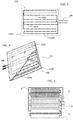
- Embodiments as exemplified in Figures 3 and 4 as well as in Figures 6 to 11 are exemplary of embodiments wherein a leaner (i.e. wire-like) design may be adopted for subsequent sections 1020 of the electrically-conductive traces 102a in order to increase the amount of the area of the transparent substrate 102 not covered by the (e.g. printed) traces 102a.
- a leaner i.e. wire-like
- electrically-conductive traces 102a may be provided by e.g. printing an electrically-conductive material (such as silver ink) thus facilitating achieving good thermal dissipation properties even in the presence of a thinner trace design.
- an electrically-conductive material such as silver ink
- an increase in the transparent area may be obtained by using light-permeable (e.g. transparent) materials; a light-permeable ink (such as ITO - Indium Tin Oxide) may be exemplary of such material).
- light-permeable e.g. transparent
- a light-permeable ink such as ITO - Indium Tin Oxide
- Figure 4 is exemplary of the possibility of producing a lighting device 10 by laminating a light-emitting device or layer 100 as discussed previously (e.g. with a trace pattern as exemplified in Figure 3 ) between two panes e.g. glass and/or plastic panes 110a, 110b.
- a sandwiched arrangement as exemplified in Figure 4 may include a layout of electrically-conductive lines (traces) 102a as exemplified in Figures 1 and 2 in the place of the layout exemplified in Figure 3 .
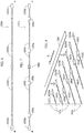
- Figure 5 is generally exemplary of a possible approach which may be adopted in providing a flexible printed circuit (FPC) structure as exemplified herein.
- FPC flexible printed circuit
- Figure 5 may regarded as including three sections, designated A, B and C, respectively, and corresponding to three separate strings of light radiation sources 100a.
- Each such string may include a set of sources (e.g. LEDs) connected in series.
- sources e.g. LEDs
- One or more embodiments may address issues related to shower/bathroom glazing applications and the associated safety requirements, compatible with a commercial design of a laminated film (light module) in glass.
- a laminated film approach provides a roll of film, which can handled relatively easily in existing glass lamination process, with the possibility of being "customized" to the required sizes of glass panels.
- a low-voltage (e.g., 12V DC) solution is desirable in order to meet with safety requirements for shower/bathroom glazing application and similar applications (e.g. glazed glass for outdoor applications, bus terminals, train terminals, etc .... ).
- One or more embodiments may provide, e.g., a LED layout complying with optical requirements and adopting a (big size) bus bar connection providing an adequate power supply from a low-voltage source even for lighting devices 10 of large dimensions.
- One or more embodiments as exemplified, e.g. in Figures 6 to 11 may also provide homogeneous surface lighting (non-appreciable "hot spots"), flexibility also at the lighting portions while being compatible with dimming of LED sources.
- a device 100 as exemplified herein can be made resizable (that is adapted to be cut from a roll at a desired length).
- the connectors e.g., 104 in Figure 4
- the connectors can be integrated at the end of the manufacturing process.
- One or more embodiments may facilitate achieving good robustness of the LEDs (100a in the figures) after lamination (this applying, i.a., to the LED temperature within the glass and to phosphor robustness).
- Figures 6 and 7 are exemplary of the electrically-conductive traces 102a which facilitate 12V DC operation. This in turn facilitates (electrical) safe shower/bathroom glazing application.
- the electrically-conductive traces 102a can be realized as single electrical units (SEU's), of a length of e.g. 95,5 mm, including four LEDs 100a and an intermediate resistor 100b for current balancing.
- SEU's single electrical units
- the electrically-conductive traces 102a providing a conductive pattern/circuitry as exemplified herein can be produced by (e.g. screen-) printing electrically-conductive ink (e.g. silver-based ink) on a transparent/semitransparent polymeric substrate 102 (comprising e.g. a PEN, PET foil) or by etched copper technology on a transparent/semitransparent substrate 102 or a mix of the two technologies.
- electrically-conductive ink e.g. silver-based ink
- a transparent/semitransparent polymeric substrate 102 comprising e.g. a PEN, PET foil
- etched copper technology e.g. a transparent/semitransparent substrate 102 or a mix of the two technologies.
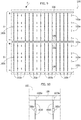
- the rectilinear SEUs (see again Figures 6 and 7 ) in the electrically-conductive traces 102a are arranged mutually parallel. This facilitates wrapping or winding the device 10 to a roll in a direction as exemplified by the arrow R in Figure 8 .
- high illuminance, low luminance, high uniformity (virtually no hot spots) and glare control are desirable features which are (quite) difficult to achieve in large size glazing application.
- the foregoing corresponds to a density of about 3200 LEDs/m 2 and a surface occupancy (circuitry area/apparent area) of about 23%.
- One or more embodiments may adopt a general layout as exemplified in Figure 9 , that is with the SEUs having at their ends terminal contact lands 1020a to which electrically-conductive strip-like bus-bars 106 can be coupled.
- This arrangement has the advantage of being simple and symmetrical.
- the limited electrical conductivity of standard conductive inks can be taken into account by using (e.g. for long-haul applications) a hybrid configuration, wherein:
- bus-bars may comprise, e.g. 1 oz, metal Cu tape with an adhesive side adapted to be applied on the printed ink circuitry. Soldering of bus-bars may be a further option, while possibly suffering from thermal issues.
- the high conductivity of standard copper possibly in combination with the adoption of bus-bars with a large cross-section (e.g. continuous bus-bar - 1 oz), facilitates connecting several meters of flex for a continuous roll, e.g. for carrying high currents with a limited voltage drop.
- a bus bar 106 comprising e copper tape with electrically-conductive adhesive on the bottom makes it possible to directly connect the 12V DC main line to the +/- pads 1020a.
- An arrangement as exemplified in Figure 9 has the advantage of being simple and symmetric, including two sub-arrays A and B (rows) connectable in parallel (see e.g. the + and - signs in Figure 9 ) to a mains 12V DC power supply.
- bus-bar connection layouts are of course possible, e.g., having less or more than four bus bars as exemplified herein (with possible limitations on the size of bus-bars 106 - that may become larger, thus decreasing the transparency of the light-emitting device - and on their electrical current load, that may increase).
- Figure 11 is exemplary of one or more embodiments where a light-emitting device 100 including the arrangement of parallel SEUs 102a and bus-bar 106 formed onto a substrate 102 is laminated between two panes e.g. glass and/or plastic panes 110a, 110b - as already discussed in connection with Figure 4 - with two light-permeable (adhesive or non-adhesive) lamination layers 112a (top) and 112b (bottom) set between the light-emitting device 100 and the panes 110a and 110b, respectively.
- two panes e.g. glass and/or plastic panes 110a, 110b - as already discussed in connection with Figure 4 - with two light-permeable (adhesive or non-adhesive) lamination layers 112a (top) and 112b (bottom) set between the light-emitting device 100 and the panes 110a and 110b, respectively.
- a light-emitting device (e.g. 100) according to one or more embodiments may include:
- the light-permeable substrate may include plastics material, optionally selected out of polyethylene naphtalate - PEN, polyethylene terephtalate - PET, and polyimide - PI.
- the light-permeable substrate may include polyethylene naphtalate - PEN.
- the electrically-powered light radiation sources may include solid-state light radiation sources such as LED sources.
- the electrically-powered light radiation sources may include LED sources of the Chip Scale Package - CSP type.
- One or more embodiments may include low-temperature solder paste coupling the light radiation sources to the substrate.
- the low-temperature solder paste includes metal spheres with an epoxy compound.
- the electrically-conductive formations may include printed formations on the laminar substrate.
- the electrically-conductive formations may include expanded portions (see e.g. 1020 in Figures 1 and 2 ) between the light radiation sources.
- the electrically-conductive formations may include wire-like electrically-conductive formations (see e.g. 1020 in Figure 3 ).
- a light-emitting device may be laminated with at least one light-permeable pane (e.g. 110a, 110b).
- a light-emitting device may be sandwiched between two light-permeable panes (e.g. 110a, 110b).
- the light-emitting device may be sandwiched between two light-permeable panes with light-permeable lamination layers (e.g. 112a, 112b) set between the light-emitting device and the light-permeable panes.
- light-permeable lamination layers e.g. 112a, 112b
- bus-bars are couplable (see e.g. the terminals 104) to a supply source, such as e.g. a low-voltage (e.g. 12V DC) supply source.
- a supply source such as e.g. a low-voltage (e.g. 12V DC) supply source.
- One or more embodiments may comprise a plurality (e.g. A, B) of said arrays of electrically-conductive formations jointly couplable to a supply source via respective electrically-conductive bus-bars.
- a method of providing light-emitting devices (100) may include:
- One or more embodiments may include coupling the light radiation sources to the substrate with a low-temperature solder process.
- One or more embodiments may include coupling the light radiation sources to the substrate with a low-temperature solder paste including metal spheres with an epoxy compound.
Landscapes
- Engineering & Computer Science (AREA)
- General Engineering & Computer Science (AREA)
- Manufacturing & Machinery (AREA)
- Physics & Mathematics (AREA)
- Microelectronics & Electronic Packaging (AREA)
- Optics & Photonics (AREA)
- Electroluminescent Light Sources (AREA)
Applications Claiming Priority (1)
| Application Number | Priority Date | Filing Date | Title |
|---|---|---|---|
| IT201700056220 | 2017-05-24 |
Publications (1)
| Publication Number | Publication Date |
|---|---|
| EP3406961A1 true EP3406961A1 (fr) | 2018-11-28 |
Family
ID=59859572
Family Applications (1)
| Application Number | Title | Priority Date | Filing Date |
|---|---|---|---|
| EP18159107.4A Withdrawn EP3406961A1 (fr) | 2017-05-24 | 2018-02-28 | Dispositif d'éclairage et procédé associé |
Country Status (2)
| Country | Link |
|---|---|
| US (1) | US20180342491A1 (fr) |
| EP (1) | EP3406961A1 (fr) |
Cited By (1)
| Publication number | Priority date | Publication date | Assignee | Title |
|---|---|---|---|---|
| US20220255493A1 (en) * | 2021-02-11 | 2022-08-11 | Inalfa Roof Systems Group B.V. | Transparent roof panel having an isolated center unit |
Citations (7)
| Publication number | Priority date | Publication date | Assignee | Title |
|---|---|---|---|---|
| WO2006098799A2 (fr) * | 2005-03-12 | 2006-09-21 | 3M Innovative Properties Company | Dispositifs d'eclairage et procedes permettant de les realiser |
| US20060275599A1 (en) * | 2003-01-10 | 2006-12-07 | Hugues Lefevre | Glazing comprising electronics elements |
| WO2008083915A1 (fr) * | 2007-01-11 | 2008-07-17 | Pilkington Automotive Deutschland Gmbh | Vitrage feuilleté de véhicule |
| US20130114255A1 (en) * | 2011-11-03 | 2013-05-09 | Cooledge Lighting, Inc. | Broad-area lighting systems |
| US20140369033A1 (en) * | 2013-06-12 | 2014-12-18 | Paul Palfreyman | Portable lighting systems incorporating deformable light sheets |
| US20150129909A1 (en) * | 2013-11-08 | 2015-05-14 | Osram Sylvania Inc. | Flexible circuit board for led lighting fixtures |
| EP2959210A1 (fr) * | 2013-02-25 | 2015-12-30 | Koninklijke Philips N.V. | Dispositif d'éclairage comprenant un rouleau |
Family Cites Families (4)
| Publication number | Priority date | Publication date | Assignee | Title |
|---|---|---|---|---|
| JP4031784B2 (ja) * | 2004-07-28 | 2008-01-09 | シャープ株式会社 | 発光モジュールおよびその製造方法 |
| EP2109149A4 (fr) * | 2007-01-25 | 2011-04-20 | Sharp Kk | Cellule de batterie solaire, reseau de batteries solaires, module de batterie solaire et procede de fabrication d'un reseau de batteries solaires |
| US20150069432A1 (en) * | 2012-06-22 | 2015-03-12 | Lite-On Opto Technology (Changzhou) Co., Ltd. | Light-emitting structure |
| US10062672B2 (en) * | 2014-07-23 | 2018-08-28 | Lg Innotek Co., Ltd. | Light source module |
-
2018
- 2018-02-28 EP EP18159107.4A patent/EP3406961A1/fr not_active Withdrawn
- 2018-02-28 US US15/907,299 patent/US20180342491A1/en not_active Abandoned
Patent Citations (7)
| Publication number | Priority date | Publication date | Assignee | Title |
|---|---|---|---|---|
| US20060275599A1 (en) * | 2003-01-10 | 2006-12-07 | Hugues Lefevre | Glazing comprising electronics elements |
| WO2006098799A2 (fr) * | 2005-03-12 | 2006-09-21 | 3M Innovative Properties Company | Dispositifs d'eclairage et procedes permettant de les realiser |
| WO2008083915A1 (fr) * | 2007-01-11 | 2008-07-17 | Pilkington Automotive Deutschland Gmbh | Vitrage feuilleté de véhicule |
| US20130114255A1 (en) * | 2011-11-03 | 2013-05-09 | Cooledge Lighting, Inc. | Broad-area lighting systems |
| EP2959210A1 (fr) * | 2013-02-25 | 2015-12-30 | Koninklijke Philips N.V. | Dispositif d'éclairage comprenant un rouleau |
| US20140369033A1 (en) * | 2013-06-12 | 2014-12-18 | Paul Palfreyman | Portable lighting systems incorporating deformable light sheets |
| US20150129909A1 (en) * | 2013-11-08 | 2015-05-14 | Osram Sylvania Inc. | Flexible circuit board for led lighting fixtures |
Cited By (2)
| Publication number | Priority date | Publication date | Assignee | Title |
|---|---|---|---|---|
| US20220255493A1 (en) * | 2021-02-11 | 2022-08-11 | Inalfa Roof Systems Group B.V. | Transparent roof panel having an isolated center unit |
| US12226978B2 (en) * | 2021-02-11 | 2025-02-18 | Inalfa Roof Systems Group B.V. | Transparent roof panel having an isolated center unit |
Also Published As
| Publication number | Publication date |
|---|---|
| US20180342491A1 (en) | 2018-11-29 |
Similar Documents
| Publication | Publication Date | Title |
|---|---|---|
| EP2548419B1 (fr) | Système de feuilles pour des applications del | |
| US10542616B2 (en) | Systems and methods for combined thermal and electrical energy transfer | |
| US20130112233A1 (en) | Interdigitated foil interconnect for rear-contact solar cells | |
| EP2517265B1 (fr) | Module solaire doté d'une carte de circuit imprimé, procédé de fabrication et utilisation | |
| US7994709B2 (en) | OLED device employing a metal thin-film connected to a high-current cable | |
| KR20080100373A (ko) | 광전지 셀들을 결합하는 방법 및 이를 구현하기 위한 막 | |
| CN107990167A (zh) | 具有母线和互连器的柔性光引擎 | |
| CN103237410A (zh) | 无蚀刻铝基板及制造方法 | |
| CN111047993A (zh) | 一种可弯曲透明led显示屏及加工方法 | |
| CN210225864U (zh) | 多层编织线柔性线路板 | |
| EP1861651B1 (fr) | Dispositif d'éclairage plat | |
| EP3406961A1 (fr) | Dispositif d'éclairage et procédé associé | |
| JP5193605B2 (ja) | 光電池パネル | |
| CN218897333U (zh) | 一种复合线路板导通结构及软灯带 | |
| EP2095434B1 (fr) | Dispositif émetteur de lumière à base d'une del sur un substrat transparent | |
| CN210093650U (zh) | 双面板导通孔层及多层任意电连接的led柔性电路板 | |
| CN210519001U (zh) | Led灯带用超长柔性电路板 | |
| CN210865434U (zh) | 一种可弯曲透明led显示屏 | |
| CN214501155U (zh) | 一种单面柔性导线板及柔性导线拼板 | |
| CN214500956U (zh) | 一种双面柔性导线板及柔性导线拼板 | |
| KR20090030483A (ko) | 유연성을 갖는 대면적 전계발광 시트 | |
| CN210807783U (zh) | Led多层柔性线路板 | |
| CN112856351A (zh) | 一种单面柔性导线板及柔性导线拼板 | |
| CN115576136B (zh) | 用于Mini LED显示的玻璃基背光板及制作方法 | |
| CN210225865U (zh) | 多层无限长led柔性电路板 |
Legal Events
| Date | Code | Title | Description |
|---|---|---|---|
| PUAI | Public reference made under article 153(3) epc to a published international application that has entered the european phase |
Free format text: ORIGINAL CODE: 0009012 |
|
| AK | Designated contracting states |
Kind code of ref document: A1 Designated state(s): AL AT BE BG CH CY CZ DE DK EE ES FI FR GB GR HR HU IE IS IT LI LT LU LV MC MK MT NL NO PL PT RO RS SE SI SK SM TR |
|
| AX | Request for extension of the european patent |
Extension state: BA ME |
|
| STAA | Information on the status of an ep patent application or granted ep patent |
Free format text: STATUS: THE APPLICATION IS DEEMED TO BE WITHDRAWN |
|
| 18D | Application deemed to be withdrawn |
Effective date: 20190529 |