EP3407101A1 - Élément de conversion de longueur d'onde et dispositif électroluminescent - Google Patents
Élément de conversion de longueur d'onde et dispositif électroluminescent Download PDFInfo
- Publication number
- EP3407101A1 EP3407101A1 EP17741319.2A EP17741319A EP3407101A1 EP 3407101 A1 EP3407101 A1 EP 3407101A1 EP 17741319 A EP17741319 A EP 17741319A EP 3407101 A1 EP3407101 A1 EP 3407101A1
- Authority
- EP
- European Patent Office
- Prior art keywords
- light
- phosphor particles
- phosphor
- wavelength converting
- less
- Prior art date
- Legal status (The legal status is an assumption and is not a legal conclusion. Google has not performed a legal analysis and makes no representation as to the accuracy of the status listed.)
- Granted
Links
Images




Classifications
-
- F—MECHANICAL ENGINEERING; LIGHTING; HEATING; WEAPONS; BLASTING
- F21—LIGHTING
- F21V—FUNCTIONAL FEATURES OR DETAILS OF LIGHTING DEVICES OR SYSTEMS THEREOF; STRUCTURAL COMBINATIONS OF LIGHTING DEVICES WITH OTHER ARTICLES, NOT OTHERWISE PROVIDED FOR
- F21V29/00—Protecting lighting devices from thermal damage; Cooling or heating arrangements specially adapted for lighting devices or systems
- F21V29/10—Arrangement of heat-generating components to reduce thermal damage, e.g. by distancing heat-generating components from other components to be protected
-
- C—CHEMISTRY; METALLURGY
- C09—DYES; PAINTS; POLISHES; NATURAL RESINS; ADHESIVES; COMPOSITIONS NOT OTHERWISE PROVIDED FOR; APPLICATIONS OF MATERIALS NOT OTHERWISE PROVIDED FOR
- C09K—MATERIALS FOR MISCELLANEOUS APPLICATIONS, NOT PROVIDED FOR ELSEWHERE
- C09K11/00—Luminescent materials, e.g. electroluminescent or chemiluminescent
- C09K11/02—Use of particular materials as binders, particle coatings or suspension media therefor
-
- C—CHEMISTRY; METALLURGY
- C09—DYES; PAINTS; POLISHES; NATURAL RESINS; ADHESIVES; COMPOSITIONS NOT OTHERWISE PROVIDED FOR; APPLICATIONS OF MATERIALS NOT OTHERWISE PROVIDED FOR
- C09K—MATERIALS FOR MISCELLANEOUS APPLICATIONS, NOT PROVIDED FOR ELSEWHERE
- C09K11/00—Luminescent materials, e.g. electroluminescent or chemiluminescent
- C09K11/08—Luminescent materials, e.g. electroluminescent or chemiluminescent containing inorganic luminescent materials
- C09K11/77—Luminescent materials, e.g. electroluminescent or chemiluminescent containing inorganic luminescent materials containing rare earth metals
- C09K11/7706—Aluminates
-
- F—MECHANICAL ENGINEERING; LIGHTING; HEATING; WEAPONS; BLASTING
- F21—LIGHTING
- F21V—FUNCTIONAL FEATURES OR DETAILS OF LIGHTING DEVICES OR SYSTEMS THEREOF; STRUCTURAL COMBINATIONS OF LIGHTING DEVICES WITH OTHER ARTICLES, NOT OTHERWISE PROVIDED FOR
- F21V7/00—Reflectors for light sources
- F21V7/22—Reflectors for light sources characterised by materials, surface treatments or coatings, e.g. dichroic reflectors
- F21V7/28—Reflectors for light sources characterised by materials, surface treatments or coatings, e.g. dichroic reflectors characterised by coatings
- F21V7/30—Reflectors for light sources characterised by materials, surface treatments or coatings, e.g. dichroic reflectors characterised by coatings the coatings comprising photoluminescent substances
-
- F—MECHANICAL ENGINEERING; LIGHTING; HEATING; WEAPONS; BLASTING
- F21—LIGHTING
- F21V—FUNCTIONAL FEATURES OR DETAILS OF LIGHTING DEVICES OR SYSTEMS THEREOF; STRUCTURAL COMBINATIONS OF LIGHTING DEVICES WITH OTHER ARTICLES, NOT OTHERWISE PROVIDED FOR
- F21V9/00—Elements for modifying spectral properties, polarisation or intensity of the light emitted, e.g. filters
- F21V9/30—Elements containing photoluminescent material distinct from or spaced from the light source
- F21V9/32—Elements containing photoluminescent material distinct from or spaced from the light source characterised by the arrangement of the photoluminescent material
- F21V9/35—Elements containing photoluminescent material distinct from or spaced from the light source characterised by the arrangement of the photoluminescent material at focal points, e.g. of refractors, lenses, reflectors or arrays of light sources
-
- G—PHYSICS
- G02—OPTICS
- G02B—OPTICAL ELEMENTS, SYSTEMS OR APPARATUS
- G02B5/00—Optical elements other than lenses
- G02B5/20—Filters
-
- H—ELECTRICITY
- H01—ELECTRIC ELEMENTS
- H01S—DEVICES USING THE PROCESS OF LIGHT AMPLIFICATION BY STIMULATED EMISSION OF RADIATION [LASER] TO AMPLIFY OR GENERATE LIGHT; DEVICES USING STIMULATED EMISSION OF ELECTROMAGNETIC RADIATION IN WAVE RANGES OTHER THAN OPTICAL
- H01S5/00—Semiconductor lasers
- H01S5/02—Structural details or components not essential to laser action
-
- H—ELECTRICITY
- H10—SEMICONDUCTOR DEVICES; ELECTRIC SOLID-STATE DEVICES NOT OTHERWISE PROVIDED FOR
- H10H—INORGANIC LIGHT-EMITTING SEMICONDUCTOR DEVICES HAVING POTENTIAL BARRIERS
- H10H20/00—Individual inorganic light-emitting semiconductor devices having potential barriers, e.g. light-emitting diodes [LED]
- H10H20/80—Constructional details
-
- H—ELECTRICITY
- H10—SEMICONDUCTOR DEVICES; ELECTRIC SOLID-STATE DEVICES NOT OTHERWISE PROVIDED FOR
- H10H—INORGANIC LIGHT-EMITTING SEMICONDUCTOR DEVICES HAVING POTENTIAL BARRIERS
- H10H20/00—Individual inorganic light-emitting semiconductor devices having potential barriers, e.g. light-emitting diodes [LED]
- H10H20/80—Constructional details
- H10H20/85—Packages
- H10H20/851—Wavelength conversion means
- H10H20/8511—Wavelength conversion means characterised by their material, e.g. binder
-
- F—MECHANICAL ENGINEERING; LIGHTING; HEATING; WEAPONS; BLASTING
- F21—LIGHTING
- F21Y—INDEXING SCHEME ASSOCIATED WITH SUBCLASSES F21K, F21L, F21S and F21V, RELATING TO THE FORM OR THE KIND OF THE LIGHT SOURCES OR OF THE COLOUR OF THE LIGHT EMITTED
- F21Y2115/00—Light-generating elements of semiconductor light sources
- F21Y2115/10—Light-emitting diodes [LED]
-
- F—MECHANICAL ENGINEERING; LIGHTING; HEATING; WEAPONS; BLASTING
- F21—LIGHTING
- F21Y—INDEXING SCHEME ASSOCIATED WITH SUBCLASSES F21K, F21L, F21S and F21V, RELATING TO THE FORM OR THE KIND OF THE LIGHT SOURCES OR OF THE COLOUR OF THE LIGHT EMITTED
- F21Y2115/00—Light-generating elements of semiconductor light sources
- F21Y2115/30—Semiconductor lasers
Definitions
- the present invention relates to a wavelength converting member of reflection type that converts light with a specific wavelength to light with other wavelength and also reflects the light on a reflection surface to emit the light as illumination light, and to a light-emitting device.
- Light-emitting elements are known in which, for example, a wavelength converting member in which phosphor particles are dispersed in a resin such as epoxy or silicone is disposed in contact with a blue LED element.
- LEDs are increasingly replaced by laser diodes (LDs) which have a high energy efficiency and are easily adaptable to miniaturization and increase in output.
- LDs laser diodes
- Patent Literatures 2 to 7 use has been proposed of all-inorganic wavelength converting members that contain an inorganic binder in place of a resin.
- Such wavelength converting members described above that use an inorganic binder attain enhanced heat resistance of the material itself. If, however, phosphor particles generate heat by being excited by laser power and an increased amount of heat is stored, the phosphor particles sometime lose the luminescent performance. Thus, in practice, such wavelength converting members are hardly usable in a high-energy environment.
- the present invention has been made in light of the circumstances described above. Objects of the invention are therefore to provide a wavelength converting member which has low thermal resistance and thus can prevent an increase in temperature of a phosphor layer and can maintain fluorescent performance even when irradiated with source light having a high intensity, and to provide a light-emitting device having such a wavelength converting member.
- the present invention can realize low thermal resistance and can prevent an increase in temperature of a phosphor layer to allow the phosphor layer to maintain fluorescent performance even when irradiated with source light having a high intensity.
- Fig. 1 is a schematic view of a reflection-type light-emitting device 10.
- the light-emitting device 10 includes a light source 50 and a wavelength converting member 100 and is configured so that, for example, source light reflected by the wavelength converting member 100 and light generated within the wavelength converting member 100 by excitation with the source light are combined and emitted as illumination light.
- the illumination light may be, for example, white light.
- the light source 50 may be a chip of an LED (light-emitting diode) or an LD (laser diode).
- An LED generates source light having a specific range of wavelength in accordance with the design of the light-emitting device 10. For example, the LED generates blue light.
- an LD laser diode
- coherent light having little variations in wavelength and phase can be generated.
- the light source 50 is not limited to those described above and may be a light source that emits light other than visible lights.
- a preferred light source is one that generates ultraviolet light, blue light or green light.
- a blue light source is particularly preferable.
- the wavelength converting member 100 includes a substrate 110 and a phosphor layer 120, and is sheet-shaped and is configured to reflect source light on the substrate 110 and to be excited by the source light so as to generate light with a different wavelength.
- the wavelength converting member can emit white light by reflecting blue light and generating green and red or yellow fluorescences.
- the substrate 110 is sheet-shaped and may be made of, for example, an inorganic material capable of reflecting source light.
- the substrate 110 includes aluminum. Adopting such a substrate 110 with high thermal conductivity can reduce the storage of heat in the phosphor layer 120, can suppress the temperature increase of phosphor particles, and can prevent thermal quenching.
- the phosphor layer 120 is provided in the form of a film on the substrate 110, and is formed from phosphor particles 122 and a translucent ceramic 121.
- the translucent ceramic 121 binds the phosphor particles 122 to one another and also binds the substrate 110 and the phosphor particles 122.
- the thickness of the phosphor layer 120 is small relative to the phosphor particle size, and thus the heat generated in the phosphor layer 120 can be conducted to the substrate 110 efficiently and the temperature increase in the phosphor layer 120 can be prevented. As a result, the phosphor layer can maintain fluorescent performance even when irradiated with source light having a high intensity.
- the phosphor layer 120 is formed with as small a thickness as possible, as long as the desired color design is feasible.
- This configuration makes it possible to suppress thermal quenching by the generation of heat (the storage of heat) of the phosphor particles 122 even in the case where the source light is laser light having a high energy density.
- an Ag film be disposed on the surface of the substrate.
- the thickness of the wavelength converting member 100 is preferably as described in the table below.
- Thermal resistance which indicates how much a material resists thermal transfer, is dependent on thickness when the thermal resistivity or thermal conductivity and the area of the phosphor layer are constant, and increases with increasing thickness.
- heat is conducted more easily and is less likely to be stored, and consequently thermal quenching due to heat generation (heat storage) can be suppressed more effectively as thermal resistance is lower, that is, as the thickness is smaller.
- the translucent ceramic 121 is an inorganic binder that serves to hold the phosphor particles 122 together, and includes, for example, silica (SiO 2 ) or aluminum phosphate.
- the phosphor particles 122 may be an yttrium/aluminum/garnet-based phosphor (YAG-based phosphor) and a lutetium/aluminum/garnet-based phosphor (LAG-based phosphor).
- phosphor particles of the following materials may be selected in accordance with the design of a color to be emitted.
- examples of such phosphors include blue phosphors such as BaMgAl 10 O 17 :Eu, ZnS:Ag, Cl, BaAl 2 S 4 :Eu and CaMgSi 2 O 6 :Eu, yellow or green phosphors such as Zn 2 SiO 4 :Mn, (Y,Gd)BO 3 :Tb, ZnS:Cu, Al, (M1) 2 SiO 4 :Eu, (M1)(M2) 2 S:Eu, (M3) 3 Al 5 O 12 :Ce, SiAlON:Eu, CaSiAlON:Eu, (M1)Si 2 O 2N :Eu and (Ba,Sr,Mg) 2 SiO 4 :Eu, Mn, yellow, orange or red phosphors such as (M1) 3 SiO 5 :Eu and (M1)S:Eu, and
- M1 includes at least one selected from the group consisting of Ba, Ca, Sr and Mg
- M2 includes at least one of Ga and Al
- M3 includes at least one selected from the group consisting of Y, Gd, Lu and Te.
- the phosphor particles described above are only examples, and the phosphor particles used in the wavelength converting member are not necessarily limited to those mentioned above.
- the porosity of the phosphor layer 120 is preferably not less than 30% and not more than 70%. Because such a large number of holes are present in the inside of the phosphor layer 120, the source light is diffused inside the layer and efficiently illuminates the phosphor particles 122 in spite of the small thickness of the phosphor layer 120.
- the thickness of the phosphor layer 120 is preferably determined in relation to the average particle size of the phosphor particles 122 so that the ratio of the thickness of the phosphor layer to the average particle size of the phosphor particles falls in a predetermined range.
- the film thickness is less than a predetermined multiple of the particle size of the phosphor particles, and consequently the number density of the particles inside the phosphor layer 120 is not excessively high and the thermal resistance at grain boundaries can be reduced.
- the film thickness is not less than a predetermined multiple of the particle size of the phosphor particles, and consequently the inside structure of the phosphor layer 120 can be rendered homogeneous and the phosphor layer 120 can ensure strength and can emit homogeneous light.
- the wavelength converting member 100 when irradiated with source light at a power density of 20 W/mm 2 , preferably has an emission efficiency retention ratio of not less than 70%.
- the satisfaction of this requirement allows the member to constitute a light-emitting device 10 that does not reduce fluorescent performance even when caused to emit light at a high output.
- Such a light-emitting device 10 is expected to provide high effects when applied to, for example, illumination of factories and public facilities such as stadiums and art museums, or automobile headlight lamps.
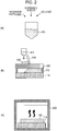
- Figs. 2(a), 2(b) and 2(c) are each a sectional view illustrating a step in the fabrication of a wavelength converting member of the present invention.
- an inorganic binder, a solvent and phosphor particles are provided.
- a preferred inorganic binder may be ethyl silicate obtained by dissolving a silicon precursor into ethanol.
- the inorganic binder may be one obtained by reacting at room temperature or heat treating at a temperature of not more than 500°C a raw material including at least one selected from the group consisting of silicon oxide precursors which form silicon oxide by hydrolysis or oxidation, silicic acid compounds, silica and amorphous silica.
- silicon oxide precursors include those based on perhydropolysilazane, ethyl silicate or methyl silicate.
- the solvent may be a high-boiling solvent such as butanol, isophorone, terpineol or glycerol.
- the phosphor particles may be particles of YAG, LAG and the like. The types and amounts of the phosphor particles are controlled depending on the target illumination light in association with the source light. When, for example, white light is to be obtained from blue light, appropriate amounts of particles of phosphors that are excited by blue light to emit green light and red or yellow light are selected.
- the inorganic binder, the solvent and the phosphor particles are mixed with each other to give a paste (an ink) 410.
- the mixing may be performed with a device such as a ball mill.
- a substrate made of an inorganic material is provided.
- the substrate may be aluminum.
- the substrate is preferably in the form of a sheet.
- a transmission-type wavelength converting member may be fabricated by using such a substrate as glass, sapphire or the like.
- the paste 410 is applied onto the substrate 110 by a screen printing method so that the film thickness will have a ratio to the average particle size in the range described in the table hereinabove.
- the screen printing may be performed by squeezing the paste 410 through a framed silk screen 520 with use of an ink squeegee 510.
- the paste may be applied by spraying, dispenser drawing or inkjetting.
- a screen printing method is preferable in order to form a thin phosphor layer stably.
- the printed paste 410 is then dried and is heat treated in a furnace 600 to evaporate the solvent as well as to drive off the organic matter in the inorganic binder and to oxidize the predominant metal in the inorganic binder (when the predominant metal is Si, to convert the metal into SiO 2 ) while performing bonding of the phosphor layer 120 with the substrate 110.
- a wavelength converting member can be thus obtained.
- a light-emitting device may be fabricated by appropriately arranging a wavelength converting member which has a substrate suited for reflection, with respect to a light source such as an LED.
- wavelength converting members were fabricated as described below.
- a paste prepared by mixing ethyl silicate and terpineol with YAG phosphor particles (average particle size 18 ⁇ m) was applied to sheets made of glass, sapphire and aluminum as substrates by a screen printing method so that the film thickness would be 40 ⁇ m, and the wet films were heat treated. Sample wavelength converting members were thus obtained.
- Figs. 3(a) and 3(b) are sectional views illustrating transmission-type and reflection-type evaluation systems 700 and 800, respectively, for the evaluation of wavelength converting members.
- the transmission-type evaluation system 700 is composed of a light source 710, a plane-convex lens 720, a double-convex lens 730, a band-pass filter 735 and a power meter 740.
- the band-pass filter 735 is a filter that blocks light with wavelengths of 480 nm and below, and is disposed between the double-convex lens and the power meter in the measurement of the fluorescent emission intensity in order to screen out the source light (excitation light) that has passed through the sample, from the fluorescent light.
- the source light that has entered into the plane-convex lens 720 is condensed to a focus on the wavelength converting member 100.
- the radiation emitted from the wavelength converting member 100 is gathered by the double-convex lens 730, and the gathered light is filtered to screen out components with wavelengths of 480 nm and less, and the intensity of the remainder light is measured with the power meter 740.
- the value measured is the fluorescent emission intensity.
- the reflection-type evaluation system 800 includes the same features as the evaluation system 700 except that the features are arranged so that light reflected from the wavelength converting member 100 can be gathered and measured.
- the wavelength converting members were evaluated using the above two types of evaluation systems 700 and 800 appropriately.
- the transmission-type evaluation system 700 was used for those samples having a glass or sapphire substrate, and the reflection-type evaluation system 800 was used for those samples having an aluminum substrate.
- the fluorescent emission intensity is the relative intensity obtained by converting to dimensionless the value shown on a luminance meter during the measurement with the above evaluation system.
- the emission efficiency retention ratio is the ratio of the emission efficiency at a given laser power density to the emission efficiency at a low laser power density where the influence of heat generation and heat storage is negligible, taken as 100%.
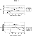
- Figs. 4(a) and 4(b) are each a graph illustrating the emission characteristics obtained while changing the substrates. It has been shown that the fluorescent emission intensity is increased substantially proportionally with the increase in power density up to a certain laser power density with the 3 types of substrates. The emission decreased at laser power densities of 48 W/mm 2 and above for the sapphire substrate, at laser power densities of 27 W/mm 2 and above for the aluminum substrate, and at laser power densities of 11 W/mm 2 and above for the glass substrate.
- Phosphor particles are thermally quenched by an increase in temperature and decrease their luminescent performance.
- Aluminum has higher thermal conductivity than glass. Thus, the reason for the above results is probably because the aluminum substrate prevented the heat generated by the phosphor particles from being stored in the wavelength converting member and consequently the quenching of the phosphor was suppressed.
- quenching was suppressed to a greater degree by the sapphire substrate than by the aluminum substrate having high thermal conductivity.
- the reason for this is probably because in the measurement of the transmissive sapphire substrate, the laser light was applied through the substrate and the heat stored in the phosphor was quickly released to the substrate. Quenching was suppressed to a greater degree by the sapphire substrate than by the aluminum substrate having high thermal conductivity. The reason for this is probably because in the measurement of the transmissive sapphire substrate, the laser light was applied through the substrate and the heat stored in the phosphor was quickly released to the substrate.
- a paste prepared by mixing ethyl silicate and terpineol with YAG-based phosphor particles (average particle size 18 ⁇ m) was applied to Al + Ag sheets as substrates by a screen printing method so that the film thickness would be 30, 40, 60, 100 and 180 ⁇ m. Sample wavelength converting members were thus obtained.
- the Al + Ag substrates were mainly composed of an Al alloy and an Ag film (MIRO2 SILVER manufactured by Alanod was used).
- the wavelength converting members obtained by the above method of the fabrication of wavelength converting members were irradiated with laser light using the reflection-type evaluation system to examine the fluorescent emission intensity and the emission efficiency retention ratio at various laser power densities.
- Figs. 5(a) and 5(b) are each a graph illustrating the emission characteristics obtained while changing the thickness of the phosphor layer relative to the constant phosphor particle size as described in the table below.
- the graphs show the fluorescent emission intensity and the emission efficiency retention ratio at various laser power densities under the respective conditions.
- the fluorescent emission intensity increases with increasing laser input. It has been also shown that until a saturation point is reached, the fluorescent emission intensity is substantially the same irrespective of the phosphor layer thickness/average particle size ratio, and the emission efficiency retention ratio can stay at a high level as the ratio of the phosphor layer thickness to the average particle size is smaller. Regarding the emission efficiency retention, a smaller ratio of the film thickness of the phosphor layer to the average particle size of the phosphor particles is probably more effective for the prevention of heat storage because the number of contacts among the particles is small.
- a paste prepared by mixing ethyl silicate and terpineol with YAG-based phosphor particles was applied to aluminum sheets (reflection-type type) as substrates by a screen printing method.
- the wavelength converting members obtained by the above method of the fabrication of wavelength converting members were irradiated with laser light using the reflection-type evaluation system 800 to examine the emission efficiency retention ratio at a laser power density of 20 W/mm 2 .
- a phosphor generates more heat with increasing value of laser power density.
- the influence of heat generated by increasing the laser power density was calculated from the slope of a graph at low laser power densities where the influence of heat generation was negligible (the slope of a proportional relationship).
- the ideal value with negligible thermal influence was taken as 100%.
- the luminance (emission efficiency) retention ratio was defined as the value obtained by subtracting the proportion of luminance (emission intensity) decreased due to actual influence of heat from 100%. The samples were accepted when the luminance (emission efficiency) retention ratio was 70% or above, and were rejected when the ratio was below 70%.
- the phosphor temperature when the luminance (emission intensity) has fallen to 70% is estimated to be about 300°C. Even these phosphors generally considered to have high heat resistance gradually start to lower their performance when they are heated to 300°C and above in the air. From the points of view of the safety of illumination devices and the life of the phosphor, it will be therefore appropriate that the luminance (emission efficiency) retention ratio under influence of heat be 70% or above. Thus, 70% was adopted as the criterion between acceptance and rejection of the luminance (emission efficiency) retention ratio.
- YAG 62 80 1.3 99.7 Ex. YAG 62 100 1.6 99.5 Ex. YAG 62 200 3.2 98.5 Ex. YAG 62 300 4.8 78.4 Comp. Ex. YAG 62 400 6.5 25.2 Ex. YAG 85 150 1.8 100.3 Ex. YAG 85 200 2.4 99.8 Ex. YAG 85 400 4.7 80.1 Comp. Ex. YAG 85 450 5.3 23.1
- the reflection-type wavelength converting members have been found to meet the evaluation criterion when the average particle size of the phosphor particles and the ratio of the thickness of the phosphor layer to the average particle size of the phosphor particles are in the ranges described in Table 1.
- a paste prepared by mixing ethyl silicate and terpineol with YAG-based phosphor particles was applied to aluminum sheets as substrates by a screen printing method so that the film thickness would be 30 ⁇ m.
- Three types of phosphor particles with average particle sizes of 6, 13 and 18 ⁇ m were used.
- the wavelength converting members with the aluminum substrate obtained by the above method of the fabrication of wavelength converting members were irradiated with laser light using the reflection-type evaluation system 800 to examine the fluorescent emission intensity and the emission efficiency retention ratio at various laser power densities.
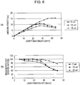
- Figs. 6(a) and 6(b) are each a graph illustrating the emission characteristics obtained while changing the average particle size of the phosphor particles. As illustrated in Figs. 6(a) and 6(b) , it has been shown that the fluorescent emission intensity and the emission efficiency retention ratio are higher with increasing average particle size of the phosphor particles. The reasons for this are probably because the conversion efficiency is higher with increasing size of the phosphor particles and also because larger phosphor particles have less contacts among phosphor particles and consequently thermal storage is prevented.
- a paste prepared by mixing ethyl silicate and terpineol with YAG-based phosphor particles (average particle size 18 ⁇ m) was applied to aluminum sheets as substrates by a screen printing method so that the film thickness would be 30 ⁇ m. Sample wavelength converting members were thus obtained.
- the wavelength converting members obtained were analyzed to calculate the porosity and were subjected to laser irradiation test, and relationships were examined between the porosity and the fluorescent emission intensity and between the porosity and the saturation point.
- the porosity was defined to be the proportion of the volume of pores in the phosphor film relative to the apparent volume obtained by connecting the outermost surfaces of the phosphor particles on the phosphor film with straight lines.
- the volume of the pores was calculated by subtracting the volume of solid components from the apparent volume.
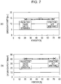
- Figs. 7(a) and 7(b) are graphs illustrating a relationship between the porosity and the fluorescent emission intensity and a relationship between the porosity and the saturation point, respectively. From the relationships of the porosity with the fluorescent emission intensity and the saturation point illustrated in Figs. 7(a) and 7(b) , it has been shown that the fluorescent emission intensity and the saturation point are stable in the range of porosity of 30 to 70%. At a porosity of less than 30%, separation occurs due to the heat treatment during fabrication, and the production of wavelength converting members is difficult. The cause of this separation is probably the difference in thermal expansion between the substrate and the phosphor layer. At a porosity of 70% or above, the phosphor layer hardly maintains its structure and the production is difficult.
- a wavelength converting member (film thickness 30 ⁇ m) of the present invention obtained by the aforementioned method of fabrication of wavelength converting members, and a phosphor plate of a sintered body (a square plate 20.0 mm on a side and 1.0 mm in thickness) were irradiated with laser light using the reflection-type evaluation system 800 to examine the fluorescent emission intensity at various laser power densities and to examine the changes in fluorescent emission intensity depending on the porosity.
- the porosity was defined to be the proportion of the volume of pores in the phosphor film relative to the apparent volume obtained by connecting the outermost surfaces of the phosphor particles on the phosphor film with straight lines.
- the volume of the pores was calculated by subtracting the volume of solid components from the apparent volume.
- the porosity of the wavelength converting member was 40%, and the porosity of the sintered body was less than 1%.
- Figs. 8(a) and 8(b) are each a graph illustrating the emission characteristics of the sintered body and the wavelength converting member.
- Figs. 8(a) and 8(b) have shown that the wavelength converting member has higher fluorescent emission intensity. The reason for this is probably because the light was scattered by the pores in the layer of the wavelength converting member and the phosphor was allowed to convert the light efficiently and attained an increased fluorescent emission intensity.
- the sintered body with less pores is dense and thus it is probable that the laser light is scarcely scattered within the sintered body and simply passes therethrough.
- the wavelength converting member of the present invention that was as thin as 30 ⁇ m scattered the light and emitted fluorescent light with high efficiency by virtue of the presence of appropriate pores. High effectiveness can be thus expected.
Landscapes
- Physics & Mathematics (AREA)
- Chemical & Material Sciences (AREA)
- Engineering & Computer Science (AREA)
- General Physics & Mathematics (AREA)
- Optics & Photonics (AREA)
- Materials Engineering (AREA)
- Organic Chemistry (AREA)
- General Engineering & Computer Science (AREA)
- Electromagnetism (AREA)
- Condensed Matter Physics & Semiconductors (AREA)
- Spectroscopy & Molecular Physics (AREA)
- Inorganic Chemistry (AREA)
- Semiconductor Lasers (AREA)
- Led Device Packages (AREA)
- Luminescent Compositions (AREA)
- Optical Filters (AREA)
Applications Claiming Priority (2)
| Application Number | Priority Date | Filing Date | Title |
|---|---|---|---|
| JP2016011100 | 2016-01-22 | ||
| PCT/JP2017/001078 WO2017126441A1 (fr) | 2016-01-22 | 2017-01-13 | Élément de conversion de longueur d'onde et dispositif électroluminescent |
Publications (3)
| Publication Number | Publication Date |
|---|---|
| EP3407101A1 true EP3407101A1 (fr) | 2018-11-28 |
| EP3407101A4 EP3407101A4 (fr) | 2019-10-09 |
| EP3407101B1 EP3407101B1 (fr) | 2024-05-29 |
Family
ID=59362337
Family Applications (1)
| Application Number | Title | Priority Date | Filing Date |
|---|---|---|---|
| EP17741319.2A Active EP3407101B1 (fr) | 2016-01-22 | 2017-01-13 | Élément de conversion de longueur d'onde et dispositif électroluminescent |
Country Status (7)
| Country | Link |
|---|---|
| US (1) | US10508801B2 (fr) |
| EP (1) | EP3407101B1 (fr) |
| JP (1) | JP6524474B2 (fr) |
| KR (1) | KR102044140B1 (fr) |
| CN (1) | CN108474881B (fr) |
| TW (1) | TWI677115B (fr) |
| WO (1) | WO2017126441A1 (fr) |
Families Citing this family (8)
| Publication number | Priority date | Publication date | Assignee | Title |
|---|---|---|---|---|
| CN208239722U (zh) | 2018-05-24 | 2018-12-14 | 中强光电股份有限公司 | 波长转换轮、照明系统及投影装置 |
| CN110416387B (zh) * | 2019-06-28 | 2020-12-01 | 苏州紫灿科技有限公司 | 一种高散热白光激光片及制备方法 |
| JP7429346B2 (ja) * | 2019-10-03 | 2024-02-08 | 国立研究開発法人物質・材料研究機構 | 波長変換部材 |
| JP2021099415A (ja) * | 2019-12-20 | 2021-07-01 | 日本特殊陶業株式会社 | 波長変換部材および発光装置 |
| JPWO2021221062A1 (fr) * | 2020-04-28 | 2021-11-04 | ||
| CN113917776B (zh) * | 2020-07-09 | 2023-03-24 | 中强光电股份有限公司 | 波长转换装置以及投影装置 |
| EP4286901A4 (fr) * | 2021-01-28 | 2025-01-01 | Niterra Co., Ltd. | Élément de conversion de longueur d'onde et dispositif de source de lumière pourvu de celui-ci |
| WO2022251195A1 (fr) * | 2021-05-24 | 2022-12-01 | W. L. Gore & Associates, Inc. | Composites photoluminescents et leurs procédés de fabrication |
Family Cites Families (20)
| Publication number | Priority date | Publication date | Assignee | Title |
|---|---|---|---|---|
| JP5401772B2 (ja) * | 2003-12-22 | 2014-01-29 | 日亜化学工業株式会社 | 発光装置 |
| JP4960645B2 (ja) * | 2006-03-30 | 2012-06-27 | 京セラ株式会社 | 波長変換器および発光装置 |
| US9631782B2 (en) * | 2010-02-04 | 2017-04-25 | Xicato, Inc. | LED-based rectangular illumination device |
| EP2581943A1 (fr) | 2010-06-11 | 2013-04-17 | Asahi Glass Company, Limited | Stratifié translucide et module de cellule solaire utilisant celui-ci |
| JP2012185403A (ja) * | 2011-03-07 | 2012-09-27 | Seiko Epson Corp | 発光素子とその製造方法、光源装置、およびプロジェクター |
| WO2013001707A1 (fr) * | 2011-06-29 | 2013-01-03 | パナソニック株式会社 | Procédé de fabrication d'élément d'émission lumineuse et dispositif de fabrication d'élément d'émission lumineuse |
| TWI523278B (zh) * | 2011-08-05 | 2016-02-21 | 晶元光電股份有限公司 | 波長轉換結構及其製造方法以及包含此波長轉換結構之發光裝置 |
| TWI505515B (zh) * | 2011-08-19 | 2015-10-21 | Epistar Corp | 發光裝置及其製造方法 |
| JPWO2013051281A1 (ja) | 2011-10-07 | 2015-03-30 | コニカミノルタ株式会社 | Led装置の製造方法、およびそれに用いる蛍光体分散液 |
| WO2013129477A1 (fr) * | 2012-02-27 | 2013-09-06 | 三菱化学株式会社 | Élément de conversion de longueur d'onde et dispositif d'émission de lumière à semi-conducteurs l'utilisant |
| JP6069890B2 (ja) * | 2012-05-29 | 2017-02-01 | 日亜化学工業株式会社 | 波長変換用無機成形体及び発光装置 |
| JP5966529B2 (ja) * | 2012-04-02 | 2016-08-10 | 日亜化学工業株式会社 | 波長変換用無機成形体及び発光装置 |
| CN103367611B (zh) | 2012-03-28 | 2017-08-08 | 日亚化学工业株式会社 | 波长变换用无机成型体及其制造方法以及发光装置 |
| JP2015038960A (ja) * | 2013-05-16 | 2015-02-26 | 株式会社日本セラテック | 発光装置 |
| JP2015065425A (ja) | 2013-08-29 | 2015-04-09 | 株式会社日本セラテック | 発光装置及びその製造方法 |
| JP2015090887A (ja) | 2013-11-05 | 2015-05-11 | 株式会社日本セラテック | 発光素子及び発光装置 |
| JP6232951B2 (ja) | 2013-11-08 | 2017-11-22 | 日本電気硝子株式会社 | プロジェクター用蛍光ホイール、その製造方法及びプロジェクター用発光デバイス |
| JP2015119172A (ja) | 2013-11-13 | 2015-06-25 | 株式会社日本セラテック | 発光素子、発光装置、及びそれらの製造方法 |
| TWI526769B (zh) * | 2013-11-29 | 2016-03-21 | 台達電子工業股份有限公司 | 波長轉換裝置及其製造方法 |
| JP6152801B2 (ja) | 2014-01-21 | 2017-06-28 | 豊田合成株式会社 | 発光装置及びその製造方法 |
-
2017
- 2017-01-13 EP EP17741319.2A patent/EP3407101B1/fr active Active
- 2017-01-13 US US16/070,974 patent/US10508801B2/en active Active
- 2017-01-13 WO PCT/JP2017/001078 patent/WO2017126441A1/fr not_active Ceased
- 2017-01-13 CN CN201780007590.2A patent/CN108474881B/zh active Active
- 2017-01-13 JP JP2017539380A patent/JP6524474B2/ja active Active
- 2017-01-13 KR KR1020187020385A patent/KR102044140B1/ko active Active
- 2017-01-20 TW TW106102006A patent/TWI677115B/zh active
Also Published As
| Publication number | Publication date |
|---|---|
| CN108474881A (zh) | 2018-08-31 |
| TWI677115B (zh) | 2019-11-11 |
| EP3407101B1 (fr) | 2024-05-29 |
| KR20180095645A (ko) | 2018-08-27 |
| EP3407101A4 (fr) | 2019-10-09 |
| WO2017126441A1 (fr) | 2017-07-27 |
| US20190024879A1 (en) | 2019-01-24 |
| JPWO2017126441A1 (ja) | 2018-01-25 |
| KR102044140B1 (ko) | 2019-11-13 |
| US10508801B2 (en) | 2019-12-17 |
| CN108474881B (zh) | 2021-02-02 |
| TW201733170A (zh) | 2017-09-16 |
| JP6524474B2 (ja) | 2019-06-05 |
Similar Documents
| Publication | Publication Date | Title |
|---|---|---|
| EP3407101B1 (fr) | Élément de conversion de longueur d'onde et dispositif électroluminescent | |
| JP6852976B2 (ja) | 波長変換部材、その製造方法および発光装置 | |
| EP3451031B1 (fr) | Élément de conversion de longueur d'onde, son procédé de fabrication, et dispositif électroluminescent | |
| EP3406968B1 (fr) | Élément de conversion de longueur d'onde et dispositif d'émission de lumière | |
| JP6990065B2 (ja) | 波長変換部材、その製造方法および発光装置 | |
| JP2021099415A (ja) | 波長変換部材および発光装置 |
Legal Events
| Date | Code | Title | Description |
|---|---|---|---|
| STAA | Information on the status of an ep patent application or granted ep patent |
Free format text: STATUS: THE INTERNATIONAL PUBLICATION HAS BEEN MADE |
|
| PUAI | Public reference made under article 153(3) epc to a published international application that has entered the european phase |
Free format text: ORIGINAL CODE: 0009012 |
|
| STAA | Information on the status of an ep patent application or granted ep patent |
Free format text: STATUS: REQUEST FOR EXAMINATION WAS MADE |
|
| 17P | Request for examination filed |
Effective date: 20180720 |
|
| AK | Designated contracting states |
Kind code of ref document: A1 Designated state(s): AL AT BE BG CH CY CZ DE DK EE ES FI FR GB GR HR HU IE IS IT LI LT LU LV MC MK MT NL NO PL PT RO RS SE SI SK SM TR |
|
| AX | Request for extension of the european patent |
Extension state: BA ME |
|
| DAV | Request for validation of the european patent (deleted) | ||
| DAX | Request for extension of the european patent (deleted) | ||
| REG | Reference to a national code |
Ref country code: DE Ref legal event code: R079 Free format text: PREVIOUS MAIN CLASS: G02B0005200000 Ipc: C09K0011020000 |
|
| A4 | Supplementary search report drawn up and despatched |
Effective date: 20190909 |
|
| RIC1 | Information provided on ipc code assigned before grant |
Ipc: C09K 11/02 20060101AFI20190903BHEP Ipc: H01L 33/00 20100101ALI20190903BHEP Ipc: C09K 11/77 20060101ALI20190903BHEP Ipc: G02B 5/20 20060101ALI20190903BHEP Ipc: H01S 5/02 20060101ALI20190903BHEP |
|
| STAA | Information on the status of an ep patent application or granted ep patent |
Free format text: STATUS: EXAMINATION IS IN PROGRESS |
|
| 17Q | First examination report despatched |
Effective date: 20220930 |
|
| RAP3 | Party data changed (applicant data changed or rights of an application transferred) |
Owner name: NITERRA CO., LTD. |
|
| GRAP | Despatch of communication of intention to grant a patent |
Free format text: ORIGINAL CODE: EPIDOSNIGR1 |
|
| STAA | Information on the status of an ep patent application or granted ep patent |
Free format text: STATUS: GRANT OF PATENT IS INTENDED |
|
| INTG | Intention to grant announced |
Effective date: 20240118 |
|
| GRAS | Grant fee paid |
Free format text: ORIGINAL CODE: EPIDOSNIGR3 |
|
| GRAA | (expected) grant |
Free format text: ORIGINAL CODE: 0009210 |
|
| STAA | Information on the status of an ep patent application or granted ep patent |
Free format text: STATUS: THE PATENT HAS BEEN GRANTED |
|
| AK | Designated contracting states |
Kind code of ref document: B1 Designated state(s): AL AT BE BG CH CY CZ DE DK EE ES FI FR GB GR HR HU IE IS IT LI LT LU LV MC MK MT NL NO PL PT RO RS SE SI SK SM TR |
|
| REG | Reference to a national code |
Ref country code: CH Ref legal event code: EP |
|
| REG | Reference to a national code |
Ref country code: IE Ref legal event code: FG4D |
|
| REG | Reference to a national code |
Ref country code: DE Ref legal event code: R096 Ref document number: 602017082277 Country of ref document: DE |
|
| REG | Reference to a national code |
Ref country code: NL Ref legal event code: FP |
|
| REG | Reference to a national code |
Ref country code: LT Ref legal event code: MG9D |
|
| PG25 | Lapsed in a contracting state [announced via postgrant information from national office to epo] |
Ref country code: IS Free format text: LAPSE BECAUSE OF FAILURE TO SUBMIT A TRANSLATION OF THE DESCRIPTION OR TO PAY THE FEE WITHIN THE PRESCRIBED TIME-LIMIT Effective date: 20240929 |
|
| PG25 | Lapsed in a contracting state [announced via postgrant information from national office to epo] |
Ref country code: BG Free format text: LAPSE BECAUSE OF FAILURE TO SUBMIT A TRANSLATION OF THE DESCRIPTION OR TO PAY THE FEE WITHIN THE PRESCRIBED TIME-LIMIT Effective date: 20240529 |
|
| PG25 | Lapsed in a contracting state [announced via postgrant information from national office to epo] |
Ref country code: HR Free format text: LAPSE BECAUSE OF FAILURE TO SUBMIT A TRANSLATION OF THE DESCRIPTION OR TO PAY THE FEE WITHIN THE PRESCRIBED TIME-LIMIT Effective date: 20240529 Ref country code: FI Free format text: LAPSE BECAUSE OF FAILURE TO SUBMIT A TRANSLATION OF THE DESCRIPTION OR TO PAY THE FEE WITHIN THE PRESCRIBED TIME-LIMIT Effective date: 20240529 |
|
| PG25 | Lapsed in a contracting state [announced via postgrant information from national office to epo] |
Ref country code: GR Free format text: LAPSE BECAUSE OF FAILURE TO SUBMIT A TRANSLATION OF THE DESCRIPTION OR TO PAY THE FEE WITHIN THE PRESCRIBED TIME-LIMIT Effective date: 20240830 |
|
| REG | Reference to a national code |
Ref country code: AT Ref legal event code: MK05 Ref document number: 1690634 Country of ref document: AT Kind code of ref document: T Effective date: 20240529 |
|
| PG25 | Lapsed in a contracting state [announced via postgrant information from national office to epo] |
Ref country code: ES Free format text: LAPSE BECAUSE OF FAILURE TO SUBMIT A TRANSLATION OF THE DESCRIPTION OR TO PAY THE FEE WITHIN THE PRESCRIBED TIME-LIMIT Effective date: 20240529 |
|
| PG25 | Lapsed in a contracting state [announced via postgrant information from national office to epo] |
Ref country code: AT Free format text: LAPSE BECAUSE OF FAILURE TO SUBMIT A TRANSLATION OF THE DESCRIPTION OR TO PAY THE FEE WITHIN THE PRESCRIBED TIME-LIMIT Effective date: 20240529 |
|
| PG25 | Lapsed in a contracting state [announced via postgrant information from national office to epo] |
Ref country code: PL Free format text: LAPSE BECAUSE OF FAILURE TO SUBMIT A TRANSLATION OF THE DESCRIPTION OR TO PAY THE FEE WITHIN THE PRESCRIBED TIME-LIMIT Effective date: 20240529 |
|
| PG25 | Lapsed in a contracting state [announced via postgrant information from national office to epo] |
Ref country code: LV Free format text: LAPSE BECAUSE OF FAILURE TO SUBMIT A TRANSLATION OF THE DESCRIPTION OR TO PAY THE FEE WITHIN THE PRESCRIBED TIME-LIMIT Effective date: 20240529 |
|
| PG25 | Lapsed in a contracting state [announced via postgrant information from national office to epo] |
Ref country code: PL Free format text: LAPSE BECAUSE OF FAILURE TO SUBMIT A TRANSLATION OF THE DESCRIPTION OR TO PAY THE FEE WITHIN THE PRESCRIBED TIME-LIMIT Effective date: 20240529 Ref country code: NO Free format text: LAPSE BECAUSE OF FAILURE TO SUBMIT A TRANSLATION OF THE DESCRIPTION OR TO PAY THE FEE WITHIN THE PRESCRIBED TIME-LIMIT Effective date: 20240829 Ref country code: LV Free format text: LAPSE BECAUSE OF FAILURE TO SUBMIT A TRANSLATION OF THE DESCRIPTION OR TO PAY THE FEE WITHIN THE PRESCRIBED TIME-LIMIT Effective date: 20240529 Ref country code: IS Free format text: LAPSE BECAUSE OF FAILURE TO SUBMIT A TRANSLATION OF THE DESCRIPTION OR TO PAY THE FEE WITHIN THE PRESCRIBED TIME-LIMIT Effective date: 20240929 Ref country code: HR Free format text: LAPSE BECAUSE OF FAILURE TO SUBMIT A TRANSLATION OF THE DESCRIPTION OR TO PAY THE FEE WITHIN THE PRESCRIBED TIME-LIMIT Effective date: 20240529 Ref country code: GR Free format text: LAPSE BECAUSE OF FAILURE TO SUBMIT A TRANSLATION OF THE DESCRIPTION OR TO PAY THE FEE WITHIN THE PRESCRIBED TIME-LIMIT Effective date: 20240830 Ref country code: FI Free format text: LAPSE BECAUSE OF FAILURE TO SUBMIT A TRANSLATION OF THE DESCRIPTION OR TO PAY THE FEE WITHIN THE PRESCRIBED TIME-LIMIT Effective date: 20240529 Ref country code: ES Free format text: LAPSE BECAUSE OF FAILURE TO SUBMIT A TRANSLATION OF THE DESCRIPTION OR TO PAY THE FEE WITHIN THE PRESCRIBED TIME-LIMIT Effective date: 20240529 Ref country code: BG Free format text: LAPSE BECAUSE OF FAILURE TO SUBMIT A TRANSLATION OF THE DESCRIPTION OR TO PAY THE FEE WITHIN THE PRESCRIBED TIME-LIMIT Effective date: 20240529 Ref country code: AT Free format text: LAPSE BECAUSE OF FAILURE TO SUBMIT A TRANSLATION OF THE DESCRIPTION OR TO PAY THE FEE WITHIN THE PRESCRIBED TIME-LIMIT Effective date: 20240529 Ref country code: RS Free format text: LAPSE BECAUSE OF FAILURE TO SUBMIT A TRANSLATION OF THE DESCRIPTION OR TO PAY THE FEE WITHIN THE PRESCRIBED TIME-LIMIT Effective date: 20240829 |
|
| PG25 | Lapsed in a contracting state [announced via postgrant information from national office to epo] |
Ref country code: DK Free format text: LAPSE BECAUSE OF FAILURE TO SUBMIT A TRANSLATION OF THE DESCRIPTION OR TO PAY THE FEE WITHIN THE PRESCRIBED TIME-LIMIT Effective date: 20240529 |
|
| PG25 | Lapsed in a contracting state [announced via postgrant information from national office to epo] |
Ref country code: EE Free format text: LAPSE BECAUSE OF FAILURE TO SUBMIT A TRANSLATION OF THE DESCRIPTION OR TO PAY THE FEE WITHIN THE PRESCRIBED TIME-LIMIT Effective date: 20240529 |
|
| PG25 | Lapsed in a contracting state [announced via postgrant information from national office to epo] |
Ref country code: CZ Free format text: LAPSE BECAUSE OF FAILURE TO SUBMIT A TRANSLATION OF THE DESCRIPTION OR TO PAY THE FEE WITHIN THE PRESCRIBED TIME-LIMIT Effective date: 20240529 |
|
| PG25 | Lapsed in a contracting state [announced via postgrant information from national office to epo] |
Ref country code: RO Free format text: LAPSE BECAUSE OF FAILURE TO SUBMIT A TRANSLATION OF THE DESCRIPTION OR TO PAY THE FEE WITHIN THE PRESCRIBED TIME-LIMIT Effective date: 20240529 Ref country code: SK Free format text: LAPSE BECAUSE OF FAILURE TO SUBMIT A TRANSLATION OF THE DESCRIPTION OR TO PAY THE FEE WITHIN THE PRESCRIBED TIME-LIMIT Effective date: 20240529 |
|
| PG25 | Lapsed in a contracting state [announced via postgrant information from national office to epo] |
Ref country code: SM Free format text: LAPSE BECAUSE OF FAILURE TO SUBMIT A TRANSLATION OF THE DESCRIPTION OR TO PAY THE FEE WITHIN THE PRESCRIBED TIME-LIMIT Effective date: 20240529 |
|
| PG25 | Lapsed in a contracting state [announced via postgrant information from national office to epo] |
Ref country code: SM Free format text: LAPSE BECAUSE OF FAILURE TO SUBMIT A TRANSLATION OF THE DESCRIPTION OR TO PAY THE FEE WITHIN THE PRESCRIBED TIME-LIMIT Effective date: 20240529 Ref country code: SK Free format text: LAPSE BECAUSE OF FAILURE TO SUBMIT A TRANSLATION OF THE DESCRIPTION OR TO PAY THE FEE WITHIN THE PRESCRIBED TIME-LIMIT Effective date: 20240529 Ref country code: RO Free format text: LAPSE BECAUSE OF FAILURE TO SUBMIT A TRANSLATION OF THE DESCRIPTION OR TO PAY THE FEE WITHIN THE PRESCRIBED TIME-LIMIT Effective date: 20240529 Ref country code: EE Free format text: LAPSE BECAUSE OF FAILURE TO SUBMIT A TRANSLATION OF THE DESCRIPTION OR TO PAY THE FEE WITHIN THE PRESCRIBED TIME-LIMIT Effective date: 20240529 Ref country code: DK Free format text: LAPSE BECAUSE OF FAILURE TO SUBMIT A TRANSLATION OF THE DESCRIPTION OR TO PAY THE FEE WITHIN THE PRESCRIBED TIME-LIMIT Effective date: 20240529 Ref country code: CZ Free format text: LAPSE BECAUSE OF FAILURE TO SUBMIT A TRANSLATION OF THE DESCRIPTION OR TO PAY THE FEE WITHIN THE PRESCRIBED TIME-LIMIT Effective date: 20240529 |
|
| PG25 | Lapsed in a contracting state [announced via postgrant information from national office to epo] |
Ref country code: IT Free format text: LAPSE BECAUSE OF FAILURE TO SUBMIT A TRANSLATION OF THE DESCRIPTION OR TO PAY THE FEE WITHIN THE PRESCRIBED TIME-LIMIT Effective date: 20240529 |
|
| REG | Reference to a national code |
Ref country code: DE Ref legal event code: R097 Ref document number: 602017082277 Country of ref document: DE |
|
| PLBE | No opposition filed within time limit |
Free format text: ORIGINAL CODE: 0009261 |
|
| STAA | Information on the status of an ep patent application or granted ep patent |
Free format text: STATUS: NO OPPOSITION FILED WITHIN TIME LIMIT |
|
| PG25 | Lapsed in a contracting state [announced via postgrant information from national office to epo] |
Ref country code: SI Free format text: LAPSE BECAUSE OF FAILURE TO SUBMIT A TRANSLATION OF THE DESCRIPTION OR TO PAY THE FEE WITHIN THE PRESCRIBED TIME-LIMIT Effective date: 20240529 |
|
| 26N | No opposition filed |
Effective date: 20250303 |
|
| REG | Reference to a national code |
Ref country code: CH Ref legal event code: PL |
|
| PG25 | Lapsed in a contracting state [announced via postgrant information from national office to epo] |
Ref country code: SE Free format text: LAPSE BECAUSE OF FAILURE TO SUBMIT A TRANSLATION OF THE DESCRIPTION OR TO PAY THE FEE WITHIN THE PRESCRIBED TIME-LIMIT Effective date: 20240529 |
|
| PG25 | Lapsed in a contracting state [announced via postgrant information from national office to epo] |
Ref country code: MC Free format text: LAPSE BECAUSE OF FAILURE TO SUBMIT A TRANSLATION OF THE DESCRIPTION OR TO PAY THE FEE WITHIN THE PRESCRIBED TIME-LIMIT Effective date: 20240529 Ref country code: LU Free format text: LAPSE BECAUSE OF NON-PAYMENT OF DUE FEES Effective date: 20250113 |
|
| GBPC | Gb: european patent ceased through non-payment of renewal fee |
Effective date: 20250113 |
|
| PG25 | Lapsed in a contracting state [announced via postgrant information from national office to epo] |
Ref country code: BE Free format text: LAPSE BECAUSE OF NON-PAYMENT OF DUE FEES Effective date: 20250131 Ref country code: GB Free format text: LAPSE BECAUSE OF NON-PAYMENT OF DUE FEES Effective date: 20250113 |
|
| PG25 | Lapsed in a contracting state [announced via postgrant information from national office to epo] |
Ref country code: FR Free format text: LAPSE BECAUSE OF NON-PAYMENT OF DUE FEES Effective date: 20250131 |
|
| PG25 | Lapsed in a contracting state [announced via postgrant information from national office to epo] |
Ref country code: CH Free format text: LAPSE BECAUSE OF NON-PAYMENT OF DUE FEES Effective date: 20250131 |
|
| REG | Reference to a national code |
Ref country code: BE Ref legal event code: MM Effective date: 20250131 |
|
| PGFP | Annual fee paid to national office [announced via postgrant information from national office to epo] |
Ref country code: NL Payment date: 20251215 Year of fee payment: 10 |
|
| PG25 | Lapsed in a contracting state [announced via postgrant information from national office to epo] |
Ref country code: IE Free format text: LAPSE BECAUSE OF NON-PAYMENT OF DUE FEES Effective date: 20250113 |
|
| PGFP | Annual fee paid to national office [announced via postgrant information from national office to epo] |
Ref country code: DE Payment date: 20251203 Year of fee payment: 10 |
|
| PG25 | Lapsed in a contracting state [announced via postgrant information from national office to epo] |
Ref country code: PT Free format text: LAPSE BECAUSE OF NON-PAYMENT OF DUE FEES Effective date: 20240529 |