EP3407116A1 - Elément optique, dispositif d'affichage utilisant celui-ci, et dispositif de réception de lumière - Google Patents
Elément optique, dispositif d'affichage utilisant celui-ci, et dispositif de réception de lumière Download PDFInfo
- Publication number
- EP3407116A1 EP3407116A1 EP16886235.7A EP16886235A EP3407116A1 EP 3407116 A1 EP3407116 A1 EP 3407116A1 EP 16886235 A EP16886235 A EP 16886235A EP 3407116 A1 EP3407116 A1 EP 3407116A1
- Authority
- EP
- European Patent Office
- Prior art keywords
- light
- beam splitter
- substrate
- image display
- luminous flux
- Prior art date
- Legal status (The legal status is an assumption and is not a legal conclusion. Google has not performed a legal analysis and makes no representation as to the accuracy of the status listed.)
- Granted
Links
Images






Classifications
-
- G—PHYSICS
- G02—OPTICS
- G02B—OPTICAL ELEMENTS, SYSTEMS OR APPARATUS
- G02B27/00—Optical systems or apparatus not provided for by any of the groups G02B1/00 - G02B26/00, G02B30/00
- G02B27/0081—Optical systems or apparatus not provided for by any of the groups G02B1/00 - G02B26/00, G02B30/00 with means for altering, e.g. enlarging, the entrance or exit pupil
-
- G—PHYSICS
- G02—OPTICS
- G02B—OPTICAL ELEMENTS, SYSTEMS OR APPARATUS
- G02B17/00—Systems with reflecting surfaces, with or without refracting elements
- G02B17/08—Catadioptric systems
-
- G—PHYSICS
- G02—OPTICS
- G02B—OPTICAL ELEMENTS, SYSTEMS OR APPARATUS
- G02B27/00—Optical systems or apparatus not provided for by any of the groups G02B1/00 - G02B26/00, G02B30/00
- G02B27/01—Head-up displays
- G02B27/017—Head mounted
- G02B27/0172—Head mounted characterised by optical features
-
- G—PHYSICS
- G02—OPTICS
- G02B—OPTICAL ELEMENTS, SYSTEMS OR APPARATUS
- G02B27/00—Optical systems or apparatus not provided for by any of the groups G02B1/00 - G02B26/00, G02B30/00
- G02B27/02—Viewing or reading apparatus
-
- G—PHYSICS
- G02—OPTICS
- G02B—OPTICAL ELEMENTS, SYSTEMS OR APPARATUS
- G02B6/00—Light guides; Structural details of arrangements comprising light guides and other optical elements, e.g. couplings
-
- G—PHYSICS
- G02—OPTICS
- G02B—OPTICAL ELEMENTS, SYSTEMS OR APPARATUS
- G02B6/00—Light guides; Structural details of arrangements comprising light guides and other optical elements, e.g. couplings
- G02B6/0001—Light guides; Structural details of arrangements comprising light guides and other optical elements, e.g. couplings specially adapted for lighting devices or systems
- G02B6/0011—Light guides; Structural details of arrangements comprising light guides and other optical elements, e.g. couplings specially adapted for lighting devices or systems the light guides being planar or of plate-like form
- G02B6/0033—Means for improving the coupling-out of light from the light guide
- G02B6/005—Means for improving the coupling-out of light from the light guide provided by one optical element, or plurality thereof, placed on the light output side of the light guide
- G02B6/0055—Reflecting element, sheet or layer
-
- G—PHYSICS
- G02—OPTICS
- G02C—SPECTACLES; SUNGLASSES OR GOGGLES INSOFAR AS THEY HAVE THE SAME FEATURES AS SPECTACLES; CONTACT LENSES
- G02C7/00—Optical parts
-
- G—PHYSICS
- G02—OPTICS
- G02C—SPECTACLES; SUNGLASSES OR GOGGLES INSOFAR AS THEY HAVE THE SAME FEATURES AS SPECTACLES; CONTACT LENSES
- G02C7/00—Optical parts
- G02C7/02—Lenses; Lens systems ; Methods of designing lenses
- G02C7/08—Auxiliary lenses; Arrangements for varying focal length
- G02C7/086—Auxiliary lenses located directly on a main spectacle lens or in the immediate vicinity of main spectacles
-
- H—ELECTRICITY
- H04—ELECTRIC COMMUNICATION TECHNIQUE
- H04N—PICTORIAL COMMUNICATION, e.g. TELEVISION
- H04N5/00—Details of television systems
- H04N5/64—Constructional details of receivers, e.g. cabinets or dust covers
-
- G—PHYSICS
- G02—OPTICS
- G02B—OPTICAL ELEMENTS, SYSTEMS OR APPARATUS
- G02B27/00—Optical systems or apparatus not provided for by any of the groups G02B1/00 - G02B26/00, G02B30/00
- G02B27/01—Head-up displays
- G02B27/017—Head mounted
- G02B2027/0178—Eyeglass type
Definitions
- the present invention relates to an optical element for propagating light in a set direction, and to a display device and photoreceptor device using such an optical element, relating in particular to a display device suitable for monitors for information appliances that can be used outside of a desktop environment, such as wearable computers which are worn on the body by means of a waist belt, personal accessories and the like, and communication devices such as portable telephones which can be carried by placing in a knapsack or pocket.
- FIG. 3 is an external view showing a goggle type display (display device) worn by a viewer
- FIG. 4 is a drawing illustrating the general configuration of a conventional goggle type display and the optical path in the XY plane.
- the goggle type display 101 is for the right eye, and defines an XYZ coordinate system having its origin at the center of the right eye E of a viewer viewing into the distance.
- the Y direction is to the front of the viewer, the Z direction is above the viewer, and the X direction (set direction) is to the left of the viewer.
- the goggle type display 101 has an appearance similar to goggles, and comprises an output unit (output optical system) 40 which outputs image display light L, a light guide (optical element) 10 which is a substrate that internally reflects the image display light L from the output unit 40 and guides it to the eye E of the viewer, and a frame part F to which the output unit 40 and light guide 10 are attached (for example, see patent literature 1).
- the output unit 40 has a housing as shown in FIG. 3 , and inside this housing, comprises an output mechanism including a transmissive liquid crystal display 41, an optical system 42 and a light source (not illustrated), and a control unit (not illustrated) which outputs an image signal to the output mechanism.
- an output mechanism including a transmissive liquid crystal display 41, an optical system 42 and a light source (not illustrated), and a control unit (not illustrated) which outputs an image signal to the output mechanism.
- the transmissive liquid crystal display 41 based on an image signal from the control unit, forms an image in a display region perpendicular to the output direction, and outputs an image display light L.
- Optical system 42 transmits the image display light L of the display region.
- Optical system 42 is furthermore arranged at a distance in front of the transmissive liquid crystal display 41. As a result, the optical system 42 forms a virtual image of the observed object while transmitting image display light L of the display region.
- Light guide 10 is a substrate fashioned from a light transmitting material such as glass (BK7, etc.), resin (polycarbonate, polymethacrylic acid (PMMA), cycloolefin, etc.) or the like and comprises a front surface 10a, a rear surface 10b located opposite the front surface 10a in the -Y direction, a right surface 10c, a left surface 10d located opposite the right surface 10c in the X direction, a top surface (not illustrated) and a bottom surface (not illustrated) located opposite the top surface in the Z direction, and furthermore has a beam splitter surface 11 formed inside.
- the front surface 10a, the rear surface 10b, the top surface and the bottom surface are parallel to the X direction (set direction), while the left surface 10d is perpendicular to the X direction (set direction).
- the right surface 10c is arranged so as to have an angle ⁇ to the X direction (set direction) when viewed from the Z direction.
- the output unit 40 is moreover arranged so as to cause the image display light L from the output mechanism to be inputted through the right surface 10c of the light guide 10 into the light guide 10 in a direction perpendicular to the right surface 10c.
- image display light L from the output unit 40 enters inside the light guide 10 through the right surface 10c in a direction perpendicular to the right surface 10c, it advances substantially in the X direction (set direction).
- the beam splitter surface 11 comprises three planar beam splitter surfaces, arranged in the X direction in the sequence: first beam splitter surface 11a, second beam splitter surface 11b, third beam splitter surface 11c. Furthermore, each of the beam splitter surfaces 11a through 11c are arranged at the same angle ⁇ to the X direction when viewed from the Z direction.
- the first beam splitter surface 11a, second beam splitter surface 11b and third beam splitter surface 11c furthermore make it possible to reflect a predetermined fraction of the luminous flux of the inputted image display light L and to transmit a predetermined fraction of the luminous flux of the image display light L.
- the image display light L of the display region from the output unit 40 is inputted into the light guide 10 through the right surface 10c.
- the image display light L from the output unit 40 is inputted through the right surface 10c into the light guide 10 in a direction perpendicular to the right surface 10c, and the right surface 10c causes the image display light L of the display region from the output unit 40 to be inputted such that it advances substantially in the X direction (set direction).
- the front surface 10a and rear surface 10b cause the image display light L of the display region to advance in the X direction (set direction) while reflecting it in alternation multiple times, thereby leading it to the first beam splitter surface 11a.
- the first beam splitter surface 11a then reflects a predetermined fraction of the luminous flux of the inputted image display light L and transmits a predetermined fraction of the luminous flux of the image display light L. Namely, the luminous flux of image display light La is guided to the eye E of the viewer.
- the image display light L which has passed through the first beam splitter surface 11a reaches the second beam splitter surface 11b.
- the second beam splitter surface 11b reflects a predetermined fraction of the luminous flux of the inputted image display light L and transmits a predetermined fraction of the luminous flux of the image display light L. Namely, the luminous flux of image display light Lb is guided to the eye E of the viewer.
- the image display light L which has passed through the second beam splitter surface 11b reaches the third beam splitter surface 11c.
- the third beam splitter surface 11c reflects a predetermined fraction of the luminous flux of the inputted image display light L and transmits a predetermined fraction of the luminous flux of the image display light L. Namely, the luminous flux of image display light Lc is guided to the eye E of the viewer.
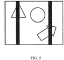
- FIG. 5 is an example of an image in which a shadow seen by the viewer has been generated by the goggle type display 101 of FIG. 4 .
- the present applicant investigated methods that would allow the viewer to properly see the image, and found that in a goggle type display 101 as described above, the size of the luminous flux of the image display light L (the display region) is limited by the size of the right surface 10c, and with a luminous flux size that has been limited by the size of the right surface 10c shown in FIG. 4 , regions occur in which luminous flux of image display light L propagating through the inside of the light guide 10 is not present (dropouts).
- FIG. 6 is a drawing illustrating the propagation range of luminous flux in the XY plane of the goggle type display 101 of FIG. 4 , where symbols A in the drawing indicate luminous flux dropouts.
- FIG. 7 is a plan view illustrating a light guide in which the size of the right surface and the size of the light flux have been increased.
- this sort of light guide 300 has protruding parts and is thus difficult to manufacture and also makes the output unit 340 larger and heavier.
- Japanese Unexamined Patent Application Publication 2011-164545 discloses a display device comprising a first light guide for guiding image display light from a first output unit and a second light guide for guiding image display light from a second output unit, but since this device comprises two output units, it has the problem that it becomes larger and heavier.
- International Publication No. WO2011/24291 discloses a display device comprising a first light guide which reflects image display light by means of four surfaces - a front surface, rear surface, top surface and bottom surface, in order to guide it to a second light guide, and a second light guide for guiding the image display light from the first light guide, but this has the problem of making the device large and heavy.
- the applicant discovered how to arrange a substance (secondary substrate) across a beam splitter surface (secondary beam splitter) in front of the light guide (main substrate) in order to prevent dropouts of luminous flux of the image display light propagating through the inside of the light guide without providing protruding parts as in light guide 300 and without increasing the size of the output unit 340, etc.
- beam splitter surface here refers to a surface having the function of reflecting a portion of the luminous flux and transmitting a portion of the luminous flux.
- the image display light of the display region is reflected in alternation multiple time at the front surface and rear surface of the light guide, and when it reaches the front surface (secondary beam splitter surface) of the light guide, 100% of the luminous flux of the image display light is not reflected, but rather a predetermined fraction of the luminous flux of the image display light is reflected and advances into the light guide, and a predetermined fraction of the luminous flux of the image display light is transmitted and advances into the secondary substrate.
- a difference occurs between the optical path of the image display light advancing inside the light guide and the optical path of the image display light advancing inside the secondary substrate (the image display light is split by the secondary beam splitter surface and is magnified), and the occurrence of regions where luminous flux of image display light propagating through the inside of the light guide is not present (dropouts) can be prevented by making use of this difference (offset).
- the optical element of the present invention comprises a main substrate fabricated from light transmitting material, whereof the front surface and rear surface are parallel to a set direction, and having at least one main beam splitter surface formed diagonally to the set direction inside the main substrate, which optical element further comprises a secondary substrate fabricated from light transmitting material, whereof the front surface and rear surface are parallel to a set direction, wherein a secondary beam splitter surface is arranged between the front surface of the secondary substrate and the rear surface of said main substrate or between the rear surface of the secondary substrate and the front surface of said main substrate.
- set direction is an arbitrary direction determined in advance by the designer, etc., and could be, for example, the left direction, right direction, top direction or bottom direction.
- optical element of the present invention As described above, light is split and magnified by a secondary beam splitter surface, thus making it possible to prevent the occurrence of regions where luminous flux propagating through the inside of the main substrate is not present (dropouts).
- light may be inputted or outputted through a surface other than the front surface and rear surface of the main substrate and the front surface and rear surface of the secondary substrate.
- the optical element of the present invention when the right surface, etc. of the secondary substrate is formed diagonally, the concentration of complex processing on a single substrate can be avoided, so productivity is improved. Furthermore, when the width of the output mechanism is to be reduced, in the case where the image display light is inputted through the right surface of the main substrate, if the main substrate is made thinner, it is necessary to increase the number of main beam splitter surfaces in the main substrate in order to maintain the output range outputted by the main beam splitter surface, but by inputting the image display light through the right surface, etc. of the secondary substrate, the need to increase the number of main beam splitter surfaces of the main substrate is eliminated even if the secondary substrate is made thinner, so productivity is better.
- a reflective surface may be formed inside the main substrate or the secondary substrate, so that light enters through at least one surface from among the front surface and rear surface of the main substrate and the front surface and rear surface of the secondary substrate and either reaches the reflective surface or, after reaching the reflective surface, is outputted from at least one surface from among the front surface and rear surface of the main substrate and the front surface and rear surface of the secondary substrate.
- the optical element of the present invention makes it possible to increase the degree of freedom in respect of the location where light enters inside the main substrate and secondary substrate and the location where it is outputted from inside the main substrate and secondary substrate.
- the secondary beam splitter surface may be arranged so that light is not reflected two or more times from the reflective surface.
- a substrate of a fixed minimum thickness is arranged in front of the reflective surface, so luminous flux which is reflected two or more times from the reflective surface can be eliminated and the occurrence of stray light can be prevented.
- the display device of the present invention may comprise an optical element as described above and an output optical system which outputs light.
- regions where luminous flux is not present do not occur and the output mechanism can be made smaller and lighter.
- the difference between the light quantity outputted to the outside from the first main beam splitter surface near the input location and the light quantity outputted to the outside from the Nth main beam splitter surface from the input location becomes smaller, making it possible to make the brightness (light quantity) more uniform.
- the photoreceptor device of the present invention may comprise an optical element as described above and a photoreceptor optical system which detects light.
- the photoreceptor device of the present invention is able to sense objects of sensing located in any region of the luminous flux.
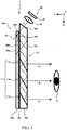
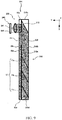
- FIG. 1 is a drawing illustrating the general configuration and optical path in the XY plane of a goggle type display (display device) of the present invention
- FIG. 2 is drawing illustrating the propagation range of luminous flux in FIG. 1 . Similar parts have been assigned the same reference symbols as in goggle type display 101 described above.
- the goggle type display 1 has an appearance similar to goggles, and comprises an output unit 40 which outputs image display light L, a light guide (optical element) 100 which internally reflects the image display light L from the output unit 40 and guides it to the eye E of the viewer, and a frame part F to which the output unit 40 and light guide 100 are attached.
- the light guide unit 100 comprises a main substrate 10 with a main beam splitter surface 11 formed inside, a secondary substrate 20, and a secondary beam splitter surface 30.
- the secondary substrate 20 has a front surface 20a, a rear surface 20b located opposite the front surface 20a in the -Y direction, a right surface 20c, a left surface 20d located opposite the right surface 20c in the X direction, a top surface (not illustrated), and a bottom surface (not illustrated) located opposite the top surface in the Z direction.
- the front surface 20a and rear surface 20b are parallel to the X direction (set direction). Namely, the front surface 10a, rear surface 10b, front surface 20a and rear surface 20b are parallel to the X direction (set direction).
- the gap between the front surface 20a and the rear surface 20b is a prescribed distance (thickness) determined by the designer using calculation formulas, simulation software and the like in consideration of the difference (offset) between the optical path of the image display light L which advances inside the main substrate 10 and the optical path of the image display light L which advances inside the secondary substrate 20, so that dropouts of luminous flux propagating inside the main substrate 10 do not occur.
- the material of the secondary substrate includes light transmitting materials such as glass (BK7), resin (polycarbonate, polymethacrylic acid (PMMA), cycloolefin, etc.) or the like, where from the standpoint of ease of manufacturing, change in response to temperature, etc., glass is preferable, and from the standpoint of safety, such as resistance to breaking during use, polycarbonate is preferable.
- glass glass
- resin polycarbonate, polymethacrylic acid (PMMA), cycloolefin, etc.
- the secondary beam splitter surface 30 makes it possible to reflect a set fraction of the luminous flux of inputted image display light L and to transmit a set fraction of the luminous flux of the image display light L.
- the set fractions of light reflected and transmitted by the secondary beam splitter surface are fractions set by the designer using calculation formulas, simulation software and the like, so that the brightness of the area where dropouts of luminous flux propagating inside the main substrate 10 have been eliminated will be more uniform with the brightness of the other areas, being preferably 20% or greater and 80% or less, for example, 50%, etc.
- the secondary beam splitter surface 30 may be formed for example on the rear surface 20b of the secondary substrate 20 through optical coating, with the front surface 10a of the main substrate 10 being bonded to the rear surface 20b of the secondary substrate 20, which is preferable from the standpoint of facilitating fixation of the elements, and moreover may be arranged between the front surface 10a of the main substrate 10 and the rear surface 20b of the secondary substrate 20 by being directly bonded (optical contact, anodic bonding, diffusion bonding, ambient temperature bonding, thermal bonding, fluoric acid bonding, etc.), which is preferable from the standpoint of eliminating the need for adhesive with a predetermined refractive index.
- the secondary beam splitter surface 30 may be formed by making use of reflection occurring due to a combination of materials of different refractive indices for the main substrate 10 and secondary substrate 20, and may also be formed by filling the space between the main substrate 10 and secondary substrate 20 with a medium such as adhesive, air or oil, and making use of reflection generated due to the difference between the refractive index of that medium and the refractive index of the main substrate 10 and secondary substrate 20.
- image display light L of the display region from the output unit 40 is inputted inside the main substrate 10 through the right surface 10c.
- the image display light L from the output unit 40 is inputted inside through the right surface 10c in a direction perpendicular to the right surface 10c, and the right surface 10c causes the image display light L of the display region from the output unit 40 to be inputted such that it advances substantially in the X direction (set direction).
- the front surface 10a and rear surface 10b reflect the image display light L of the display region multiple times in alternation, causing it to advance in the X direction (set direction).
- the advancing image display light L reaches the secondary beam splitter surface 30 (front surface 10a), and the secondary beam splitter surface 30 (front surface 10a) reflects a set fraction of the luminous flux of the inputted image display light L and transmits a set fraction of the luminous flux of the image display light L.
- the image display light L reaches the secondary beam splitter surface 30 (front surface 10a)
- a set fraction of the luminous flux of the image display light L advances inside the main substrate 10
- a set fraction of the luminous flux of the image display light L advances inside the secondary substrate 20.
- the image display light L which has advanced inside the secondary substrate 20 is reflected by the front surface 20a and then reaches the secondary beam splitter surface 30 (front surface 10a).
- the secondary beam splitter surface 30 (front surface 10a) reflects a set fraction of the luminous flux of the inputted image display light L and transmits a set fraction of the luminous flux of the image display light L.
- a set fraction of the luminous flux of the image display light L advances inside the main substrate 10 and a set fraction of the luminous flux of the image display light L advances through the inside of the secondary substrate 20.
- the image display light L which has advanced through the inside of the main substrate 10 or the secondary substrate 20 reaches the first main beam splitter surface 11a.
- the first main beam splitter surface 11a reflects a prescribed fraction of the luminous flux of the inputted image display light L and transmits a prescribed fraction of the luminous flux of the image display light L. Namely, the luminous flux of image display light La is guided toward the viewer.
- the image display light L which has been transmitted through the first main beam splitter surface 11a or which has advanced through the inside of the secondary substrate 20 reaches the second main beam splitter surface 11b.
- the second main beam splitter surface 11b reflects a prescribed fraction of the luminous flux of the inputted image display light L and transmits a prescribed fraction of the luminous flux of the image display light L. Namely, the luminous flux of image display light Lb is guided toward the viewer.
- image display light L which has been transmitted through the first main beam splitter surface 11a or through the second main beam splitter surface 11b or which has advanced through the inside of the secondary substrate 20 reaches the third main beam splitter surface 11c.
- the third main beam splitter surface 11c reflects a prescribed fraction of the luminous flux of the inputted image display light L and transmits a prescribed fraction of the luminous flux of the image display light L. Namely, the luminous flux of image display light Lc is guided toward the viewer.
- the image display light L is split and magnified by the secondary beam splitter surface 30, making it possible to prevent the occurrence of regions where luminous flux propagating through the inside of the main substrate 10 is not present (dropouts). Furthermore, since the secondary substrate 20 is bonded to the front surface 10a of the main substrate 10, the overall strength of the light guide unit 100 is improved.
- image display light L advances in the X direction (set direction)
- image display light L since there exists image display light L which passes through the inside of the secondary substrate 20 without being transmitted through the main beam splitter surfaces 11a and 11b, the difference between the light quantity outputted to the outside from the first main beam splitter surface 11a and the light quantity outputted to the outside from the third main beam splitter surface 11c becomes smaller, allowing the brightness (light quantity) to be made more uniform.
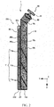
- FIG. 8 is a drawing illustrating the general configuration and optical path in the XY plane of a goggle type display (display device) of the present invention
- FIG. 9 is a drawing illustrating the propagation range of luminous flux in FIG. 8 . Similar parts have been assigned the same reference symbols as in goggle type display 1 described above.
- the goggle type display 201 has an appearance similar to goggles, and comprises an output unit 240 which outputs image display light L, a light guide unit (optical element) 200 which internally reflects the image display light L from the output unit 240 and guides it to the eye E of the viewer, and a frame part F to which the output unit 240 and light guide 200 are attached.
- an output unit 240 which outputs image display light L
- a light guide unit (optical element) 200 which internally reflects the image display light L from the output unit 240 and guides it to the eye E of the viewer
- a frame part F to which the output unit 240 and light guide 200 are attached.
- the light guide unit 200 comprises a main substrate 210, secondary substrate 20 and secondary beam splitter surface 230.
- the main substrate 210 comprises a front surface 210a, a rear surface 210b located opposite the front surface 210a in the -Y direction, a right surface 210c, a left surface 210d located opposite the right surface 210c in the X direction, a top surface (not illustrated), and a bottom surface (not illustrated) located opposite the top surface in the Z direction, and furthermore has a reflective surface 212 and beam splitter surface 11 formed inside.
- the front surface 210a and the rear surface 210b are parallel to the X direction (set direction).
- the reflective surface 212 is arranged in the right part of the inside of the main substrate 210 and is arranged to have an angle ⁇ to the X direction when viewed from the Z direction.
- a silver coating is applied to reflect the entire luminous flux of inputted image display light L in the X direction (set direction).
- the reflective surface is not limited to silver coating and may also be another metal coating (for example, aluminum coating), and may also be formed as a dielectric multilayer coating, not as a metal coating, or a different medium such as air may be used to the right of the reflective surface and the reflection generated by the refractive index difference thereof may be utilized.
- the secondary beam splitter surface 230 makes it possible for a set fraction of the luminous flux of the inputted image display light L to be reflected and for a set fraction of the luminous flux of the image display light L to be transmitted.
- the secondary beam splitter surface 230 is formed through optical coating on a prescribed region of the front surface 210a of the main substrate 210, and the front surface 210a of the main substrate 210 and rear surface 20b of the secondary substrate 20 are directly bonded and are thereby arranged between a prescribed region of the front surface 210a of the main substrate 210 and a prescribed region of the rear surface 20b of the secondary substrate 20.
- the prescribed region where the secondary beam splitter surface 230 is arranged is at a location such that image display light L is reflected by reflective surface 212 and is then reflected by the front surface 210a and is not reflected again by the reflective surface 212. In this way, image display light L which is reflected two or more times by the reflective surface 212 is eliminated and the occurrence of stray light is prevented.
- the output unit 240 is arranged such that image display light L from the output mechanism will be inputted inside through the front surface 20a of the secondary substrate 20 in a direction perpendicular to the front surface 20a. As a result, when image display light L from the output unit 240 is inputted inside through the front surface 20a in a direction perpendicular to the front surface 20a, it advances toward the reflective surface 212 of the main substrate 210.
- image display light L of the display region from the output unit 240 is inputted inside the secondary substrate 20 through the front surface 20a.
- the image display light L from the output unit 240 is inputted inside through the front surface 20a in a direction perpendicular to the front surface 20a.
- the inputted image display light L then reaches the reflective surface 212, and the reflective surface 212 reflects the image display light L of the display region substantially in the X direction.
- the front surface 20a and rear surface 210b reflect the image display light L of the display region multiple times in alternation, causing it to advance in the X direction (set direction).
- the advancing image display light L reaches the secondary beam splitter surface 230, and the secondary beam splitter surface 230 reflects a set fraction of the luminous flux of the inputted image display light L and transmits a set fraction of the luminous flux of the image display light L.
- the secondary beam splitter surface 230 a set fraction of the luminous flux of the image display light L advances inside the main substrate 210, and a set fraction of the luminous flux of the image display light L advances inside the secondary substrate 20.
- the thickness of the secondary substrate 20 and the region of the secondary beam splitter surface 230 are set in such a way that image display light L which has been reflected once by the reflective surface 212 will not enter the reflective surface 212 again after being reflected by the front surface 20a or secondary beam splitter surface 230.
- the image display light L which has advanced inside the secondary substrate 20 is reflected by the front surface 20a and then reaches the secondary beam splitter surface 230.
- the secondary beam splitter surface 230 reflects a set fraction of the luminous flux of the inputted image display light L and transmits a set fraction of the luminous flux of the image display light L. Namely, a set fraction of the luminous flux of the image display light L advances inside the main substrate 210 and a set fraction of the luminous flux of the image display light L advances through the inside of the secondary substrate 20.
- the image display light L which has advanced through the inside of the main substrate 210 or the secondary substrate 20 reaches the first main beam splitter surface 11a, the second main beam splitter surface 11b and the third main beam splitter surface 11c.
- the first main beam splitter surface 11a, the second main beam splitter surface 11b and the third main beam splitter surface 11c reflect a prescribed fraction of the luminous flux of the inputted image display light L and transmit a prescribed fraction of the luminous flux of the image display light L. Namely, the luminous flux of image display light La, Lb and Lc is guided toward the viewer.
- a secondary substrate 20 of a set minimal thickness is arranged in front of the reflective surface 212, stray light which is reflected two or more times by the reflective surface 212 (for example, luminous flux which has been reflected by the reflective surface 212, which is then reflected by the front surface 20a and is then reflected not by the rear surface 210b but again by the reflective surface 212) is eliminated, and splitting and magnification are performed by the secondary beam splitter surface 230, thereby making it possible to prevent the occurrence of regions where luminous flux propagating through the inside of the main substrate 210 is not present (dropouts).
- the secondary substrate 20 is bonded to the front surface 210a of the main substrate 210, the overall strength of the light guide unit 200 is improved. Moreover, by not including the secondary beam splitter surface 230 in the region where the viewer views the outside world through the light guide unit 200, thereby separating the region through which the outside world is viewed from the region where the secondary beam splitter surface 230 is arranged, the effect of making the secondary beam splitter surface 230 not noticeable to the viewer is achieved.
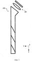
- FIG. 10 is a drawing illustrating the general configuration and optical path in the XY plane of a photoreceptor device of the present invention. Similar parts have been assigned the same reference symbols as in goggle type display 101 described above.
- the photoreceptor device 401 comprises a photoreceptor unit (photoreceptor optical system) 440 which receives light, and a light guide unit (optical element) 100 which internally reflects light from the outside, guiding it to the photoreceptor unit 440.
- a photoreceptor unit photoreceptor optical system
- a light guide unit optical element
- the photoreceptor unit 440 comprises a photoreceptor mechanism arranged opposite the right surface 10c and having a photoreceptor element 441 and optical system 42; and a control unit (not illustrated) in which signals from the photoreceptor mechanism are inputted.
- first main beam splitter surface 11a first main beam splitter surface 11a, second main beam splitter surface 11b and third main beam splitter surface 11c.
- first main beam splitter surface 11a, the second main beam splitter surface 11b and the third main beam splitter surface 11c reflect a prescribed fraction of the luminous flux of the inputted light so that it advances substantially in the -X direction, and transmit a prescribed fraction of the luminous flux of the light.
- the front surface 10a and rear surface 10b reflect the light multiple times in alternation, causing it to advance in the -X direction (set direction).
- the advancing light reaches the secondary beam splitter surface 30 (front surface 10a), and the secondary beam splitter surface 30 (front surface 10a) reflects a set fraction of the luminous flux of the inputted light and transmits a set fraction of the luminous flux of the light.
- the secondary beam splitter surface 30 front surface 10a
- a set fraction of the luminous flux of the light advances through the inside of the main substrate 10
- a set fraction of the luminous flux of the light advances inside the secondary substrate 20.
- the light which has advanced inside the secondary substrate 20 is reflected by the front surface 20a and then reaches the secondary beam splitter surface 30 (front surface 10a).
- the secondary beam splitter surface 30 (front surface 10a) reflects a set fraction of the luminous flux of the inputted light and transmits a set fraction of the luminous flux of the light. Namely, a set fraction of the luminous flux of the light advances inside the main substrate 10 and a set fraction of the luminous flux of the light advances through the inside of the secondary substrate 20.
- the photoreceptor device 401 of the present invention As described above, the total luminous flux which reaches the first main beam splitter surface 11a, second main beam splitter surface 11b and third main beam splitter surface 11c can be received.
- the photoreceptor device 401 of the present invention is able to sense the object of sensing in whatever region of the luminous flux is may be present.
- the present invention can be used in optical elements, etc. for propagating light in a set direction.
Landscapes
- Physics & Mathematics (AREA)
- General Physics & Mathematics (AREA)
- Optics & Photonics (AREA)
- Health & Medical Sciences (AREA)
- Ophthalmology & Optometry (AREA)
- General Health & Medical Sciences (AREA)
- Engineering & Computer Science (AREA)
- Multimedia (AREA)
- Signal Processing (AREA)
- Optical Elements Other Than Lenses (AREA)
Applications Claiming Priority (1)
| Application Number | Priority Date | Filing Date | Title |
|---|---|---|---|
| PCT/JP2016/051210 WO2017125992A1 (fr) | 2016-01-18 | 2016-01-18 | Elément optique, dispositif d'affichage utilisant celui-ci, et dispositif de réception de lumière |
Publications (3)
| Publication Number | Publication Date |
|---|---|
| EP3407116A1 true EP3407116A1 (fr) | 2018-11-28 |
| EP3407116A4 EP3407116A4 (fr) | 2019-09-25 |
| EP3407116B1 EP3407116B1 (fr) | 2025-06-25 |
Family
ID=59361781
Family Applications (1)
| Application Number | Title | Priority Date | Filing Date |
|---|---|---|---|
| EP16886235.7A Active EP3407116B1 (fr) | 2016-01-18 | 2016-01-18 | Élément optique, dispositif d'affichage utilisant celui-ci et dispositif photorécepteur |
Country Status (5)
| Country | Link |
|---|---|
| US (1) | US11262564B2 (fr) |
| EP (1) | EP3407116B1 (fr) |
| JP (1) | JP6562088B2 (fr) |
| TW (1) | TWI631368B (fr) |
| WO (1) | WO2017125992A1 (fr) |
Families Citing this family (19)
| Publication number | Priority date | Publication date | Assignee | Title |
|---|---|---|---|---|
| IL237337B (en) * | 2015-02-19 | 2020-03-31 | Amitai Yaakov | A compact head-up display system with a uniform image |
| JP6980209B2 (ja) | 2017-02-22 | 2021-12-15 | ルムス エルティーディー. | 光ガイド光学アセンブリ |
| JP7064581B2 (ja) | 2017-09-28 | 2022-05-10 | マジック リープ, インコーポレイテッド | 光学結像システムの接眼レンズからの迷光放出を低減させる方法および装置 |
| US11415812B2 (en) | 2018-06-26 | 2022-08-16 | Lumus Ltd. | Compact collimating optical device and system |
| US11698532B2 (en) * | 2018-07-10 | 2023-07-11 | Shimadzu Corporation | Image display device |
| TWI827663B (zh) | 2018-09-06 | 2024-01-01 | 以色列商魯姆斯有限公司 | 具有雷射二極體照明的近眼顯示器 |
| WO2020183229A1 (fr) | 2019-03-12 | 2020-09-17 | Lumus Ltd. | Projecteur d'image |
| IL289182B2 (en) | 2019-07-04 | 2024-06-01 | Lumus Ltd | Figure waveguide with symmetric light beam multiplication |
| KR102893003B1 (ko) | 2019-09-16 | 2025-11-27 | 루머스 리미티드 | 헤드 마운트 디스플레이용 컴팩트 프로젝터 |
| CN114207354B (zh) * | 2019-09-16 | 2024-06-21 | 鲁姆斯有限公司 | 具有光束倍增的图像显示系统 |
| KR102939032B1 (ko) | 2019-12-05 | 2026-03-16 | 루머스 리미티드 | 상보 코팅된 부분적 반사체를 채용하는 도광 광학 소자, 및 광산란을 감소시킨 도광 광학 소자 |
| WO2021148892A1 (fr) | 2020-01-20 | 2021-07-29 | Ricoh Company, Ltd. | Guide de lumière et dispositif d'affichage d'image virtuelle |
| JP2021149008A (ja) * | 2020-03-19 | 2021-09-27 | 株式会社リコー | 導光体および虚像表示装置 |
| JP7380240B2 (ja) * | 2020-01-20 | 2023-11-15 | 株式会社リコー | 導光部材および虚像表示装置 |
| US12164136B2 (en) * | 2020-02-07 | 2024-12-10 | Shimadzu Corporation | Display device and optical element for use in the display device |
| CN115176190B (zh) | 2020-05-24 | 2024-07-09 | 鲁姆斯有限公司 | 复合光导光学元件 |
| CN114114518A (zh) * | 2020-08-28 | 2022-03-01 | 中强光电股份有限公司 | 光波导、光波导的制作方法以及头戴式显示装置 |
| JP2024532842A (ja) | 2021-08-23 | 2024-09-10 | ルーマス リミテッド | 埋め込まれた結合反射器を有する複合導光光学素子の作製方法 |
| KR20250053044A (ko) | 2022-08-18 | 2025-04-21 | 루머스 리미티드 | 편광 반사굴절 시준기를 갖는 이미지 프로젝터 |
Family Cites Families (14)
| Publication number | Priority date | Publication date | Assignee | Title |
|---|---|---|---|---|
| JP4727034B2 (ja) * | 2000-11-28 | 2011-07-20 | オリンパス株式会社 | 観察光学系および撮像光学系 |
| EP1748305A4 (fr) * | 2004-05-17 | 2009-01-14 | Nikon Corp | Élément optique, système optique combinateur et unite d'affichage d'image |
| IL173715A0 (en) * | 2006-02-14 | 2007-03-08 | Lumus Ltd | Substrate-guided imaging lens |
| US7589901B2 (en) * | 2007-07-10 | 2009-09-15 | Microvision, Inc. | Substrate-guided relays for use with scanned beam light sources |
| WO2011024291A1 (fr) | 2009-08-28 | 2011-03-03 | 株式会社島津製作所 | Dispositif d'affichage |
| JP5240214B2 (ja) | 2010-02-15 | 2013-07-17 | 株式会社島津製作所 | 表示装置 |
| JP2011186332A (ja) * | 2010-03-10 | 2011-09-22 | Shimadzu Corp | 表示装置 |
| JP5471986B2 (ja) * | 2010-09-07 | 2014-04-16 | 株式会社島津製作所 | 光学部品及びそれを用いた表示装置 |
| JP5901192B2 (ja) * | 2011-09-13 | 2016-04-06 | オリンパス株式会社 | 光学機構 |
| US20130108229A1 (en) * | 2011-10-28 | 2013-05-02 | Google Inc. | Heads-up display including ambient light control |
| US9519092B1 (en) * | 2012-03-21 | 2016-12-13 | Google Inc. | Display method |
| JP6225657B2 (ja) * | 2013-11-15 | 2017-11-08 | セイコーエプソン株式会社 | 光学素子および画像表示装置並びにこれらの製造方法 |
| IL237337B (en) * | 2015-02-19 | 2020-03-31 | Amitai Yaakov | A compact head-up display system with a uniform image |
| WO2017038350A1 (fr) * | 2015-09-02 | 2017-03-09 | ソニー株式会社 | Dispositif optique et son procédé de production, et dispositif d'affichage |
-
2016
- 2016-01-18 US US15/767,000 patent/US11262564B2/en active Active
- 2016-01-18 WO PCT/JP2016/051210 patent/WO2017125992A1/fr not_active Ceased
- 2016-01-18 JP JP2017562168A patent/JP6562088B2/ja active Active
- 2016-01-18 EP EP16886235.7A patent/EP3407116B1/fr active Active
-
2017
- 2017-01-06 TW TW106100380A patent/TWI631368B/zh not_active IP Right Cessation
Also Published As
| Publication number | Publication date |
|---|---|
| JP6562088B2 (ja) | 2019-08-21 |
| US11262564B2 (en) | 2022-03-01 |
| TWI631368B (zh) | 2018-08-01 |
| US20180307014A1 (en) | 2018-10-25 |
| EP3407116A4 (fr) | 2019-09-25 |
| EP3407116B1 (fr) | 2025-06-25 |
| JPWO2017125992A1 (ja) | 2018-05-31 |
| WO2017125992A1 (fr) | 2017-07-27 |
| TW201743103A (zh) | 2017-12-16 |
Similar Documents
| Publication | Publication Date | Title |
|---|---|---|
| EP3407116B1 (fr) | Élément optique, dispositif d'affichage utilisant celui-ci et dispositif photorécepteur | |
| US9465215B2 (en) | Lightguide with multiple in-coupling holograms for head wearable display | |
| US20210157150A1 (en) | Compact head-mounted display system | |
| US9612448B2 (en) | Display device and wearable glasses | |
| JP2022553595A (ja) | 高屈折率部分を伴うディスプレイ導波路 | |
| JP2018060178A (ja) | ヘッドマウントディスプレイ装置及び光学系 | |
| JP2012058404A (ja) | 光学部品及びそれを用いた表示装置 | |
| JP5152101B2 (ja) | 表示装置 | |
| US20230107434A1 (en) | Geometrical waveguide illuminator and display based thereon | |
| KR102072012B1 (ko) | 헤드마운트 디스플레이장치 | |
| WO2022120253A1 (fr) | Dispositif d'affichage avec illuminateur transparent | |
| JP2019113721A (ja) | 導光装置及び表示装置 | |
| US20220179211A1 (en) | Display device with transparent illuminator | |
| EP3805840A1 (fr) | Dispositif d'affichage d'image | |
| JP2011186332A (ja) | 表示装置 | |
| US11774753B1 (en) | Cascaded pupil-replicating waveguides | |
| EP4399560A1 (fr) | Guide de lumière à réplication de pupille radiale et affichage visuel basé sur celui-ci | |
| CN112748492A (zh) | 导光装置、显示装置和导光装置的制造方法 | |
| KR101815732B1 (ko) | 애너모픽 렌즈를 이용한 광학 장치 | |
| WO2023097806A1 (fr) | Module optique et dispositif électronique | |
| TW202307516A (zh) | 多源光導照明器 | |
| JP5861332B2 (ja) | 表示装置 | |
| EP3805846A1 (fr) | Dispositif d'affichage d'image | |
| KR102072008B1 (ko) | 헤드마운트 디스플레이장치 | |
| CN119137528A (zh) | 通过图像光重定向的视场扩展 |
Legal Events
| Date | Code | Title | Description |
|---|---|---|---|
| STAA | Information on the status of an ep patent application or granted ep patent |
Free format text: STATUS: THE INTERNATIONAL PUBLICATION HAS BEEN MADE |
|
| PUAI | Public reference made under article 153(3) epc to a published international application that has entered the european phase |
Free format text: ORIGINAL CODE: 0009012 |
|
| STAA | Information on the status of an ep patent application or granted ep patent |
Free format text: STATUS: REQUEST FOR EXAMINATION WAS MADE |
|
| 17P | Request for examination filed |
Effective date: 20180813 |
|
| AK | Designated contracting states |
Kind code of ref document: A1 Designated state(s): AL AT BE BG CH CY CZ DE DK EE ES FI FR GB GR HR HU IE IS IT LI LT LU LV MC MK MT NL NO PL PT RO RS SE SI SK SM TR |
|
| AX | Request for extension of the european patent |
Extension state: BA ME |
|
| DAV | Request for validation of the european patent (deleted) | ||
| DAX | Request for extension of the european patent (deleted) | ||
| A4 | Supplementary search report drawn up and despatched |
Effective date: 20190823 |
|
| RIC1 | Information provided on ipc code assigned before grant |
Ipc: H04N 5/64 20060101ALI20190819BHEP Ipc: G02B 27/02 20060101AFI20190819BHEP Ipc: G02B 17/08 20060101ALI20190819BHEP Ipc: G02C 7/00 20060101ALI20190819BHEP |
|
| STAA | Information on the status of an ep patent application or granted ep patent |
Free format text: STATUS: EXAMINATION IS IN PROGRESS |
|
| 17Q | First examination report despatched |
Effective date: 20221207 |
|
| REG | Reference to a national code |
Ref country code: DE Ref legal event code: R079 Free format text: PREVIOUS MAIN CLASS: G02B0027020000 Ipc: G02B0027000000 Ref country code: DE Ref legal event code: R079 Ref document number: 602016092694 Country of ref document: DE Free format text: PREVIOUS MAIN CLASS: G02B0027020000 Ipc: G02B0027000000 |
|
| GRAP | Despatch of communication of intention to grant a patent |
Free format text: ORIGINAL CODE: EPIDOSNIGR1 |
|
| STAA | Information on the status of an ep patent application or granted ep patent |
Free format text: STATUS: GRANT OF PATENT IS INTENDED |
|
| RIC1 | Information provided on ipc code assigned before grant |
Ipc: G02B 6/00 20060101ALI20250206BHEP Ipc: G02B 27/01 20060101ALI20250206BHEP Ipc: G02C 7/08 20060101ALI20250206BHEP Ipc: G02B 27/00 20060101AFI20250206BHEP |
|
| INTG | Intention to grant announced |
Effective date: 20250228 |
|
| GRAS | Grant fee paid |
Free format text: ORIGINAL CODE: EPIDOSNIGR3 |
|
| GRAA | (expected) grant |
Free format text: ORIGINAL CODE: 0009210 |
|
| STAA | Information on the status of an ep patent application or granted ep patent |
Free format text: STATUS: THE PATENT HAS BEEN GRANTED |
|
| AK | Designated contracting states |
Kind code of ref document: B1 Designated state(s): AL AT BE BG CH CY CZ DE DK EE ES FI FR GB GR HR HU IE IS IT LI LT LU LV MC MK MT NL NO PL PT RO RS SE SI SK SM TR |
|
| REG | Reference to a national code |
Ref country code: GB Ref legal event code: FG4D |
|
| REG | Reference to a national code |
Ref country code: CH Ref legal event code: EP |
|
| REG | Reference to a national code |
Ref country code: CH Ref legal event code: EP |
|
| REG | Reference to a national code |
Ref country code: IE Ref legal event code: FG4D |
|
| REG | Reference to a national code |
Ref country code: DE Ref legal event code: R096 Ref document number: 602016092694 Country of ref document: DE |
|
| PG25 | Lapsed in a contracting state [announced via postgrant information from national office to epo] |
Ref country code: FI Free format text: LAPSE BECAUSE OF FAILURE TO SUBMIT A TRANSLATION OF THE DESCRIPTION OR TO PAY THE FEE WITHIN THE PRESCRIBED TIME-LIMIT Effective date: 20250625 |
|
| REG | Reference to a national code |
Ref country code: LT Ref legal event code: MG9D |
|
| PG25 | Lapsed in a contracting state [announced via postgrant information from national office to epo] |
Ref country code: GR Free format text: LAPSE BECAUSE OF FAILURE TO SUBMIT A TRANSLATION OF THE DESCRIPTION OR TO PAY THE FEE WITHIN THE PRESCRIBED TIME-LIMIT Effective date: 20250926 Ref country code: NO Free format text: LAPSE BECAUSE OF FAILURE TO SUBMIT A TRANSLATION OF THE DESCRIPTION OR TO PAY THE FEE WITHIN THE PRESCRIBED TIME-LIMIT Effective date: 20250925 |
|
| PG25 | Lapsed in a contracting state [announced via postgrant information from national office to epo] |
Ref country code: BG Free format text: LAPSE BECAUSE OF FAILURE TO SUBMIT A TRANSLATION OF THE DESCRIPTION OR TO PAY THE FEE WITHIN THE PRESCRIBED TIME-LIMIT Effective date: 20250625 |
|
| PG25 | Lapsed in a contracting state [announced via postgrant information from national office to epo] |
Ref country code: HR Free format text: LAPSE BECAUSE OF FAILURE TO SUBMIT A TRANSLATION OF THE DESCRIPTION OR TO PAY THE FEE WITHIN THE PRESCRIBED TIME-LIMIT Effective date: 20250625 |
|
| PG25 | Lapsed in a contracting state [announced via postgrant information from national office to epo] |
Ref country code: RS Free format text: LAPSE BECAUSE OF FAILURE TO SUBMIT A TRANSLATION OF THE DESCRIPTION OR TO PAY THE FEE WITHIN THE PRESCRIBED TIME-LIMIT Effective date: 20250925 |
|
| PG25 | Lapsed in a contracting state [announced via postgrant information from national office to epo] |
Ref country code: LV Free format text: LAPSE BECAUSE OF FAILURE TO SUBMIT A TRANSLATION OF THE DESCRIPTION OR TO PAY THE FEE WITHIN THE PRESCRIBED TIME-LIMIT Effective date: 20250625 |
|
| REG | Reference to a national code |
Ref country code: NL Ref legal event code: MP Effective date: 20250625 |
|
| PG25 | Lapsed in a contracting state [announced via postgrant information from national office to epo] |
Ref country code: NL Free format text: LAPSE BECAUSE OF FAILURE TO SUBMIT A TRANSLATION OF THE DESCRIPTION OR TO PAY THE FEE WITHIN THE PRESCRIBED TIME-LIMIT Effective date: 20250625 |
|
| PG25 | Lapsed in a contracting state [announced via postgrant information from national office to epo] |
Ref country code: PT Free format text: LAPSE BECAUSE OF FAILURE TO SUBMIT A TRANSLATION OF THE DESCRIPTION OR TO PAY THE FEE WITHIN THE PRESCRIBED TIME-LIMIT Effective date: 20251027 |
|
| REG | Reference to a national code |
Ref country code: AT Ref legal event code: MK05 Ref document number: 1807058 Country of ref document: AT Kind code of ref document: T Effective date: 20250625 |
|
| PG25 | Lapsed in a contracting state [announced via postgrant information from national office to epo] |
Ref country code: IS Free format text: LAPSE BECAUSE OF FAILURE TO SUBMIT A TRANSLATION OF THE DESCRIPTION OR TO PAY THE FEE WITHIN THE PRESCRIBED TIME-LIMIT Effective date: 20251025 |
|
| PGFP | Annual fee paid to national office [announced via postgrant information from national office to epo] |
Ref country code: GB Payment date: 20251127 Year of fee payment: 11 |
|
| PG25 | Lapsed in a contracting state [announced via postgrant information from national office to epo] |
Ref country code: SM Free format text: LAPSE BECAUSE OF FAILURE TO SUBMIT A TRANSLATION OF THE DESCRIPTION OR TO PAY THE FEE WITHIN THE PRESCRIBED TIME-LIMIT Effective date: 20250625 Ref country code: AT Free format text: LAPSE BECAUSE OF FAILURE TO SUBMIT A TRANSLATION OF THE DESCRIPTION OR TO PAY THE FEE WITHIN THE PRESCRIBED TIME-LIMIT Effective date: 20250625 |
|
| PGFP | Annual fee paid to national office [announced via postgrant information from national office to epo] |
Ref country code: FR Payment date: 20251128 Year of fee payment: 11 |
|
| PG25 | Lapsed in a contracting state [announced via postgrant information from national office to epo] |
Ref country code: CZ Free format text: LAPSE BECAUSE OF FAILURE TO SUBMIT A TRANSLATION OF THE DESCRIPTION OR TO PAY THE FEE WITHIN THE PRESCRIBED TIME-LIMIT Effective date: 20250625 |
|
| PG25 | Lapsed in a contracting state [announced via postgrant information from national office to epo] |
Ref country code: PL Free format text: LAPSE BECAUSE OF FAILURE TO SUBMIT A TRANSLATION OF THE DESCRIPTION OR TO PAY THE FEE WITHIN THE PRESCRIBED TIME-LIMIT Effective date: 20250625 |
|
| PG25 | Lapsed in a contracting state [announced via postgrant information from national office to epo] |
Ref country code: EE Free format text: LAPSE BECAUSE OF FAILURE TO SUBMIT A TRANSLATION OF THE DESCRIPTION OR TO PAY THE FEE WITHIN THE PRESCRIBED TIME-LIMIT Effective date: 20250625 |
|
| PG25 | Lapsed in a contracting state [announced via postgrant information from national office to epo] |
Ref country code: RO Free format text: LAPSE BECAUSE OF FAILURE TO SUBMIT A TRANSLATION OF THE DESCRIPTION OR TO PAY THE FEE WITHIN THE PRESCRIBED TIME-LIMIT Effective date: 20250625 Ref country code: SK Free format text: LAPSE BECAUSE OF FAILURE TO SUBMIT A TRANSLATION OF THE DESCRIPTION OR TO PAY THE FEE WITHIN THE PRESCRIBED TIME-LIMIT Effective date: 20250625 |
|
| PG25 | Lapsed in a contracting state [announced via postgrant information from national office to epo] |
Ref country code: ES Free format text: LAPSE BECAUSE OF FAILURE TO SUBMIT A TRANSLATION OF THE DESCRIPTION OR TO PAY THE FEE WITHIN THE PRESCRIBED TIME-LIMIT Effective date: 20250625 |
|
| PG25 | Lapsed in a contracting state [announced via postgrant information from national office to epo] |
Ref country code: DK Free format text: LAPSE BECAUSE OF FAILURE TO SUBMIT A TRANSLATION OF THE DESCRIPTION OR TO PAY THE FEE WITHIN THE PRESCRIBED TIME-LIMIT Effective date: 20250625 |
|
| PGFP | Annual fee paid to national office [announced via postgrant information from national office to epo] |
Ref country code: DE Payment date: 20251203 Year of fee payment: 11 |
|
| PGFP | Annual fee paid to national office [announced via postgrant information from national office to epo] |
Ref country code: IT Payment date: 20251219 Year of fee payment: 11 |
|
| PLBE | No opposition filed within time limit |
Free format text: ORIGINAL CODE: 0009261 |
|
| STAA | Information on the status of an ep patent application or granted ep patent |
Free format text: STATUS: NO OPPOSITION FILED WITHIN TIME LIMIT |