EP3407182A1 - Dispositif informatique de calcul de vecteur - Google Patents
Dispositif informatique de calcul de vecteur Download PDFInfo
- Publication number
- EP3407182A1 EP3407182A1 EP16885912.2A EP16885912A EP3407182A1 EP 3407182 A1 EP3407182 A1 EP 3407182A1 EP 16885912 A EP16885912 A EP 16885912A EP 3407182 A1 EP3407182 A1 EP 3407182A1
- Authority
- EP
- European Patent Office
- Prior art keywords
- vector
- instruction
- unit
- operation instruction
- operations
- Prior art date
- Legal status (The legal status is an assumption and is not a legal conclusion. Google has not performed a legal analysis and makes no representation as to the accuracy of the status listed.)
- Granted
Links
Images

Classifications
-
- G—PHYSICS
- G06—COMPUTING OR CALCULATING; COUNTING
- G06F—ELECTRIC DIGITAL DATA PROCESSING
- G06F9/00—Arrangements for program control, e.g. control units
- G06F9/06—Arrangements for program control, e.g. control units using stored programs, i.e. using an internal store of processing equipment to receive or retain programs
- G06F9/30—Arrangements for executing machine instructions, e.g. instruction decode
- G06F9/30003—Arrangements for executing specific machine instructions
- G06F9/30007—Arrangements for executing specific machine instructions to perform operations on data operands
- G06F9/30036—Instructions to perform operations on packed data, e.g. vector, tile or matrix operations
-
- G—PHYSICS
- G06—COMPUTING OR CALCULATING; COUNTING
- G06F—ELECTRIC DIGITAL DATA PROCESSING
- G06F17/00—Digital computing or data processing equipment or methods, specially adapted for specific functions
- G06F17/10—Complex mathematical operations
- G06F17/16—Matrix or vector computation, e.g. matrix-matrix or matrix-vector multiplication, matrix factorization
-
- G—PHYSICS
- G06—COMPUTING OR CALCULATING; COUNTING
- G06F—ELECTRIC DIGITAL DATA PROCESSING
- G06F9/00—Arrangements for program control, e.g. control units
- G06F9/06—Arrangements for program control, e.g. control units using stored programs, i.e. using an internal store of processing equipment to receive or retain programs
- G06F9/30—Arrangements for executing machine instructions, e.g. instruction decode
- G06F9/30003—Arrangements for executing specific machine instructions
- G06F9/30007—Arrangements for executing specific machine instructions to perform operations on data operands
- G06F9/3001—Arithmetic instructions
-
- G—PHYSICS
- G06—COMPUTING OR CALCULATING; COUNTING
- G06F—ELECTRIC DIGITAL DATA PROCESSING
- G06F9/00—Arrangements for program control, e.g. control units
- G06F9/06—Arrangements for program control, e.g. control units using stored programs, i.e. using an internal store of processing equipment to receive or retain programs
- G06F9/30—Arrangements for executing machine instructions, e.g. instruction decode
- G06F9/30098—Register arrangements
- G06F9/3012—Organisation of register space, e.g. banked or distributed register file
- G06F9/3013—Organisation of register space, e.g. banked or distributed register file according to data content, e.g. floating-point registers, address registers
-
- G—PHYSICS
- G06—COMPUTING OR CALCULATING; COUNTING
- G06F—ELECTRIC DIGITAL DATA PROCESSING
- G06F9/00—Arrangements for program control, e.g. control units
- G06F9/06—Arrangements for program control, e.g. control units using stored programs, i.e. using an internal store of processing equipment to receive or retain programs
- G06F9/30—Arrangements for executing machine instructions, e.g. instruction decode
- G06F9/34—Addressing or accessing the instruction operand or the result ; Formation of operand address; Addressing modes
- G06F9/35—Indirect addressing
-
- G—PHYSICS
- G06—COMPUTING OR CALCULATING; COUNTING
- G06F—ELECTRIC DIGITAL DATA PROCESSING
- G06F9/00—Arrangements for program control, e.g. control units
- G06F9/06—Arrangements for program control, e.g. control units using stored programs, i.e. using an internal store of processing equipment to receive or retain programs
- G06F9/30—Arrangements for executing machine instructions, e.g. instruction decode
- G06F9/38—Concurrent instruction execution, e.g. pipeline or look ahead
- G06F9/3824—Operand accessing
Definitions
- the subject disclosure relates to a vector computing device for executing vector operations according to a vector operation instruction, offering a solution to the problem in the prior art where more and more algorithms involve a large number of vector operations.
- one solution to conduct vector operation is to use a general-purpose processor by executing a general instruction via general-purpose register file and general-purpose functional unit to perform vector operations.
- one defect of the solution is the low operation performance during vector operation triggered because a single general-purpose processor is primarily used for scalar computation.
- using multiple general-purpose processors for concurrent execution may lead to a possible performance bottleneck resulting from the intercommunication among such processors.
- GPU graphics processing unit
- general-purpose register file and general-purpose stream processing unit are used to execute general SIMD instruction, thereby performing vector operation.
- general-purpose register file and general-purpose stream processing unit are used to execute general SIMD instruction, thereby performing vector operation.
- general-purpose register file and general-purpose stream processing unit are used to execute general SIMD instruction, thereby performing vector operation.
- a specialized vector operation device is used to perform vector computation, wherein customized register file and processing unit are used to perform vector operation. Limited by the register file, however, the present specialized vector operation device is unable to flexibly support vector operations of different lengths.
- the subject disclosure aims to provide a vector computing device to solve the problems existing in the prior art, such as inter-chip communication, insufficient on-chip cache, and inflexible supported vector length.
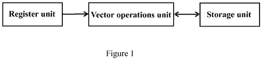
- the subject disclosure provides a vector computing device used for executing a vector operation according to a vector operation instruction, comprising:
- a storage unit for storing vectors.
- a register unit for storing vector addresses, wherein vector addresses are the addresses where vectors are stored in the storage unit.
- a vector operations unit for acquiring a vector operation instruction, obtaining a vector address from the register unit according to the vector operation instruction, and then gaining a corresponding vector from the storage unit according to the vector address, subsequently performing a vector operation according to the acquired vector so as to have a vector operation result.
- the vector computing device in the subject disclosure is able to temporarily store vector data involved in computation in a Scratchpad Memory, allowing vector operation to support widths with different data more flexibly and effectively while enabling an improved performance for executing computing tasks comprising a large number of vectors.
- a vector computing device of the present disclosure comprises a storage unit, a register unit and a vector operations unit, wherein vectors are stored in the storage unit, vector storage addresses are stored in the register unit, and the vector operations unit acquires a vector address from the register unit according to a vector operation instruction, and then acquires a corresponding vector from the storage unit according to the vector address, subsequently perform a vector operation according to the acquired vector so as to obtain a vector operation result.
- the vector computing device in the subject disclosure is able to temporarily store vector data involved in computation in a Scratchpad Memory, allowing in the process of vector operation to support data with different widths more flexibly and effectively while enabling an improved performance for executing computing tasks comprising a large number of vectors.
- Fig. 1 is a structure diagram of the vector computing device provided by the subject disclosure. As shown in Fig. 1 , the vector computing device comprises:
- the storage unit can be a Scratchpad Memory for supporting vector data of different sizes; in the subject disclosure, the necessary computational data are temporarily stored in the Scratchpad Memory to enable the computing device to more flexibly and effectively support data of different widths during vector operations.
- the register unit for storing vector addresses, wherein vector addresses are the ones where the vectors are stored in the storage unit;
- the register unit can be a scalar register file providing a scalar register as required during operations, and the scalar register stores vector addresses as well as scalar data.
- the vector operations unit is not only to acquire a vector address from the register unit, but also to obtain a corresponding scalar from the register unit.
- a vector operations unit for acquiring a vector operation instruction, obtaining a vector address from said register unit according to the vector operation instruction, and then gaining a corresponding vector from the storage unit according to the vector address, subsequently performing a vector operation according to the acquired vector so as to obtain a vector operation result and store the vector operation result in the storage unit.
- the vector operations unit comprises a vector addition element, a vector multiplication element, a value comparing element, a nonlinear operation element and a vector-scalar-multiplication element; furthermore, the vector operations unit is of the structure of multiple-stage pipeline, wherein the vector addition element and the vector multiplication element are arranged in the first stage of pipeline, the value comparing element in the second stage, and the nonlinear operation element and the vector-scalar-multiplication element in the third stage. Due to the fact that such elements are arranged in different stages of pipeline, when the order of the successive serial multiple vector operation instructions is consistent with pipeline order of the corresponding units, the operations as demanded by the series of vector operation instructions can be more effectively achieved.
- All the vector operations of the device are performed by the vector operations unit, including but not limited to vector addition operation, vector added to scalar operation, vector subtraction operation, scalar subtracted from vector operation, vector multiplication operation, vector multiplied by scalar operation, vector division (contrapuntally divided) operation, vector AND operation, and vector OR operation, and the vector operation instructions are sent to the operations unit for execution.
- the vector computing device further comprises an instruction cache unit for storing a vector operation instruction to be executed. While being executed, an instruction is cached in the instruction cache unit as well. When execution of an instruction has been completed, if such instruction is also the earliest one among those instructions in the instruction cache unit that have not been submitted, then it will be submitted; once such instruction is submitted, the status change of the device caused by operation performed by such instruction cannot be cancelled.
- the instruction cache unit can be a reorder cache.
- the vector computing device further comprises an instruction processing unit for acquiring a vector operation instruction from the instruction cache unit and processing the vector operation instruction and providing it to said vector operations unit, wherein the instruction processing unit comprises:
- an instruction fetching module for acquiring a vector operation instruction from the instruction cache unit
- a decoding module for decoding the acquired vector operation instruction
- the vector computing device further comprises a dependency relationship processing unit for: before the vector operations unit acquires the vector operation instruction, determining whether the vector operation instruction accesses the same vector as the previous vector operation instruction: if it does, the vector operation instruction will be stored in a storage queue, and that vector operation instruction in the storage queue will then be provided to said vector operations unit until the execution of the previous vector operation instruction is completed; otherwise, the vector operation instruction will be directly provided to said vector operations unit.
- a dependency relationship processing unit for: before the vector operations unit acquires the vector operation instruction, determining whether the vector operation instruction accesses the same vector as the previous vector operation instruction: if it does, the vector operation instruction will be stored in a storage queue, and that vector operation instruction in the storage queue will then be provided to said vector operations unit until the execution of the previous vector operation instruction is completed; otherwise, the vector operation instruction will be directly provided to said vector operations unit.
- successive instructions may access the same memory space, and to ensure the correctness of an execution result of the instruction, the present instruction, if detected to have a dependency relationship with data of the previous instruction, must wait within the storage queue until such dependency relationship is eliminated.
- the vector computing device further comprises an in-out unit for storing vectors in the storage unit, or for acquiring a vector operation result from the storage unit, wherein the in-out unit can directly connect with the storage unit and is used for reading or writing vector data from or in the memory.
- structure of Load/Store is adopted by the instruction set used for the device of the subject disclosure, and the vector operations unit will not operate data in the memory.
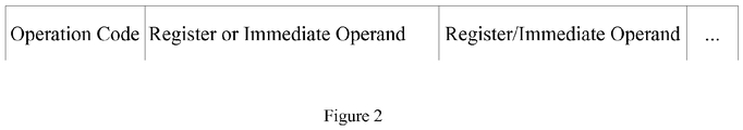
- the instruction set adopts fixed length instruction.
- Fig.2 is a format diagram of the instruction set provided by the subject disclosure.
- the vector operation instruction includes an operation code and at least one operation field, wherein the operation code is used for indicating function of the vector operation instruction, and the vector operations unit is to perform different vector operations by identifying the operation code; and the operation field is used for indicating data information of the vector operation instruction, wherein data information can be an immediate operand or a register number.
- data information can be an immediate operand or a register number.
- the instruction set comprises vector operation instructions different in function.
- VA Vector Addition Instruction
- the device respectively retrieves two blocks of vector data of a specified size from specified addresses of the Scratchpad Memory to performs addition operation in the vector operations unit, and writes the result back into a specified address of the Scratchpad Memory;
- VAS Vector Added to Scalar Instruction
- the device retrieves vector data of a specified size from a specified address of the Scratchpad Memory and scalar data from a specified address of the scalar register file, adds the scalar value to each element of vector in the scalar operations unit, and writes the result back into a specified address of the Scratchpad Memory;
- the device respectively retrieves two blocks of vector data of a specified size from specified addresses of the Scratchpad Memory, performs subtraction operation in the vector operations unit, and writes the result back into a specified address of the Scratchpad Memory;
- Scalar Subtracted Vector Instruction According the instruction, the device retrieves scalar data from a specified address of the scalar register file and vector data from a specified address of the Scratchpad Memory , subtracts the corresponding element of the vector from the scalar in the vector operations unit, and writes the result back into a specified address of the Scratchpad Memory;
- VMV Vector Multiplied by Vector Instruction
- VMS Vector Multiplied by Scalar Instruction
- the device retrieves vector data of a specified size from a specified address of the Scratchpad Memory and scalar data of a specified size from a specified address of the scalar register file, performs a Vector Multiplied by Scalar operation in the vector register unit, and writes the result back into a specified address of the Scratchpad Memory;
- VD Vector Division Instruction
- the device respectively retrieves vector data of a specified size from specified addresses of the Scratchpad Memory, contrapuntally divides two vectors in the vector operations unit, and writes the result back into a specified address of the Scratchpad Memory;
- the device retrieves scalar data from a specified address of the scalar register file and vector data of a specified size from a specified address of the Scratchpad Memory, respectively divides the scalar by the respective element of the vector in the vector operations unit, and writes the result back into a specified address of the Scratchpad Memory;
- VAV Vector AND Vector Instruction
- VAND Vector AND Instruction
- the device retrieves vector data of a specified size from a specified address of the Scratchpad Memory, performs AND operations on each bit of the vector in the vector operations unit, and writes the result back into a specified address of the scalar register file;
- VOV Vector OR Vector Instruction
- VOR Vector OR Instruction
- the device retrieves vector data of a specified size from a specified address of the Scratchpad Memory, performs OR operations on each bit of the vectors in the vector operations unit, and writes the result back into a specified address of the scalar register file;
- the device retrieves vector data of a specified size from a specified address of the Scratchpad Memory, performs exponent operation for each element of the vector in the vector operations unit, and writes the result back into a specified address of the Scratchpad Memory;
- VL Vector Logarithm Instruction
- the device retrieves vector data of a specified size from a specified address of the Scratchpad Memory, performs logarithm operation for each element of the vector in the vector operations unit, and writes the result back into a specified address of the Scratchpad Memory;
- VCT Vector Greater than Instruction
- the device respectively retrieves vector data of a specified size from specified addresses of the Scratchpad Memory, contrapuntally compares two vector data in the vector operations unit, then places "1" in the respective position in an output vector if the former one is greater than the latter, while places "0” otherwise, and writes the result back into a specified address of the Scratchpad Memory;
- VEQ Vector Equal Decision Instruction
- VNV Vector Inverter Instruction
- VMER Vector Merger Instruction
- the device respectively retrieves vector data of a specified size from specified addresses of the Scratchpad Memory, including a selecting vector and a selected vector I and a selected vector II. According to whether an element of the selecting vector is "1" or "0", the vector operations unit selects from the selected vector I or the selected vector II a corresponding element as an element in a corresponding position in an output vector, and writes the result back into a specified address of the Scratchpad Memory;
- VMAX Vector Maximum Instruction
- Scalar to Vector Instruction According to the instruction, the device retrieves scalar data from a specified address of the scalar register file, extends the scalar to be a vector of a specified length in the vector operations unit, and writes the result back into the scalar register file;
- Scalar to Vector Pos N Instruction STVPN.
- the device retrieves scalar from a specified address of the scalar register file and vector data of a specified size from a specified address of the Scratchpad Memory, replaces an element in a specified position of the vector with the scalar value in the vector operations unit, and writes the result back into a specified address of the Scratchpad Memory;
- the device retrieves scalar from a specified address of the scalar register file and vector data of a specified size from a specified address of the Scratchpad Memory, replaces the scalar value with an element in a specified position of the vector in the vector operations unit, and writes the result back into a specified address of the scalar register file;
- the device retrieves vector data of a specified size from a specified address of the Scratchpad Memory, obtain a corresponding element of the vector according to a specified position in the vector operations unit as output, and writes the result back into a specified address of the scalar register file;
- the device respectively retrieves vector data of a specified size from specified addresses of the Scratchpad Memory, performs dot product operation for the two vectors in the vector operations unit, and writes the result back into a specified address of the scalar register file;
- Random Vector Instruction According to the instruction, the device generates a random vector satisfying uniform distribution ranging from 0 to 1 in the vector operations unit, and writes the result back into a specified address of the Scratchpad Memory;
- VCS Vector Cyclic Shift Instruction
- VLOAD Vector Load Instruction
- the device stores vector data of a specified size from a specified address of the Scratchpad Memory into an external destination address;
- VMOVE Vector Movement Instruction
- the device stores vector data of a specified size from a specified address of the Scratchpad Memory into another specified address of the Scratchpad Memory;
- specified size involved in the above instructions means that data length can be set by users based on practical requirements, that is, the length is changeable.
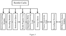
- Fig. 3 is a structure diagram of the vector computing device provided by the embodiments of the subject disclosure.
- the device comprises an instruction fetching module, a decoding module, an instruction queue, a scalar register file, a dependency relationship processing unit, a storage queue, a reorder buffer, a vector operations unit, a Scratchpad Memory, and an IO memory access module;
- the instruction fetching module is responsible for fetching the next instruction to be executed from the instruction sequence and transmitting the instruction to the decoding module;
- the decoding module is responsible for decoding the instruction and transmitting the decoded instruction to the instruction queue;
- the instruction queue is responsible for: considering the possible dependency relationship between different instructions on the scalar register, caching the decoded instruction and then sending the instruction when the dependency relationship is satisfied.
- the scalar register file is to provide the device with scalar register as needed in operations
- the dependency relationship processing unit is responsible for processing the possible storage dependency relationship between the instruction to be processed and its previous instruction.
- the vector operation instruction would access the Scratchpad Memory, and successive instructions may access the same memory space.
- the current instruction if detected to have a dependency relationship with data of the previous instruction, must wait within the storage queue until such dependency relationship is eliminated.
- the storage queue is a module with a sequential queue, wherein an instruction having a dependency relationship with the previous instruction in terms of data is stored in such queue until the dependency relationship is eliminated;
- the reorder buffer the instructions are cached in the reorder buffer while being executed. When execution of an instruction has been completed, if such instruction is also the earliest one among those instructions in the reorder buffer that have not been submitted, then it will be submitted; once such instruction is submitted, the status change of the device caused by execution of such instruction cannot be cancelled;
- the vector operations unit is responsible for all the vector operations of the device, including but not limited to vector addition operation, vector added to scalar operation, vector subtraction operation, scalar subtracted from vector operation, vector multiplication operation, vector multiplied by scalar operation, vector division (contrapuntally divided) operation, vector AND operation, and vector OR operation, and the vector operation instructions are sent to the operations unit for execution;
- the Scratchpad Memory is a temporary storage device specialized for vector data, and enabled to support vector data of different sizes;
- An IO memory access module is for directly accessing the Scratchpad Memory, and for reading or writing data from or into the Scratchpad Memory.
- Fig. 4 is a flowchart illustrating the process that the vector computing device provided by the embodiments of the subject disclosure executes a vector dot product instruction.
- the process of performing the vector dot product instruction (VP) comprises:
- the instruction fetching module retrieves the vector dot product instruction and transmits the instruction to the decoding module.
- S2 the decoding module decodes the instruction, and sends the instruction to the instruction queue.
- the vector dot product instruction needs to acquire from the scalar register file the data of the scalar register corresponding to four operation fields in the instruction, including starting address of vector vinO, length of vector vinO, starting address of vector vin1 and length of vector vin1.
- the instruction is sent to the dependency relationship processing unit.
- the dependency relationship processing unit analyzes whether there is a dependency relationship on data between the instruction and the previous instruction the execution of which has not been completed.
- the instruction needs to wait in the storage queue until it has no dependency relationship on data with the previous uncompleted instruction.
- the vector dot product instruction is transmitted to the vector operations unit.
- the vector operations unit retrieves the needed vectors from the data transient memory according to address and length of the needed data. Subsequently, the dot product operation is completed in the vector operations unit.
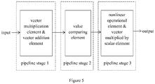
- Fig. 5 is a structure diagram of the vector operations unit provided by the embodiments of the subject disclosure.
- the vector operations unit comprises a vector addition operation unit, a value comparing unit, a nonlinear operation unit, and a vector multiplied by scalar unit.
- the vector operations unit is in the structure of multiple-stage pipeline, wherein the vector addition operation element and the vector multiplication element are arranged in pipeline stage 1, the value comparing element in stage 2, and the nonlinear operation element and the vector multiplied by scalar element in stage 3. Due to the difference of such elements in different stages of pipeline, when the order of the successive serial multiple vector operation instructions is consistent with pipeline order of the corresponding units, the operations as demanded by the series of vector operation instructions can be more effectively achieved.
Landscapes
- Engineering & Computer Science (AREA)
- Theoretical Computer Science (AREA)
- Software Systems (AREA)
- Physics & Mathematics (AREA)
- General Physics & Mathematics (AREA)
- General Engineering & Computer Science (AREA)
- Mathematical Physics (AREA)
- Mathematical Optimization (AREA)
- Pure & Applied Mathematics (AREA)
- Mathematical Analysis (AREA)
- Computational Mathematics (AREA)
- Data Mining & Analysis (AREA)
- Computing Systems (AREA)
- Algebra (AREA)
- Databases & Information Systems (AREA)
- Complex Calculations (AREA)
- Advance Control (AREA)
Applications Claiming Priority (2)
| Application Number | Priority Date | Filing Date | Title |
|---|---|---|---|
| CN201610039216.8A CN106990940B (zh) | 2016-01-20 | 2016-01-20 | 一种向量计算装置及运算方法 |
| PCT/CN2016/078550 WO2017124648A1 (fr) | 2016-01-20 | 2016-04-06 | Dispositif informatique de calcul de vecteur |
Publications (3)
| Publication Number | Publication Date |
|---|---|
| EP3407182A1 true EP3407182A1 (fr) | 2018-11-28 |
| EP3407182A4 EP3407182A4 (fr) | 2020-04-29 |
| EP3407182B1 EP3407182B1 (fr) | 2022-10-26 |
Family
ID=59361389
Family Applications (1)
| Application Number | Title | Priority Date | Filing Date |
|---|---|---|---|
| EP16885912.2A Active EP3407182B1 (fr) | 2016-01-20 | 2016-04-06 | Dispositif informatique de calcul de vecteur |
Country Status (4)
| Country | Link |
|---|---|
| EP (1) | EP3407182B1 (fr) |
| KR (3) | KR20180100550A (fr) |
| CN (5) | CN111580865B (fr) |
| WO (1) | WO2017124648A1 (fr) |
Families Citing this family (22)
| Publication number | Priority date | Publication date | Assignee | Title |
|---|---|---|---|---|
| CN107832843B (zh) * | 2017-10-30 | 2021-09-21 | 上海寒武纪信息科技有限公司 | 一种信息处理方法及相关产品 |
| CN109754062B (zh) * | 2017-11-07 | 2024-05-14 | 上海寒武纪信息科技有限公司 | 卷积扩展指令的执行方法以及相关产品 |
| CN109754061B (zh) * | 2017-11-07 | 2023-11-24 | 上海寒武纪信息科技有限公司 | 卷积扩展指令的执行方法以及相关产品 |
| CN107861757B (zh) * | 2017-11-30 | 2020-08-25 | 上海寒武纪信息科技有限公司 | 运算装置以及相关产品 |
| CN107957976B (zh) * | 2017-12-15 | 2020-12-18 | 安徽寒武纪信息科技有限公司 | 一种计算方法及相关产品 |
| CN108037908B (zh) * | 2017-12-15 | 2021-02-09 | 中科寒武纪科技股份有限公司 | 一种计算方法及相关产品 |
| CN108388446A (zh) * | 2018-02-05 | 2018-08-10 | 上海寒武纪信息科技有限公司 | 运算模块以及方法 |
| US12094456B2 (en) | 2018-09-13 | 2024-09-17 | Shanghai Cambricon Information Technology Co., Ltd. | Information processing method and system |
| CN110941789B (zh) * | 2018-09-21 | 2023-12-15 | 北京地平线机器人技术研发有限公司 | 张量运算方法和装置 |
| CN111290789B (zh) * | 2018-12-06 | 2022-05-27 | 上海寒武纪信息科技有限公司 | 运算方法、装置、计算机设备和存储介质 |
| CN111290788B (zh) * | 2018-12-07 | 2022-05-31 | 上海寒武纪信息科技有限公司 | 运算方法、装置、计算机设备和存储介质 |
| CN111079913B (zh) * | 2018-10-19 | 2021-02-05 | 中科寒武纪科技股份有限公司 | 运算方法、装置及相关产品 |
| CN111078282B (zh) * | 2018-10-19 | 2020-12-22 | 安徽寒武纪信息科技有限公司 | 运算方法、装置及相关产品 |
| CN111078281B (zh) * | 2018-10-19 | 2021-02-12 | 中科寒武纪科技股份有限公司 | 运算方法、系统及相关产品 |
| CN111079909B (zh) * | 2018-10-19 | 2021-01-26 | 安徽寒武纪信息科技有限公司 | 运算方法、系统及相关产品 |
| CN111399905B (zh) * | 2019-01-02 | 2022-08-16 | 上海寒武纪信息科技有限公司 | 运算方法、装置及相关产品 |
| US11507374B2 (en) * | 2019-05-20 | 2022-11-22 | Micron Technology, Inc. | True/false vector index registers and methods of populating thereof |
| US11403256B2 (en) | 2019-05-20 | 2022-08-02 | Micron Technology, Inc. | Conditional operations in a vector processor having true and false vector index registers |
| CN110502278B (zh) * | 2019-07-24 | 2021-07-16 | 瑞芯微电子股份有限公司 | 基于RiscV扩展指令的神经网络协处理器及其协处理方法 |
| US11494734B2 (en) * | 2019-09-11 | 2022-11-08 | Ila Design Group Llc | Automatically determining inventory items that meet selection criteria in a high-dimensionality inventory dataset |
| CN112633505B (zh) | 2020-12-24 | 2022-05-27 | 苏州浪潮智能科技有限公司 | 一种基于risc-v的人工智能推理方法和系统 |
| CN119045894B (zh) * | 2024-07-29 | 2025-12-12 | 武汉大学 | 多标量乘法运算方法、装置、设备及存储介质 |
Family Cites Families (30)
| Publication number | Priority date | Publication date | Assignee | Title |
|---|---|---|---|---|
| US4541046A (en) * | 1981-03-25 | 1985-09-10 | Hitachi, Ltd. | Data processing system including scalar data processor and vector data processor |
| JP3317985B2 (ja) * | 1991-11-20 | 2002-08-26 | 喜三郎 中澤 | 擬似ベクトルプロセッサ |
| US5669013A (en) * | 1993-10-05 | 1997-09-16 | Fujitsu Limited | System for transferring M elements X times and transferring N elements one time for an array that is X*M+N long responsive to vector type instructions |
| US5689653A (en) * | 1995-02-06 | 1997-11-18 | Hewlett-Packard Company | Vector memory operations |
| JPH09325888A (ja) * | 1996-06-04 | 1997-12-16 | Hitachi Ltd | データ処理装置 |
| US6665790B1 (en) * | 2000-02-29 | 2003-12-16 | International Business Machines Corporation | Vector register file with arbitrary vector addressing |
| CN1142484C (zh) * | 2001-11-28 | 2004-03-17 | 中国人民解放军国防科学技术大学 | 微处理器向量处理方法 |
| US20130212353A1 (en) * | 2002-02-04 | 2013-08-15 | Tibet MIMAR | System for implementing vector look-up table operations in a SIMD processor |
| JP4349265B2 (ja) * | 2004-11-22 | 2009-10-21 | ソニー株式会社 | プロセッサ |
| JP4282682B2 (ja) * | 2006-04-12 | 2009-06-24 | エヌイーシーコンピュータテクノ株式会社 | 情報処理装置及びそれに用いるベクトルレジスタアドレス制御方法 |
| US8108652B1 (en) * | 2007-09-13 | 2012-01-31 | Ronald Chi-Chun Hui | Vector processing with high execution throughput |
| JP5573134B2 (ja) * | 2009-12-04 | 2014-08-20 | 日本電気株式会社 | ベクトル型計算機及びベクトル型計算機の命令制御方法 |
| CN101833441B (zh) * | 2010-04-28 | 2013-02-13 | 中国科学院自动化研究所 | 并行向量处理引擎结构 |
| CN101876892B (zh) * | 2010-05-20 | 2013-07-31 | 复旦大学 | 面向通信和多媒体应用的单指令多数据处理器电路结构 |
| JP5658945B2 (ja) * | 2010-08-24 | 2015-01-28 | オリンパス株式会社 | 画像処理装置、画像処理装置の作動方法、および画像処理プログラム |
| CN102043723B (zh) * | 2011-01-06 | 2012-08-22 | 中国人民解放军国防科学技术大学 | 用于通用流处理器的可变访存模式的片上缓存结构 |
| CN102109978A (zh) * | 2011-02-28 | 2011-06-29 | 孙瑞琛 | 一种数据的重排方法及重排装置 |
| CN102156637A (zh) * | 2011-05-04 | 2011-08-17 | 中国人民解放军国防科学技术大学 | 向量交叉多线程处理方法及向量交叉多线程微处理器 |
| CN102200964B (zh) * | 2011-06-17 | 2013-05-15 | 孙瑞琛 | 基于并行处理的fft装置及其方法 |
| CN102262525B (zh) * | 2011-08-29 | 2014-11-19 | 孙瑞玮 | 基于矢量运算的矢量浮点运算装置及方法 |
| CN102495721A (zh) * | 2011-12-02 | 2012-06-13 | 南京大学 | 一种支持fft加速的simd向量处理器 |
| CN102750133B (zh) * | 2012-06-20 | 2014-07-30 | 中国电子科技集团公司第五十八研究所 | 支持simd的32位三发射的数字信号处理器 |
| US9098265B2 (en) * | 2012-07-11 | 2015-08-04 | Arm Limited | Controlling an order for processing data elements during vector processing |
| CN103699360B (zh) * | 2012-09-27 | 2016-09-21 | 北京中科晶上科技有限公司 | 一种向量处理器及其进行向量数据存取、交互的方法 |
| US9632781B2 (en) * | 2013-02-26 | 2017-04-25 | Qualcomm Incorporated | Vector register addressing and functions based on a scalar register data value |
| US9639503B2 (en) * | 2013-03-15 | 2017-05-02 | Qualcomm Incorporated | Vector indirect element vertical addressing mode with horizontal permute |
| KR20150005062A (ko) * | 2013-07-04 | 2015-01-14 | 삼성전자주식회사 | 미니-코어를 사용하는 프로세서 |
| US10120682B2 (en) * | 2014-02-28 | 2018-11-06 | International Business Machines Corporation | Virtualization in a bi-endian-mode processor architecture |
| CN104699465B (zh) * | 2015-03-26 | 2017-05-24 | 中国人民解放军国防科学技术大学 | 向量处理器中支持simt的向量访存装置和控制方法 |
| CN104699458A (zh) * | 2015-03-30 | 2015-06-10 | 哈尔滨工业大学 | 定点向量处理器及其向量数据访存控制方法 |
-
2016
- 2016-01-20 CN CN202010318480.1A patent/CN111580865B/zh active Active
- 2016-01-20 CN CN201610039216.8A patent/CN106990940B/zh active Active
- 2016-01-20 CN CN202010318896.3A patent/CN111580866B/zh active Active
- 2016-01-20 CN CN202010317170.8A patent/CN111580863B/zh active Active
- 2016-01-20 CN CN202010318173.3A patent/CN111580864B/zh active Active
- 2016-04-06 KR KR1020187015435A patent/KR20180100550A/ko not_active Ceased
- 2016-04-06 EP EP16885912.2A patent/EP3407182B1/fr active Active
- 2016-04-06 KR KR1020207013258A patent/KR102304216B1/ko active Active
- 2016-04-06 KR KR1020197017258A patent/KR102185287B1/ko active Active
- 2016-04-06 WO PCT/CN2016/078550 patent/WO2017124648A1/fr not_active Ceased
Also Published As
| Publication number | Publication date |
|---|---|
| CN111580864A (zh) | 2020-08-25 |
| CN111580866B (zh) | 2024-05-07 |
| KR20180100550A (ko) | 2018-09-11 |
| CN111580865A (zh) | 2020-08-25 |
| CN111580863A (zh) | 2020-08-25 |
| CN106990940A (zh) | 2017-07-28 |
| CN111580863B (zh) | 2024-05-03 |
| KR20200058562A (ko) | 2020-05-27 |
| EP3407182B1 (fr) | 2022-10-26 |
| CN106990940B (zh) | 2020-05-22 |
| KR102185287B1 (ko) | 2020-12-01 |
| KR102304216B1 (ko) | 2021-09-23 |
| CN111580864B (zh) | 2024-05-07 |
| CN111580865B (zh) | 2024-02-27 |
| EP3407182A4 (fr) | 2020-04-29 |
| KR20190073593A (ko) | 2019-06-26 |
| WO2017124648A1 (fr) | 2017-07-27 |
| CN111580866A (zh) | 2020-08-25 |
Similar Documents
| Publication | Publication Date | Title |
|---|---|---|
| EP3407182B1 (fr) | Dispositif informatique de calcul de vecteur | |
| EP3407202A1 (fr) | Appareil de calcul de matrice | |
| CN111310910B (zh) | 一种计算装置及方法 | |
| CN111651205B (zh) | 一种用于执行向量内积运算的装置和方法 | |
| CN107315717B (zh) | 一种用于执行向量四则运算的装置和方法 | |
| CN107315715B (zh) | 一种用于执行矩阵加/减运算的装置和方法 | |
| CN111651206B (zh) | 一种用于执行向量外积运算的装置和方法 | |
| CN107315574A (zh) | 一种用于执行矩阵乘运算的装置和方法 | |
| CN111651202B (zh) | 一种用于执行向量逻辑运算的装置 | |
| EP3447690A1 (fr) | Appareil et procédé d'opération de couche "maxout" | |
| CN111651204A (zh) | 一种用于执行向量最大值最小值运算的装置和方法 | |
| CN112348182B (zh) | 一种神经网络maxout层计算装置 |
Legal Events
| Date | Code | Title | Description |
|---|---|---|---|
| STAA | Information on the status of an ep patent application or granted ep patent |
Free format text: STATUS: THE INTERNATIONAL PUBLICATION HAS BEEN MADE |
|
| PUAI | Public reference made under article 153(3) epc to a published international application that has entered the european phase |
Free format text: ORIGINAL CODE: 0009012 |
|
| STAA | Information on the status of an ep patent application or granted ep patent |
Free format text: STATUS: REQUEST FOR EXAMINATION WAS MADE |
|
| 17P | Request for examination filed |
Effective date: 20180531 |
|
| AK | Designated contracting states |
Kind code of ref document: A1 Designated state(s): AL AT BE BG CH CY CZ DE DK EE ES FI FR GB GR HR HU IE IS IT LI LT LU LV MC MK MT NL NO PL PT RO RS SE SI SK SM TR |
|
| AX | Request for extension of the european patent |
Extension state: BA ME |
|
| DAV | Request for validation of the european patent (deleted) | ||
| DAX | Request for extension of the european patent (deleted) | ||
| A4 | Supplementary search report drawn up and despatched |
Effective date: 20200401 |
|
| RIC1 | Information provided on ipc code assigned before grant |
Ipc: G06F 9/30 20180101AFI20200326BHEP Ipc: G06F 9/35 20180101ALI20200326BHEP Ipc: G06F 9/38 20180101ALI20200326BHEP |
|
| STAA | Information on the status of an ep patent application or granted ep patent |
Free format text: STATUS: EXAMINATION IS IN PROGRESS |
|
| 17Q | First examination report despatched |
Effective date: 20200609 |
|
| GRAP | Despatch of communication of intention to grant a patent |
Free format text: ORIGINAL CODE: EPIDOSNIGR1 |
|
| STAA | Information on the status of an ep patent application or granted ep patent |
Free format text: STATUS: GRANT OF PATENT IS INTENDED |
|
| INTG | Intention to grant announced |
Effective date: 20220520 |
|
| RAP3 | Party data changed (applicant data changed or rights of an application transferred) |
Owner name: CAMBRICON TECHNOLOGIES CORPORATION LIMITED |
|
| RIN1 | Information on inventor provided before grant (corrected) |
Inventor name: CHEN, YUNJI Inventor name: LIU, SHAOLI Inventor name: ZHANG, XIAO Inventor name: CHEN, TIANSHI |
|
| GRAS | Grant fee paid |
Free format text: ORIGINAL CODE: EPIDOSNIGR3 |
|
| GRAA | (expected) grant |
Free format text: ORIGINAL CODE: 0009210 |
|
| STAA | Information on the status of an ep patent application or granted ep patent |
Free format text: STATUS: THE PATENT HAS BEEN GRANTED |
|
| AK | Designated contracting states |
Kind code of ref document: B1 Designated state(s): AL AT BE BG CH CY CZ DE DK EE ES FI FR GB GR HR HU IE IS IT LI LT LU LV MC MK MT NL NO PL PT RO RS SE SI SK SM TR |
|
| RAP1 | Party data changed (applicant data changed or rights of an application transferred) |
Owner name: CAMBRICON (XI'AN) SEMICONDUCTOR CO., LTD. |
|
| REG | Reference to a national code |
Ref country code: GB Ref legal event code: FG4D |
|
| REG | Reference to a national code |
Ref country code: CH Ref legal event code: EP |
|
| REG | Reference to a national code |
Ref country code: AT Ref legal event code: REF Ref document number: 1527534 Country of ref document: AT Kind code of ref document: T Effective date: 20221115 |
|
| REG | Reference to a national code |
Ref country code: DE Ref legal event code: R096 Ref document number: 602016075970 Country of ref document: DE |
|
| REG | Reference to a national code |
Ref country code: IE Ref legal event code: FG4D |
|
| REG | Reference to a national code |
Ref country code: LT Ref legal event code: MG9D |
|
| REG | Reference to a national code |
Ref country code: NL Ref legal event code: MP Effective date: 20221026 |
|
| REG | Reference to a national code |
Ref country code: AT Ref legal event code: MK05 Ref document number: 1527534 Country of ref document: AT Kind code of ref document: T Effective date: 20221026 |
|
| PG25 | Lapsed in a contracting state [announced via postgrant information from national office to epo] |
Ref country code: NL Free format text: LAPSE BECAUSE OF FAILURE TO SUBMIT A TRANSLATION OF THE DESCRIPTION OR TO PAY THE FEE WITHIN THE PRESCRIBED TIME-LIMIT Effective date: 20221026 |
|
| PG25 | Lapsed in a contracting state [announced via postgrant information from national office to epo] |
Ref country code: SE Free format text: LAPSE BECAUSE OF FAILURE TO SUBMIT A TRANSLATION OF THE DESCRIPTION OR TO PAY THE FEE WITHIN THE PRESCRIBED TIME-LIMIT Effective date: 20221026 Ref country code: PT Free format text: LAPSE BECAUSE OF FAILURE TO SUBMIT A TRANSLATION OF THE DESCRIPTION OR TO PAY THE FEE WITHIN THE PRESCRIBED TIME-LIMIT Effective date: 20230227 Ref country code: NO Free format text: LAPSE BECAUSE OF FAILURE TO SUBMIT A TRANSLATION OF THE DESCRIPTION OR TO PAY THE FEE WITHIN THE PRESCRIBED TIME-LIMIT Effective date: 20230126 Ref country code: LT Free format text: LAPSE BECAUSE OF FAILURE TO SUBMIT A TRANSLATION OF THE DESCRIPTION OR TO PAY THE FEE WITHIN THE PRESCRIBED TIME-LIMIT Effective date: 20221026 Ref country code: FI Free format text: LAPSE BECAUSE OF FAILURE TO SUBMIT A TRANSLATION OF THE DESCRIPTION OR TO PAY THE FEE WITHIN THE PRESCRIBED TIME-LIMIT Effective date: 20221026 Ref country code: ES Free format text: LAPSE BECAUSE OF FAILURE TO SUBMIT A TRANSLATION OF THE DESCRIPTION OR TO PAY THE FEE WITHIN THE PRESCRIBED TIME-LIMIT Effective date: 20221026 Ref country code: AT Free format text: LAPSE BECAUSE OF FAILURE TO SUBMIT A TRANSLATION OF THE DESCRIPTION OR TO PAY THE FEE WITHIN THE PRESCRIBED TIME-LIMIT Effective date: 20221026 |
|
| PG25 | Lapsed in a contracting state [announced via postgrant information from national office to epo] |
Ref country code: RS Free format text: LAPSE BECAUSE OF FAILURE TO SUBMIT A TRANSLATION OF THE DESCRIPTION OR TO PAY THE FEE WITHIN THE PRESCRIBED TIME-LIMIT Effective date: 20221026 Ref country code: PL Free format text: LAPSE BECAUSE OF FAILURE TO SUBMIT A TRANSLATION OF THE DESCRIPTION OR TO PAY THE FEE WITHIN THE PRESCRIBED TIME-LIMIT Effective date: 20221026 Ref country code: LV Free format text: LAPSE BECAUSE OF FAILURE TO SUBMIT A TRANSLATION OF THE DESCRIPTION OR TO PAY THE FEE WITHIN THE PRESCRIBED TIME-LIMIT Effective date: 20221026 Ref country code: IS Free format text: LAPSE BECAUSE OF FAILURE TO SUBMIT A TRANSLATION OF THE DESCRIPTION OR TO PAY THE FEE WITHIN THE PRESCRIBED TIME-LIMIT Effective date: 20230226 Ref country code: HR Free format text: LAPSE BECAUSE OF FAILURE TO SUBMIT A TRANSLATION OF THE DESCRIPTION OR TO PAY THE FEE WITHIN THE PRESCRIBED TIME-LIMIT Effective date: 20221026 Ref country code: GR Free format text: LAPSE BECAUSE OF FAILURE TO SUBMIT A TRANSLATION OF THE DESCRIPTION OR TO PAY THE FEE WITHIN THE PRESCRIBED TIME-LIMIT Effective date: 20230127 |
|
| REG | Reference to a national code |
Ref country code: DE Ref legal event code: R097 Ref document number: 602016075970 Country of ref document: DE |
|
| PG25 | Lapsed in a contracting state [announced via postgrant information from national office to epo] |
Ref country code: SM Free format text: LAPSE BECAUSE OF FAILURE TO SUBMIT A TRANSLATION OF THE DESCRIPTION OR TO PAY THE FEE WITHIN THE PRESCRIBED TIME-LIMIT Effective date: 20221026 Ref country code: RO Free format text: LAPSE BECAUSE OF FAILURE TO SUBMIT A TRANSLATION OF THE DESCRIPTION OR TO PAY THE FEE WITHIN THE PRESCRIBED TIME-LIMIT Effective date: 20221026 Ref country code: EE Free format text: LAPSE BECAUSE OF FAILURE TO SUBMIT A TRANSLATION OF THE DESCRIPTION OR TO PAY THE FEE WITHIN THE PRESCRIBED TIME-LIMIT Effective date: 20221026 Ref country code: DK Free format text: LAPSE BECAUSE OF FAILURE TO SUBMIT A TRANSLATION OF THE DESCRIPTION OR TO PAY THE FEE WITHIN THE PRESCRIBED TIME-LIMIT Effective date: 20221026 Ref country code: CZ Free format text: LAPSE BECAUSE OF FAILURE TO SUBMIT A TRANSLATION OF THE DESCRIPTION OR TO PAY THE FEE WITHIN THE PRESCRIBED TIME-LIMIT Effective date: 20221026 |
|
| PG25 | Lapsed in a contracting state [announced via postgrant information from national office to epo] |
Ref country code: SK Free format text: LAPSE BECAUSE OF FAILURE TO SUBMIT A TRANSLATION OF THE DESCRIPTION OR TO PAY THE FEE WITHIN THE PRESCRIBED TIME-LIMIT Effective date: 20221026 Ref country code: AL Free format text: LAPSE BECAUSE OF FAILURE TO SUBMIT A TRANSLATION OF THE DESCRIPTION OR TO PAY THE FEE WITHIN THE PRESCRIBED TIME-LIMIT Effective date: 20221026 |
|
| PLBE | No opposition filed within time limit |
Free format text: ORIGINAL CODE: 0009261 |
|
| STAA | Information on the status of an ep patent application or granted ep patent |
Free format text: STATUS: NO OPPOSITION FILED WITHIN TIME LIMIT |
|
| 26N | No opposition filed |
Effective date: 20230727 |
|
| PG25 | Lapsed in a contracting state [announced via postgrant information from national office to epo] |
Ref country code: SI Free format text: LAPSE BECAUSE OF FAILURE TO SUBMIT A TRANSLATION OF THE DESCRIPTION OR TO PAY THE FEE WITHIN THE PRESCRIBED TIME-LIMIT Effective date: 20221026 |
|
| REG | Reference to a national code |
Ref country code: CH Ref legal event code: PL |
|
| PG25 | Lapsed in a contracting state [announced via postgrant information from national office to epo] |
Ref country code: LU Free format text: LAPSE BECAUSE OF NON-PAYMENT OF DUE FEES Effective date: 20230406 |
|
| REG | Reference to a national code |
Ref country code: BE Ref legal event code: MM Effective date: 20230430 |
|
| PG25 | Lapsed in a contracting state [announced via postgrant information from national office to epo] |
Ref country code: MC Free format text: LAPSE BECAUSE OF FAILURE TO SUBMIT A TRANSLATION OF THE DESCRIPTION OR TO PAY THE FEE WITHIN THE PRESCRIBED TIME-LIMIT Effective date: 20221026 |
|
| PG25 | Lapsed in a contracting state [announced via postgrant information from national office to epo] |
Ref country code: MC Free format text: LAPSE BECAUSE OF FAILURE TO SUBMIT A TRANSLATION OF THE DESCRIPTION OR TO PAY THE FEE WITHIN THE PRESCRIBED TIME-LIMIT Effective date: 20221026 Ref country code: LI Free format text: LAPSE BECAUSE OF NON-PAYMENT OF DUE FEES Effective date: 20230430 Ref country code: CH Free format text: LAPSE BECAUSE OF NON-PAYMENT OF DUE FEES Effective date: 20230430 |
|
| REG | Reference to a national code |
Ref country code: IE Ref legal event code: MM4A |
|
| PG25 | Lapsed in a contracting state [announced via postgrant information from national office to epo] |
Ref country code: BE Free format text: LAPSE BECAUSE OF NON-PAYMENT OF DUE FEES Effective date: 20230430 |
|
| PG25 | Lapsed in a contracting state [announced via postgrant information from national office to epo] |
Ref country code: IE Free format text: LAPSE BECAUSE OF NON-PAYMENT OF DUE FEES Effective date: 20230406 |
|
| PG25 | Lapsed in a contracting state [announced via postgrant information from national office to epo] |
Ref country code: IE Free format text: LAPSE BECAUSE OF NON-PAYMENT OF DUE FEES Effective date: 20230406 |
|
| PG25 | Lapsed in a contracting state [announced via postgrant information from national office to epo] |
Ref country code: IT Free format text: LAPSE BECAUSE OF FAILURE TO SUBMIT A TRANSLATION OF THE DESCRIPTION OR TO PAY THE FEE WITHIN THE PRESCRIBED TIME-LIMIT Effective date: 20221026 |
|
| PG25 | Lapsed in a contracting state [announced via postgrant information from national office to epo] |
Ref country code: BG Free format text: LAPSE BECAUSE OF FAILURE TO SUBMIT A TRANSLATION OF THE DESCRIPTION OR TO PAY THE FEE WITHIN THE PRESCRIBED TIME-LIMIT Effective date: 20221026 |
|
| PG25 | Lapsed in a contracting state [announced via postgrant information from national office to epo] |
Ref country code: BG Free format text: LAPSE BECAUSE OF FAILURE TO SUBMIT A TRANSLATION OF THE DESCRIPTION OR TO PAY THE FEE WITHIN THE PRESCRIBED TIME-LIMIT Effective date: 20221026 |
|
| PGFP | Annual fee paid to national office [announced via postgrant information from national office to epo] |
Ref country code: DE Payment date: 20250422 Year of fee payment: 10 |
|
| PGFP | Annual fee paid to national office [announced via postgrant information from national office to epo] |
Ref country code: FR Payment date: 20250425 Year of fee payment: 10 |
|
| PG25 | Lapsed in a contracting state [announced via postgrant information from national office to epo] |
Ref country code: CY Free format text: LAPSE BECAUSE OF FAILURE TO SUBMIT A TRANSLATION OF THE DESCRIPTION OR TO PAY THE FEE WITHIN THE PRESCRIBED TIME-LIMIT; INVALID AB INITIO Effective date: 20160406 |
|
| PG25 | Lapsed in a contracting state [announced via postgrant information from national office to epo] |
Ref country code: HU Free format text: LAPSE BECAUSE OF FAILURE TO SUBMIT A TRANSLATION OF THE DESCRIPTION OR TO PAY THE FEE WITHIN THE PRESCRIBED TIME-LIMIT; INVALID AB INITIO Effective date: 20160406 |
|
| PG25 | Lapsed in a contracting state [announced via postgrant information from national office to epo] |
Ref country code: TR Free format text: LAPSE BECAUSE OF FAILURE TO SUBMIT A TRANSLATION OF THE DESCRIPTION OR TO PAY THE FEE WITHIN THE PRESCRIBED TIME-LIMIT Effective date: 20221026 |
|
| PGFP | Annual fee paid to national office [announced via postgrant information from national office to epo] |
Ref country code: GB Payment date: 20260313 Year of fee payment: 11 |