EP3410251B1 - Spannungsregler mit laststromvorhersage und verfahren dafür - Google Patents
Spannungsregler mit laststromvorhersage und verfahren dafür Download PDFInfo
- Publication number
- EP3410251B1 EP3410251B1 EP18173659.6A EP18173659A EP3410251B1 EP 3410251 B1 EP3410251 B1 EP 3410251B1 EP 18173659 A EP18173659 A EP 18173659A EP 3410251 B1 EP3410251 B1 EP 3410251B1
- Authority
- EP
- European Patent Office
- Prior art keywords
- terminal
- voltage
- control
- coupled
- transistor
- Prior art date
- Legal status (The legal status is an assumption and is not a legal conclusion. Google has not performed a legal analysis and makes no representation as to the accuracy of the status listed.)
- Not-in-force
Links
Images


Classifications
-
- H—ELECTRICITY
- H02—GENERATION; CONVERSION OR DISTRIBUTION OF ELECTRIC POWER
- H02M—APPARATUS FOR CONVERSION BETWEEN AC AND AC, BETWEEN AC AND DC, OR BETWEEN DC AND DC, AND FOR USE WITH MAINS OR SIMILAR POWER SUPPLY SYSTEMS; CONVERSION OF DC OR AC INPUT POWER INTO SURGE OUTPUT POWER; CONTROL OR REGULATION THEREOF
- H02M3/00—Conversion of DC power input into DC power output
- H02M3/02—Conversion of DC power input into DC power output without intermediate conversion into AC
- H02M3/04—Conversion of DC power input into DC power output without intermediate conversion into AC by static converters
- H02M3/06—Conversion of DC power input into DC power output without intermediate conversion into AC by static converters using resistors or capacitors, e.g. potential divider
- H02M3/07—Conversion of DC power input into DC power output without intermediate conversion into AC by static converters using resistors or capacitors, e.g. potential divider using capacitors charged and discharged alternately by semiconductor devices with control electrode, e.g. charge pumps
-
- G—PHYSICS
- G05—CONTROLLING; REGULATING
- G05F—SYSTEMS FOR REGULATING ELECTRIC OR MAGNETIC VARIABLES
- G05F1/00—Automatic systems in which deviations of an electric quantity from one or more predetermined values are detected at the output of the system and fed back to a device within the system to restore the detected quantity to its predetermined value or values, i.e. retroactive systems
- G05F1/10—Regulating voltage or current
- G05F1/46—Regulating voltage or current wherein the variable actually regulated by the final control device is DC
- G05F1/462—Regulating voltage or current wherein the variable actually regulated by the final control device is DC as a function of the requirements of the load, e.g. delay, temperature, specific voltage/current characteristic
-
- G—PHYSICS
- G05—CONTROLLING; REGULATING
- G05F—SYSTEMS FOR REGULATING ELECTRIC OR MAGNETIC VARIABLES
- G05F1/00—Automatic systems in which deviations of an electric quantity from one or more predetermined values are detected at the output of the system and fed back to a device within the system to restore the detected quantity to its predetermined value or values, i.e. retroactive systems
- G05F1/10—Regulating voltage or current
- G05F1/46—Regulating voltage or current wherein the variable actually regulated by the final control device is DC
- G05F1/56—Regulating voltage or current wherein the variable actually regulated by the final control device is DC using semiconductor devices in series with the load as final control devices
- G05F1/565—Regulating voltage or current wherein the variable actually regulated by the final control device is DC using semiconductor devices in series with the load as final control devices sensing a condition of the system or its load in addition to means responsive to deviations in the output of the system, e.g. current, voltage, power factor
-
- G—PHYSICS
- G05—CONTROLLING; REGULATING
- G05F—SYSTEMS FOR REGULATING ELECTRIC OR MAGNETIC VARIABLES
- G05F1/00—Automatic systems in which deviations of an electric quantity from one or more predetermined values are detected at the output of the system and fed back to a device within the system to restore the detected quantity to its predetermined value or values, i.e. retroactive systems
- G05F1/10—Regulating voltage or current
- G05F1/46—Regulating voltage or current wherein the variable actually regulated by the final control device is DC
- G05F1/56—Regulating voltage or current wherein the variable actually regulated by the final control device is DC using semiconductor devices in series with the load as final control devices
- G05F1/575—Regulating voltage or current wherein the variable actually regulated by the final control device is DC using semiconductor devices in series with the load as final control devices characterised by the feedback circuit
Definitions
- This disclosure relates generally to electrical circuits, and more specifically, to a voltage regulator with load current prediction and method therefor.
- FIG. 1 illustrates, in schematic diagram form, a pin-less voltage regulator 10 in accordance with the prior art.
- FIG. 1 shows an example implementation of a switched biasing control circuit 12 connected to N-channel transistor 14.
- N-channel transistor 14 has an intrinsic gate-source capacitance represented by capacitor 16 in FIG. 1 .
- Capacitor 16 also represents all other capacitances connected to the gate of N-channel transistor 14.
- Biasing control circuit 12 is composed of two comparators 18 and 20 in a window comparison configuration.
- Comparator 18 receives a reference voltage labeled VREF_LO and controls the gate of P-channel transistor 22 in response to a comparison of VREF_LO with a feedback voltage generated from an output voltage VOUT.
- Comparator 20 receives a reference voltage labeled VREF_HI and provides a bias voltage to control the gate of N-channel transistor 28 in response to a comparison of VREF_HI with the feedback voltage generated from output voltage VOUT.
- N-channel transistor 14 drives a variable load that can be modelled by a resistance 30 and a capacitance 32.
- Biasing control circuit 12 controls the conductivity of N-channel transistor 14 in response to a changing load sensed via the feedback of VOUT.
- the reference voltages are used to set the voltage of VOUT.
- Reference voltage VREF_LO is lower than reference voltage VREF_HI.
- the output voltage variation is a percentage of nominal supply voltage.
- the nominal supply voltage is reduced.
- the power supply voltage may be 1.25 volts and at the 28 nm technology node the power supply voltage may be 0.9 volts.
- the voltage variation in absolute value, not in percentage was also reduced at the newer technology nodes, reducing the margin for regulator accuracy and voltage variation due to load steps.
- the low power techniques power gating, clock gating, back biasing technique greatly increase the load transient current steps. Using these low power techniques, the load transient current steps may reach up to 1000x.
- voltage regulator 10 may not be able to detect and react to the faster load current steps. Also, for a fixed gate voltage if the source voltage VDD decreases, the current flowing through N-channel transistor 14 will increase to minimize source voltage drop. However, it takes time for the VOUT feedback voltage to be reacted to by biasing control 12, thus allowing a significant output voltage drop before bias circuit 12 can react to the load change.
- a voltage regulator according to claim 1 In a first aspect there is provided a voltage regulator according to claim 1. In a second aspect there is provided a voltage regulator according to claim 2. In a third aspect there is provided a voltage regulator according to claim 3.
- a voltage regulator implemented in an integrated circuit data processing system.
- the voltage regulator includes a transistor, a feedback circuit, a charge boosting circuit, and a load prediction circuit.
- the transistor has a first current electrode coupled to a first power supply voltage terminal, a second current electrode for providing a regulated output voltage, and a control electrode.
- the feedback circuit controls a bias voltage to the control electrode of the transistor in response to a feedback signal generated from the regulated output voltage.
- the charge boosting circuit transfers charge to the control electrode of the transistor in response to one or more control signals.
- the load prediction circuit is coupled to the charge boosting circuit.
- the load prediction circuit provides the control signal to the charge boosting circuit in response to determining that a load current at the second current electrode of the transistor is expected to increase.
- the load prediction circuit monitors the execution of instructions, and boosts the gate voltage of the transistor when instruction execution suggests an upcoming increase in the load supplied by the transistor.
- the load prediction circuit may monitor another aspect of data processing to predict an increase in load current.
- the first biasing circuit may comprise: a first comparator having a first input terminal for receiving a first reference voltage, a second input terminal coupled to receive the feedback signal, and an output terminal coupled to a first switch; and a second comparator having a first input terminal for receiving a second reference voltage, a second input terminal coupled to receive the feedback signal, and an output terminal coupled to a second switch.
- the transistor may be an N-channel metal-oxide semiconductor transistor and the first current electrode may be a drain and the second current electrode may be a source.
- the second biasing circuit may comprise: a capacitor having a first terminal coupled to the control electrode of the transistor, and a second terminal; a first switch having a first terminal coupled to the second terminal of the capacitor, a second terminal coupled to a second power supply voltage terminal, and a control terminal for receiving the first control signal from the load prediction circuit; and a second switch having a first terminal coupled to the second terminal of the capacitor, a second terminal coupled to a third power supply voltage terminal, and a control terminal coupled to receive the second control signal from the load prediction circuit.
- the first power supply voltage terminal may be for receiving a positive power supply voltage
- the second power supply voltage terminal may be for receiving a negative power supply voltage
- the third power supply voltage terminal may be for coupling to ground.
- the transistor may be an N-channel transistor operating in a subthreshold region.
- the load prediction circuit may predict the increase in load current by monitoring instructions being executed.
- the control signal may further comprise first and second control signals
- the charge boosting circuit may comprise: a first switch having a first terminal coupled to the control electrode of the transistor, a second terminal, and a control terminal for receiving the first control signal from the load prediction circuit; a capacitor having a first terminal coupled to the second terminal of the first switch, and a second terminal coupled to a second power supply terminal; and a second switch having a first terminal coupled to the first terminal of the capacitor, and a second terminal coupled to receive a first voltage, and a control terminal for receiving the second control signal from the load prediction circuit.
- the first power supply voltage terminal may be for receiving a positive power supply voltage
- the second power supply voltage terminal may be for receiving a negative power supply voltage
- the third power supply voltage terminal may be for coupling to a ground.
- the load prediction circuit may predict the increase in load current by monitoring instructions being executed.
- a method for providing a regulated output voltage to a load in an integrated circuit comprising: providing the regulated output voltage from a source terminal of an N-channel transistor; generating a feedback signal from the regulated output voltage; providing the feedback signal to first and second comparators for controlling a bias voltage provided to a gate of the N-channel transistor; and controlling a voltage boost circuit coupled to the gate of the N-channel transistor for boosting the bias voltage by a predetermined voltage in response to anticipating an increased load current to the load.
- Anticipating an increased load current to the load may further comprise anticipating an increased load current by monitoring instruction execution in the integrated circuit.
- Boosting the bias voltage by a predetermined voltage may further comprise using a capacitor to boost the bias voltage.
- Controlling the voltage boost circuit may comprise: precharging a capacitor; and coupling the capacitor to the gate of the N-channel transistor in response to anticipating of the increased load current.
- the method may further comprise operating the N-channel transistor in a subthreshold region.
- comparator 48 has a first input terminal labeled (+) for receiving reference voltage VREF_LO, a second input terminal labeled (-), and an output terminal.
- Comparator 50 has a first input terminal labeled (-) for receiving reference voltage VREF_HI, a second input terminal, and an output terminal.
- P-channel transistor 52 has a source connected to a power supply voltage terminal labeled VDD, a gate connected to the output terminal of comparator 48, and a drain.
- Current source 54 has a first terminal connected to the drain of P-channel transistor 52, and a second terminal.
- Current source 56 has a first terminal connected to the second terminal of current source 54, and a second terminal.
- the power supply voltage provided to power supply voltage terminal VDD is nominally about 0.9 volts, and power supply voltage terminal VSS is connected to ground.
- Voltage source V1 is a positive voltage that is greater than a maximum voltage that gate voltage VGATE can reach, and may be equal to the voltage at power supply voltage terminal VDD.
- Reference voltage VREF_LO is lower than reference voltage VREF_HI.
- Processor 44 may be any kind of processor and include one or more processing cores. Processor 44 may be a microcontroller, a microprocessor, a digital signal processor (DSP), or the like. In a CMOS processing technology, current source 54 may be implemented as a P-channel transistor biased with a predetermined bias voltage. Current source 56 may be implemented as an N-channel transistor biased with a predetermined bias voltage.
- biasing circuit 40 provides a charge boost to the gate of N-channel transistor 42 in response to anticipating that a load current demand to the load is going to increase.
- biasing circuit 40 may be implemented differently. Accordingly, in biasing circuit 40, switch 66 is closed by S2 to precharge capacitor 64 to V1 during a time when processor 44 is idle or in a steady state load condition.
- Activity control 46 monitors a processing activity of processor 44. When an indicator is received that indicates the load current for voltage regulator 35 is going to increase, load current prediction circuit 46 provides control signal S1 and S2 to the control terminals of switches 62 and 66, respectively. Switch 62 closes, connecting the charged capacitor 64 to the gate of N-channel transistor 42.
- the charge increases the gate voltage VGATE so that N-channel transistor 42 becomes more conductive and provides more current to supply the predicted increase in load current.
- voltage regulator 35 reduces the amount of voltage drop of VOUT that may be caused when the load current increases abruptly and biasing circuit 38 cannot react quickly enough to counter the voltage drop.
- the voltage boost is temporary provided by biasing circuit 40 and for a predetermined time period because it is provided from a charged capacitor, allowing biasing circuit 38 to take over and provide continued regulation as needed following the increased load current event.
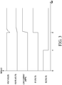
- FIG. 3 illustrates waveforms of various signals for a better understanding of the operation of voltage regulator 35 ( FIG. 2 ).
- the load current LOAD CURRENT is relatively constant and output voltage VOUT is normal.
- Control signal S1 is a logic low causing switch 62 to be open.
- Control signal S2 is asserted as a logic high, causing switch 66 to be closed.
- Voltage V1 is provided to the first terminal of capacitor 64, causing capacitor 64 to be precharged to about V1.
- the time after t0 capacitor 64 is charged and ready for an increase in load current.
- the voltage level of V1 and the size of capacitor 64 are chosen to provide a predetermined amount of voltage boost to gate voltage VGATE.
- switch 66 opens before switch 62 closes at time t1.
- voltage VGATE is boosted to compensate for the increased load current.
- voltage VOUT in voltage regulator 35 drops a smaller amount than it would have in voltage regulator 10 without load current prediction. In some embodiments, the improvement may be significant.
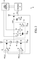
- FIG. 4 illustrates, in partial schematic diagram form and partial block diagram form, voltage regulator 37 in accordance with another embodiment.
- Voltage regulator 37 is the same as voltage regulator 35 except that biasing circuit 40 has been replaced with biasing circuit 70.
- Biasing circuit 70 includes capacitor 72, switches 74 and 78, and voltage source V2.
- Capacitor 72 has a first terminal connected to the gate of N-channel transistor 42, and a second terminal.
- Switch 74 has a first terminal connected to the second terminal of capacitor 72, a second terminal connected to receive a voltage V2, and a control terminal for receiving control signal S1.
- Voltage V2 is a negative voltage.
- Switch 78 has a first terminal connected to the second terminal of capacitor 72, a second terminal connected to VSS, and a control terminal for receiving control signal S2.
- Biasing circuit 70 works substantially the same as biasing circuit 40 in FIG. 2 , and may be desirable in an integrated circuit that has a negative voltage available.
- closing switch 74 causes capacitor 72 to be precharged and closing switch 78 after switch 74 is opened boosts gate voltage VGATE.
- the operation of voltage regulator 37 is substantially the same as the operation of voltage regulator 35 and as illustrated by the waveforms of FIG. 3 .
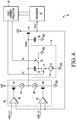
- FIG. 5 illustrates, in partial schematic diagram form and partial block diagram form, voltage regulator 39 in accordance with another embodiment.
- Voltage regulator 39 is the same as voltage regulator 35 except that biasing circuit 40 is replaced with biasing circuit 80.
- Biasing circuit 80 includes switches 82, 86, 88, and 90, and capacitor 84.
- Switch 82 has a first terminal connected to the gate of N-channel transistor 42, a second terminal, and a control terminal for receiving control signal S1.
- Capacitor 84 has a first terminal connected to the second terminal of switch 82, and a second terminal.
- Switch 86 has a first terminal connected to the second terminal of capacitor 84, a second terminal connected to receive VDD, and a control terminal for receiving control signal S1.
- Switch 88 has a first terminal connected to the first terminal of capacitor 84, a second terminal for receiving VDD, and a control terminal for receiving control signal S2.
- Switch 90 has a first terminal connected to the second terminal of capacitor 84, a second terminal connected to VSS, and a control terminal for receiving control signal S2.
- asserting control signal S2 precharges capacitor 84 and asserting control signal S1 after control signal S2 is negated causes the stored charge in capacitor 84 to boost the gate voltage VGATE.
- switches 88 and 90 are closed and switches 82 and 86 are open to precharge capacitor 84.
- boost voltage VGATE signal S2 is negated and signal S1 is asserted.
- switches 82 and 86 close, causing charged capacitor 84 to be connected between VDD the gate of N-channel transistor 42 to boost VGATE.
- the waveforms of FIG. 3 also illustrate the operation of voltage regulator 39.
- a current electrode is a source or drain and a control electrode is a gate of a metal-oxide semiconductor (MOS) transistor.
- MOS metal-oxide semiconductor
- Coupled is not intended to be limited to a direct coupling or a mechanical coupling.
Landscapes
- Engineering & Computer Science (AREA)
- Physics & Mathematics (AREA)
- Electromagnetism (AREA)
- General Physics & Mathematics (AREA)
- Radar, Positioning & Navigation (AREA)
- Automation & Control Theory (AREA)
- Power Engineering (AREA)
- Continuous-Control Power Sources That Use Transistors (AREA)
Claims (8)
- Spannungsregulierer (35), der Folgendes umfasst:einen Transistor (42), der eine erste Stromelektrode, die mit einem ersten Leistungsversorgungs-Spannungsanschluss gekoppelt ist, eine zweite Stromelektrode zum Bereitstellen einer regulierten Ausgangsspannung und eine Steuerelektrode aufweist;eine erste Vorspannungsschaltung (38) zum Bereitstellen einer ersten Vorspannung bei der Steuerelektrode des Transistors als Antwort auf ein Rückkopplungssignal, das aus der regulierten Ausgangsspannung erzeugt wird;eine zweite Vorspannungsschaltung (40) zum Bereitstellen einer zweiten Vorspannung bei der Steuerelektrode des Transistors als Antwort auf ein Steuersignal; undeine Laststrom-Vorhersageschaltung (46), die mit der zweiten Vorspannungsschaltung gekoppelt ist, wobei die Lastvorhersageschaltung zum Bereitstellen eines ersten und eines zweiten Steuersignals an die zweite Vorspannungsschaltung als Antwort auf das Bestimmen, dass erwartet wird, dass ein Laststrom an der zweiten Stromelektrode ansteigt, dient; wobei das Steuersignal ferner ein erstes und ein zweites Steuersignal umfasst, unddadurch gekennzeichnet, dassdie zweite Vorspannungsschaltung (40) Folgendes umfasst:einen ersten Schalter (62), der einen ersten Anschluss, der mit der Steuerelektrode des Transistors (42) gekoppelt ist, einen zweiten Anschluss und einen Steueranschluss zum Empfangen des ersten Steuersignals von der Lastvorhersageschaltung (46) aufweist;einen Kondensator (64), der einen ersten Anschluss, der mit dem zweiten Anschluss des ersten Schalters gekoppelt ist, und einen zweiten Anschluss, der mit einem zweiten Leistungsversorgungsanschluss gekoppelt ist, aufweist; undeinen zweiten Schalter (66), der einen ersten Anschluss, der mit dem ersten Anschluss des Kondensators (60) gekoppelt ist, einen zweiten Anschluss, der derart gekoppelt ist, dass er eine erste Spannung empfängt, und einen Steueranschluss zum Empfangen des zweiten Steuersignals von der Lastvorhersageschaltung (46) aufweist.
- Spannungsregulierer (39), der Folgendes umfasst:einen Transistor (42), der eine erste Stromelektrode, die mit einem ersten Leistungsversorgungs-Spannungsanschluss gekoppelt ist, eine zweite Stromelektrode zum Bereitstellen einer regulierten Ausgangsspannung und eine Steuerelektrode aufweist;eine erste Vorspannungsschaltung (38) zum Bereitstellen einer ersten Vorspannung bei der Steuerelektrode des Transistors als Antwort auf ein Rückkopplungssignal, das aus der regulierten Ausgangsspannung erzeugt wird;eine zweite Vorspannungsschaltung (80) zum Bereitstellen einer zweiten Vorspannung bei der Steuerelektrode des Transistors als Antwort auf ein Steuersignal; undeine Laststrom-Vorhersageschaltung (46), die mit der zweiten Vorspannungsschaltung gekoppelt ist, wobei die Lastvorhersageschaltung zum Bereitstellen eines ersten und eines zweiten Steuersignals an die zweite Vorspannungsschaltung als Antwort auf das Bestimmen, dass erwartet wird, dass ein Laststrom an der zweiten Stromelektrode ansteigt, dient;dadurch gekennzeichnet, dassdie zweite Vorspannungsschaltung (80) Folgendes umfasst:einen ersten Schalter (82), der einen ersten Anschluss, der mit der Steuerelektrode des Transistors gekoppelt ist, einen zweiten Anschluss und einen Steueranschluss zum Empfangen des ersten Steuersignals von der Lastvorhersageschaltung (46) aufweist;einen Kondensator (84), der einen ersten Anschluss, der mit dem zweiten Anschluss des ersten Schalters gekoppelt ist, und einen zweiten Anschluss aufweist;einen zweiten Schalter (86), der einen ersten Anschluss, der mit dem zweiten Anschluss des Kondensators (84) gekoppelt ist, einen zweiten Anschluss, der mit einem zweiten Leistungsversorgungs-Spannungsanschluss gekoppelt ist, und einen Steueranschluss zum Empfangen des ersten Steuersignals aufweist;einen dritten Schalter (88), der einen ersten Anschluss, der mit dem ersten Anschluss des Kondensators (84) gekoppelt ist, einen zweiten Anschluss, der mit dem ersten Leistungsversorgungs-Spannungsanschluss gekoppelt ist, und einen Steueranschluss zum Empfangen des zweiten Steuersignals von der Lastvorhersageschaltung (46) aufweist; undeinen vierten Schalter (90), der einen ersten Anschluss, der mit dem zweiten Anschluss des Kondensators gekoppelt ist, einen zweiten Anschluss, der mit dem zweiten Leistungsversorgungs-Spannungsanschluss gekoppelt ist, und einen Steueranschluss zum Empfangen des zweiten Steuersignals aufweist.
- Spannungsregulierer (37), der Folgendes umfasst:einen Transistor (42), der eine erste Stromelektrode, die mit einem ersten Leistungsversorgungs-Spannungsanschluss gekoppelt ist, eine zweite Stromelektrode zum Bereitstellen einer regulierten Ausgangsspannung und eine Steuerelektrode aufweist;eine erste Vorspannungsschaltung (38) zum Bereitstellen einer ersten Vorspannung bei der Steuerelektrode des Transistors als Antwort auf ein Rückkopplungssignal, das aus der regulierten Ausgangsspannung erzeugt wird;eine zweite Vorspannungsschaltung (70) zum Bereitstellen einer zweiten Vorspannung bei der Steuerelektrode des Transistors als Antwort auf ein Steuersignal; undeine Laststrom-Vorhersageschaltung (46), die mit der zweiten Vorspannungsschaltung (70) gekoppelt ist, wobei die Lastvorhersageschaltung zum Bereitstellen eines ersten und eines zweiten Steuersignals für die zweite Vorspannungsschaltung als Antwort auf das Bestimmen, dass erwartet wird, dass ein Laststrom an der zweiten Stromelektrode ansteigt, dient;dadurch gekennzeichnet, dassdie zweite Vorspannungsschaltung (70) Folgendes umfasst:einen Kondensator (72), der einen ersten Anschluss, der mit der Steuerelektrode des Transistors gekoppelt ist, und einen zweiten Anschluss aufweist;einen ersten Schalter (74), der einen ersten Anschluss, der mit dem zweiten Anschluss des Kondensators gekoppelt ist, einen zweiten Anschluss, der mit einem zweiten Leistungsversorgungs-Spannungsanschluss gekoppelt ist, und einen Steueranschluss zum Empfangen des ersten Steuersignals von der Lastvorhersageschaltung aufweist; undeinen zweiten Schalter (78), der einen ersten Anschluss, der mit dem zweiten Anschluss des Kondensators gekoppelt ist, einen zweiten Anschluss, der mit einem dritten Leistungsversorgungs-Spannungsanschluss gekoppelt ist, und einen Steueranschluss, der derart gekoppelt ist, dass er das zweite Steuersignal von der Lastvorhersageschaltung empfängt, aufweist.
- Spannungsregulierer nach Anspruch 3, wobei der erste Leistungsversorgungs-Spannungsanschluss zum Empfangen einer positiven Leistungsversorgungsspannung dient, der zweite Leistungsversorgungs-Spannungsanschluss zum Empfangen einer negativen Leistungsversorgungsspannung dient und der dritte Leistungsversorgungs-Spannungsanschluss zum Koppeln mit Masse dient.
- Spannungsregulierer nach einem der Ansprüche 1 bis 3, wobei die erste Vorspannungsschaltung (38) Folgendes umfasst:einen ersten Komparator (48), der einen ersten Eingangsanschluss zum Empfangen einer ersten Referenzspannung, einen zweiten Eingangsanschluss, der derart gekoppelt ist, dass er das Rückkopplungssignal empfängt, und einen Ausgangsanschluss, der mit einem ersten Schalter (52) gekoppelt ist, aufweist; undeinen zweiten Komparator (50), der einen ersten Eingangsanschluss zum Empfangen einer zweiten Referenzspannung, einen zweiten Eingangsanschluss, der derart gekoppelt ist, dass er das Rückkopplungssignal empfängt, und einen Ausgangsanschluss, der mit einem zweiten Schalter (58) gekoppelt ist, aufweist.
- Spannungsregulierer nach einem der vorhergehenden Ansprüche, wobei der Transistor (42) ein N-Kanal-Metalloxidhalbleiter-Transistor ist und die erste Stromelektrode ein Drain ist und die zweite Stromelektrode eine Source ist.
- Spannungsregulierer nach einem der vorhergehenden Ansprüche, wobei der Transistor (42) ein N-Kanal-Transistor ist, der in einem unterschwelligen Bereich arbeitet.
- Spannungsregulierer nach einem der vorhergehenden Ansprüche, wobei die Lastvorhersageschaltung den Anstieg des Laststroms durch Überwachen von Anweisungen, die durch einen Prozessor (44) ausgeführt werden, vorhersagt.
Applications Claiming Priority (1)
| Application Number | Priority Date | Filing Date | Title |
|---|---|---|---|
| US15/611,961 US10243456B2 (en) | 2017-06-02 | 2017-06-02 | Voltage regulator with load current prediction and method therefor |
Publications (2)
| Publication Number | Publication Date |
|---|---|
| EP3410251A1 EP3410251A1 (de) | 2018-12-05 |
| EP3410251B1 true EP3410251B1 (de) | 2021-03-24 |
Family
ID=62235827
Family Applications (1)
| Application Number | Title | Priority Date | Filing Date |
|---|---|---|---|
| EP18173659.6A Not-in-force EP3410251B1 (de) | 2017-06-02 | 2018-05-22 | Spannungsregler mit laststromvorhersage und verfahren dafür |
Country Status (2)
| Country | Link |
|---|---|
| US (1) | US10243456B2 (de) |
| EP (1) | EP3410251B1 (de) |
Families Citing this family (13)
| Publication number | Priority date | Publication date | Assignee | Title |
|---|---|---|---|---|
| US11112812B2 (en) * | 2018-06-19 | 2021-09-07 | Stmicroelectronics Sa | Low-dropout voltage regulation device having compensation circuit to compensate for voltage overshoots and undershoots when changing between activity mode and standby mode |
| KR102772735B1 (ko) | 2019-04-08 | 2025-02-27 | 삼성전자주식회사 | 이미지 센서 장치 및 그것의 동작 방법 |
| US11237581B2 (en) * | 2019-04-20 | 2022-02-01 | Texas Instruments Incorporated | Low-dropout (LDO) voltage system |
| CA3141008A1 (en) * | 2019-05-31 | 2020-12-03 | Kimberly-Clark Worldwide, Inc. | Power management system |
| US11722060B2 (en) * | 2020-07-22 | 2023-08-08 | Apple Inc. | Power converter with charge injection from booster rail |
| US11106231B1 (en) | 2020-09-30 | 2021-08-31 | Nxp Usa, Inc. | Capless voltage regulator with adaptative compensation |
| TWI788790B (zh) * | 2021-02-25 | 2023-01-01 | 茂達電子股份有限公司 | 具誤差放大訊號預測機制的暫態響應提升系統及方法 |
| KR20220130400A (ko) * | 2021-03-18 | 2022-09-27 | 삼성전자주식회사 | 저전압 강하 레귤레이터 및 이를 포함하는 전력관리 집적회로 |
| US11336246B1 (en) * | 2021-03-25 | 2022-05-17 | Taiwan Semiconductor Manufacturing Company, Ltd. | Amplifier circuit |
| US12046987B2 (en) | 2022-01-24 | 2024-07-23 | Stmicroelectronics S.R.L. | Voltage regulator circuit for a switching circuit load |
| CN115167592A (zh) * | 2022-06-30 | 2022-10-11 | 超聚变数字技术有限公司 | 一种稳压电路、供电电路及供电控制方法 |
| WO2024054205A1 (en) * | 2022-09-07 | 2024-03-14 | Google Llc | Synthetic voltage signals |
| US20250112551A1 (en) * | 2023-09-28 | 2025-04-03 | International Business Machines Corporation | Handling surge of current due to a sudden increase in operation load |
Family Cites Families (13)
| Publication number | Priority date | Publication date | Assignee | Title |
|---|---|---|---|---|
| US6469562B1 (en) | 2000-06-26 | 2002-10-22 | Jun-Ren Shih | Source follower with Vgs compensation |
| US6978388B1 (en) | 2002-01-18 | 2005-12-20 | Apple Computer, Inc. | Method and apparatus for managing a power load change in a system |
| JP2005190381A (ja) | 2003-12-26 | 2005-07-14 | Ricoh Co Ltd | 定電圧電源 |
| US7441137B1 (en) | 2005-07-25 | 2008-10-21 | Nvidia Corporation | Voltage regulator with internal controls for adjusting output based on feed-forward load information |
| US8099619B2 (en) | 2006-09-28 | 2012-01-17 | Intel Corporation | Voltage regulator with drive override |
| US8752061B2 (en) | 2008-11-24 | 2014-06-10 | Freescale Seimconductor, Inc. | Resource allocation within multiple resource providers based on the incoming resource request and the expected state transition of the resource requesting application, and selecting a resource provider based on the sum of the percentage of the resource provider currently used, the requesting load as a percentage of the resource provider's total resource, and the additional load imposed by the expected state of the requesting application as a percentage of the resource provider's total resource |
| JP5280176B2 (ja) | 2008-12-11 | 2013-09-04 | ルネサスエレクトロニクス株式会社 | ボルテージレギュレータ |
| KR101530085B1 (ko) | 2008-12-24 | 2015-06-18 | 테세라 어드밴스드 테크놀로지스, 인크. | 저 드롭 아웃(ldo) 전압 레귤레이터 및 그의 동작 방법 |
| US9041363B2 (en) * | 2012-09-21 | 2015-05-26 | Analog Devices Global | Windowless H-bridge buck-boost switching converter |
| US9389617B2 (en) * | 2013-02-19 | 2016-07-12 | Nvidia Corporation | Pulsed current sensing |
| US9639102B2 (en) * | 2013-02-19 | 2017-05-02 | Nvidia Corporation | Predictive current sensing |
| CN104375555B (zh) | 2013-08-16 | 2016-09-07 | 瑞昱半导体股份有限公司 | 电压调节电路及其方法 |
| US9753525B2 (en) | 2014-12-23 | 2017-09-05 | Intel Corporation | Systems and methods for core droop mitigation based on license state |
-
2017
- 2017-06-02 US US15/611,961 patent/US10243456B2/en active Active
-
2018
- 2018-05-22 EP EP18173659.6A patent/EP3410251B1/de not_active Not-in-force
Non-Patent Citations (1)
| Title |
|---|
| None * |
Also Published As
| Publication number | Publication date |
|---|---|
| EP3410251A1 (de) | 2018-12-05 |
| US20180351450A1 (en) | 2018-12-06 |
| US10243456B2 (en) | 2019-03-26 |
Similar Documents
| Publication | Publication Date | Title |
|---|---|---|
| EP3410251B1 (de) | Spannungsregler mit laststromvorhersage und verfahren dafür | |
| US9836071B2 (en) | Apparatus for multiple-input power architecture for electronic circuitry and associated methods | |
| US10432175B2 (en) | Low quiescent current load switch | |
| US9964986B2 (en) | Apparatus for power regulator with multiple inputs and associated methods | |
| US9866215B2 (en) | High speed low current voltage comparator | |
| US10122270B2 (en) | Tunable voltage regulator circuit | |
| CN112714897B (zh) | 具有多个电源电压的ldo的调节/旁路自动化 | |
| US20160112042A1 (en) | Gate Leakage Based Low Power Circuits | |
| US20030147193A1 (en) | Voltage regulator protected against short -circuits | |
| US11086343B2 (en) | On-chip active LDO regulator with wake-up time improvement | |
| US11003201B1 (en) | Low quiescent current low-dropout regulator (LDO) | |
| CN114144742A (zh) | 跨域功率控制电路 | |
| JP3517493B2 (ja) | 内部降圧回路 | |
| US6771115B2 (en) | Internal voltage generating circuit with variable reference voltage | |
| JP3444286B2 (ja) | スイッチの開閉状態検出装置および電子機器 | |
| US20140176249A1 (en) | Apparatuses and methods for providing oscillation signals | |
| US6650152B2 (en) | Intermediate voltage control circuit having reduced power consumption | |
| US6828830B2 (en) | Low power, area-efficient circuit to provide clock synchronization | |
| US10432191B2 (en) | Power management system and method therefor | |
| US20260019084A1 (en) | Single comparator based comparison of an input voltage against multiple reference voltages | |
| JP3512611B2 (ja) | 半導体集積回路 | |
| WO2024135656A1 (ja) | 電源装置、および電源システム | |
| CN104137416A (zh) | 电压检测电路 | |
| JP2003298406A (ja) | スイッチの開閉状態検出装置および電子機器 | |
| HK1031034B (en) | Switch operated state detector and electronic device |
Legal Events
| Date | Code | Title | Description |
|---|---|---|---|
| PUAI | Public reference made under article 153(3) epc to a published international application that has entered the european phase |
Free format text: ORIGINAL CODE: 0009012 |
|
| STAA | Information on the status of an ep patent application or granted ep patent |
Free format text: STATUS: THE APPLICATION HAS BEEN PUBLISHED |
|
| AK | Designated contracting states |
Kind code of ref document: A1 Designated state(s): AL AT BE BG CH CY CZ DE DK EE ES FI FR GB GR HR HU IE IS IT LI LT LU LV MC MK MT NL NO PL PT RO RS SE SI SK SM TR |
|
| AX | Request for extension of the european patent |
Extension state: BA ME |
|
| STAA | Information on the status of an ep patent application or granted ep patent |
Free format text: STATUS: REQUEST FOR EXAMINATION WAS MADE |
|
| 17P | Request for examination filed |
Effective date: 20190605 |
|
| RBV | Designated contracting states (corrected) |
Designated state(s): AL AT BE BG CH CY CZ DE DK EE ES FI FR GB GR HR HU IE IS IT LI LT LU LV MC MK MT NL NO PL PT RO RS SE SI SK SM TR |
|
| GRAP | Despatch of communication of intention to grant a patent |
Free format text: ORIGINAL CODE: EPIDOSNIGR1 |
|
| STAA | Information on the status of an ep patent application or granted ep patent |
Free format text: STATUS: GRANT OF PATENT IS INTENDED |
|
| INTG | Intention to grant announced |
Effective date: 20201112 |
|
| GRAS | Grant fee paid |
Free format text: ORIGINAL CODE: EPIDOSNIGR3 |
|
| GRAA | (expected) grant |
Free format text: ORIGINAL CODE: 0009210 |
|
| STAA | Information on the status of an ep patent application or granted ep patent |
Free format text: STATUS: THE PATENT HAS BEEN GRANTED |
|
| AK | Designated contracting states |
Kind code of ref document: B1 Designated state(s): AL AT BE BG CH CY CZ DE DK EE ES FI FR GB GR HR HU IE IS IT LI LT LU LV MC MK MT NL NO PL PT RO RS SE SI SK SM TR |
|
| REG | Reference to a national code |
Ref country code: GB Ref legal event code: FG4D |
|
| REG | Reference to a national code |
Ref country code: CH Ref legal event code: EP |
|
| REG | Reference to a national code |
Ref country code: IE Ref legal event code: FG4D |
|
| REG | Reference to a national code |
Ref country code: AT Ref legal event code: REF Ref document number: 1375126 Country of ref document: AT Kind code of ref document: T Effective date: 20210415 Ref country code: DE Ref legal event code: R096 Ref document number: 602018014236 Country of ref document: DE |
|
| REG | Reference to a national code |
Ref country code: LT Ref legal event code: MG9D |
|
| PG25 | Lapsed in a contracting state [announced via postgrant information from national office to epo] |
Ref country code: BG Free format text: LAPSE BECAUSE OF FAILURE TO SUBMIT A TRANSLATION OF THE DESCRIPTION OR TO PAY THE FEE WITHIN THE PRESCRIBED TIME-LIMIT Effective date: 20210624 Ref country code: GR Free format text: LAPSE BECAUSE OF FAILURE TO SUBMIT A TRANSLATION OF THE DESCRIPTION OR TO PAY THE FEE WITHIN THE PRESCRIBED TIME-LIMIT Effective date: 20210625 Ref country code: HR Free format text: LAPSE BECAUSE OF FAILURE TO SUBMIT A TRANSLATION OF THE DESCRIPTION OR TO PAY THE FEE WITHIN THE PRESCRIBED TIME-LIMIT Effective date: 20210324 Ref country code: FI Free format text: LAPSE BECAUSE OF FAILURE TO SUBMIT A TRANSLATION OF THE DESCRIPTION OR TO PAY THE FEE WITHIN THE PRESCRIBED TIME-LIMIT Effective date: 20210324 Ref country code: NO Free format text: LAPSE BECAUSE OF FAILURE TO SUBMIT A TRANSLATION OF THE DESCRIPTION OR TO PAY THE FEE WITHIN THE PRESCRIBED TIME-LIMIT Effective date: 20210624 |
|
| PG25 | Lapsed in a contracting state [announced via postgrant information from national office to epo] |
Ref country code: SE Free format text: LAPSE BECAUSE OF FAILURE TO SUBMIT A TRANSLATION OF THE DESCRIPTION OR TO PAY THE FEE WITHIN THE PRESCRIBED TIME-LIMIT Effective date: 20210324 Ref country code: LV Free format text: LAPSE BECAUSE OF FAILURE TO SUBMIT A TRANSLATION OF THE DESCRIPTION OR TO PAY THE FEE WITHIN THE PRESCRIBED TIME-LIMIT Effective date: 20210324 Ref country code: RS Free format text: LAPSE BECAUSE OF FAILURE TO SUBMIT A TRANSLATION OF THE DESCRIPTION OR TO PAY THE FEE WITHIN THE PRESCRIBED TIME-LIMIT Effective date: 20210324 |
|
| REG | Reference to a national code |
Ref country code: NL Ref legal event code: MP Effective date: 20210324 |
|
| REG | Reference to a national code |
Ref country code: AT Ref legal event code: MK05 Ref document number: 1375126 Country of ref document: AT Kind code of ref document: T Effective date: 20210324 |
|
| PG25 | Lapsed in a contracting state [announced via postgrant information from national office to epo] |
Ref country code: NL Free format text: LAPSE BECAUSE OF FAILURE TO SUBMIT A TRANSLATION OF THE DESCRIPTION OR TO PAY THE FEE WITHIN THE PRESCRIBED TIME-LIMIT Effective date: 20210324 |
|
| PG25 | Lapsed in a contracting state [announced via postgrant information from national office to epo] |
Ref country code: LT Free format text: LAPSE BECAUSE OF FAILURE TO SUBMIT A TRANSLATION OF THE DESCRIPTION OR TO PAY THE FEE WITHIN THE PRESCRIBED TIME-LIMIT Effective date: 20210324 Ref country code: CZ Free format text: LAPSE BECAUSE OF FAILURE TO SUBMIT A TRANSLATION OF THE DESCRIPTION OR TO PAY THE FEE WITHIN THE PRESCRIBED TIME-LIMIT Effective date: 20210324 Ref country code: EE Free format text: LAPSE BECAUSE OF FAILURE TO SUBMIT A TRANSLATION OF THE DESCRIPTION OR TO PAY THE FEE WITHIN THE PRESCRIBED TIME-LIMIT Effective date: 20210324 Ref country code: SM Free format text: LAPSE BECAUSE OF FAILURE TO SUBMIT A TRANSLATION OF THE DESCRIPTION OR TO PAY THE FEE WITHIN THE PRESCRIBED TIME-LIMIT Effective date: 20210324 Ref country code: AT Free format text: LAPSE BECAUSE OF FAILURE TO SUBMIT A TRANSLATION OF THE DESCRIPTION OR TO PAY THE FEE WITHIN THE PRESCRIBED TIME-LIMIT Effective date: 20210324 |
|
| PG25 | Lapsed in a contracting state [announced via postgrant information from national office to epo] |
Ref country code: RO Free format text: LAPSE BECAUSE OF FAILURE TO SUBMIT A TRANSLATION OF THE DESCRIPTION OR TO PAY THE FEE WITHIN THE PRESCRIBED TIME-LIMIT Effective date: 20210324 Ref country code: SK Free format text: LAPSE BECAUSE OF FAILURE TO SUBMIT A TRANSLATION OF THE DESCRIPTION OR TO PAY THE FEE WITHIN THE PRESCRIBED TIME-LIMIT Effective date: 20210324 Ref country code: PL Free format text: LAPSE BECAUSE OF FAILURE TO SUBMIT A TRANSLATION OF THE DESCRIPTION OR TO PAY THE FEE WITHIN THE PRESCRIBED TIME-LIMIT Effective date: 20210324 Ref country code: PT Free format text: LAPSE BECAUSE OF FAILURE TO SUBMIT A TRANSLATION OF THE DESCRIPTION OR TO PAY THE FEE WITHIN THE PRESCRIBED TIME-LIMIT Effective date: 20210726 Ref country code: IS Free format text: LAPSE BECAUSE OF FAILURE TO SUBMIT A TRANSLATION OF THE DESCRIPTION OR TO PAY THE FEE WITHIN THE PRESCRIBED TIME-LIMIT Effective date: 20210724 |
|
| REG | Reference to a national code |
Ref country code: CH Ref legal event code: PL |
|
| REG | Reference to a national code |
Ref country code: DE Ref legal event code: R097 Ref document number: 602018014236 Country of ref document: DE |
|
| PG25 | Lapsed in a contracting state [announced via postgrant information from national office to epo] |
Ref country code: ES Free format text: LAPSE BECAUSE OF FAILURE TO SUBMIT A TRANSLATION OF THE DESCRIPTION OR TO PAY THE FEE WITHIN THE PRESCRIBED TIME-LIMIT Effective date: 20210324 Ref country code: MC Free format text: LAPSE BECAUSE OF FAILURE TO SUBMIT A TRANSLATION OF THE DESCRIPTION OR TO PAY THE FEE WITHIN THE PRESCRIBED TIME-LIMIT Effective date: 20210324 Ref country code: LU Free format text: LAPSE BECAUSE OF NON-PAYMENT OF DUE FEES Effective date: 20210522 Ref country code: LI Free format text: LAPSE BECAUSE OF NON-PAYMENT OF DUE FEES Effective date: 20210531 Ref country code: CH Free format text: LAPSE BECAUSE OF NON-PAYMENT OF DUE FEES Effective date: 20210531 Ref country code: DK Free format text: LAPSE BECAUSE OF FAILURE TO SUBMIT A TRANSLATION OF THE DESCRIPTION OR TO PAY THE FEE WITHIN THE PRESCRIBED TIME-LIMIT Effective date: 20210324 Ref country code: AL Free format text: LAPSE BECAUSE OF FAILURE TO SUBMIT A TRANSLATION OF THE DESCRIPTION OR TO PAY THE FEE WITHIN THE PRESCRIBED TIME-LIMIT Effective date: 20210324 |
|
| PLBE | No opposition filed within time limit |
Free format text: ORIGINAL CODE: 0009261 |
|
| STAA | Information on the status of an ep patent application or granted ep patent |
Free format text: STATUS: NO OPPOSITION FILED WITHIN TIME LIMIT |
|
| REG | Reference to a national code |
Ref country code: BE Ref legal event code: MM Effective date: 20210531 |
|
| PG25 | Lapsed in a contracting state [announced via postgrant information from national office to epo] |
Ref country code: SI Free format text: LAPSE BECAUSE OF FAILURE TO SUBMIT A TRANSLATION OF THE DESCRIPTION OR TO PAY THE FEE WITHIN THE PRESCRIBED TIME-LIMIT Effective date: 20210324 |
|
| 26N | No opposition filed |
Effective date: 20220104 |
|
| PG25 | Lapsed in a contracting state [announced via postgrant information from national office to epo] |
Ref country code: IE Free format text: LAPSE BECAUSE OF NON-PAYMENT OF DUE FEES Effective date: 20210522 |
|
| PG25 | Lapsed in a contracting state [announced via postgrant information from national office to epo] |
Ref country code: IS Free format text: LAPSE BECAUSE OF FAILURE TO SUBMIT A TRANSLATION OF THE DESCRIPTION OR TO PAY THE FEE WITHIN THE PRESCRIBED TIME-LIMIT Effective date: 20210724 Ref country code: FR Free format text: LAPSE BECAUSE OF NON-PAYMENT OF DUE FEES Effective date: 20210524 |
|
| PG25 | Lapsed in a contracting state [announced via postgrant information from national office to epo] |
Ref country code: BE Free format text: LAPSE BECAUSE OF NON-PAYMENT OF DUE FEES Effective date: 20210531 |
|
| GBPC | Gb: european patent ceased through non-payment of renewal fee |
Effective date: 20220522 |
|
| PG25 | Lapsed in a contracting state [announced via postgrant information from national office to epo] |
Ref country code: IT Free format text: LAPSE BECAUSE OF FAILURE TO SUBMIT A TRANSLATION OF THE DESCRIPTION OR TO PAY THE FEE WITHIN THE PRESCRIBED TIME-LIMIT Effective date: 20210324 |
|
| PG25 | Lapsed in a contracting state [announced via postgrant information from national office to epo] |
Ref country code: GB Free format text: LAPSE BECAUSE OF NON-PAYMENT OF DUE FEES Effective date: 20220522 |
|
| PG25 | Lapsed in a contracting state [announced via postgrant information from national office to epo] |
Ref country code: CY Free format text: LAPSE BECAUSE OF FAILURE TO SUBMIT A TRANSLATION OF THE DESCRIPTION OR TO PAY THE FEE WITHIN THE PRESCRIBED TIME-LIMIT Effective date: 20210324 |
|
| PG25 | Lapsed in a contracting state [announced via postgrant information from national office to epo] |
Ref country code: HU Free format text: LAPSE BECAUSE OF FAILURE TO SUBMIT A TRANSLATION OF THE DESCRIPTION OR TO PAY THE FEE WITHIN THE PRESCRIBED TIME-LIMIT; INVALID AB INITIO Effective date: 20180522 |
|
| P01 | Opt-out of the competence of the unified patent court (upc) registered |
Effective date: 20230725 |
|
| PG25 | Lapsed in a contracting state [announced via postgrant information from national office to epo] |
Ref country code: MK Free format text: LAPSE BECAUSE OF FAILURE TO SUBMIT A TRANSLATION OF THE DESCRIPTION OR TO PAY THE FEE WITHIN THE PRESCRIBED TIME-LIMIT Effective date: 20210324 |
|
| PG25 | Lapsed in a contracting state [announced via postgrant information from national office to epo] |
Ref country code: TR Free format text: LAPSE BECAUSE OF FAILURE TO SUBMIT A TRANSLATION OF THE DESCRIPTION OR TO PAY THE FEE WITHIN THE PRESCRIBED TIME-LIMIT Effective date: 20210324 |
|
| PGFP | Annual fee paid to national office [announced via postgrant information from national office to epo] |
Ref country code: DE Payment date: 20240418 Year of fee payment: 7 |
|
| PG25 | Lapsed in a contracting state [announced via postgrant information from national office to epo] |
Ref country code: MT Free format text: LAPSE BECAUSE OF FAILURE TO SUBMIT A TRANSLATION OF THE DESCRIPTION OR TO PAY THE FEE WITHIN THE PRESCRIBED TIME-LIMIT Effective date: 20210324 |
|
| REG | Reference to a national code |
Ref country code: DE Ref legal event code: R119 Ref document number: 602018014236 Country of ref document: DE |
|
| PG25 | Lapsed in a contracting state [announced via postgrant information from national office to epo] |
Ref country code: DE Free format text: LAPSE BECAUSE OF NON-PAYMENT OF DUE FEES Effective date: 20251202 |