EP3413060B1 - Technique de fixation de composants à l'aide d'un adhésif conducteur de durcissement par uv - Google Patents
Technique de fixation de composants à l'aide d'un adhésif conducteur de durcissement par uv Download PDFInfo
- Publication number
- EP3413060B1 EP3413060B1 EP18174427.7A EP18174427A EP3413060B1 EP 3413060 B1 EP3413060 B1 EP 3413060B1 EP 18174427 A EP18174427 A EP 18174427A EP 3413060 B1 EP3413060 B1 EP 3413060B1
- Authority
- EP
- European Patent Office
- Prior art keywords
- conductive adhesive
- dut
- cure
- dispensed
- electrical connection
- Prior art date
- Legal status (The legal status is an assumption and is not a legal conclusion. Google has not performed a legal analysis and makes no representation as to the accuracy of the status listed.)
- Active
Links
Images


Classifications
-
- G—PHYSICS
- G01—MEASURING; TESTING
- G01R—MEASURING ELECTRIC VARIABLES; MEASURING MAGNETIC VARIABLES
- G01R1/00—Details of instruments or arrangements of the types included in groups G01R5/00 - G01R13/00 and G01R31/00
- G01R1/02—General constructional details
- G01R1/04—Housings; Supporting members; Arrangements of terminals
- G01R1/0408—Test fixtures or contact fields; Connectors or connecting adaptors; Test clips; Test sockets
- G01R1/0416—Connectors, terminals
-
- G—PHYSICS
- G01—MEASURING; TESTING
- G01R—MEASURING ELECTRIC VARIABLES; MEASURING MAGNETIC VARIABLES
- G01R1/00—Details of instruments or arrangements of the types included in groups G01R5/00 - G01R13/00 and G01R31/00
- G01R1/02—General constructional details
- G01R1/06—Measuring leads; Measuring probes
- G01R1/067—Measuring probes
- G01R1/06788—Hand-held or hand-manipulated probes, e.g. for oscilloscopes or for portable test instruments
-
- C—CHEMISTRY; METALLURGY
- C09—DYES; PAINTS; POLISHES; NATURAL RESINS; ADHESIVES; COMPOSITIONS NOT OTHERWISE PROVIDED FOR; APPLICATIONS OF MATERIALS NOT OTHERWISE PROVIDED FOR
- C09J—ADHESIVES; NON-MECHANICAL ASPECTS OF ADHESIVE PROCESSES IN GENERAL; ADHESIVE PROCESSES NOT PROVIDED FOR ELSEWHERE; USE OF MATERIALS AS ADHESIVES
- C09J5/00—Adhesive processes in general; Adhesive processes not provided for elsewhere, e.g. relating to primers
-
- G—PHYSICS
- G01—MEASURING; TESTING
- G01R—MEASURING ELECTRIC VARIABLES; MEASURING MAGNETIC VARIABLES
- G01R1/00—Details of instruments or arrangements of the types included in groups G01R5/00 - G01R13/00 and G01R31/00
- G01R1/02—General constructional details
- G01R1/06—Measuring leads; Measuring probes
- G01R1/067—Measuring probes
- G01R1/06711—Probe needles; Cantilever beams; "Bump" contacts; Replaceable probe pins
- G01R1/06755—Material aspects
-
- G—PHYSICS
- G01—MEASURING; TESTING
- G01R—MEASURING ELECTRIC VARIABLES; MEASURING MAGNETIC VARIABLES
- G01R3/00—Apparatus or processes specially adapted for the manufacture or maintenance of measuring instruments, e.g. of probe tips
-
- H—ELECTRICITY
- H05—ELECTRIC TECHNIQUES NOT OTHERWISE PROVIDED FOR
- H05K—PRINTED CIRCUITS; CASINGS OR CONSTRUCTIONAL DETAILS OF ELECTRIC APPARATUS; MANUFACTURE OF ASSEMBLAGES OF ELECTRICAL COMPONENTS
- H05K3/00—Apparatus or processes for manufacturing printed circuits
- H05K3/30—Assembling printed circuits with electric components, e.g. with resistors
- H05K3/32—Assembling printed circuits with electric components, e.g. with resistors electrically connecting electric components or wires to printed circuits
- H05K3/321—Assembling printed circuits with electric components, e.g. with resistors electrically connecting electric components or wires to printed circuits by conductive adhesives
Definitions
- test and measurement equipment may include meters, logic analyzers, and scopes such as oscilloscopes, as examples.
- the connection between the device under test (DUT) and the test and measurement equipment may be by way of a probe.
- soldering a probe tip onto a DUT can be challenging.
- soldering requires a hot, and often large, solder iron tip.
- the high temperature required to melt the solder generally over 700 degrees Fahrenheit (over 370 degrees Celsius) for lead-free solder, also has a tendency to burn or scorch portions of either the probe tip or the DUT during the soldering process.
- This temperature problem is exacerbated because the size of the solder iron tip is often larger than the desired test point on the DUT, such as a blind via, making it very difficult to apply the high heat from the soldering iron only to the desired test point.
- a wire may be soldered between the probe tip and the DUT, the wire should be as short as possible for optimal electrical performance.
- Embodiments of the disclosed systems and methods address these and other issues in the prior art.
- a signal probe including a tip assembly having a first tip for contacting a first signal node, a second tip for contacting a second signal node, and a tip body for positioning the first tip a distance away from the second tip, the distance corresponding to the spacing between the first and second signal nodes.
- Dymax "Electronics Assembly UV Light-Curable Adhesives, Coatings, Masking Resins, and Encapsulants for Electronic Assembly", URL: https://dymax.com/images/pdf/literature/lit019_electronic_adhesives_sg.pdf , discloses a range of light-curable materials for use in circuit protection and electronic assembly applications, the materials being electrically insulating.
- embodiments of the invention may help users, such as test engineers, temporarily attach test probes directly to test points of a device under test (DUT) using a conductive, UV-cure conductive adhesive.
- UV-cure conductive adhesive may include UV-cure epoxies.
- Existing connection techniques typically use solder to temporarily attach a probe, or use a pressure contact, such as a browsing-style probe, to access signals from the DUT.
- soldering techniques provide a quicker and easier attachment system that eliminates the high heat and the high skill required for conventional soldering techniques.
- FIG. 1 is a flowchart showing a method for using a UV-cure conductive adhesive, according to embodiments of the disclosed technology.
- a method 100 for bonding an electrically conductive element to a device under test may include positioning 101 the electrically conductive element proximate to the electrical connection point of the DUT; dispensing 102 a UV-cure conductive adhesive between the electrically conductive element and the electrical connection point of the DUT; and bonding the dispensed UV-cure conductive adhesive to the electrically conductive element and the electrical connection point of the DUT by applying 103 UV-light from a UV-light source to the dispensed UV-cure conductive adhesive.
- the electrically conductive element may be, for example, a spring, pad, via, trace, pin, connector contact, wire, or other conductive electrical contact point.
- the electrically conductive element is part of, or is coupled to, a test probe tip.
- positioning the electrically conductive element proximate to the electrical connection point of the DUT means positioning the electrically conductive element so that the UV-cure conductive adhesive may create an electrical connection between the electrically conductive element and the electrical connection point of the DUT.
- the electrically conductive element may be touching the electrical connection point of the DUT.
- the electrically conductive element may be sufficiently close to the electrical connection point of the DUT so that the UV-cure conductive adhesive may electrically and structurally bridge the distance between the electrically conductive element and the electrical connection point of the DUT.
- an operator may, for example, perform an electrical continuity test between the electrically conductive element and the electrical connection point of the DUT once the UV-cure conductive adhesive is cured.
- the UV-cure conductive adhesive may be, for example, EMCAST 401 or EMCAST 501 electrically conductive epoxies, each provided by Electronic Materials Incorporated of Breckenridge, Colorado.
- the UV-cure conductive adhesive may also be a z-axis-conducting UV-cure material.
- the z-axis-conducting UV-cure material preferably has a pressure vertical conductive bonding component that, while bonding mechanically in all directions, does not bond electrically in the cross axis (x and y) directions.
- Such a z-axis-conducting material allows tight contact-point alignment and selective vertical conduction, eliminating cross-connect to non-target electrical signals.
- the UV-cure conductive adhesive may be ELECOLIT ® 3065 anisotropically conductive adhesive provided by Panacol-Elosol GmbH.
- the UV-cure conductive adhesive has a viscosity between about 15,000 centipoise and about 75,000 centipoise.
- the UV-cure conductive adhesive preferably uses silver as a conductive filler, in a proportion of approximately 75% filler material.
- the dispensed UV-cure conductive adhesive is continuously covering at least a portion of the electrically conductive element and at least a portion of the electrical connection point of the DUT.
- the UV-cure conductive adhesive preferably will electrically and structurally bridge the distance between the electrically conductive element and the electrical connection point of the DUT.
- “continuously” in the sense of “continuously covering” means spatially continuous in this disclosure.
- the amount of the UV-cure conductive adhesive that is dispensed is at least the amount necessary to continuously cover at least a portion of the electrically conductive element and at least a portion of the electrical connection point of the DUT.
- an operator may, for example, perform an electrical continuity test between the electrically conductive element and the electrical connection point of the DUT once the UV-cure conductive adhesive is cured.
- the dispensed UV-cure conductive adhesive also may be continuously covering at least a portion of a non-metallic area of the DUT.
- the non-metallic area may be, for example, FR4, MEGTRON ® laminates provided by Panasonic Corporation, polytetrafluoroethylene (PTFE) laminates provided by Rogers Corporation, and other substrate materials used for a printed circuit board.
- the DUT may be, or may include, a printed circuit board.
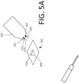
- An example is the DUT substrate 214 shown in FIGs. 2 and 5A -5C.
- the electrical connection point is embedded in or extends from the non-metallic area.
- the dispensed UV-cure conductive adhesive is bonded to the electrically conductive element, the electrical connection point of the DUT, and the non-metallic area of the DUT by applying UV-light from a UV-light source to the dispensed UV-cure conductive adhesive.
- Conventional solder by contrast, sticks only to certain metallic surfaces. Bonding the dispensed UV-cure conductive adhesive to the non-metallic area of the DUT helps to reduce the risk of pulling the electrical connection point off of the DUT, such as the pads, traces, and legs of a printed circuit board assembly.
- the UV-light source may be, as examples, a hand-held, battery-powered, light-emitting diode (LED), such as a consumer-grade UV penlight, or a laboratory-grade UV spot lamp.
- the UV-light may have a wavelength between about 365 nanometers and about 460 nanometers, and the UV-light from the UV-light source may be applied to the dispensed UV-cure conductive adhesive for a duration of between about twenty-five seconds and about thirty-five seconds.
- An operator may determine if the UV-light has been applied for a sufficient period by, for example, visually inspecting the dispensed UV-cure conductive adhesive.
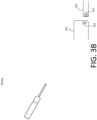
- FIGs. 3A and 3B show an example process of applying pressure during the operation of curing the UV-cure conductive adhesive.
- FIG. 3B diagrammatically shows the topside of the DUT 202 and the underside of the probe tip 205 (where "topside” and “underside” are with reference to FIG. 3A), indicating representative locations of test points 204 on the DUT 202 and the corresponding points 207 on the underside of the probe tip 205.
- Each test point 204 of the DUT 202 and each test point 207 of the probe tip 205 may be a pad, via, trace, pin, connector contact, wire, or other conductive electrical contact point.
- test point 204 of the DUT 202 may be embedded in, or may extend from, a non-metallic area of the DUT 202.
- test point 207 of the probe tip 205 may be embedded in, or may extend from, a non-metallic area of the probe tip 205.
- an applicator 209 may include a UV light source 206 and a cone tip 210.
- the UV light source 206 may shine UV light through the cone tip 210, and the cone tip 210 may contact the probe tip 205 while the UV-cure conductive adhesive is being compressed between the probe tip 205 and the DUT 202.
- the cone tip 210 is formed from a material that will transmit the UV light.
- the cone tip 210 may be made from, for example, fluorinated ethylene propylene, such as the product provided under the name TEFLON ® FEP by The Chemours Company FC, LLC, or PTFE provided under the name TEFLON ® by The Chemours Company FC, LLC.
- the probe tip 205 may be made from a clear or translucent material to allow UV light from the UV light source 206 to pass through the probe tip 205 and illuminate the test points 204 of the DUT 202 and the test points 207 of the probe tip 205.
- the applicator 209 may apply UV light to cure the UV-cure conductive adhesive while also providing pressure through physical contact of the cone tip 210 to the probe tip 205 while the test points 204 of the DUT 202 and the test points 207 of the probe tip 205 are in the curing adhesive.
- FIG. 3A shows the UV-cure conductive adhesive as being applied to the test points 204 of the DUT 202 and the test points 207 of the probe tip 205 by a syringe 208, although the UV-cure conductive adhesive may be applied in any suitable fashion.
- the implementation shown in FIGs. 3A and 3B is especially useful for embodiments in which the UV-cure conductive adhesive is a z-axis-conducting UV material.
- the test points on the DUT and the corresponding points on the underside of the probe tip may be next to or nearby other, undesired points.
- the z-axis-conducting UV material only allows conduction to occur on one axis-the axis between the test points on the DUT and the corresponding points on the probe tip-thus reducing or preventing shorts to adjacent, undesired points.
- the operation of bonding the dispensed UV-cure conductive adhesive may also include applying 105 heat from a heat source to the dispensed UV-cure conductive adhesive.
- the heat is applied after the operation of applying 103 UV-light from the UV-light source to the dispensed UV-cure conductive adhesive.
- the heat source 213 may be, for example, a conventional craft or hobby heat gun.
- the heat may have a temperature less than about 200 degrees Celsius (about 390 degrees Fahrenheit), and the heat may be applied to the dispensed UV-cure conductive adhesive for a duration of between about twenty-five seconds and about thirty-five seconds.
- the heat is applied to raise the temperature of the dispensed UV-cure conductive adhesive to about 100 degrees Celsius (about 210 degrees Fahrenheit) for about thirty seconds. Temperatures greater than about 200 degrees Celsius (about 390 degrees Fahrenheit) may thermally degrade DUTs having conventional substrates, such as FR4 substrates, if the heat is applied for periods of time that are substantially longer than the typical cure times of about sixty seconds or less.
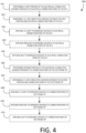
- FIG. 4 is a flowchart showing a method for using a UV-cure conductive adhesive, according to embodiments of the disclosed technology.
- a method 400 for bonding an electrically conductive element between an electrical connection point of a test probe tip and an electrical connection point of a device under test (DUT) may include positioning 401 a first portion of the electrically conductive element proximate to the electrical connection point of the DUT; dispensing 402 a first quantity of UV-cure conductive adhesive between the first portion of the electrically conductive element and the electrical connection point of the DUT; bonding the first quantity of dispensed UV-cure conductive adhesive to the first portion of the electrically conductive element and the electrical connection point of the DUT by applying 403 UV-light from a UV-light source to the first quantity of dispensed UV-cure conductive adhesive; positioning 406 a second portion of the electrically conductive element proximate to the electrical connection point of the test probe tip; dispensing 407 a second quantity
- the first quantity of UV-cure conductive adhesive and the second quantity of UV-cure conductive adhesive may be the same amount of UV-cure conductive adhesive, or they may be different amounts.
- the operation of bonding the first quantity of dispensed UV-cure conductive adhesive to the first portion of the electrically conductive element may also include applying 404 pressure to the first portion of the electrically conductive element and the electrical connection point of the DUT to compress the first quantity of dispensed UV-cure conductive adhesive during the operation of applying 403 UV-light from the UV-light source.
- the operation of bonding the second quantity of dispensed UV-cure conductive adhesive to the second portion of the electrically conductive element may also include applying 409 pressure to the second portion of the electrically conductive element and the electrical connection point of the DUT to compress the second quantity of dispensed UV-cure conductive adhesive during the operation of applying 408 UV-light from the UV-light source.
- the operation of bonding the first quantity of dispensed UV-cure conductive adhesive to the first portion of the electrically conductive element may also include applying 405 heat from a heat source to the first quantity of dispensed UV-cure conductive adhesive.
- the operation of bonding the second quantity of dispensed UV-cure conductive adhesive to the second portion of the electrically conductive element may also include applying 410 heat from a heat source to the second quantity of dispensed UV-cure conductive adhesive.
- the processes and materials in the method 400 of FIG. 4 are as described above for the similar processes and materials in the method 100 of FIG. 1 , including the setups and options shown and described for FIGs. 2 and 4 .
- the first portion of the electrically conductive element may be, for example, a first end of a conductive wire.
- the second portion of the electrically conductive element may be, for example, a second end of the conductive wire, which is opposite the first end of the conductive wire.
- positioning a second portion of the electrically conductive element proximate to the electrical connection point of the test probe tip means positioning the second portion of the electrically conductive element so that the UV-cure conductive adhesive may create an electrical connection between the second portion of the electrically conductive element and the electrical connection point of the test probe tip.
- the second portion of the electrically conductive element may be touching the electrical connection point of the test probe tip.
- the second portion of the electrically conductive element may be sufficiently close to the electrical connection point of the test probe tip so that the UV-cure conductive adhesive may electrically and structurally bridge the distance between the second portion of the electrically conductive element and the electrical connection point of the test probe tip.
- an operator may, for example, perform an electrical continuity test between the second portion of the electrically conductive element and the electrical connection point of the test probe tip once the UV-cure conductive adhesive is cured.
- the dispensed UV-cure conductive adhesive preferably may be bonded to the electrically conductive element and the electrical connection point of the DUT or the test probe tip, as applicable, by (a) applying UV-light from the UV-light source to the dispensed UV-cure conductive adhesive without applying heat or pressure; (b) applying UV-light from the UV-light source and then heat from the heat source to the dispensed UV-cure conductive adhesive without applying pressure; or (c) applying UV-light from the UV-light source and simultaneously applying pressure to the dispensed UV-cure conductive adhesive without applying heat.
- a proximal end 212 of the input wire or probe tip 205 may be bonded to the test probe 201 through the test points 207 of the test probe 201.
- FIG. 5 shows the UV-cure conductive adhesive as being applied by a syringe 208
- the UV-cure conductive adhesive may be applied in any suitable fashion.
- the UV-cure conductive adhesive preferably is an acrylic-based UV-cure conductive adhesive.
- the acrylic-based UV-cure conductive adhesive is a free radical UV reactive acrylate that incorporates an electrically conductive particulate that also has ancillary thermal conductive capabilities.
- the wires or probe tips 205 are integrated into and manufactured as part of the test probe 201, such as in the test probe 201 shown in FIG. 2 .
- the wires or probe tips 205 may be manufactured to a consistent and known length, allowing calibration to be performed on the test probe 201 all the way down to the distal end 211 of the probe tip 205 at the time of manufacture. With this extent of calibration, DSP techniques may be used to correct and remove electrical loading effects of the test probe 201 on the DUT, and provide a user with a more accurate measurement of the signal being measured.
- test probe 201 includes a resistive or impedance element as close as possible to the electrical connection point 104, 204 on the DUT.
- the test probe 201 illustrated in FIG. 2 includes a small conventional resistor at the distal end of probe tips 205.
- the UV-cure conductive adhesive is a resistive formulation. That is, in some embodiments, the UV-cure conductive adhesive is only partially conductive, and presents a resistance or impedance when measured across a dispensed quantity of the adhesive.
- Such a resistive formulation may contain, for example, a mix of silver and carbon as the conductive filler element, the relative proportions of these materials controlling the amount of resistance per unit volume of the adhesive.
- the conventional resistor at the distal end of probe tips 205 may be eliminated, and the dispensed UV-cure conductive adhesive itself functions as the resistive element of the test probe 201, thereby further improving the electrical performance of the test probe 201, since the UV-cure conductive adhesive is directly touching the electrical connection point 104, 204 on the DUT.
- An embodiment of the technologies may include one or more, and any combination of, the examples described below.
- Example 1 includes a method of conductively bonding a test probe tip having an electrically conductive element to a device under test (DUT) having an electrical connection point, the method comprising: positioning the electrically conductive element of the test probe tip proximate to the electrical connection point of the DUT; dispensing a UV-cure conductive adhesive between the electrically conductive element and the electrical connection point of the DUT, the dispensed UV-cure conductive adhesive continuously covering at least a portion of the electrically conductive element and at least a portion of the electrical connection point of the DUT; and bonding the dispensed UV-cure conductive adhesive to the electrically conductive element and the electrical connection point of the DUT by applying UV-light from a UV-light source to the dispensed UV-cure conductive adhesive.
- DUT device under test
- Example 2 includes the method of Example 1, in which the operation of applying UV-light from a UV-light source to the dispensed UV-cure conductive adhesive comprises applying UV-light from a UV-light source to the dispensed UV-cure conductive adhesive for a duration of between about twenty-five seconds and about thirty-five seconds, the UV-light having a wavelength between about 365 nanometers and about 460 nanometers.
- Example 3 includes the method of any of Examples 1-2, the operation of bonding the dispensed UV-cure conductive adhesive further comprising applying heat from a heat source to the dispensed UV-cure conductive adhesive.
- Example 4 includes the method of Example 3, in which the operation of applying heat from a heat source to the dispensed UV-cure conductive adhesive comprises applying heat from a heat source to the dispensed UV-cure conductive adhesive for a duration of between about twenty-five seconds and about thirty-five seconds, the heat having a temperature less than about 200 degrees Celsius.
- Example 5 includes the method of any of Examples 1-4, further comprising applying pressure to the electrically conductive element and the electrical connection point of the DUT to compress the dispensed UV-cure conductive adhesive during the operation of applying UV-light from the UV-light source.
- Example 6 includes the method of any of Examples 1-5, in which the operation of dispensing a UV-cure conductive adhesive between the electrically conductive element and the electrical connection point of the DUT is: dispensing a z-axis-conducting UV-cure adhesive between the electrically conductive element and the electrical connection point of the DUT.
- Example 7 includes the method of any of Examples 1-6, in which the operation of dispensing a UV-cure conductive adhesive between the electrically conductive element and the electrical connection point of the DUT is: dispensing a UV-cure conductive adhesive between the electrically conductive element and the electrical connection point of the DUT, the UV-cure conductive adhesive having a viscosity between about 50,000 centipoise and about 75,000 centipoise.
- Example 9 includes the method of any of Examples 1-8, in which the operation of dispensing a UV-cure conductive adhesive between the electrically conductive element and the electrical connection point of the DUT is: dispensing an acrylic-based UV-cure conductive adhesive between the electrically conductive element and the electrical connection point of the DUT.
- Example 10 includes a test probe tip, having an electrically conductive element, conductively bonded to a device under test (DUT), having an electrical connection point, by a process comprising: positioning the electrically conductive element of the test probe tip proximate to the electrical connection point of the DUT; dispensing a UV-cure conductive adhesive between the electrically conductive element and the electrical connection point of the DUT, the dispensed UV-cure conductive adhesive continuously covering at least a portion of the electrically conductive element and at least a portion of the electrical connection point of the DUT; and bonding the dispensed UV-cure conductive adhesive to the electrically conductive element and the electrical connection point of the DUT by applying UV-light from a UV-light source to the dispensed UV-cure conductive adhesive.
- DUT device under test
- Example 11 includes the test probe tip bonded to a DUT of Example 10, in which the operation of dispensing a UV-cure conductive adhesive between the electrically conductive element and the electrical connection point of the DUT comprises: dispensing a z-axis-conducting UV-cure adhesive between the electrically conductive element and the electrical connection point of the DUT.
- Example 12 includes the test probe tip bonded to a DUT of any of Examples 10-11, in which the operation of dispensing a UV-cure conductive adhesive between the electrically conductive element and the electrical connection point of the DUT comprises: dispensing an acrylic-based UV-cure conductive adhesive between the electrically conductive element and the electrical connection point of the DUT.
- Example 13 includes the test probe tip bonded to a DUT of any of Examples 10-12, in which the dispensed UV-cure conductive adhesive is also continuously covering at least a portion of a non-metallic area of the DUT, and in which the operation of bonding the dispensed UV-cure conductive adhesive to the electrically conductive element and the electrical connection point of the DUT by applying UV-light from a UV-light source to the dispensed UV-cure conductive adhesive is: bonding the dispensed UV-cure conductive adhesive to the electrically conductive element, the electrical connection point of the DUT, and the non-metallic area of the DUT by applying UV-light from a UV-light source to the dispensed UV-cure conductive adhesive.
- Example 14 includes the test probe tip bonded to a DUT of any of Examples 10-13, the process further comprising applying pressure to the electrically conductive element and the electrical connection point of the DUT to compress the dispensed UV-cure conductive adhesive during the operation of applying UV-light from the UV-light source.
- Example 15 includes the test probe tip bonded to a DUT of any of Examples 10-14, in which the operation of dispensing a UV-cure conductive adhesive between the electrically conductive element and the electrical connection point of the DUT comprises: dispensing a UV-cure conductive adhesive between the electrically conductive element and the electrical connection point of the DUT, the UV-cure conductive adhesive having a viscosity between about 50,000 centipoise and about 75,000 centipoise.
- Example 16 includes a method of conductively bonding a test probe tip to a device under test (DUT), the method comprising: positioning a first portion of an electrically conductive element proximate to an electrical connection point of the DUT; dispensing a first quantity of UV-cure conductive adhesive between the first portion of the electrically conductive element and the electrical connection point of the DUT, the dispensed first quantity of UV-cure conductive adhesive continuously covering at least a portion of the first portion of the electrically conductive element and at least a portion of the electrical connection point of the DUT; bonding the dispensed first quantity of UV-cure conductive adhesive to the first portion of the electrically conductive element and the electrical connection point of the DUT by applying UV-light from a UV-light source to the dispensed first quantity of UV-cure conductive adhesive; positioning a second portion of an electrically conductive element proximate to an electrical connection point of the test probe tip; dispensing a second quantity of UV-cure conductive adhesive between the second
- Example 17 includes the method of Example 16, in which the operation of applying UV-light from a UV-light source to the dispensed first quantity of UV-cure conductive adhesive comprises applying UV-light from a UV-light source to the dispensed first quantity of UV-cure conductive adhesive for a duration of between about twenty-five seconds and about thirty-five seconds, the UV-light having a wavelength between about 365 nanometers and about 460 nanometers.
- Example 19 includes the method of any of Examples 16-18, the operation of bonding the dispensed first quantity of UV-cure conductive adhesive further comprising applying heat from a heat source to the dispensed first quantity of UV-cure conductive adhesive.
- Example 20 includes the method of Example 19, in which the operation of applying heat from a heat source to the first quantity of dispensed UV-cure conductive adhesive comprises applying heat from a heat source to the dispensed first quantity of UV-cure conductive adhesive for a duration of between about twenty-five seconds and about thirty-five seconds, the heat having a temperature less than about 200 degrees Celsius.
- Example 21 includes the method of any of Examples 16-20, the operation of bonding the dispensed second quantity of UV-cure conductive adhesive further comprising applying heat from a heat source to the dispensed second quantity of UV-cure conductive adhesive.
- Example 22 includes the method of Example 21, in which the operation of applying heat from a heat source to the second quantity of dispensed UV-cure conductive adhesive comprises applying heat from a heat source to the dispensed second quantity of UV-cure conductive adhesive for a duration of between about twenty-five seconds and about thirty-five seconds, the heat having a temperature less than about 200 degrees Celsius.
- Example 23 includes the method of any of Examples 16-22, further comprising applying pressure to the first portion of the electrically conductive element and the electrical connection point of the DUT to compress the dispensed first quantity of UV-cure conductive adhesive during the operation of applying UV-light from the UV-light source.
- Example 25 includes the method of any of Examples 16-24, in which the operation of dispensing a first quantity of UV-cure conductive adhesive between the first portion of the electrically conductive element and the electrical connection point of the DUT is: dispensing a first quantity of z-axis-conducting UV-cure adhesive between the first portion of the electrically conductive element and the electrical connection point of the DUT.
- Example 26 includes the method of any of Examples 16-25, in which the operation of dispensing a second quantity of UV-cure conductive adhesive between the second portion of the electrically conductive element and the electrical connection point of the test probe tip is: dispensing a second quantity of z-axis-conducting UV-cure adhesive between the second portion of the electrically conductive element and the electrical connection point of the test probe tip.
- Example 27 includes the method of any of Examples 16-26, in which the operation of dispensing a first quantity of UV-cure conductive adhesive between the first portion of the electrically conductive element and the electrical connection point of the DUT is: dispensing a first quantity of UV-cure conductive adhesive between the first portion of the electrically conductive element and the electrical connection point of the DUT, the first quantity of UV-cure conductive adhesive having a viscosity between about 50,000 centipoise and about 75,000 centipoise.
- Example 28 includes the method of any of Examples 16-27, in which the operation of dispensing a second quantity of UV-cure conductive adhesive between the second portion of the electrically conductive element and the electrical connection point of the test probe tip is: dispensing a second quantity of UV-cure conductive adhesive between the second portion of the electrically conductive element and the electrical connection point of the test probe tip, the second quantity of UV-cure conductive adhesive having a viscosity between about 50,000 centipoise and about 75,000 centipoise.
- Example 29 includes the method of any of Examples 16-28, in which the dispensed first quantity of UV-cure conductive adhesive is also continuously covering at least a portion of a non-metallic area of the DUT, and in which the operation of bonding the dispensed first quantity of UV-cure conductive adhesive to the first portion of the electrically conductive element and the electrical connection point of the DUT by applying UV-light from a UV-light source to the dispensed first quantity of UV-cure conductive adhesive is: bonding the dispensed first quantity of UV-cure conductive adhesive to the first portion of the electrically conductive element, the electrical connection point of the DUT, and the non-metallic area of the DUT by applying UV-light from a UV-light source to the dispensed first quantity of UV-cure conductive adhesive.
- Example 30 includes the method of any of Examples 16-29, in which the dispensed second quantity of UV-cure conductive adhesive is also continuously covering at least a portion of a non-metallic area of the test probe tip, and in which the operation of bonding the dispensed second quantity of UV-cure conductive adhesive to the second portion of the electrically conductive element and the electrical connection point of the test probe tip by applying UV-light from a UV-light source to the dispensed second quantity of UV-cure conductive adhesive is: bonding the dispensed second quantity of UV-cure conductive adhesive to the second portion of the electrically conductive element, the electrical connection point of the test probe tip, and the non-metallic area of the test probe tip by applying UV-light from a UV-light source to the dispensed second quantity of UV-cure conductive adhesive.
- Example 31 includes the method of any of Examples 16-30, in which the operation of dispensing a first quantity of UV-cure conductive adhesive between the first portion of the electrically conductive element and the electrical connection point of the DUT is: dispensing a first quantity of acrylic-based UV-cure conductive adhesive between the first portion of the electrically conductive element and the electrical connection point of the DUT.
- Example 32 includes the method of any of Examples 16-31, in which the operation of dispensing a second quantity of UV-cure conductive adhesive between the second portion of the electrically conductive element and the electrical connection point of the test probe tip is: dispensing a second quantity of acrylic-based UV-cure conductive adhesive between the second portion of the electrically conductive element and the electrical connection point of the test probe tip.
- Example 33 includes a test system comprising: a test and measurement instrument; and a test probe tip, having an electrically conductive element, conductively bonded to a device under test (DUT), having an electrical connection point, by a process comprising: positioning the electrically conductive element of the test probe tip proximate to the electrical connection point of the DUT; dispensing a UV-cure conductive adhesive between the electrically conductive element and the electrical connection point of the DUT, the dispensed UV-cure conductive adhesive continuously covering at least a portion of the electrically conductive element and at least a portion of the electrical connection point of the DUT; and bonding the dispensed UV-cure conductive adhesive to the electrically conductive element and the electrical connection point of the DUT by applying UV-light from a UV-light source to the dispensed UV-cure conductive adhesive.
- a test system comprising: a test and measurement instrument; and a test probe tip, having an electrically conductive element, conductively bonded to a device
- Example 34 includes the test system of Example 33, in which the test and measurement instrument is an oscilloscope.
- an article “comprising” or “which comprises” components A, B, and C can contain only components A, B, and C, or it can contain components A, B, and C along with one or more other components.
Landscapes
- Physics & Mathematics (AREA)
- General Physics & Mathematics (AREA)
- Engineering & Computer Science (AREA)
- Manufacturing & Machinery (AREA)
- Microelectronics & Electronic Packaging (AREA)
- Chemical & Material Sciences (AREA)
- Organic Chemistry (AREA)
- Connections Effected By Soldering, Adhesion, Or Permanent Deformation (AREA)
- Measuring Leads Or Probes (AREA)
- Tests Of Electronic Circuits (AREA)
- Adhesives Or Adhesive Processes (AREA)
- Testing Or Measuring Of Semiconductors Or The Like (AREA)
Claims (15)
- (100) Procédé de liaison conductrice d'une pointe (205) de sonde de test (201) ayant un élément électriquement conducteur à un dispositif sous test, DUT, (202) ayant un point de connexion électrique, le procédé comprenant :le positionnement (101) de l'élément électriquement conducteur de la pointe (205) de sonde de test (201) à proximité du point de connexion électrique du DUT (202) ;la distribution (102) d'un adhésif conducteur à durcissement UV (203) entre l'élément électriquement conducteur et le point de connexion électrique du DUT (202), l'adhésif conducteur à durcissement UV (203) distribué recouvrant en continu au moins une partie de l'élément électriquement conducteur et au moins une partie du point de connexion électrique du DUT (202) ; etla liaison de l'adhésif conducteur à durcissement UV (203) distribué à l'élément électriquement conducteur et au point de connexion électrique du DUT (202) par l'application (103) de lumière UV provenant d'une source de lumière UV à l'adhésif conducteur à durcissement UV (203) distribué.
- Procédé (100) selon la revendication 1, dans lequel l'opération d'application (103) de lumière UV provenant d'une source de lumière UV (206) à l'adhésif conducteur à durcissement UV (203) distribué comprend l'application (103) de lumière UV provenant d'une source de lumière UV (206) sur l'adhésif conducteur à durcissement UV (203) distribué pendant une durée comprise entre environ vingt-cinq secondes et environ trente-cinq secondes, la lumière UV ayant une longueur d'onde comprise entre environ 365 nanomètres et environ 460 nanomètres.
- Procédé (100) selon la revendication 1 ou 2, l'opération de liaison de l'adhésif conducteur à durcissement UV (203) distribué comprenant en outre l'application de chaleur (105) provenant d'une source de chaleur (213) à l'adhésif conducteur à durcissement UV (203) distribué ; et éventuellement
dans lequel l'opération d'application de chaleur (105) provenant d'une source de chaleur (213) à l'adhésif conducteur à durcissement UV (203) distribué comprend l'application de chaleur (105) provenant d'une source de chaleur (213) à l'adhésif conducteur à durcissement UV (203) distribué pendant une durée comprise entre environ vingt-cinq secondes et environ trente-cinq secondes, la chaleur ayant une température inférieure à environ 200 degrés Celsius. - Procédé (100) selon l'une quelconque des revendications 1 à 3, comprenant en outre l'application d'une pression (104) à l'élément électriquement conducteur et au point de connexion électrique du DUT (202) pour comprimer l'adhésif conducteur à durcissement UV (203) distribué pendant l'opération d'application de lumière UV provenant de la source de lumière UV (206).
- Procédé (100) selon l'une quelconque des revendications 1 à 4, dans lequel l'opération de distribution (102) d'un adhésif conducteur à durcissement UV (203) entre l'élément électriquement conducteur et le point de connexion électrique du DUT (202) est :la distribution d'un adhésif à durcissement UV conducteur d'axe z (203) entre l'élément électriquement conducteur et le point de connexion électrique du DUT (202) ; et/oula distribution d'un adhésif conducteur à durcissement UV (203) entre l'élément électriquement conducteur et le point de connexion électrique du DUT (202), l'adhésif conducteur à durcissement UV (203) ayant une viscosité comprise entre environ 50 000 centipoises et environ 75 000 centipoises.
- Procédé (100) selon l'une quelconque des revendications 1 à 5, dans lequel l'adhésif conducteur à durcissement UV (203) distribué recouvre également en continu au moins une partie d'une zone non métallique du DUT (202), et dans lequel l'opération de liaison de l'adhésif conducteur à durcissement UV (203) distribué à l'élément électriquement conducteur et au point de connexion électrique du DUT (202) par l'application de lumière UV provenant d'une source de lumière UV (206) à l'adhésif conducteur à durcissement UV (203) distribué est :
la liaison de l'adhésif conducteur à durcissement UV (203) distribué à l'élément électriquement conducteur, au point de connexion électrique du DUT (202) et à la zone non métallique du DUT (202) par l'application (103) de lumière UV provenant d'une source de lumière UV (206) à l'adhésif conducteur à durcissement UV (203) distribué. - Procédé (100) selon l'une quelconque des revendications 1 à 6, dans lequel l'opération de distribution (102) d'un adhésif conducteur à durcissement UV (203) entre l'élément électriquement conducteur et le point de connexion électrique du DUT (202) est :
la distribution d'un adhésif conducteur à durcissement UV (203) à base d'acrylique entre l'élément électriquement conducteur et le point de connexion électrique du DUT (202). - Pointe (205) de sonde de test (201), ayant un élément électriquement conducteur, lié de manière conductrice à un dispositif sous test, DUT, (202) ayant un point de connexion électrique, par un processus comprenant :le positionnement (101) de l'élément électriquement conducteur de la pointe (205) de sonde de test (201) à proximité du point de connexion électrique du DUT (202) ;la distribution (102) d'un adhésif conducteur à durcissement UV (203) entre l'élément électriquement conducteur et le point de connexion électrique du DUT (202), l'adhésif conducteur à durcissement UV (203) distribué recouvrant en continu au moins une partie de l'élément électriquement conducteur et au moins une partie du point de connexion électrique du DUT (202) ; etla liaison de l'adhésif conducteur à durcissement UV (203) distribué à l'élément électriquement conducteur et au point de connexion électrique du DUT (202) par l'application (103) de lumière UV provenant d'une source de lumière UV (206) à l'adhésif conducteur à durcissement UV (203) distribué.
- Pointe (205) de sonde de test (201) liée à un DUT (202) selon la revendication 8, dans laquelle l'opération de distribution (102) d'un adhésif conducteur à durcissement UV (203) entre l'élément électriquement conducteur et le point de connexion électrique du DUT (202) comprend :la distribution d'un adhésif à durcissement UV conducteur d'axe z (203) entre l'élément électriquement conducteur et le point de connexion électrique du DUT (202) ; et/oula distribution d'un adhésif conducteur à durcissement UV (203) à base d'acrylique entre l'élément électriquement conducteur et le point de connexion électrique du DUT (202).
- Pointe (205) de sonde de test (201) liée à un DUT 202) selon la revendication 8 ou 9, dans laquelle l'adhésif conducteur à durcissement UV (203) distribué recouvre également en continu au moins une partie d'une zone non métallique du DUT (202), et dans laquelle l'opération de liaison de l'adhésif conducteur à durcissement UV (203) distribué à l'élément électriquement conducteur et au point de connexion électrique du DUT (202) par l' application de lumière UV provenant d'une source de lumière UV (206) à l'adhésif conducteur à durcissement UV (203) distribué est :
la liaison de l'adhésif conducteur à durcissement UV (203) distribué à l'élément électriquement conducteur, au point de connexion électrique du DUT (202) et à la zone non métallique du DUT (202) par l'application (103) de lumière UV provenant d'une source de lumière UV (206) à l'adhésif conducteur à durcissement UV (203) distribué. - Pointe (205) de sonde de test (201) liée à un DUT (202) selon l'une quelconque des revendications 8 à 10, le processus comprenant en outre l'application de pression (104) à l'élément électriquement conducteur et au point de connexion électrique du DUT (202) pour comprimer l'adhésif conducteur à durcissement UV (203) distribué pendant l'opération d'application de lumière UV provenant de la source de lumière UV (206).
- Procédé (400) de liaison conductrice d'une pointe (205) de sonde de test (201) ayant un élément électriquement conducteur avec deux parties à un dispositif sous test, DUT, (202), le procédé comprenant :le positionnement (401) d'une première partie (211) d'un élément électriquement conducteur à proximité d'un point de connexion électrique du DUT (202) ;la distribution (402) d'une première quantité d'adhésif conducteur à durcissement UV (203) entre la première partie (211) de l'élément électriquement conducteur et le point de connexion électrique du DUT (202), la première quantité distribuée d'adhésif conducteur à durcissement UV (203) recouvrant en continu au moins une partie de la première partie (211) de l'élément électriquement conducteur et au moins une partie du point de connexion électrique du DUT (202) ;la liaison de la première quantité distribuée d'adhésif conducteur à durcissement UV à la première partie (211) de l'élément électriquement conducteur et au point de connexion électrique du DUT (202) par l'application (403) de lumière UV provenant d'une source de lumière UV (206) à la première quantité distribuée d'adhésif conducteur à durcissement UV (203) ;le positionnement (406) d'une seconde partie (212) d'un élément électriquement conducteur à proximité d'un point de connexion électrique de la pointe (205) de sonde de test (201) ;la distribution (407) d'une seconde quantité d'adhésif conducteur à durcissement UV (203) entre la seconde partie (212) de l'élément électriquement conducteur et le point de connexion électrique de la pointe (205) de sonde de test (201), la seconde quantité distribuée d'adhésif conducteur à durcissement UV (203) recouvrant en continu au moins une partie de la seconde partie (212) de l'élément électriquement conducteur et au moins une partie du point de connexion électrique de la pointe (205) de sonde de test (201) ; etla liaison de la seconde quantité distribuée d'adhésif conducteur à durcissement UV à la seconde partie (212) de l'élément électriquement conducteur et au point de connexion électrique de la pointe de sonde de test par l'application (408) de lumière UV provenant de la source de lumière UV (206) à la seconde quantité distribuée d'adhésif conducteur à durcissement UV (203).
- Procédé selon la revendication 12, dans lequel une ou plusieurs de la première ou de la seconde quantité distribuée d'adhésif conducteur à durcissement UV (203) recouvre également en continu au moins une partie d'une zone non métallique du DUT (202), et dans lequel l'opération de liaison de la première ou la seconde quantité distribuée d'adhésif conducteur à durcissement UV (203) à la première (211) ou la seconde (212) partie respective de l'élément électriquement conducteur et au point de connexion électrique du DUT (202) par l'application (403,408) de lumière UV provenant d'une source de lumière UV (206) à la première ou la seconde quantité distribuée d'adhésif conducteur à durcissement UV (203) est :
la liaison de la première ou la seconde quantité distribuée d'adhésif conducteur à durcissement UV (203) à la première (211) ou la seconde (212) partie respective de l'élément électriquement conducteur, au point de connexion électrique du DUT (202) et à la zone non métallique du DUT (202) par l'application de lumière UV provenant d'une source de lumière UV (206) à la première ou la seconde quantité distribuée d'adhésif conducteur à durcissement UV (203). - Système de test comprenant :un instrument de test et de mesure ; etla pointe de sonde de test selon l'une quelconque des revendications 8 à 11.
- Système de test selon la revendication 14, dans lequel l'instrument de test et de mesure est un oscilloscope.
Applications Claiming Priority (3)
| Application Number | Priority Date | Filing Date | Title |
|---|---|---|---|
| US201762511454P | 2017-05-26 | 2017-05-26 | |
| US201862635526P | 2018-02-26 | 2018-02-26 | |
| US15/978,090 US10739381B2 (en) | 2017-05-26 | 2018-05-11 | Component attachment technique using a UV-cure conductive adhesive |
Publications (3)
| Publication Number | Publication Date |
|---|---|
| EP3413060A1 EP3413060A1 (fr) | 2018-12-12 |
| EP3413060B1 true EP3413060B1 (fr) | 2023-07-05 |
| EP3413060C0 EP3413060C0 (fr) | 2023-07-05 |
Family
ID=62386171
Family Applications (1)
| Application Number | Title | Priority Date | Filing Date |
|---|---|---|---|
| EP18174427.7A Active EP3413060B1 (fr) | 2017-05-26 | 2018-05-25 | Technique de fixation de composants à l'aide d'un adhésif conducteur de durcissement par uv |
Country Status (4)
| Country | Link |
|---|---|
| US (1) | US10739381B2 (fr) |
| EP (1) | EP3413060B1 (fr) |
| JP (1) | JP7420467B2 (fr) |
| CN (1) | CN108929638B (fr) |
Families Citing this family (4)
| Publication number | Priority date | Publication date | Assignee | Title |
|---|---|---|---|---|
| JP6609073B1 (ja) * | 2019-01-15 | 2019-11-20 | 株式会社日本マイクロニクス | プローブ基板及び電気的接続装置 |
| EP3787013A1 (fr) * | 2019-08-27 | 2021-03-03 | Heraeus Deutschland GmbH & Co KG | Procede de connexion d'un article electroconducteur avec une substance durcissable aux uv, dispositif correspondant et procede d'utilisation |
| JP2021076590A (ja) * | 2019-10-03 | 2021-05-20 | テクトロニクス・インコーポレイテッドTektronix,Inc. | 封止された試験ポイントから信号を取得する方法及び試験測定装置を試験ポイントに電気的に接続するシステム |
| US12055578B2 (en) * | 2020-07-08 | 2024-08-06 | Tektronix, Inc. | Securing a probe to a device under test |
Family Cites Families (40)
| Publication number | Priority date | Publication date | Assignee | Title |
|---|---|---|---|---|
| US4976897A (en) * | 1987-12-16 | 1990-12-11 | Hoechst Celanese Corporation | Composite porous membranes and methods of making the same |
| US4999136A (en) | 1988-08-23 | 1991-03-12 | Westinghouse Electric Corp. | Ultraviolet curable conductive resin |
| DE3923023A1 (de) | 1989-07-12 | 1991-01-24 | Siemens Ag | Uv-haertbarer klebstoff fuer ein halbleiterchipmontageverfahren |
| JP2833875B2 (ja) * | 1991-04-16 | 1998-12-09 | キヤノン株式会社 | インクジェットヘッドの製造方法、及びその製造機 |
| US5820716A (en) | 1993-11-05 | 1998-10-13 | Micron Technology, Inc. | Method for surface mounting electrical components to a substrate |
| JP3505328B2 (ja) * | 1995-12-18 | 2004-03-08 | 松下電器産業株式会社 | 半導体装置およびその製造方法 |
| US6329829B1 (en) | 1997-08-22 | 2001-12-11 | Micron Technology, Inc. | Interconnect and system for making temporary electrical connections to semiconductor components |
| US6043670A (en) * | 1997-12-16 | 2000-03-28 | Lucent Technologies Inc. | Method for testing integrated circuits |
| JP3120796B2 (ja) | 1998-11-17 | 2000-12-25 | 日本電気株式会社 | 電気的検査用コンタクトプローブの製造方法 |
| JP3104703B1 (ja) | 1999-10-26 | 2000-10-30 | 松下電器産業株式会社 | 液晶素子の製造方法 |
| JP2001267372A (ja) | 2000-03-21 | 2001-09-28 | Toshiba Corp | 光電変換装置及びその製造方法と、それを用いたカメラ |
| US20020118032A1 (en) | 2001-02-28 | 2002-08-29 | Schlumberger Technologies, Inc. | Heating apparatus containing an array of surface mount components for DUT performance testing |
| US6528352B1 (en) * | 2001-10-17 | 2003-03-04 | International Business Machines Corporation | Use of conductive adhesive to form temporary electrical connections for use in TCA (temporary chip attach) applications |
| CN1236435C (zh) * | 2002-01-24 | 2006-01-11 | 株式会社三协精机制作所 | 粘接方法和光头装置的制造方法 |
| US6937039B2 (en) * | 2003-05-28 | 2005-08-30 | Hewlett-Packard Development Company, L.P. | Tip and tip assembly for a signal probe |
| DE10343256B4 (de) | 2003-09-17 | 2006-08-10 | Infineon Technologies Ag | Anordnung zur Herstellung einer elektrischen Verbindung zwischen einem BGA-Package und einer Signalquelle, sowie Verfahren zum Herstellen einer solchen Verbindung |
| CN101189524A (zh) | 2005-03-01 | 2008-05-28 | Sv探针私人有限公司 | 具有层叠基板的探针卡 |
| KR100975904B1 (ko) | 2005-06-27 | 2010-08-16 | 가부시키가이샤 아드반테스트 | 콘택터, 그 콘택터를 구비한 콘택트 스트럭처, 프로브카드, 시험 장치, 콘택트 스트럭처 제조방법, 및 콘택트스트럭처 제조장치 |
| JP2007184487A (ja) | 2006-01-10 | 2007-07-19 | Integrated Service Technology Inc | 回路信号の引出方法 |
| US7786740B2 (en) | 2006-10-11 | 2010-08-31 | Astria Semiconductor Holdings, Inc. | Probe cards employing probes having retaining portions for potting in a potting region |
| US8441271B2 (en) * | 2007-04-03 | 2013-05-14 | Advantest Corporation | Contactor and method of production of contactor |
| JP5100751B2 (ja) | 2007-07-03 | 2012-12-19 | 株式会社アドバンテスト | プローブおよびプローブカード |
| JP2011506751A (ja) * | 2007-12-18 | 2011-03-03 | スリーエム イノベイティブ プロパティズ カンパニー | 導電性接着剤前駆体、その使用方法、及び物品 |
| US7692436B2 (en) | 2008-03-20 | 2010-04-06 | Touchdown Technologies, Inc. | Probe card substrate with bonded via |
| JP5585000B2 (ja) | 2009-05-22 | 2014-09-10 | 富士通セミコンダクター株式会社 | 半導体装置 |
| JP5465516B2 (ja) | 2009-12-08 | 2014-04-09 | 日本電子材料株式会社 | プローブ及びプローブの製造方法 |
| JP2012102317A (ja) * | 2010-10-13 | 2012-05-31 | Sony Chemical & Information Device Corp | アクリル系粘着テープ及びその製造方法 |
| US8884640B2 (en) | 2011-04-28 | 2014-11-11 | Mpi Corporation | Integrated high-speed probe system |
| US9605940B2 (en) | 2011-05-25 | 2017-03-28 | Helmut Fischer GbmH Institut für Elektronik und Messtechnik | Measuring probe for measuring the thickness of thin layers, and method for the production of a sensor element for the measuring probe |
| US20120319710A1 (en) | 2011-06-15 | 2012-12-20 | Probelogic, Inc. | Method and apparatus for implementing probes for electronic circuit testing |
| US9285419B2 (en) | 2011-06-30 | 2016-03-15 | Apple Inc. | Test probe alignment structures for radio-frequency test systems |
| WO2013039226A1 (fr) * | 2011-09-14 | 2013-03-21 | 電気化学工業株式会社 | Composition, et procédé de fixation temporaire d'éléments mettant en œuvre celle-ci |
| US20140091818A1 (en) | 2012-10-03 | 2014-04-03 | Corad Technology Inc. | Fine pitch interface for probe card |
| US9482695B2 (en) | 2012-12-21 | 2016-11-01 | Tektronix, Inc. | High bandwidth differential lead with device connection |
| US9435856B2 (en) | 2013-04-16 | 2016-09-06 | Mpi Corporation | Position adjustable probing device and probe card assembly using the same |
| JP6259590B2 (ja) | 2013-06-12 | 2018-01-10 | 株式会社日本マイクロニクス | プローブカード及びその製造方法 |
| CN103344791B (zh) | 2013-06-26 | 2016-07-06 | 中国科学院深圳先进技术研究院 | 一种测试基板及采用该测试基板制造的探针卡 |
| KR102123989B1 (ko) * | 2013-12-17 | 2020-06-26 | 삼성전자주식회사 | 테스터 및 이를 구비하는 반도체 소자 검사 장치 |
| EP3095159A4 (fr) | 2014-01-17 | 2017-09-27 | Nuvotronics, Inc. | Unité d'interface de test à l'échelle d'une tranche: dispositifs et procédés à faible perte et haute isolation pour interconnexions de signaux mixtes à grande vitesse et haute densité, et contacteurs |
| JP6425899B2 (ja) * | 2014-03-11 | 2018-11-21 | デクセリアルズ株式会社 | 異方性導電接着剤、接続体の製造方法及び電子部品の接続方法 |
-
2018
- 2018-05-11 US US15/978,090 patent/US10739381B2/en active Active
- 2018-05-25 JP JP2018100925A patent/JP7420467B2/ja active Active
- 2018-05-25 CN CN201810513424.6A patent/CN108929638B/zh active Active
- 2018-05-25 EP EP18174427.7A patent/EP3413060B1/fr active Active
Also Published As
| Publication number | Publication date |
|---|---|
| US10739381B2 (en) | 2020-08-11 |
| EP3413060C0 (fr) | 2023-07-05 |
| CN108929638B (zh) | 2022-11-04 |
| JP7420467B2 (ja) | 2024-01-23 |
| US20180340956A1 (en) | 2018-11-29 |
| CN108929638A (zh) | 2018-12-04 |
| EP3413060A1 (fr) | 2018-12-12 |
| JP2019002916A (ja) | 2019-01-10 |
Similar Documents
| Publication | Publication Date | Title |
|---|---|---|
| US10739381B2 (en) | Component attachment technique using a UV-cure conductive adhesive | |
| US10859598B1 (en) | Back-drilled via attachment technique using a UV-cure conductive adhesive | |
| Gilleo | Assembly with conductive adhesives | |
| US9081037B2 (en) | Attachment of an electrical element to an electronic device using a conductive material | |
| JP5464949B2 (ja) | 保護膜の形成方法および実装構造体、ならびに実装構造体のリペア方法 | |
| US11385258B2 (en) | Encapsulated component attachment technique using a UV-cure conductive adhesive | |
| US11647591B2 (en) | Compliant pin surface mount technology pad for rework | |
| US20200146194A1 (en) | Back-drilled via probing techniques | |
| Kuhn et al. | Test methods and influencing factors for the adhesion strength measurement of metallized structures on thermoplastic substrates | |
| CN112611900A (zh) | 使用uv固化导电粘接剂的包封组件附接技术 | |
| KR200462339Y1 (ko) | 반도체 테스트 설비의 포고 핀 | |
| Fidan et al. | Designed experiments to investigate the solder joint quality output of a prototype automated surface mount replacement system | |
| US8608217B1 (en) | Electronic component grasping tool | |
| US11778753B2 (en) | UV fixing glue for assembly | |
| JP2022016381A (ja) | プローブ・チップ及びその固定方法 | |
| JP2688444B2 (ja) | 半導体lsi検査装置 | |
| Varzaru et al. | A Study of SW150 Conductive Paste as a possible use in Solderless Assembly for Electronics | |
| JP4257782B2 (ja) | 同軸ケーブルの高周波特性測定評価方法 | |
| Stam et al. | Characterisation and reliability study of anisotropic conductive adhesives for fine pitch package assembly | |
| Consiglio et al. | Development of a duothermal soldering process | |
| JP2004235412A (ja) | プリント配線板用基板材料およびプリント配線板の導体密着強度試験方法 | |
| JPH047476B2 (fr) | ||
| WO2016157594A1 (fr) | Matériau d'assemblage sous forme de feuille, composant électronique l'utilisant, procédé d'assemblage, et corps assemblé | |
| JP2023161934A (ja) | コンタクトプローブ | |
| JP2009063469A (ja) | 表面実装部品の信号引き出し治具 |
Legal Events
| Date | Code | Title | Description |
|---|---|---|---|
| PUAI | Public reference made under article 153(3) epc to a published international application that has entered the european phase |
Free format text: ORIGINAL CODE: 0009012 |
|
| STAA | Information on the status of an ep patent application or granted ep patent |
Free format text: STATUS: THE APPLICATION HAS BEEN PUBLISHED |
|
| AK | Designated contracting states |
Kind code of ref document: A1 Designated state(s): AL AT BE BG CH CY CZ DE DK EE ES FI FR GB GR HR HU IE IS IT LI LT LU LV MC MK MT NL NO PL PT RO RS SE SI SK SM TR |
|
| AX | Request for extension of the european patent |
Extension state: BA ME |
|
| STAA | Information on the status of an ep patent application or granted ep patent |
Free format text: STATUS: REQUEST FOR EXAMINATION WAS MADE |
|
| 17P | Request for examination filed |
Effective date: 20190612 |
|
| RBV | Designated contracting states (corrected) |
Designated state(s): AL AT BE BG CH CY CZ DE DK EE ES FI FR GB GR HR HU IE IS IT LI LT LU LV MC MK MT NL NO PL PT RO RS SE SI SK SM TR |
|
| GRAP | Despatch of communication of intention to grant a patent |
Free format text: ORIGINAL CODE: EPIDOSNIGR1 |
|
| STAA | Information on the status of an ep patent application or granted ep patent |
Free format text: STATUS: GRANT OF PATENT IS INTENDED |
|
| INTG | Intention to grant announced |
Effective date: 20220428 |
|
| GRAJ | Information related to disapproval of communication of intention to grant by the applicant or resumption of examination proceedings by the epo deleted |
Free format text: ORIGINAL CODE: EPIDOSDIGR1 |
|
| STAA | Information on the status of an ep patent application or granted ep patent |
Free format text: STATUS: REQUEST FOR EXAMINATION WAS MADE |
|
| GRAP | Despatch of communication of intention to grant a patent |
Free format text: ORIGINAL CODE: EPIDOSNIGR1 |
|
| STAA | Information on the status of an ep patent application or granted ep patent |
Free format text: STATUS: GRANT OF PATENT IS INTENDED |
|
| INTC | Intention to grant announced (deleted) | ||
| INTG | Intention to grant announced |
Effective date: 20220929 |
|
| GRAS | Grant fee paid |
Free format text: ORIGINAL CODE: EPIDOSNIGR3 |
|
| GRAA | (expected) grant |
Free format text: ORIGINAL CODE: 0009210 |
|
| STAA | Information on the status of an ep patent application or granted ep patent |
Free format text: STATUS: THE PATENT HAS BEEN GRANTED |
|
| AK | Designated contracting states |
Kind code of ref document: B1 Designated state(s): AL AT BE BG CH CY CZ DE DK EE ES FI FR GB GR HR HU IE IS IT LI LT LU LV MC MK MT NL NO PL PT RO RS SE SI SK SM TR |
|
| REG | Reference to a national code |
Ref country code: CH Ref legal event code: EP |
|
| REG | Reference to a national code |
Ref country code: AT Ref legal event code: REF Ref document number: 1585317 Country of ref document: AT Kind code of ref document: T Effective date: 20230715 |
|
| REG | Reference to a national code |
Ref country code: DE Ref legal event code: R096 Ref document number: 602018052718 Country of ref document: DE |
|
| REG | Reference to a national code |
Ref country code: IE Ref legal event code: FG4D |
|
| U01 | Request for unitary effect filed |
Effective date: 20230724 |
|
| U07 | Unitary effect registered |
Designated state(s): AT BE BG DE DK EE FI FR IT LT LU LV MT NL PT SE SI Effective date: 20230728 |
|
| REG | Reference to a national code |
Ref country code: LT Ref legal event code: MG9D |
|
| PG25 | Lapsed in a contracting state [announced via postgrant information from national office to epo] |
Ref country code: GR Free format text: LAPSE BECAUSE OF FAILURE TO SUBMIT A TRANSLATION OF THE DESCRIPTION OR TO PAY THE FEE WITHIN THE PRESCRIBED TIME-LIMIT Effective date: 20231006 |
|
| PG25 | Lapsed in a contracting state [announced via postgrant information from national office to epo] |
Ref country code: ES Free format text: LAPSE BECAUSE OF FAILURE TO SUBMIT A TRANSLATION OF THE DESCRIPTION OR TO PAY THE FEE WITHIN THE PRESCRIBED TIME-LIMIT Effective date: 20230705 |
|
| PG25 | Lapsed in a contracting state [announced via postgrant information from national office to epo] |
Ref country code: IS Free format text: LAPSE BECAUSE OF FAILURE TO SUBMIT A TRANSLATION OF THE DESCRIPTION OR TO PAY THE FEE WITHIN THE PRESCRIBED TIME-LIMIT Effective date: 20231105 |
|
| PG25 | Lapsed in a contracting state [announced via postgrant information from national office to epo] |
Ref country code: RS Free format text: LAPSE BECAUSE OF FAILURE TO SUBMIT A TRANSLATION OF THE DESCRIPTION OR TO PAY THE FEE WITHIN THE PRESCRIBED TIME-LIMIT Effective date: 20230705 Ref country code: NO Free format text: LAPSE BECAUSE OF FAILURE TO SUBMIT A TRANSLATION OF THE DESCRIPTION OR TO PAY THE FEE WITHIN THE PRESCRIBED TIME-LIMIT Effective date: 20231005 Ref country code: IS Free format text: LAPSE BECAUSE OF FAILURE TO SUBMIT A TRANSLATION OF THE DESCRIPTION OR TO PAY THE FEE WITHIN THE PRESCRIBED TIME-LIMIT Effective date: 20231105 Ref country code: HR Free format text: LAPSE BECAUSE OF FAILURE TO SUBMIT A TRANSLATION OF THE DESCRIPTION OR TO PAY THE FEE WITHIN THE PRESCRIBED TIME-LIMIT Effective date: 20230705 Ref country code: GR Free format text: LAPSE BECAUSE OF FAILURE TO SUBMIT A TRANSLATION OF THE DESCRIPTION OR TO PAY THE FEE WITHIN THE PRESCRIBED TIME-LIMIT Effective date: 20231006 Ref country code: ES Free format text: LAPSE BECAUSE OF FAILURE TO SUBMIT A TRANSLATION OF THE DESCRIPTION OR TO PAY THE FEE WITHIN THE PRESCRIBED TIME-LIMIT Effective date: 20230705 |
|
| PG25 | Lapsed in a contracting state [announced via postgrant information from national office to epo] |
Ref country code: PL Free format text: LAPSE BECAUSE OF FAILURE TO SUBMIT A TRANSLATION OF THE DESCRIPTION OR TO PAY THE FEE WITHIN THE PRESCRIBED TIME-LIMIT Effective date: 20230705 |
|
| REG | Reference to a national code |
Ref country code: DE Ref legal event code: R097 Ref document number: 602018052718 Country of ref document: DE |
|
| PG25 | Lapsed in a contracting state [announced via postgrant information from national office to epo] |
Ref country code: SM Free format text: LAPSE BECAUSE OF FAILURE TO SUBMIT A TRANSLATION OF THE DESCRIPTION OR TO PAY THE FEE WITHIN THE PRESCRIBED TIME-LIMIT Effective date: 20230705 Ref country code: RO Free format text: LAPSE BECAUSE OF FAILURE TO SUBMIT A TRANSLATION OF THE DESCRIPTION OR TO PAY THE FEE WITHIN THE PRESCRIBED TIME-LIMIT Effective date: 20230705 Ref country code: CZ Free format text: LAPSE BECAUSE OF FAILURE TO SUBMIT A TRANSLATION OF THE DESCRIPTION OR TO PAY THE FEE WITHIN THE PRESCRIBED TIME-LIMIT Effective date: 20230705 Ref country code: SK Free format text: LAPSE BECAUSE OF FAILURE TO SUBMIT A TRANSLATION OF THE DESCRIPTION OR TO PAY THE FEE WITHIN THE PRESCRIBED TIME-LIMIT Effective date: 20230705 |
|
| PLBE | No opposition filed within time limit |
Free format text: ORIGINAL CODE: 0009261 |
|
| STAA | Information on the status of an ep patent application or granted ep patent |
Free format text: STATUS: NO OPPOSITION FILED WITHIN TIME LIMIT |
|
| 26N | No opposition filed |
Effective date: 20240408 |
|
| U20 | Renewal fee for the european patent with unitary effect paid |
Year of fee payment: 7 Effective date: 20240528 |
|
| REG | Reference to a national code |
Ref country code: CH Ref legal event code: PL |
|
| PG25 | Lapsed in a contracting state [announced via postgrant information from national office to epo] |
Ref country code: MC Free format text: LAPSE BECAUSE OF FAILURE TO SUBMIT A TRANSLATION OF THE DESCRIPTION OR TO PAY THE FEE WITHIN THE PRESCRIBED TIME-LIMIT Effective date: 20230705 |
|
| GBPC | Gb: european patent ceased through non-payment of renewal fee |
Effective date: 20240525 |
|
| PG25 | Lapsed in a contracting state [announced via postgrant information from national office to epo] |
Ref country code: MC Free format text: LAPSE BECAUSE OF FAILURE TO SUBMIT A TRANSLATION OF THE DESCRIPTION OR TO PAY THE FEE WITHIN THE PRESCRIBED TIME-LIMIT Effective date: 20230705 Ref country code: CH Free format text: LAPSE BECAUSE OF NON-PAYMENT OF DUE FEES Effective date: 20240531 |
|
| PG25 | Lapsed in a contracting state [announced via postgrant information from national office to epo] |
Ref country code: IE Free format text: LAPSE BECAUSE OF NON-PAYMENT OF DUE FEES Effective date: 20240525 |
|
| PG25 | Lapsed in a contracting state [announced via postgrant information from national office to epo] |
Ref country code: GB Free format text: LAPSE BECAUSE OF NON-PAYMENT OF DUE FEES Effective date: 20240525 |
|
| U20 | Renewal fee for the european patent with unitary effect paid |
Year of fee payment: 8 Effective date: 20250526 |
|
| PG25 | Lapsed in a contracting state [announced via postgrant information from national office to epo] |
Ref country code: HU Free format text: LAPSE BECAUSE OF FAILURE TO SUBMIT A TRANSLATION OF THE DESCRIPTION OR TO PAY THE FEE WITHIN THE PRESCRIBED TIME-LIMIT; INVALID AB INITIO Effective date: 20180525 |
|
| PG25 | Lapsed in a contracting state [announced via postgrant information from national office to epo] |
Ref country code: CY Free format text: LAPSE BECAUSE OF FAILURE TO SUBMIT A TRANSLATION OF THE DESCRIPTION OR TO PAY THE FEE WITHIN THE PRESCRIBED TIME-LIMIT; INVALID AB INITIO Effective date: 20180525 |