EP3413355B1 - Solarpanel, das insbesondere eine fotovoltaikstruktur und mindestens zwei fotovoltaikzellen umfasst - Google Patents
Solarpanel, das insbesondere eine fotovoltaikstruktur und mindestens zwei fotovoltaikzellen umfasst Download PDFInfo
- Publication number
- EP3413355B1 EP3413355B1 EP18176113.1A EP18176113A EP3413355B1 EP 3413355 B1 EP3413355 B1 EP 3413355B1 EP 18176113 A EP18176113 A EP 18176113A EP 3413355 B1 EP3413355 B1 EP 3413355B1
- Authority
- EP
- European Patent Office
- Prior art keywords
- cells
- panel
- barrier
- lateral contact
- disposed
- Prior art date
- Legal status (The legal status is an assumption and is not a legal conclusion. Google has not performed a legal analysis and makes no representation as to the accuracy of the status listed.)
- Active
Links
Images

Classifications
-
- H—ELECTRICITY
- H10—SEMICONDUCTOR DEVICES; ELECTRIC SOLID-STATE DEVICES NOT OTHERWISE PROVIDED FOR
- H10F—INORGANIC SEMICONDUCTOR DEVICES SENSITIVE TO INFRARED RADIATION, LIGHT, ELECTROMAGNETIC RADIATION OF SHORTER WAVELENGTH OR CORPUSCULAR RADIATION
- H10F19/00—Integrated devices, or assemblies of multiple devices, comprising at least one photovoltaic cell covered by group H10F10/00, e.g. photovoltaic modules
- H10F19/80—Encapsulations or containers for integrated devices, or assemblies of multiple devices, having photovoltaic cells
- H10F19/804—Materials of encapsulations
-
- B—PERFORMING OPERATIONS; TRANSPORTING
- B64—AIRCRAFT; AVIATION; COSMONAUTICS
- B64G—COSMONAUTICS; VEHICLES OR EQUIPMENT THEREFOR
- B64G1/00—Cosmonautic vehicles
- B64G1/22—Parts of, or equipment specially adapted for fitting in or to, cosmonautic vehicles
- B64G1/42—Arrangements or adaptations of power supply systems
- B64G1/44—Arrangements or adaptations of power supply systems using radiation, e.g. deployable solar arrays
- B64G1/443—Photovoltaic cell arrays
-
- H—ELECTRICITY
- H02—GENERATION; CONVERSION OR DISTRIBUTION OF ELECTRIC POWER
- H02S—GENERATION OF ELECTRIC POWER BY CONVERSION OF INFRARED RADIATION, VISIBLE LIGHT OR ULTRAVIOLET LIGHT, e.g. USING PHOTOVOLTAIC [PV] MODULES
- H02S99/00—Subject matter not provided for in other groups of this subclass
-
- H—ELECTRICITY
- H10—SEMICONDUCTOR DEVICES; ELECTRIC SOLID-STATE DEVICES NOT OTHERWISE PROVIDED FOR
- H10F—INORGANIC SEMICONDUCTOR DEVICES SENSITIVE TO INFRARED RADIATION, LIGHT, ELECTROMAGNETIC RADIATION OF SHORTER WAVELENGTH OR CORPUSCULAR RADIATION
- H10F19/00—Integrated devices, or assemblies of multiple devices, comprising at least one photovoltaic cell covered by group H10F10/00, e.g. photovoltaic modules
- H10F19/30—Integrated devices, or assemblies of multiple devices, comprising at least one photovoltaic cell covered by group H10F10/00, e.g. photovoltaic modules comprising thin-film photovoltaic cells
-
- H—ELECTRICITY
- H10—SEMICONDUCTOR DEVICES; ELECTRIC SOLID-STATE DEVICES NOT OTHERWISE PROVIDED FOR
- H10F—INORGANIC SEMICONDUCTOR DEVICES SENSITIVE TO INFRARED RADIATION, LIGHT, ELECTROMAGNETIC RADIATION OF SHORTER WAVELENGTH OR CORPUSCULAR RADIATION
- H10F19/00—Integrated devices, or assemblies of multiple devices, comprising at least one photovoltaic cell covered by group H10F10/00, e.g. photovoltaic modules
- H10F19/90—Structures for connecting between photovoltaic cells, e.g. interconnections or insulating spacers
- H10F19/902—Structures for connecting between photovoltaic cells, e.g. interconnections or insulating spacers for series or parallel connection of photovoltaic cells
-
- H—ELECTRICITY
- H10—SEMICONDUCTOR DEVICES; ELECTRIC SOLID-STATE DEVICES NOT OTHERWISE PROVIDED FOR
- H10F—INORGANIC SEMICONDUCTOR DEVICES SENSITIVE TO INFRARED RADIATION, LIGHT, ELECTROMAGNETIC RADIATION OF SHORTER WAVELENGTH OR CORPUSCULAR RADIATION
- H10F77/00—Constructional details of devices covered by this subclass
- H10F77/20—Electrodes
- H10F77/206—Electrodes for devices having potential barriers
- H10F77/211—Electrodes for devices having potential barriers for photovoltaic cells
- H10F77/215—Geometries of grid contacts
-
- H—ELECTRICITY
- H10—SEMICONDUCTOR DEVICES; ELECTRIC SOLID-STATE DEVICES NOT OTHERWISE PROVIDED FOR
- H10F—INORGANIC SEMICONDUCTOR DEVICES SENSITIVE TO INFRARED RADIATION, LIGHT, ELECTROMAGNETIC RADIATION OF SHORTER WAVELENGTH OR CORPUSCULAR RADIATION
- H10F77/00—Constructional details of devices covered by this subclass
- H10F77/40—Optical elements or arrangements
- H10F77/42—Optical elements or arrangements directly associated or integrated with photovoltaic cells, e.g. light-reflecting means or light-concentrating means
- H10F77/488—Reflecting light-concentrating means, e.g. parabolic mirrors or concentrators using total internal reflection
-
- Y—GENERAL TAGGING OF NEW TECHNOLOGICAL DEVELOPMENTS; GENERAL TAGGING OF CROSS-SECTIONAL TECHNOLOGIES SPANNING OVER SEVERAL SECTIONS OF THE IPC; TECHNICAL SUBJECTS COVERED BY FORMER USPC CROSS-REFERENCE ART COLLECTIONS [XRACs] AND DIGESTS
- Y02—TECHNOLOGIES OR APPLICATIONS FOR MITIGATION OR ADAPTATION AGAINST CLIMATE CHANGE
- Y02E—REDUCTION OF GREENHOUSE GAS [GHG] EMISSIONS, RELATED TO ENERGY GENERATION, TRANSMISSION OR DISTRIBUTION
- Y02E10/00—Energy generation through renewable energy sources
- Y02E10/50—Photovoltaic [PV] energy
- Y02E10/52—PV systems with concentrators
Definitions
- the present invention relates to a solar panel comprising in particular a structure and at least two photovoltaic cells.
- the solar panel according to the invention finds its application in particular in the space field.
- the solar panel according to the invention is on board a spacecraft such as a satellite for example and constitutes an electrical power source for such a machine.
- the satellite comprises one or more solar panels, also called solar generators, which are used to supply at least part of the electrical components of the satellite.
- solar panels also called solar generators
- Modern satellite structures are based on the “all-electric” concept of using on-board electric thruster type propulsion. There is therefore a need to increase the capacity of solar generators to produce electrical energy.
- solar generators must provide voltages that can go up to several hundred volts (typically 350 V for current thrusters, or even 600 V for certain engines under study).
- means for preventing the establishment of electric arcs used in current structures are no longer sufficient to effectively accomplish this role. This is in particular due to the required increase in the voltage of the electric current supplied by these generators.
- a solar energy concentrator device for a space vehicle comprises at least one reflector for reflecting solar radiation on at least one photovoltaic cell.
- the object of the present invention is to provide a solar panel in which the risk of establishing an electric arc is considerably reduced.
- the invention relates to a solar panel comprising a structure in contact with an ambient medium; at least two photovoltaic cells, each cell defining a lateral contact face and comprising a base element, a grid of electrical conductors and a protective element made of transparent material, the grid being arranged between the protective element and the base element and comprising at least one conducting wire running along the lateral contact face of the cell; the two cells being arranged on the structure so that at least a part of each of the lateral contact faces is arranged opposite the other part and so that the protective elements of these cells form a panel surface; and the solar panel being characterized in that the cells are arranged so that the shortest path passing through the ambient medium between the opposite parts of the side faces of the two cells is equal to at least about 20 mm
- the panel further comprises a barrier made of dielectric material arranged on the structure between the lateral contact faces of the two photovoltaic cells, extending along the opposite parts of these faces and protruding from the panel surface, the shortest path between the facing parts of the
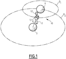
- the geostationary satellite 10 comprises two solar panels 12 and 12 'according to the invention arranged on either side of a body 13 of the satellite 10 in a manner known per se.
- the satellite 10 revolves around the Earth T following an orbit O 1 .
- the Earth then revolves around the Sun S following an O 2 orbit.
- the line E passing through the center of the Sun S and a fixed point of the panel 12 and oriented towards the satellite 10 will be denoted hereafter by the term “direction of illumination E”.
- the voltage of this current ranges for example from 28 V up to 160V, or even up to 350 V or more.
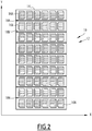
- the solar panels 12, 12 ' are substantially identical to each other. Thus, subsequently, only the solar panel 12 will be explained in detail with particular reference to the figures 2 and 3 .
- the solar panel 12 has for example an elongated shape along a longitudinal axis Y perpendicular to a transverse axis X.
- This shape is for example substantially rectangular.
- the longitudinal axis Y extends along the length of the rectangle and the transverse axis X extends along the width of this rectangle.
- the satellite 10 rotates around the Earth T by following the orbit O 1 for example so that the longitudinal axis Y is perpendicular to the plane comprising this orbit O 1 .
- the longitudinal axis Y is called the North-South axis.
- the solar panel 12 comprises a structure 14, a plurality of photovoltaic cells 16A to 16N capable of generating an electric current and arranged on the structure 14 forming rows along the transverse axis X ,, and a plurality of dielectric barriers 18A to 18N arranged between the rows of cells 16A to 16N and extending along the transverse axis X as will be explained below. Moreover, the first and the last cells of each row are called hereafter end cells.
- the structure 14 is adapted to be fixed to the body 13 of the satellite 10 and has the wiring means necessary to conduct an electric current between the cells 16A to 16N and to the body 13 of the satellite 10.
- Each cell 16A to 16N is capable of producing, for example, an electric current of the order of 0.5A, or of 0.8A, or even of 1.6 A depending on the unit size of the solar cells, which is always larger.
- the cells 16A to 16N are arranged on the structure 14 in nine rows, each row being composed of six cells and extending along the transverse axis X.
- Cells 16A to 16N form a panel surface 19 visible on the figure 3 .
- the panel surface 19 defines a direction P perpendicular to this surface.
- the perpendicular direction P deviates from the lighting direction E at a separation angle ⁇ .
- the separation angle ⁇ varies from 0 ° up to the value of a maximum separation angle ⁇ max .
- the maximum separation angle ⁇ max is equal for example to approximately 23.45 °. The purpose of such a value of the separation angle is to avoid the shadows cast on the panel surface 19.
- Cells 16A to 16N are substantially identical to each other. Furthermore, the barriers 18A to 18N separating the rows of cells are also substantially identical to each other.
- each cell 16A to 16N has a hexagonal shape with two right angles adjacent to the same side, called the long side, and four other angles greater than 90 °, two of these angles being adjacent to a side parallel to the long side, said side short.
- the shape is symmetrical about an axis perpendicular to the short side and the long side.
- each cell 16A to 16N is in the form of a rectangle with two angles shot symmetrically.
- the cells 16A to 16N are arranged in a conventional manner, that is to say so that their long side (or the short side) is perpendicular to the transverse axis X.
- the cells 16A to 16N are connected to each other by the wiring means extending parallel to the transverse axis X and conventionally called interconnectors (not shown on the diagram). figure 2 ).
- the voltage is not very different and is for example between 0.5V and 2.5V depending on the technology of the cells.
- the wiring means connect only two neighboring cells, for example the end cells located on the same side of the panel 12.
- the wiring means connect the cells of the same row transversely and the cells of different rows longitudinally.
- the last cells of the first two rows are connected by the wiring means.
- the voltage between these neighboring cells is for example between 0.5V and 2.5V depending on the technology of the cells.
- each barrier 18A to 18N extends along the transverse axis X substantially between the end cells of the same row, that is to say all along the corresponding row.
- the wiring means between different rows pass by bypassing the corresponding barrier or from below the panel as is conventionally done for each row of cells.
- each barrier 18A to 18N along the corresponding row can be adjusted depending on the arrangement of cells 16A to 16N and the wiring means.
- a barrier 18A to 18N is placed between each pair of cells 16A to 16N between which the voltage is greater than 30 V.
- the barrier will then have to protect the cells exhibiting a high voltage with sufficient distance between cells both in height or grazing.
- the wiring of the neighboring row will then have to bypass or pass through the barrier.
- the barrier may have a notch so that it can be fitted after wiring.
- the barriers 18A to 18N are no longer straight, but form zigzags. In this case, cells 16 to 16N are oriented so that the corresponding barriers 18A to 18N generate as little shadow as possible over its greatest possible length.
- each of the cells 16A, 16B comprises a base element 20A, 20B fixed on the structure 14, a protective element 22A, 22B covering the base element 20A, 20B, and a grid of electrical conductors 24A, 24B arranged between the 'base element 20A, 20B and the protective element 22A, 22B.
- the basic element 20A, 20B is known per se.
- Such an element comprises in particular a conductive plate, a lower layer composed of a P-doped semiconductor and covering the conductive plate, and an upper layer composed of an N -doped semiconductor and covering the lower layer.
- the protective element 22A, 22B is made of a transparent material such as a glass for example, and makes it possible to protect the cell 16A, 16B against the radiative dose while allowing light to pass towards the base element 20A, 20B .
- This element 22A, 22B is also known by the English term “coverglass”.
- the grid 24A, 24B comprises a plurality of conductive wires arranged homogeneously over the entire surface of the base element 20A.
- the grid 24A, 24B is in the form of a comb (visible on the figure 2 ) with the conducting wires extending along the transverse axis X.
- a structure allows light to pass towards the base element 20A, 20B.
- Each of the two cells 16A, 16B defines a lateral contact face 30A, 30B.
- the lateral contact faces 30A, 30B are arranged one opposite the other.
- a conductive wire of each of the grids 24A, 24B runs along the corresponding lateral contact face 30A, 30B.
- the lateral contact faces 30A, 30B are spaced from one another by a distance d.
- the barrier 18A is disposed between the lateral contact faces 30A, 30B in a symmetrical manner.
- the barrier 18A protrudes from the panel surface 19.
- the reference h corresponds to the length of the protruding part extending in the perpendicular direction P, of the barrier 18A relative to the panel surface 19, and the reference ⁇ corresponds to the thickness of the protective elements 22A, 22B.
- the barrier 18A protrudes relative to the ends of the grids 24A, 24B in contact with the protective elements 22A, 22B with a value h + ⁇ .
- This h + ⁇ value is greater than about 10 mm.
- the shortest path between gilles 24A and 24B and in particular between the wires along the lateral contact faces 30A, 30B, by bypassing the barrier 18A is equal to at least approximately 20 mm.
- the barrier 18A is a thin plate fixed to the structure 14 and made, for example, of glass or of a polyimide polymer, in particular in the form of the material known under the name of Kapton® or UPILEX®.
- the barrier 18A can be made of any dielectric material.
- dielectrics with good temperature resistance Polyimide Kapton TM, Teflon TM, Covergalss all types, etc.
- the material of the barrier 18A is flexible.
- the barrier 18A is adapted to be folded in the space delimited between the two lateral contact faces 30A and 30B without protruding from the panel surface 19.
- Such a configuration of the barrier 18A makes it possible for example to keep it folded during the launch of the satellite and its positioning, that is to say, before deployment of the solar panels 12, 12 '.
- the cells 16A and 16B are arranged so that the shadow generated by the barrier 18A when the direction perpendicular P to the panel surface 19 deviates from the lighting direction E of the maximum separation angle ⁇ max , is located substantially outside each of the two cells 30A, 30B.
- the distance d between the lateral contact faces 30A, 30B of the cells 16A, 16B is for example between 6 mm and 12 mm, preferably between 8 mm and 10 mm, and advantageously equal to approximately 9 mm.
- the barrier 18A is therefore spaced from each of the lateral contact faces 30A, 30B by approximately 4.5 mm.
- a dielectric barrier inserted between two lateral cell contact faces and protruding from the panel surface makes it possible to lengthen this path and thus reduce the risk of an electric arc forming.
- the minimum value of the shortest path between conductive components of adjacent photovoltaic cells should be around 20 mm. This is the case when the h + ⁇ value is about 10 mm.
- the adjacent cells are separated from one another only so that the barrier does not generate a shadow cast on the useful surface of the cells even when the lighting direction E and the perpendicular direction P form the maximum separation angle ⁇ max . This then makes it possible to keep the same productivity of the panel according to the invention with respect to a conventional panel and this whatever the position of the satellite.
- the flexibility of the barriers ensures that the presence of the barriers on the panels does not require structural change of these panels.
- the solar panels according to the invention can be folded on top of each other during the launch phase of the satellite, in particular, without the barriers being an obstacle to this folding.
- a solar panel 112 according to a second embodiment of the invention is illustrated in figure 4 .
- the solar panel 112 is similar to the solar panel 12 described above and comprises in particular a structure 14 and photovoltaic cells 16A to 16N substantially identical to those described above.
- the solar panel 112 further includes a plurality of barriers 118A to 118N which differ from the previously described barriers 18A to 18N only in their shape in cross section.
- each barrier 118A to 118N has an isosceles triangle shape in its cross section.
- the length of the base of this triangle is equal to the value of the distance d mentioned above, the triangle protruding from the panel surface 19 by the same value h mentioned above.
- the angle ⁇ of the triangle facing the base is equal to approximately two angles of maximum separation ⁇ max .
- the barriers 118A to 118N make it possible to minimize the risk of establishing an electric arc between each pair of adjacent cells and do not generate a shadow cast on these cells.
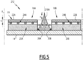
- a solar panel 212 according to a third embodiment of the invention is illustrated in figure 5 .
- the solar panel 212 is similar to the solar panel 112 described above and comprises in particular a structure 14 and photovoltaic cells 16A to 16N substantially identical to those described above.
- Solar panel 212 further includes a plurality of barriers 218A to 218N which differ from barriers 118A to 118N described above in that each barrier 218A to 218N is in the form of a concentrator.
- each barrier 218A to 218N has a curvilinear isosceles triangle shape in its cross section with a rectilinear base.
- the length of the base of this triangle is equal to the value of the distance d mentioned above, the triangle protruding from the panel surface 19 by the same value h mentioned above.
- the angle ⁇ of the triangle facing the base is equal to approximately two angles of maximum separation ⁇ max .
- the surface of the barriers 218A to 218N exposed to the rays of the Sun S is covered with a reflective material.
- the shape of the curvilinear faces of the barriers 218A to 218N is adapted to reflect the rays towards the corresponding cells.
- the barriers 218A to 218N make it possible to minimize the risk of an electric arc establishing between each pair of adjacent cells and do not generate a shadow cast on these cells.
- the productivity of the solar panel 213 is improved by virtue of the barriers 218A to 218N in the form of the concentrators.
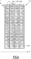
- a solar panel 312 according to a fourth embodiment of the invention is illustrated in figure 6 .
- the solar panel 312 is similar to the solar panel 12 described above and notably comprises a structure 14.
- the solar panel 312 further comprises a plurality of photovoltaic cells 316A to 316N arranged on the structure 14 forming rows along the longitudinal axis Y and a plurality of barriers 318A to 318N arranged between the rows of cells 316A to 316N.
- the first and the last cells of each row are called hereafter end cells.
- the solar panel 312 differs from the panels described above only by the arrangement of the cells 316A to 316N on the structure 14.
- the cells 316A to 316N are arranged on the structure 14 in four rows, each row being composed of twelve cells at most and extending along the longitudinal axis Y. figure 6 , only the first cells 316A and 316B of the first two rows and the last cell 316N of the last row bear references.
- the cells 316A to 316N are connected to each other by the wiring means extending parallel to the longitudinal axis Y.
- the voltage is not very different and is for example between 0.5V and 2.5V depending on the technology of the cells.
- the wiring means connect the corresponding cells, and preferably end cells, bypassing the corresponding barrier 318A to 318N.
- the barriers 318A to 318N extend throughout the corresponding rows.
- the extent of the barriers 318A to 318N can be shortened in the places where the wiring means connect two cells of different rows taking into account a relatively low voltage between these cells.
- a barrier 318A to 318N is placed between each pair of cells 316A to 316N between which the voltage is greater than 30 V.
- Each barrier 318A to 318B is analogous to one of the barriers 18A, 118A or 218A described above.
- each barrier 318A to 318N protrudes from the panel surface 19 by the same value h mentioned above, to minimize the risk of establishing an electric arc.
- the arrangement of the barriers 318A to 318N along the longitudinal axis Y constitutes a particular advantage of the invention according to the fourth embodiment. Indeed, such an arrangement of the barriers 318A to 318N relative to the Sun S means that the barriers 318A to 318N do not generate a shadow cast on the cells.
- the distance d between the lateral contact faces of each pair of cells 316A to 316N belonging to the different rows can be advantageously reduced in order to make the arrangement of these cells on the structure 14 more compact.
- this distance d is for example equal to 0.9 +/- 0.3 mm.
- the cells on the figure 6 are arranged on the structure 14 in a particularly compact manner, in particular along the longitudinal axis Y and this without modifying the usual dimensions of a solar panel without barrier.
- the barrier can be continuous or discontinuous when the voltage drops below 30 V or to facilitate a folding mode or when the gap between cells is not straight due to the shape of the cells (trapezoidal for example).
- the dielectric barrier can be formed from a shape memory material, to regain the desired shape after deployment or illumination (by energy transmission).
- the solar panel according to the invention can be on board any mobile device other than a satellite or in general, can be used independently of any mobile device, for example in a fixed configuration on the surface. earthly.
- the distance d between the lateral contact faces of each pair of neighboring cells is less than each dimension of these cells (width, length and height), advantageously is at least two times less than each of these dimensions. Furthermore, preferably, this distance d is less than 30 mm, advantageously less than 20 mm and even more advantageously less than 10 mm.
Landscapes
- Engineering & Computer Science (AREA)
- Life Sciences & Earth Sciences (AREA)
- Sustainable Development (AREA)
- Remote Sensing (AREA)
- Aviation & Aerospace Engineering (AREA)
- Photovoltaic Devices (AREA)
- Sustainable Energy (AREA)
Claims (12)
- Solarpanel (12; 112; 212; 312), umfassend:- eine Struktur (14) in Kontakt mit einem umgebenden Medium;- mindestens zwei Photovoltaikzellen (16A, 16B; 316A, 316B), wobei jede Zelle (16A, 16B; 316A, 316B) eine seitliche Kontaktfläche (30A, 30B) definiert und ein Basiselement (20A, 20B), ein Gitter von elektrischen Leitern (24A, 24B) und ein Schutzelement (22A, 22B) aus transparentem Material umfasst, wobei das Gitter (24A, 24B) zwischen dem Schutzelement (22A, 22B) und dem Basiselement (20A, 20B) angeordnet ist und mindestens einen Leitungsdraht umfasst, der an der seitlichen Kontaktfläche (30A, 30B) der Zelle (16A, 16B; 316A, 316B) entlangläuft;wobei die zwei Zellen (16A, 16B; 316A, 316B) auf der Struktur (14) so angeordnet sind, dass mindestens ein Teil jeder der seitlichen Kontaktflächen (30A, 30B) gegenüber dem anderen Teil angeordnet ist und so, dass die Schutzelemente (22A, 22B) dieser Zellen (16A, 16B; 316A, 316B) eine Paneloberfläche (19) bilden;
wobei die Zellen (16A, 16B; 316A, 316B) so angeordnet sind, dass der kürzeste Weg, der durch das umgebende Medium zwischen den gegenüberliegenden Teilen der seitlichen Kontaktflächen (30A, 30B) der zwei Zellen (16A, 16B; 316A, 316B) verläuft, mindestens ungefähr 20 mm beträgt,
wobei das Solarpanel (12; 112; 212; 312) dadurch gekennzeichnet ist, dass es weiter eine Schranke (18A; 118A; 218A; 318A) aus dielektrischem Material umfasst, die auf der Struktur (14) zwischen den seitlichen Kontaktflächen (30A, 30B) der zwei Photovoltaikzellen (16A, 16B; 316A, 316B) angeordnet ist, sie sich gemäß den gegenüberliegenden Teilen dieser Flächen (30A, 30B) erstreckt und in Bezug auf die Paneloberfläche (19) vorragt, wobei der kürzeste Weg zwischen den gegenüberliegenden Teilen der seitlichen Kontaktflächen (30A, 30B) durch Umgehung der Schranke (18A; 118A; 218A; 318A) berechnet wird, wobei die Schranke (18A; 118A; 218A; 318A) zwischen jedem Paar von Photovoltaikzellen (16A, 16B; 316A, 316B) angeordnet ist, zwischen denen die Spannung höher ist als 30 V. - Panel (12; 112; 212; 312) nach Anspruch 1, dadurch gekennzeichnet:- dass es ausgelegt ist, um in einem Medium zu funktionieren, in dem die zu der Paneloberfläche (19) senkrechte Richtung (P) von einer Beleuchtungsrichtung (E) um einen maximalen Abweichungswinkel (amax) von weniger als 90° abweicht, wobei die Beleuchtungsrichtung (E) durch eine Gerade definiert wird, die durch die Mitte einer Beleuchtungsquelle (S) und eines vorbestimmten Punkts des Panels verläuft; und- dass die Schranke (18A; 118A; 218A; 318A) und/oder die Zellen (16A, 16B) so angeordnet sind, dass der Schatten, der von der Schranke (18A; 118A; 218A; 318A) erzeugt wird, wenn die zu der Paneloberfläche (19) senkrechte Richtung (P) von der Beleuchtungsrichtung (E) um den maximalen Abweichungswinkel (amax) abweicht, im Wesentlichen außerhalb von jeder der zwei Zellen (16A, 16B; 316A, 316B) liegt.
- Panel (12; 112; 212; 312) nach Anspruch 1 oder 2, dadurch gekennzeichnet, dass es sich an Bord in einem Raumfahrzeug (10) befindet.
- Panel (12; 112; 212; 312) nach einem der Ansprüche 1 bis 3, dadurch gekennzeichnet, dass die Schranke (18A; 118A; 218A; 318A) in Bezug auf die Paneloberfläche (19) um mindestens 10 mm vorragt.
- Panel (12; 112; 212) nach einem der Ansprüche 1 bis 4, dadurch gekennzeichnet, dass die gegenüberliegenden Teile der zwei Zellen um mindestens ungefähr 9 mm beabstandet sind.
- Panel (112; 212; 312) nach einem der Ansprüche 2 bis 5, dadurch gekennzeichnet, dass der Querschnitt der Schranke (118A; 218A; 318A) ein gleichschenkliges Dreieck bildet, dessen Basis an die Struktur (14) angrenzt, wobei der Winkel gegenüber der Basis zwei Mal größer ist als der maximale Abweichungswinkel (amax).
- Panel (312) nach einem der vorstehenden Ansprüche, dadurch gekennzeichnet:- dass die Struktur (14) eine längliche Form gemäß einer Längsachse (Y) senkrecht zu einer Querachse (X) aufweist; und- dass das Gitter jeder Zelle (316A, 316B) eine Vielzahl von Leitungsdrähten umfasst, die sich gemäß der Längsachse (Y) erstrecken.
- Panel (312) nach Anspruch 7, dadurch gekennzeichnet, dass sich das Gitter jeder Zelle (316A, 316B) in Form eines Kamms darstellt, dessen Zähne von den Leitungsdrähten gebildet werden, die sich gemäß der Längsachse (Y) erstrecken.
- Panel (312) nach Anspruch 7 oder 8, dadurch gekennzeichnet:- dass es sich an Bord in einem Raumfahrzeug (10) befindet, das gemäß einer Umlaufbahn (O1) dreht; und- dass die Längsachse (Y) senkrecht auf die Ebene verläuft, welche die Umlaufbahn (O1) umfasst.
- Panel (12; 112; 212; 312) nach einem der Ansprüche 1 bis 9, dadurch gekennzeichnet, dass die Schranke (18A; 118A; 218A; 318A) aus einem flexiblen Material hergestellt ist, wobei die Schranke (18A; 118A; 218A; 318A) angepasst ist, um in dem Raum, der von den zwei seitlichen Kontaktflächen (30A, 30B) gebildet wird, gefaltet zu werden, ohne in Bezug auf die Paneloberfläche (19) vorzuspringen.
- Panel (12; 112; 212; 312) nach einem der Ansprüche 1 bis 10, dadurch gekennzeichnet, dass die Schranke (18A; 118A; 218A; 318A) aus einem Polyimid-Polymer hergestellt ist.
- Panel (212) nach einem der Ansprüche 1 bis 11, dadurch gekennzeichnet, dass die Schranke (218A) ein Konzentrator ist.
Applications Claiming Priority (1)
| Application Number | Priority Date | Filing Date | Title |
|---|---|---|---|
| FR1755121A FR3067519B1 (fr) | 2017-06-08 | 2017-06-08 | Panneau solaire comportant notamment une structure et au moins deux cellules photovoltaiques |
Publications (2)
| Publication Number | Publication Date |
|---|---|
| EP3413355A1 EP3413355A1 (de) | 2018-12-12 |
| EP3413355B1 true EP3413355B1 (de) | 2021-03-03 |
Family
ID=60627687
Family Applications (1)
| Application Number | Title | Priority Date | Filing Date |
|---|---|---|---|
| EP18176113.1A Active EP3413355B1 (de) | 2017-06-08 | 2018-06-05 | Solarpanel, das insbesondere eine fotovoltaikstruktur und mindestens zwei fotovoltaikzellen umfasst |
Country Status (4)
| Country | Link |
|---|---|
| US (1) | US11081607B2 (de) |
| EP (1) | EP3413355B1 (de) |
| JP (1) | JP2018207111A (de) |
| FR (1) | FR3067519B1 (de) |
Families Citing this family (1)
| Publication number | Priority date | Publication date | Assignee | Title |
|---|---|---|---|---|
| US11575058B2 (en) * | 2017-06-30 | 2023-02-07 | Mitsubishi Electric Corporation | Solar power generator, solar array wing, and space structure |
Family Cites Families (13)
| Publication number | Priority date | Publication date | Assignee | Title |
|---|---|---|---|---|
| US4574160A (en) * | 1984-09-28 | 1986-03-04 | The Standard Oil Company | Flexible, rollable photovoltaic cell module |
| WO2000079593A1 (en) * | 1999-06-21 | 2000-12-28 | Aec-Able Engineering Co., Inc. | Solar cell array |
| US6091017A (en) * | 1999-08-23 | 2000-07-18 | Composite Optics Incorporated | Solar concentrator array |
| US6188012B1 (en) * | 1999-11-10 | 2001-02-13 | Tecstar Power Systems | Methods and systems for a solar cell concentrator |
| EP1174342A1 (de) * | 2000-07-20 | 2002-01-23 | Université de Liège | Solarkonzentrator |
| FR2834584B1 (fr) * | 2002-01-07 | 2005-07-15 | Cit Alcatel | Dispositif concentrateur d'energie solaire pour vehicule spatial et panneau generateur solaire |
| DE10239845C1 (de) * | 2002-08-29 | 2003-12-24 | Day4 Energy Inc | Elektrode für fotovoltaische Zellen, fotovoltaische Zelle und fotovoltaischer Modul |
| US7732229B2 (en) * | 2004-09-18 | 2010-06-08 | Nanosolar, Inc. | Formation of solar cells with conductive barrier layers and foil substrates |
| US8212139B2 (en) * | 2008-01-18 | 2012-07-03 | Tenksolar, Inc. | Thin-film photovoltaic module |
| JP2010021350A (ja) * | 2008-07-10 | 2010-01-28 | Mitsubishi Electric Corp | 太陽電池および太陽電池パネル |
| JP5459766B2 (ja) * | 2009-10-01 | 2014-04-02 | Nec東芝スペースシステム株式会社 | 太陽電池パネル、太陽電池パネルの帯電抑制方法及び人工衛星搭載用太陽光発電装置 |
| JP5231499B2 (ja) * | 2010-09-06 | 2013-07-10 | シャープ株式会社 | 太陽電池モジュール |
| US10529868B2 (en) * | 2014-10-31 | 2020-01-07 | Byd Company Limited | Solar cell array, solar cell module and manufacturing method thereof |
-
2017
- 2017-06-08 FR FR1755121A patent/FR3067519B1/fr active Active
-
2018
- 2018-06-04 US US15/996,847 patent/US11081607B2/en active Active
- 2018-06-05 EP EP18176113.1A patent/EP3413355B1/de active Active
- 2018-06-08 JP JP2018110065A patent/JP2018207111A/ja active Pending
Non-Patent Citations (3)
| Title |
|---|
| ANONYMOUS: "Cubesat solar panels complete set - CubeSatShop.com", 20 August 2016 (2016-08-20), XP055665726, Retrieved from the Internet <URL:https://web.archive.org/web/20160820055526/http://www.cubesatshop.com/product/cubesat-solar-panels-complete-set/> [retrieved on 20200206] * |
| ANONYMOUS: "ISIS", 1 January 2016 (2016-01-01), pages 1 - 2, XP055665593, Retrieved from the Internet <URL:https://www.isispace.nl/wp-content/uploads/2016/02/ISIS-Solar-Panels-Brochure-v2R-web.pdf> [retrieved on 20200205] * |
| JUSSI HEMMO: "Electrical Power Systems for Finnish Nanosatellites", 15 November 2013 (2013-11-15), XP055665596, Retrieved from the Internet <URL:https://pdfs.semanticscholar.org/fcdd/40c00818eff8ffe6effbc17134308826ef2f.pdf> [retrieved on 20200205] * |
Also Published As
| Publication number | Publication date |
|---|---|
| US11081607B2 (en) | 2021-08-03 |
| EP3413355A1 (de) | 2018-12-12 |
| US20180358496A1 (en) | 2018-12-13 |
| FR3067519A1 (fr) | 2018-12-14 |
| FR3067519B1 (fr) | 2019-07-26 |
| JP2018207111A (ja) | 2018-12-27 |
Similar Documents
| Publication | Publication Date | Title |
|---|---|---|
| EP3147952B1 (de) | Flexibler solargenerator, der mit einem elektrischen schutz gegen einschläge von himmelskörpern ausgestattet ist, raumschiff und satellit, die mindestens einen solchen solargenerator umfassen | |
| CA2380665C (fr) | Radiateur deployable pour engin spatial | |
| EP2643215B1 (de) | Vorrichtung zur überwachung der lage eines satelliten und verfahren zur steuerung eines mit dieser vorrichtung ausgestatteten satelliten | |
| EP1548847A2 (de) | Solargenerator-Paneel und entsprechender Satellit | |
| EP0436425B1 (de) | System zur Steuerung der Lage eines stabilisierten Satelliten durch Solarzellen | |
| FR2834584A1 (fr) | Dispositif concentrateur d'energie solaire pour vehicule spatial et panneau generateur solaire | |
| FR2969580A1 (fr) | Structure deployable formant une antenne equipee d'un generateur solaire pour un satellite | |
| WO2002074623A1 (fr) | Panneau solaire ayant des bornes electriques reparties sur sa surface | |
| EP3079988A1 (de) | Entfaltbarer radiator für einen auf drei achsen stabilisierten satelliten | |
| EP3413355B1 (de) | Solarpanel, das insbesondere eine fotovoltaikstruktur und mindestens zwei fotovoltaikzellen umfasst | |
| EP3413356B1 (de) | Solarpanel, das eine struktur, mindestens zwei fotovoltaikzellen und eine barriere umfasst | |
| EP4199118A1 (de) | Verfahren zur thermischen aktivierung einer passivierungsschicht | |
| FR2473011A1 (fr) | Agencement de satellite artificiel pourvu de generateurs solaires et d'antennes deployables | |
| CA3162035C (fr) | Module photovoltaique et generateur solaire flexible de satellite | |
| FR3086371A1 (fr) | Panneau radiant destine a etre installe a l'interieur d'un habitacle de vehicule | |
| EP1705718A1 (de) | Photovoltaischer Solargenerator mit Entladungsstromblockierung | |
| EP1974394B1 (de) | Solargenerator mit konzentrator primärer lichtbögen | |
| EP4631109A1 (de) | Doppelseitiges fotovoltaisches modul | |
| WO2013167564A2 (fr) | Module photovoltaïque et procede de realisation d'un tel module | |
| FR3131443A1 (fr) | Panneau solaire comportant notamment une pluralité de zones de composants électroniques connectées entre elles par une pluralité de câbles électriques. | |
| FR2864346A1 (fr) | Panneau generateur solaire et satellite associe | |
| EP4199122A1 (de) | Photovoltaische zelle mit passiven kontakten und antireflexionsbeschichtung | |
| FR2711111A1 (fr) | Engin spatial à voile solaire et procédé de pilotage d'un tel engin. | |
| FR2568853A1 (fr) | Procede pour augmenter en orbite de transfert la puissance electrique du generateur solaire d'un satellite artificiel stabilise par mise en rotation, et agencement de satellite pour mise en oeuvre de ce procede | |
| FR2983643A1 (fr) | Dispositif et procede d'interconnexion electrique de cellules photovoltaiques |
Legal Events
| Date | Code | Title | Description |
|---|---|---|---|
| PUAI | Public reference made under article 153(3) epc to a published international application that has entered the european phase |
Free format text: ORIGINAL CODE: 0009012 |
|
| STAA | Information on the status of an ep patent application or granted ep patent |
Free format text: STATUS: THE APPLICATION HAS BEEN PUBLISHED |
|
| AK | Designated contracting states |
Kind code of ref document: A1 Designated state(s): AL AT BE BG CH CY CZ DE DK EE ES FI FR GB GR HR HU IE IS IT LI LT LU LV MC MK MT NL NO PL PT RO RS SE SI SK SM TR |
|
| AX | Request for extension of the european patent |
Extension state: BA ME |
|
| STAA | Information on the status of an ep patent application or granted ep patent |
Free format text: STATUS: REQUEST FOR EXAMINATION WAS MADE |
|
| 17P | Request for examination filed |
Effective date: 20190611 |
|
| RBV | Designated contracting states (corrected) |
Designated state(s): AL AT BE BG CH CY CZ DE DK EE ES FI FR GB GR HR HU IE IS IT LI LT LU LV MC MK MT NL NO PL PT RO RS SE SI SK SM TR |
|
| STAA | Information on the status of an ep patent application or granted ep patent |
Free format text: STATUS: EXAMINATION IS IN PROGRESS |
|
| 17Q | First examination report despatched |
Effective date: 20200213 |
|
| GRAP | Despatch of communication of intention to grant a patent |
Free format text: ORIGINAL CODE: EPIDOSNIGR1 |
|
| STAA | Information on the status of an ep patent application or granted ep patent |
Free format text: STATUS: GRANT OF PATENT IS INTENDED |
|
| INTG | Intention to grant announced |
Effective date: 20201119 |
|
| GRAS | Grant fee paid |
Free format text: ORIGINAL CODE: EPIDOSNIGR3 |
|
| GRAA | (expected) grant |
Free format text: ORIGINAL CODE: 0009210 |
|
| STAA | Information on the status of an ep patent application or granted ep patent |
Free format text: STATUS: THE PATENT HAS BEEN GRANTED |
|
| AK | Designated contracting states |
Kind code of ref document: B1 Designated state(s): AL AT BE BG CH CY CZ DE DK EE ES FI FR GB GR HR HU IE IS IT LI LT LU LV MC MK MT NL NO PL PT RO RS SE SI SK SM TR |
|
| REG | Reference to a national code |
Ref country code: GB Ref legal event code: FG4D Free format text: NOT ENGLISH |
|
| REG | Reference to a national code |
Ref country code: AT Ref legal event code: REF Ref document number: 1368170 Country of ref document: AT Kind code of ref document: T Effective date: 20210315 Ref country code: CH Ref legal event code: EP |
|
| REG | Reference to a national code |
Ref country code: DE Ref legal event code: R096 Ref document number: 602018013255 Country of ref document: DE |
|
| REG | Reference to a national code |
Ref country code: IE Ref legal event code: FG4D Free format text: LANGUAGE OF EP DOCUMENT: FRENCH |
|
| REG | Reference to a national code |
Ref country code: LT Ref legal event code: MG9D |
|
| PG25 | Lapsed in a contracting state [announced via postgrant information from national office to epo] |
Ref country code: NO Free format text: LAPSE BECAUSE OF FAILURE TO SUBMIT A TRANSLATION OF THE DESCRIPTION OR TO PAY THE FEE WITHIN THE PRESCRIBED TIME-LIMIT Effective date: 20210603 Ref country code: LT Free format text: LAPSE BECAUSE OF FAILURE TO SUBMIT A TRANSLATION OF THE DESCRIPTION OR TO PAY THE FEE WITHIN THE PRESCRIBED TIME-LIMIT Effective date: 20210303 Ref country code: BG Free format text: LAPSE BECAUSE OF FAILURE TO SUBMIT A TRANSLATION OF THE DESCRIPTION OR TO PAY THE FEE WITHIN THE PRESCRIBED TIME-LIMIT Effective date: 20210603 Ref country code: GR Free format text: LAPSE BECAUSE OF FAILURE TO SUBMIT A TRANSLATION OF THE DESCRIPTION OR TO PAY THE FEE WITHIN THE PRESCRIBED TIME-LIMIT Effective date: 20210604 Ref country code: FI Free format text: LAPSE BECAUSE OF FAILURE TO SUBMIT A TRANSLATION OF THE DESCRIPTION OR TO PAY THE FEE WITHIN THE PRESCRIBED TIME-LIMIT Effective date: 20210303 Ref country code: HR Free format text: LAPSE BECAUSE OF FAILURE TO SUBMIT A TRANSLATION OF THE DESCRIPTION OR TO PAY THE FEE WITHIN THE PRESCRIBED TIME-LIMIT Effective date: 20210303 |
|
| REG | Reference to a national code |
Ref country code: NL Ref legal event code: MP Effective date: 20210303 |
|
| REG | Reference to a national code |
Ref country code: AT Ref legal event code: MK05 Ref document number: 1368170 Country of ref document: AT Kind code of ref document: T Effective date: 20210303 |
|
| PG25 | Lapsed in a contracting state [announced via postgrant information from national office to epo] |
Ref country code: PL Free format text: LAPSE BECAUSE OF FAILURE TO SUBMIT A TRANSLATION OF THE DESCRIPTION OR TO PAY THE FEE WITHIN THE PRESCRIBED TIME-LIMIT Effective date: 20210303 Ref country code: LV Free format text: LAPSE BECAUSE OF FAILURE TO SUBMIT A TRANSLATION OF THE DESCRIPTION OR TO PAY THE FEE WITHIN THE PRESCRIBED TIME-LIMIT Effective date: 20210303 Ref country code: RS Free format text: LAPSE BECAUSE OF FAILURE TO SUBMIT A TRANSLATION OF THE DESCRIPTION OR TO PAY THE FEE WITHIN THE PRESCRIBED TIME-LIMIT Effective date: 20210303 Ref country code: SE Free format text: LAPSE BECAUSE OF FAILURE TO SUBMIT A TRANSLATION OF THE DESCRIPTION OR TO PAY THE FEE WITHIN THE PRESCRIBED TIME-LIMIT Effective date: 20210303 |
|
| PG25 | Lapsed in a contracting state [announced via postgrant information from national office to epo] |
Ref country code: NL Free format text: LAPSE BECAUSE OF FAILURE TO SUBMIT A TRANSLATION OF THE DESCRIPTION OR TO PAY THE FEE WITHIN THE PRESCRIBED TIME-LIMIT Effective date: 20210303 |
|
| PG25 | Lapsed in a contracting state [announced via postgrant information from national office to epo] |
Ref country code: AT Free format text: LAPSE BECAUSE OF FAILURE TO SUBMIT A TRANSLATION OF THE DESCRIPTION OR TO PAY THE FEE WITHIN THE PRESCRIBED TIME-LIMIT Effective date: 20210303 Ref country code: SM Free format text: LAPSE BECAUSE OF FAILURE TO SUBMIT A TRANSLATION OF THE DESCRIPTION OR TO PAY THE FEE WITHIN THE PRESCRIBED TIME-LIMIT Effective date: 20210303 Ref country code: CZ Free format text: LAPSE BECAUSE OF FAILURE TO SUBMIT A TRANSLATION OF THE DESCRIPTION OR TO PAY THE FEE WITHIN THE PRESCRIBED TIME-LIMIT Effective date: 20210303 Ref country code: EE Free format text: LAPSE BECAUSE OF FAILURE TO SUBMIT A TRANSLATION OF THE DESCRIPTION OR TO PAY THE FEE WITHIN THE PRESCRIBED TIME-LIMIT Effective date: 20210303 |
|
| PG25 | Lapsed in a contracting state [announced via postgrant information from national office to epo] |
Ref country code: PT Free format text: LAPSE BECAUSE OF FAILURE TO SUBMIT A TRANSLATION OF THE DESCRIPTION OR TO PAY THE FEE WITHIN THE PRESCRIBED TIME-LIMIT Effective date: 20210705 Ref country code: RO Free format text: LAPSE BECAUSE OF FAILURE TO SUBMIT A TRANSLATION OF THE DESCRIPTION OR TO PAY THE FEE WITHIN THE PRESCRIBED TIME-LIMIT Effective date: 20210303 Ref country code: SK Free format text: LAPSE BECAUSE OF FAILURE TO SUBMIT A TRANSLATION OF THE DESCRIPTION OR TO PAY THE FEE WITHIN THE PRESCRIBED TIME-LIMIT Effective date: 20210303 Ref country code: IS Free format text: LAPSE BECAUSE OF FAILURE TO SUBMIT A TRANSLATION OF THE DESCRIPTION OR TO PAY THE FEE WITHIN THE PRESCRIBED TIME-LIMIT Effective date: 20210703 |
|
| REG | Reference to a national code |
Ref country code: DE Ref legal event code: R097 Ref document number: 602018013255 Country of ref document: DE |
|
| PLBE | No opposition filed within time limit |
Free format text: ORIGINAL CODE: 0009261 |
|
| STAA | Information on the status of an ep patent application or granted ep patent |
Free format text: STATUS: NO OPPOSITION FILED WITHIN TIME LIMIT |
|
| PG25 | Lapsed in a contracting state [announced via postgrant information from national office to epo] |
Ref country code: ES Free format text: LAPSE BECAUSE OF FAILURE TO SUBMIT A TRANSLATION OF THE DESCRIPTION OR TO PAY THE FEE WITHIN THE PRESCRIBED TIME-LIMIT Effective date: 20210303 Ref country code: MC Free format text: LAPSE BECAUSE OF FAILURE TO SUBMIT A TRANSLATION OF THE DESCRIPTION OR TO PAY THE FEE WITHIN THE PRESCRIBED TIME-LIMIT Effective date: 20210303 Ref country code: AL Free format text: LAPSE BECAUSE OF FAILURE TO SUBMIT A TRANSLATION OF THE DESCRIPTION OR TO PAY THE FEE WITHIN THE PRESCRIBED TIME-LIMIT Effective date: 20210303 Ref country code: DK Free format text: LAPSE BECAUSE OF FAILURE TO SUBMIT A TRANSLATION OF THE DESCRIPTION OR TO PAY THE FEE WITHIN THE PRESCRIBED TIME-LIMIT Effective date: 20210303 |
|
| REG | Reference to a national code |
Ref country code: CH Ref legal event code: PL |
|
| 26N | No opposition filed |
Effective date: 20211206 |
|
| PG25 | Lapsed in a contracting state [announced via postgrant information from national office to epo] |
Ref country code: SI Free format text: LAPSE BECAUSE OF FAILURE TO SUBMIT A TRANSLATION OF THE DESCRIPTION OR TO PAY THE FEE WITHIN THE PRESCRIBED TIME-LIMIT Effective date: 20210303 |
|
| PG25 | Lapsed in a contracting state [announced via postgrant information from national office to epo] |
Ref country code: LU Free format text: LAPSE BECAUSE OF NON-PAYMENT OF DUE FEES Effective date: 20210605 |
|
| PG25 | Lapsed in a contracting state [announced via postgrant information from national office to epo] |
Ref country code: LI Free format text: LAPSE BECAUSE OF NON-PAYMENT OF DUE FEES Effective date: 20210630 Ref country code: IE Free format text: LAPSE BECAUSE OF NON-PAYMENT OF DUE FEES Effective date: 20210605 Ref country code: CH Free format text: LAPSE BECAUSE OF NON-PAYMENT OF DUE FEES Effective date: 20210630 |
|
| PG25 | Lapsed in a contracting state [announced via postgrant information from national office to epo] |
Ref country code: IS Free format text: LAPSE BECAUSE OF FAILURE TO SUBMIT A TRANSLATION OF THE DESCRIPTION OR TO PAY THE FEE WITHIN THE PRESCRIBED TIME-LIMIT Effective date: 20210703 |
|
| GBPC | Gb: european patent ceased through non-payment of renewal fee |
Effective date: 20220605 |
|
| PG25 | Lapsed in a contracting state [announced via postgrant information from national office to epo] |
Ref country code: GB Free format text: LAPSE BECAUSE OF NON-PAYMENT OF DUE FEES Effective date: 20220605 |
|
| PG25 | Lapsed in a contracting state [announced via postgrant information from national office to epo] |
Ref country code: CY Free format text: LAPSE BECAUSE OF FAILURE TO SUBMIT A TRANSLATION OF THE DESCRIPTION OR TO PAY THE FEE WITHIN THE PRESCRIBED TIME-LIMIT Effective date: 20210303 |
|
| PG25 | Lapsed in a contracting state [announced via postgrant information from national office to epo] |
Ref country code: HU Free format text: LAPSE BECAUSE OF FAILURE TO SUBMIT A TRANSLATION OF THE DESCRIPTION OR TO PAY THE FEE WITHIN THE PRESCRIBED TIME-LIMIT; INVALID AB INITIO Effective date: 20180605 |
|
| PG25 | Lapsed in a contracting state [announced via postgrant information from national office to epo] |
Ref country code: MK Free format text: LAPSE BECAUSE OF FAILURE TO SUBMIT A TRANSLATION OF THE DESCRIPTION OR TO PAY THE FEE WITHIN THE PRESCRIBED TIME-LIMIT Effective date: 20210303 |
|
| PG25 | Lapsed in a contracting state [announced via postgrant information from national office to epo] |
Ref country code: MT Free format text: LAPSE BECAUSE OF FAILURE TO SUBMIT A TRANSLATION OF THE DESCRIPTION OR TO PAY THE FEE WITHIN THE PRESCRIBED TIME-LIMIT Effective date: 20210303 |
|
| REG | Reference to a national code |
Ref country code: DE Ref legal event code: R079 Ref document number: 602018013255 Country of ref document: DE Free format text: PREVIOUS MAIN CLASS: H01L0031042000 Ipc: H10F0019000000 |
|
| PGFP | Annual fee paid to national office [announced via postgrant information from national office to epo] |
Ref country code: DE Payment date: 20250529 Year of fee payment: 8 |
|
| PGFP | Annual fee paid to national office [announced via postgrant information from national office to epo] |
Ref country code: BE Payment date: 20250619 Year of fee payment: 8 |
|
| PGFP | Annual fee paid to national office [announced via postgrant information from national office to epo] |
Ref country code: FR Payment date: 20250521 Year of fee payment: 8 |
|
| PGFP | Annual fee paid to national office [announced via postgrant information from national office to epo] |
Ref country code: IT Payment date: 20250617 Year of fee payment: 8 |
|
| PG25 | Lapsed in a contracting state [announced via postgrant information from national office to epo] |
Ref country code: TR Free format text: LAPSE BECAUSE OF FAILURE TO SUBMIT A TRANSLATION OF THE DESCRIPTION OR TO PAY THE FEE WITHIN THE PRESCRIBED TIME-LIMIT Effective date: 20210303 |