EP3414613B1 - Verfahren und vorrichtung zum betrieb einer elektrooptischen anzeige im weissmodus - Google Patents
Verfahren und vorrichtung zum betrieb einer elektrooptischen anzeige im weissmodus Download PDFInfo
- Publication number
- EP3414613B1 EP3414613B1 EP17750663.1A EP17750663A EP3414613B1 EP 3414613 B1 EP3414613 B1 EP 3414613B1 EP 17750663 A EP17750663 A EP 17750663A EP 3414613 B1 EP3414613 B1 EP 3414613B1
- Authority
- EP
- European Patent Office
- Prior art keywords
- state
- pixel
- display
- image
- black
- Prior art date
- Legal status (The legal status is an assumption and is not a legal conclusion. Google has not performed a legal analysis and makes no representation as to the accuracy of the status listed.)
- Active
Links
Images



Classifications
-
- G—PHYSICS
- G02—OPTICS
- G02B—OPTICAL ELEMENTS, SYSTEMS OR APPARATUS
- G02B26/00—Optical devices or arrangements for the control of light using movable or deformable optical elements
- G02B26/02—Optical devices or arrangements for the control of light using movable or deformable optical elements for controlling the intensity of light
-
- G—PHYSICS
- G02—OPTICS
- G02F—OPTICAL DEVICES OR ARRANGEMENTS FOR THE CONTROL OF LIGHT BY MODIFICATION OF THE OPTICAL PROPERTIES OF THE MEDIA OF THE ELEMENTS INVOLVED THEREIN; NON-LINEAR OPTICS; FREQUENCY-CHANGING OF LIGHT; OPTICAL LOGIC ELEMENTS; OPTICAL ANALOGUE/DIGITAL CONVERTERS
- G02F1/00—Devices or arrangements for the control of the intensity, colour, phase, polarisation or direction of light arriving from an independent light source, e.g. switching, gating or modulating; Non-linear optics
- G02F1/01—Devices or arrangements for the control of the intensity, colour, phase, polarisation or direction of light arriving from an independent light source, e.g. switching, gating or modulating; Non-linear optics for the control of the intensity, phase, polarisation or colour
- G02F1/03—Devices or arrangements for the control of the intensity, colour, phase, polarisation or direction of light arriving from an independent light source, e.g. switching, gating or modulating; Non-linear optics for the control of the intensity, phase, polarisation or colour based on ceramics or electro-optical crystals, e.g. exhibiting Pockels effect or Kerr effect
- G02F1/0327—Operation of the cell; Circuit arrangements
-
- G—PHYSICS
- G09—EDUCATION; CRYPTOGRAPHY; DISPLAY; ADVERTISING; SEALS
- G09G—ARRANGEMENTS OR CIRCUITS FOR CONTROL OF INDICATING DEVICES USING STATIC MEANS TO PRESENT VARIABLE INFORMATION
- G09G3/00—Control arrangements or circuits, of interest only in connection with visual indicators other than cathode-ray tubes
- G09G3/20—Control arrangements or circuits, of interest only in connection with visual indicators other than cathode-ray tubes for presentation of an assembly of a number of characters, e.g. a page, by composing the assembly by combination of individual elements arranged in a matrix no fixed position being assigned to or needed to be assigned to the individual characters or partial characters
- G09G3/2007—Display of intermediate tones
- G09G3/2044—Display of intermediate tones using dithering
-
- G—PHYSICS
- G09—EDUCATION; CRYPTOGRAPHY; DISPLAY; ADVERTISING; SEALS
- G09G—ARRANGEMENTS OR CIRCUITS FOR CONTROL OF INDICATING DEVICES USING STATIC MEANS TO PRESENT VARIABLE INFORMATION
- G09G3/00—Control arrangements or circuits, of interest only in connection with visual indicators other than cathode-ray tubes
- G09G3/20—Control arrangements or circuits, of interest only in connection with visual indicators other than cathode-ray tubes for presentation of an assembly of a number of characters, e.g. a page, by composing the assembly by combination of individual elements arranged in a matrix no fixed position being assigned to or needed to be assigned to the individual characters or partial characters
- G09G3/2007—Display of intermediate tones
- G09G3/2044—Display of intermediate tones using dithering
- G09G3/2051—Display of intermediate tones using dithering with use of a spatial dither pattern
- G09G3/2055—Display of intermediate tones using dithering with use of a spatial dither pattern the pattern being varied in time
-
- G—PHYSICS
- G09—EDUCATION; CRYPTOGRAPHY; DISPLAY; ADVERTISING; SEALS
- G09G—ARRANGEMENTS OR CIRCUITS FOR CONTROL OF INDICATING DEVICES USING STATIC MEANS TO PRESENT VARIABLE INFORMATION
- G09G3/00—Control arrangements or circuits, of interest only in connection with visual indicators other than cathode-ray tubes
- G09G3/20—Control arrangements or circuits, of interest only in connection with visual indicators other than cathode-ray tubes for presentation of an assembly of a number of characters, e.g. a page, by composing the assembly by combination of individual elements arranged in a matrix no fixed position being assigned to or needed to be assigned to the individual characters or partial characters
- G09G3/34—Control arrangements or circuits, of interest only in connection with visual indicators other than cathode-ray tubes for presentation of an assembly of a number of characters, e.g. a page, by composing the assembly by combination of individual elements arranged in a matrix no fixed position being assigned to or needed to be assigned to the individual characters or partial characters by control of light from an independent source
- G09G3/3433—Control arrangements or circuits, of interest only in connection with visual indicators other than cathode-ray tubes for presentation of an assembly of a number of characters, e.g. a page, by composing the assembly by combination of individual elements arranged in a matrix no fixed position being assigned to or needed to be assigned to the individual characters or partial characters by control of light from an independent source using light modulating elements actuated by an electric field and being other than liquid crystal devices and electrochromic devices
- G09G3/344—Control arrangements or circuits, of interest only in connection with visual indicators other than cathode-ray tubes for presentation of an assembly of a number of characters, e.g. a page, by composing the assembly by combination of individual elements arranged in a matrix no fixed position being assigned to or needed to be assigned to the individual characters or partial characters by control of light from an independent source using light modulating elements actuated by an electric field and being other than liquid crystal devices and electrochromic devices based on particles moving in a fluid or in a gas, e.g. electrophoretic devices
-
- G—PHYSICS
- G09—EDUCATION; CRYPTOGRAPHY; DISPLAY; ADVERTISING; SEALS
- G09G—ARRANGEMENTS OR CIRCUITS FOR CONTROL OF INDICATING DEVICES USING STATIC MEANS TO PRESENT VARIABLE INFORMATION
- G09G3/00—Control arrangements or circuits, of interest only in connection with visual indicators other than cathode-ray tubes
- G09G3/20—Control arrangements or circuits, of interest only in connection with visual indicators other than cathode-ray tubes for presentation of an assembly of a number of characters, e.g. a page, by composing the assembly by combination of individual elements arranged in a matrix no fixed position being assigned to or needed to be assigned to the individual characters or partial characters
- G09G3/34—Control arrangements or circuits, of interest only in connection with visual indicators other than cathode-ray tubes for presentation of an assembly of a number of characters, e.g. a page, by composing the assembly by combination of individual elements arranged in a matrix no fixed position being assigned to or needed to be assigned to the individual characters or partial characters by control of light from an independent source
- G09G3/36—Control arrangements or circuits, of interest only in connection with visual indicators other than cathode-ray tubes for presentation of an assembly of a number of characters, e.g. a page, by composing the assembly by combination of individual elements arranged in a matrix no fixed position being assigned to or needed to be assigned to the individual characters or partial characters by control of light from an independent source using liquid crystals
- G09G3/3611—Control of matrices with row and column drivers
- G09G3/3648—Control of matrices with row and column drivers using an active matrix
- G09G3/3651—Control of matrices with row and column drivers using an active matrix using multistable liquid crystals, e.g. ferroelectric liquid crystals
-
- G—PHYSICS
- G09—EDUCATION; CRYPTOGRAPHY; DISPLAY; ADVERTISING; SEALS
- G09G—ARRANGEMENTS OR CIRCUITS FOR CONTROL OF INDICATING DEVICES USING STATIC MEANS TO PRESENT VARIABLE INFORMATION
- G09G2310/00—Command of the display device
- G09G2310/06—Details of flat display driving waveforms
-
- G—PHYSICS
- G09—EDUCATION; CRYPTOGRAPHY; DISPLAY; ADVERTISING; SEALS
- G09G—ARRANGEMENTS OR CIRCUITS FOR CONTROL OF INDICATING DEVICES USING STATIC MEANS TO PRESENT VARIABLE INFORMATION
- G09G2310/00—Command of the display device
- G09G2310/06—Details of flat display driving waveforms
- G09G2310/061—Details of flat display driving waveforms for resetting or blanking
- G09G2310/062—Waveforms for resetting a plurality of scan lines at a time
-
- G—PHYSICS
- G09—EDUCATION; CRYPTOGRAPHY; DISPLAY; ADVERTISING; SEALS
- G09G—ARRANGEMENTS OR CIRCUITS FOR CONTROL OF INDICATING DEVICES USING STATIC MEANS TO PRESENT VARIABLE INFORMATION
- G09G2310/00—Command of the display device
- G09G2310/06—Details of flat display driving waveforms
- G09G2310/061—Details of flat display driving waveforms for resetting or blanking
- G09G2310/063—Waveforms for resetting the whole screen at once
-
- G—PHYSICS
- G09—EDUCATION; CRYPTOGRAPHY; DISPLAY; ADVERTISING; SEALS
- G09G—ARRANGEMENTS OR CIRCUITS FOR CONTROL OF INDICATING DEVICES USING STATIC MEANS TO PRESENT VARIABLE INFORMATION
- G09G2310/00—Command of the display device
- G09G2310/06—Details of flat display driving waveforms
- G09G2310/068—Application of pulses of alternating polarity prior to the drive pulse in electrophoretic displays
-
- G—PHYSICS
- G09—EDUCATION; CRYPTOGRAPHY; DISPLAY; ADVERTISING; SEALS
- G09G—ARRANGEMENTS OR CIRCUITS FOR CONTROL OF INDICATING DEVICES USING STATIC MEANS TO PRESENT VARIABLE INFORMATION
- G09G2320/00—Control of display operating conditions
- G09G2320/02—Improving the quality of display appearance
- G09G2320/0204—Compensation of DC component across the pixels in flat panels
-
- G—PHYSICS
- G09—EDUCATION; CRYPTOGRAPHY; DISPLAY; ADVERTISING; SEALS
- G09G—ARRANGEMENTS OR CIRCUITS FOR CONTROL OF INDICATING DEVICES USING STATIC MEANS TO PRESENT VARIABLE INFORMATION
- G09G2320/00—Control of display operating conditions
- G09G2320/02—Improving the quality of display appearance
- G09G2320/0209—Crosstalk reduction, i.e. to reduce direct or indirect influences of signals directed to a certain pixel of the displayed image on other pixels of said image, inclusive of influences affecting pixels in different frames or fields or sub-images which constitute a same image, e.g. left and right images of a stereoscopic display
-
- G—PHYSICS
- G09—EDUCATION; CRYPTOGRAPHY; DISPLAY; ADVERTISING; SEALS
- G09G—ARRANGEMENTS OR CIRCUITS FOR CONTROL OF INDICATING DEVICES USING STATIC MEANS TO PRESENT VARIABLE INFORMATION
- G09G2320/00—Control of display operating conditions
- G09G2320/02—Improving the quality of display appearance
- G09G2320/0257—Reduction of after-image effects
-
- G—PHYSICS
- G09—EDUCATION; CRYPTOGRAPHY; DISPLAY; ADVERTISING; SEALS
- G09G—ARRANGEMENTS OR CIRCUITS FOR CONTROL OF INDICATING DEVICES USING STATIC MEANS TO PRESENT VARIABLE INFORMATION
- G09G2340/00—Aspects of display data processing
- G09G2340/16—Determination of a pixel data signal depending on the signal applied in the previous frame
Definitions
- the present application relates to method for driving electro-optic displays and to displays arranged to use such driving method.
- An electro-optic display can be operated by applying voltage signals to one or more pixels of the electro-optic display.
- US 2012/0129963 A1 describes an electrophoretic display apparatus and a method for driving the same, which facilitate minimization of the flickering of the screen as well as minimization of the unintended gray scale transition caused by the neighboring cells.
- This application also describes a method for measuring the image stability of an electrophoretic display apparatus which allows a user to visually recognize any unintended gray scale transition that may occur after a predetermined time passes without a data voltage supplied and to identify whether the degree of the unintended gray scale transition exceeds an allowable range.
- no data voltage is supplied to a first cell to be maintained with a first gray scale without gray scale transition, and a data voltage of a predetermined waveform is supplied to a second cell to be maintained with a second gray scale without gray scale transition.
- Figure 10 of this application shows a method in which pixels undergoing white-white transitions are not driven, while pixels undergoing black-black, light gray-light gray and dark gray-dark gray transitions are driven.
- This invention provides a method of operating an electrophoretic display in accordance with the appended claims.
- the present invention also provides an electrophoretic display configured to perform the method of the invention.
- the present application utilizes drive signals to reduce the presence of edge artifacts in images displayed on an electrophoretic display.
- edge artifact is the appearance of light edges in dark regions, such as in the body of text characters displayed in white mode where the text is in a black state and the background is in a white state.
- This type of artifact can arise when a display is driven using techniques to reduce the flashiness of the display by not applying voltage signals (or zero voltage) to pixels that remain in the same state from one image to a subsequent image, which may be considered as a "null state transition.”
- gray state is used herein in its conventional meaning in the imaging art to refer to a state intermediate two extreme optical states of a pixel, and does not necessarily imply a black-white transition between these two extreme states.
- E Ink patents and published applications referred to above describe electrophoretic displays in which the extreme states are white and deep blue, so that an intermediate "gray state” would actually be pale blue. Indeed, as already mentioned, the change in optical state may not be a color change at all.
- black and “white” may be used hereinafter to refer to the two extreme optical states of a display, and should be understood as normally including extreme optical states which are not strictly black and white, for example the aforementioned white and dark blue states.
- the term “monochrome” may be used hereinafter to denote a drive scheme which only drives pixels to their two extreme optical states with no intervening gray states.
- gray state As the discussion below will focus on methods for driving one or more pixels of an electro-optic display through a transition from an initial gray level (or “graytone") to a final gray level (which may or may not be different from the initial gray level).
- gray state As the terms “gray state,” “gray level” and “graytone” are used interchangeably herein and include the extreme optical states as well as the intermediate gray states.
- the number of possible gray levels in current systems is typically 2-16 due to limitations such as discreteness of driving pulses imposed by the frame rate of the display drivers and temperature sensitivity.
- gray level 1 is black and gray level 16 is white; however, the black and white gray level designations may be reversed.
- graytone 1 will be used to designate black.
- Graytone 2 will be a lighter shade of black as the graytones progress towards graytone 16 (i.e., white).
- bistable and “bistability” are used herein in their conventional meaning in the art to refer to displays comprising display elements having first and second display states differing in at least one optical property, and such that after any given element has been driven, by means of an addressing pulse of finite duration, to assume either its first or second display state, after the addressing pulse has terminated, that state will persist for at least several times, for example at least four times, the minimum duration of the addressing pulse required to change the state of the display element.
- addressing pulse of finite duration
- some particle-based electrophoretic displays capable of gray scale are stable not only in their extreme black and white states but also in their intermediate gray states, and the same is true of some other types of electro-optic displays.
- This type of display is properly called “multi-stable” rather than bistable, although for convenience the term “bistable” may be used herein to cover both bistable and multi-stable displays.
- impulse is used herein in its conventional meaning of the integral of voltage with respect to time.
- bistable electro-optic media act as charge transducers, and with such media an alternative definition of impulse, namely the integral of current over time (which is equal to the total charge applied) may be used.
- the appropriate definition of impulse should be used, depending on whether the medium acts as a voltage-time impulse transducer or a charge impulse transducer.
- waveform will be used to denote the entire voltage against time curve used to effect the transition from one specific initial gray level to a specific final gray level.
- a waveform will comprise a plurality of waveform elements; where these elements are essentially rectangular (i.e., where a given element comprises application of a constant voltage for a period of time); the elements may be called “pulses” or “drive pulses”.
- drive scheme denotes a set of waveforms sufficient to effect all possible transitions between gray levels for a specific display.
- a display may make use of more than one drive scheme; for example, the aforementioned U. S. Patent No.
- a drive scheme may need to be modified depending upon parameters such as the temperature of the display or the time for which it has been in operation during its lifetime, and thus a display may be provided with a plurality of different drive schemes to be used at differing temperature etc.
- a set of drive schemes used in this manner may be referred to as "a set of related drive schemes”. It is also possible, as described in several of the aforementioned MEDEOD applications, to use more than one drive scheme simultaneously in different areas of the same display, and a set of drive schemes used in this manner may be referred to as "a set of simultaneous drive schemes".
- electrophoretic media require the presence of a fluid.
- this fluid is a liquid, but electrophoretic media can be produced using gaseous fluids; see, for example, Kitamura, T., et al., "Electrical toner movement for electronic paper-like display", IDW Japan, 2001, Paper HCS1-1 , and Yamaguchi, Y., et al., "Toner display using insulative particles charged triboelectrically", IDW Japan, 2001, Paper AMD4-4) . See also U.S. Patents Nos. 7,321,459 and 7,236,291 .
- Such gas-based electrophoretic media appear to be susceptible to the same types of problems due to particle settling as liquid-based electrophoretic media, when the media are used in an orientation which permits such settling, for example in a sign where the medium is disposed in a vertical plane. Indeed, particle settling appears to be a more serious problem in gas-based electrophoretic media than in liquid-based ones, since the lower viscosity of gaseous suspending fluids as compared with liquid ones allows more rapid settling of the electrophoretic particles.
- encapsulated electrophoretic and other electro-optic media comprise numerous small capsules, each of which itself comprises an internal phase containing electrophoretically-mobile particles in a fluid medium, and a capsule wall surrounding the internal phase.
- the capsules are themselves held within a polymeric binder to form a coherent layer positioned between two electrodes.
- the technologies described in the these patents and applications include:
- microcell electrophoretic display A related type of electrophoretic display is a so-called "microcell electrophoretic display".
- the charged particles and the fluid are not encapsulated within microcapsules but instead are retained within a plurality of cavities formed within a carrier medium, typically a polymeric film.
- a carrier medium typically a polymeric film.
- Electro-optic media operating in shutter mode may be useful in multi-layer structures for full color displays; in such structures, at least one layer adjacent the viewing surface of the display operates in shutter mode to expose or conceal a second layer more distant from the viewing surface.
- An encapsulated electrophoretic display typically does not suffer from the clustering and settling failure mode of traditional electrophoretic devices and provides further advantages, such as the ability to print or coat the display on a wide variety of flexible and rigid substrates.
- printing is intended to include all forms of printing and coating, including, but without limitation: pre-metered coatings such as patch die coating, slot or extrusion coating, slide or cascade coating, curtain coating; roll coating such as knife over roll coating, forward and reverse roll coating; gravure coating; dip coating; spray coating; meniscus coating; spin coating; brush coating; air knife coating; silk screen printing processes; electrostatic printing processes; thermal printing processes; ink jet printing processes; electrophoretic deposition (See U.S. Patent No. 7,339,715 ); and other similar techniques.)
- pre-metered coatings such as patch die coating, slot or extrusion coating, slide or cascade coating, curtain coating
- roll coating such as knife over roll coating, forward and reverse roll coating
- gravure coating dip coating
- spray coating meniscus coating
- spin coating brush
- LC displays The bistable or multi-stable behavior of particle-based electrophoretic displays is in marked contrast to that of conventional liquid crystal ("LC") displays. Twisted nematic liquid crystals are not bi- or multi-stable but act as voltage transducers, so that applying a given electric field to a pixel of such a display produces a specific gray level at the pixel, regardless of the gray level previously present at the pixel. Furthermore, LC displays are only driven in one direction (from non-transmissive or "dark” to transmissive or "light”), the reverse transition from a lighter state to a darker one being effected by reducing or eliminating the electric field.
- bistable electro-optic displays act, to a first approximation, as impulse transducers, so that the final state of a pixel depends not only upon the electric field applied and the time for which this field is applied, but also upon the state of the pixel prior to the application of the electric field.
- the electrophoretic medium used is bistable, to obtain a high-resolution display, individual pixels of a display must be addressable without interference from adjacent pixels.
- One way to achieve this objective is to provide an array of non-linear elements, such as transistors or diodes, with at least one non-linear element associated with each pixel, to produce an "active matrix" display.
- An addressing or pixel electrode, which addresses one pixel, is connected to an appropriate voltage source through the associated non-linear element.
- the non-linear element is a transistor
- the pixel electrode is connected to the drain of the transistor, and this arrangement will be assumed in the following description, although it is essentially arbitrary and the pixel electrode could be connected to the source of the transistor.
- the pixels are arranged in a two-dimensional array of rows and columns, such that any specific pixel is uniquely defined by the intersection of one specified row and one specified column.
- the sources of all the transistors in each column are connected to a single column electrode, while the gates of all the transistors in each row are connected to a single row electrode; again the assignment of sources to rows and gates to columns is conventional but essentially arbitrary, and could be reversed if desired.
- the row electrodes are connected to a row driver, which essentially ensures that at any given moment only one row is selected, i.e., that there is applied to the selected row electrode a voltage such as to ensure that all the transistors in the selected row are conductive, while there is applied to all other rows a voltage such as to ensure that all the transistors in these non-selected rows remain non-conductive.
- the column electrodes are connected to column drivers, which place upon the various column electrodes voltages selected to drive the pixels in the selected row to their desired optical states.
- the aforementioned voltages are relative to a common front electrode which is conventionally provided on the opposed side of the electro-optic medium from the non-linear array and extends across the whole display.) After a pre-selected interval known as the "line address time" the selected row is deselected, the next row is selected, and the voltages on the column drivers are changed so that the next line of the display is written. This process is repeated so that the entire display is written in a row-by-row manner.
- Voltage signals applied to neighboring pixels can impact the optical state of the null state pixels, forming artifacts that can be carried to subsequent images.
- a voltage signal may not be applied to a pixel that remains as part of a text character from one image to a subsequent image because it undergoes a black state to black state transition (B ⁇ B). This may reduce flashiness of the display by applying voltage signals only to pixels that change state between subsequent images. Although flashiness may be reduced, light edge artifacts can arise by such a drive scheme.
- voltage signals applied to neighboring pixels may affect the optical state of the null state pixel, such as by impacting the distribution of electrophoretic medium of the pixel undergoing the null state transition and creating an undesired change in its optical state.
- a pixel identified to remain in a black state during a transition may have a lighter optical state because of one or more neighboring pixels undergoing a black state to white state transition.
- Pixels having a lighter optical state may become surrounded by pixels displaying a black optical state in a subsequent image transition, forming light edge artifacts in the image that may be more apparent to a viewer of the display than if the light pixels are on the edge of an object. Accordingly, aspects of the present application relate to identifying pixels that are likely to negatively impact the visual aesthetics of the content displayed based on prior transitions of pixel neighboring the pixel of interest, and applying suitable corrective signals when appropriate to reduce or eliminate such negative impact.
- Light edge artifacts can be reduced by identifying pixels that undergo null state transitions and applying a waveform configured to generate an optical state in the pixels when the pixel is likely to contribute to a light edge artifact.
- the waveform may be a voltage signal configured to regenerate an optical black state of a pixel that has, or may, become lighter because of voltage signals applied to neighboring pixels, such as through blooming. Regenerating an optical black state of the pixel may reduce the appearance of light edges that can occur when a pixel is transitioning from a non-black state to a black state and a neighboring pixel that has undergone a black state to black state transition.
- the waveform may include a voltage signal with amplitude and a duration or time suitable for generating a desired optical state.
- the voltage signal may be applied over multiple display frames to achieve the desired optical state of the pixel.
- suitable waveforms including a transition waveform referred to as an inverted top-off pulse ("iTop pulse"), are described in aforementioned U.S. Patent Application No. 15/015,822 .
- the present application relates to methods for selectively applying the waveform to pixels in a manner that suitably balances reducing the appearance of light edge artifacts and the frequency at which the waveform is applied.
- the present invention includes identifying pixels undergoing a null state transition where the optical state of the pixels is likely to have been affected by the transitions of neighboring pixels.
- a waveform for regenerating an optical state of a null state pixel is applied when neighboring pixels have undergone transitions that may impact the optical state of the null state pixel.
- Display 100 includes an electrophoretic medium layer 101 which may comprise a plurality of capsules 104 each having a capsule wall surrounding fluid and electrophoretic particles 106 suspended in the fluid.
- the electrophoretic medium layer 101 is between electrode 102 and pixelated electrodes 110a, 110b, 110c, which define pixels of display 100.
- the electrophoretic particles 106 may be electrically charged and responsive to an electric field created by electrode 102 and one of electrodes 110a, 110b, 110c. Examples of suitable electrophoretic medium layers are described in U.S. Pat. Nos. 6,982,178 and 7,513,813 .
- the display 100 also includes a voltage source 108 coupled to the electrodes and configured to provide a drive signal to those electrodes.
- a voltage source 108 coupled to the electrodes and configured to provide a drive signal to those electrodes.
- FIG. 1 shows coupling of the voltage source 108 between electrodes 102 and 110a
- voltage source 108 may couple with electrodes 110b and 110c to provide drive signals to multiple pixels of display 100.
- the provided voltage then creates an electric field between the electrode 102 and one or more electrodes 110a, 110b, 110c.
- the electric field experienced by the electrophoretic medium layer 101 may be controlled by varying the voltage applied to the electrode 102 and one or more electrodes 110a, 110b, 110c. Varying the voltages applied to the desired pixels may provide control over the pixels of the display.
- Voltage source 108 may couple to display controller 112.
- Display controller 112 may include drive circuitry configured to perform a method of operating display 100.
- Display controller 112 may include a memory configured to store the states of one or more the pixels of display 100. Current and/or prior states of the pixels may be stored in the memory of display controller 112 in any suitable manner.
- FIG. 1 illustrates a microcapsule type electrophoretic display
- various types of displays may be used according the techniques described in the present application.
- electro-optic displays including microcapsule type electrophoretic displays, microcell type electrophoretic displays, and polymer dispersed electrophoretic image displays (PDEPIDs) may utilize aspects of the present application.
- electrophoretic displays represent a suitable type of display according to aspects of the present application
- other types of displays may also utilize one or more aspects of the present application.
- Gyricon displays, electrochromic displays, and polymer dispersed liquid crystal displays (PDLCD) may also take advantage of aspects of the present application.
- Pixels of an electrophoretic display may be driven to different optical states depending on the voltage signals applied.
- the voltage signal used to obtain an optical state of a pixel may depend on the previous optical state of the pixel.
- the voltage signal may include negative and/or positive voltage.
- positive voltages are identified on the y-axis as Vpos and negative voltages as Vneg.
- a waveform having a negative voltage such as the waveform 201 shown in FIG. 2A , may drive a pixel of an electrophoretic display from a black state to a white state.
- a waveform having a positive voltage may drive a pixel of an electrophoretic display from a white state to a black state.
- the x-axis represents time and the y-axis represents voltage.
- an electrophoretic display may be driven to another grayscale level, using only two gray levels may simplify the number and complexity of waveforms to use in driving the pixels to transition between different optical states.
- Two gray levels may be particularly suited in displays with a higher resolution (e.g., greater than 300 dpi, greater than 500 dpi, between 300 dpi and 800 dpi, or any value or range of values within such ranges) because of the ability to present text to a viewer with a desired level of quality.
- Techniques for reducing light edge artifacts as described herein may be applied to electrophoretic displays driven at two gray levels (e.g., a white state and a black state) because of the crosstalk between neighboring pixels.
- a voltage signal applied to a pixel may impact a portion of the neighboring pixel, such as approximately one-fifth of the neighboring pixel.
- Crosstalk between pixels may result in blooming events when a pixel undergoing a null transition has an optical state impacted by a neighboring pixel.
- a pixel undergoing a null transition may experience a blooming event by the presence of voltage signals applied to one or more neighboring pixels.
- An example is pixel 308.
- the pixels of the letter "x" that neighbor one or more of the pixels that underwent a black state to white state transition, such as pixel 308, may experience a blooming event and appear lighter than an optical black state. Such pixels are indicated by the dark gray regions within the letter "x.”
- the pixels of the letter "x" that appear less dark are positioned at the edge of the text and border a pixel that experienced a black to white transition.
- pixels of the letter "x” underwent a white state to black state transition. These pixels are ones that do not overlap with the letters "l” 304 and "y” 306 and may appear darker than the pixels of the letter "x" which neighbor pixels that underwent a black to white transition.
- FIG. 3B illustrates image 310 (Image 2) that includes the letter "b” which has pixels that overlap with the letter "x” of image 1 which underwent a null transition by remaining in a black state. Since some of the pixels of the letter "x” appeared in a lighter optical state due to blooming, this lighter appearance of these pixels is present in the current image of letter "b," an example being pixel 312. These lighter pixels create regions that appear less dark compared to other black pixels. Such light pixels may create the appearance of light "edges" or "lines” within the image and reduce the quality of the image.
- Some embodiments of the present application relate to operating an electrophoretic display in a manner that reduces the appearance of light edges within a displayed image, such as those shown in FIG. 3B by pixels 312.
- Operation of an electrophoretic display may include selectively applying a voltage signal to pixels that may contribute to the presence of light edges, such as to pixels 312. Whether a pixel may contribute to light edge artifacts may be determined by previous transitions of the pixel and one or more pixels that neighbor the pixel in question. In a driving scheme in which voltages are not applied to pixels undergoing null state transitions, such pixels may be the most likely to contribute to the appearance of light edge artifacts.
- Such a pixel may experience a blooming event when voltage signals applied to one or more neighboring pixels alter the optical state of the pixel in question.
- the number of neighboring pixels may impact the degree of a blooming event for the pixel, affecting the optical state of the pixel.
- a pixel may have up to four cardinal neighboring pixels.
- a moderate blooming event may occur when one cardinal neighbor undergoes a black to white transition.
- a strong blooming event may occur when all four cardinal neighboring pixels undergo a black to white transition.
- a pixel experiencing the strong blooming event may appear lighter than the moderate blooming event.
- the effect of the blooming event can be reduced by applying a voltage signal to the pixel in question to generate an optical state of the pixel (e.g., a black optical state). While applying the voltage signal may reduce the appearance of bloomed pixels, applying the voltage signal too frequently may damage the electrophoretic display.
- the voltage signal may be a DC-imbalanced waveform and may result in the buildup of remnant voltage in the display over time as the waveform is applied.
- Some embodiments of the present application relate to detecting whether a pixel experiences a null transition, determining whether a threshold number of cardinal neighbors of the pixel transition from a black state to a white state during an image transition, and applying a voltage signal to the pixel in a subsequent image transition.
- the voltage signal may have a waveform configured to generate an optical black state of the pixel.
- the type of transition to apply to a pixel may be determined by one or more previous waveform states of the pixel and/or other pixels of the display.
- a current state of a pixel may determine the type of waveform to apply to the pixel to change or alter the optical state of the pixel.
- a waveform state may correspond to a desired optical state of the pixel.
- Prior and/or current states of the pixels in the display may be stored in a display controller, or other suitable circuitry configured to perform a method of operating the display, and allow for determining an appropriate subsequent transition based on a prior or current state of a pixel.
- Techniques of the present application relate to associating an indication state (or I state) to a pixel likely to have experienced a blooming event, and which therefore may be prone to appearing as a light pixel in subsequent images if no refresh, or corrective, signal is applied.
- a pixel may assume, or be assigned, an indication state when the pixel undergoes a black state to black state transition and one or more neighboring pixels undergoes a black state to white state transition. These conditions may identify pixels that have experienced a blooming event.
- Application of a voltage signal suitable to generate an optical black state in the identified "indication state" pixel may be applied in a subsequent transition to reduce the presence of light edge artifacts.
- the indication state may refer to a pixel that should have a black optical state, but may not appear completely dark because of blooming events from neighboring pixels.
- pixel 308 may be set to an indication state because it remained in a black state and had one or more neighboring pixels that underwent a black to white transition. Such pixels in FIG. 3A contributed to the light edges that appeared in the letter "b" in FIG. 3B , such as pixel 312.
- a voltage signal may be applied to a pixel in an indication state (I state) to generate an optical black state for the pixel and may be referred to as a "black regeneration waveform," according to some embodiments.
- the voltage signal may have a positive voltage value (e.g., Vpos) over a duration of time, the voltage assuming any suitable value.
- An exemplary voltage signal used to generate an optical black state is shown in FIG. 4 as waveform 402.
- the voltage signal may be applied over multiple display frames to achieve the desired result.
- the waveform may be referred to as an inverted top-off pulse (iTop pulse).
- a method of operating an electro-optic display may include detecting a null state transition for one or more pixels and determining whether a threshold number of cardinal neighbors underwent a black state to white state transition between a first image and a second image.
- first and second in this context is not limited to an absolute value, but rather are meant to indicate a preceding image and subsequent image.
- a “third” image is not an absolute value but indicates an image subsequent to a “second” image and there may be intervening images between a "second” image and a “third” image.
- the voltage signal or iTop pulse may be applied to a pixel in an indication state when a subsequent state is a black state.
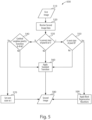
- Method 500 may start with first image 510, such as the image prior to Image 1 in FIG. 3A showing the "l” 304 and "y" 306.
- First image 510 may have a set of states for the pixels of the display, which may be stored in a display controller, such as display controller 112 in FIG. 1 .
- second image data is received, such as by display controller 112.
- the second image data may include optical states of the pixels in the display in order to display the second image, such as Image 1 in FIG. 3A displaying the letter "x.”
- method 500 proceeds to act 530. If the current state of the pixel is in neither a black (B) state nor an indication (I) state, then a standard transition used to operate the electrophoretic display is applied by act 560 in displaying the second image by act 580.
- act 540 examines the transitions of the pixel's cardinal neighbors to determine whether one or more of the cardinal neighbors is undergoing a black (B) state to white (W) state transition from the first image to the second image.
- act 540 may include determining whether a threshold number (e.g., 1, 2, 3, 4) of cardinal neighbors of the pixel transition from a black state to a white state.
- the standard transition used to operate the electrophoretic display is applied by act 560 in displaying the second image by act 580. If, by contrast, there is one or more cardinal neighbors experiencing a black state to white state transition or if the number of cardinal neighbors experiencing a black state to white state transition is above a threshold, then the state of the pixel is set to an indication (I) state by act 570 to form the second image by act 580. In this manner, the pixel is identified as potentially experiencing a blooming event by one or more of its cardinal neighbors.
- method 500 proceeds to act 550, which determines the next state of the pixel from the data of the second image. If the next state of the pixel is not the black state (e.g., white state), then the standard transition used to operate the electrophoretic display is applied by act 560 in displaying the second image by act 580. If the next state of the pixel is the black (B) state, then a black regeneration waveform, such as the one depicted in FIG. 4 , is applied to the pixel by act 590 in displaying the second image by act 580.
- a black regeneration waveform such as the one depicted in FIG. 4
- the black regeneration waveform is applied to those pixels identified as likely to have experienced a blooming event as indicated by being in the indication (I) state.
- Acts 550 and 590 may occur, for example, for pixel 308 when going from Image 1 of FIG. 3A to Image 2 of FIG. 3B .
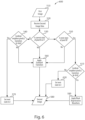
- FIG. 6 shows steps of method 600 according to another embodiment, which includes additional steps to those of method 500 shown in FIG. 5 . These additional steps provide further selection over when the black regeneration waveform is applied in act 590.
- a pixel that has a current state as an indication (I) state by act 530 and a next state as the black (B) state by act 550 proceeds to step 610 of method 600, which examines the type of transition for one or more cardinal neighbors of the pixel in transitioning to the second image.
- the black regeneration waveform is applied to the pixel by act 590 in displaying the second image by act 580.
- the black regeneration waveform is applied to the pixel. If the pixel does not meet the conditions of act 610 where there are no cardinal neighbors transitioning from a white (W) state to a black (B) state or the number of cardinal neighbors undergoing such a transition is below a threshold, then the pixel is set to the indication (I) state by act 620.
- the pixel may receive the black regeneration waveform when one or more cardinal neighbors transition to a black state to reduce the likelihood of a lighter pixel next to a darker pixel and therefore the visibility of light edge artifacts to a viewer of the displayed second image.
- FIG. 7 shows alternative steps that may be implemented in operating an electro-optic display.
- Method 7 includes additional steps to those of method 500 shown in FIG. 5 . These additional steps provide further selection over when the black regeneration waveform is applied in act 590.
- a pixel that has a current state as an indication (I) state by act 530 and a next state as the black (B) state by act 550 proceeds to step 710 of method 700, which examines the next state for one or more cardinal neighbors of the pixel in the second image. If one or more cardinal neighbors have a next state as a black (B) state, then the black regeneration waveform is applied to the pixel by act 590 in displaying the second image by act 580.
- Method 700 provides an alternative method for selectively applying the black regeneration waveform to pixels in reducing the presence of light edge artifacts in images displayed on the electro-optic display.
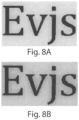
- FIG. 8A shows an example image of text displayed on an electro-optic display where such light edge correction is not used. The appearance of lighter regions in the text, particularly in the letters "v" and "j," is present.
- FIG. 8B shows an example image of the same text shown on an electro-optic display operated in a manner described herein to reduce the presence of such light edge artifacts.
Landscapes
- Physics & Mathematics (AREA)
- Engineering & Computer Science (AREA)
- General Physics & Mathematics (AREA)
- Theoretical Computer Science (AREA)
- Computer Hardware Design (AREA)
- Optics & Photonics (AREA)
- Nonlinear Science (AREA)
- Crystallography & Structural Chemistry (AREA)
- Chemical & Material Sciences (AREA)
- Ceramic Engineering (AREA)
- Control Of Indicators Other Than Cathode Ray Tubes (AREA)
- Electrochromic Elements, Electrophoresis, Or Variable Reflection Or Absorption Elements (AREA)
- Liquid Crystal Display Device Control (AREA)
Claims (5)
- Verfahren zum Betreiben einer elektrophoretischen Anzeige (101) zum Reduzieren von Lichtkantenartefakten, wobei die Anzeige (101) dazu ausgelegt ist, eine Folge von Schwarzweißbildern anzuzeigen, die ein erstes Bild (302, 304, 306), ein zweites Bild (302, 308) und ein nachfolgendes Bild (310, 312) umfassen, wobei das Verfahren die folgenden Schritte umfasst:
während eines ersten Übergangs vom ersten Bild (302, 304, 306) zum zweiten Bild:Auswählen eines ersten Pixels (308) der Anzeige (101);Detektieren eines Nullzustandsübergangs des ersten Pixels (308) von schwarz im ersten Bild zu schwarz im zweiten Bild;Bestimmen, ob die Anzahl von Hauptnachbarn des ersten Pixels (308), das von einem schwarzen Zustand im ersten Bild zu einem weißen Zustand im zweiten Bild übergeht, mindestens gleich einer ersten Schwellwertanzahl von Pixeln ist; undin Reaktion darauf, dass die Anzahl von Hauptnachbarpixeln des ersten Pixels (308), das von einem schwarzen Zustand im ersten Bild zu einem weißen Zustand im zweiten Bild übergeht, mindestens gleich der Schwellwertanzahl von Pixeln ist, Anlegen eines Spannungssignals an das erste Pixel während des zweiten Übergangs vom zweiten Bild zum nachfolgenden Bild, wobei das Spannungssignal eine Wellenform aufweist, die dazu ausgelegt ist, einen optischen schwarzen Zustand für das erste Pixel zu regenerieren. - Verfahren nach Anspruch 1, wobei in Reaktion darauf, dass der eine oder die mehreren Hauptnachbarn im nachfolgenden Bild einen schwarzen Zustand aufweisen, das Anlegen eines Spannungssignals an das erste Pixel zusätzlich ist.
- Anzeige, die Folgendes umfasst:eine elektrophoretische Anzeige undeine Ansteuerschaltung, die an die elektrooptische Anzeige gekoppelt und dazu ausgelegt ist, das Verfahren nach Anspruch 1 durchzuführen.
- Anzeige nach Anspruch 3, wobei die Schwellwertanzahl von Hauptnachbarn eins ist.
- Anzeige nach Anspruch 3, wobei die Schwellwertanzahl von Hauptnachbarn größer als eins ist.
Applications Claiming Priority (2)
| Application Number | Priority Date | Filing Date | Title |
|---|---|---|---|
| US201662292829P | 2016-02-08 | 2016-02-08 | |
| PCT/US2017/016925 WO2017139323A1 (en) | 2016-02-08 | 2017-02-08 | Methods and apparatus for operating an electro-optic display in white mode |
Publications (4)
| Publication Number | Publication Date |
|---|---|
| EP3414613A1 EP3414613A1 (de) | 2018-12-19 |
| EP3414613A4 EP3414613A4 (de) | 2019-12-18 |
| EP3414613C0 EP3414613C0 (de) | 2025-04-23 |
| EP3414613B1 true EP3414613B1 (de) | 2025-04-23 |
Family
ID=59563507
Family Applications (1)
| Application Number | Title | Priority Date | Filing Date |
|---|---|---|---|
| EP17750663.1A Active EP3414613B1 (de) | 2016-02-08 | 2017-02-08 | Verfahren und vorrichtung zum betrieb einer elektrooptischen anzeige im weissmodus |
Country Status (8)
| Country | Link |
|---|---|
| EP (1) | EP3414613B1 (de) |
| JP (2) | JP6813584B2 (de) |
| KR (1) | KR102250635B1 (de) |
| CN (3) | CN108463763B (de) |
| ES (1) | ES3029534T3 (de) |
| PL (1) | PL3414613T3 (de) |
| TW (2) | TWI715933B (de) |
| WO (1) | WO2017139323A1 (de) |
Families Citing this family (9)
| Publication number | Priority date | Publication date | Assignee | Title |
|---|---|---|---|---|
| EP3743909A4 (de) * | 2018-01-22 | 2021-08-18 | E Ink Corporation | Elektrooptische anzeigen und verfahren zur ansteuerung davon |
| US11770806B2 (en) | 2018-11-12 | 2023-09-26 | Qualcomm Incorporated | Spatial quasi co-location conflict handling |
| CN114641820B (zh) * | 2019-11-14 | 2024-01-05 | 伊英克公司 | 用于驱动电光显示器的方法 |
| US11568786B2 (en) * | 2020-05-31 | 2023-01-31 | E Ink Corporation | Electro-optic displays, and methods for driving same |
| KR102720288B1 (ko) * | 2020-06-11 | 2024-10-21 | 이 잉크 코포레이션 | 전기 광학 디스플레이들, 및 이를 구동하기 위한 방법들 |
| CN112215816B (zh) * | 2020-10-13 | 2024-01-30 | 四川极速智能科技有限公司 | 一种生产线中显示器故障的实时检测方法、存储介质和装置 |
| CN114863882B (zh) * | 2021-01-20 | 2024-06-25 | 广州视源电子科技股份有限公司 | 电子墨水屏的刷新方法及装置 |
| CA3228148A1 (en) * | 2021-09-06 | 2023-03-09 | E Ink Corporation | Method for driving electrophoretic display device |
| CN116805478B (zh) * | 2023-08-21 | 2023-11-14 | 惠科股份有限公司 | 电子纸显示装置的驱动方法和电子设备 |
Family Cites Families (127)
| Publication number | Priority date | Publication date | Assignee | Title |
|---|---|---|---|---|
| US4418346A (en) | 1981-05-20 | 1983-11-29 | Batchelder J Samuel | Method and apparatus for providing a dielectrophoretic display of visual information |
| US5745094A (en) | 1994-12-28 | 1998-04-28 | International Business Machines Corporation | Electrophoretic display |
| US6137467A (en) | 1995-01-03 | 2000-10-24 | Xerox Corporation | Optically sensitive electric paper |
| US7956841B2 (en) | 1995-07-20 | 2011-06-07 | E Ink Corporation | Stylus-based addressing structures for displays |
| US7327511B2 (en) | 2004-03-23 | 2008-02-05 | E Ink Corporation | Light modulators |
| US7583251B2 (en) | 1995-07-20 | 2009-09-01 | E Ink Corporation | Dielectrophoretic displays |
| US8139050B2 (en) | 1995-07-20 | 2012-03-20 | E Ink Corporation | Addressing schemes for electronic displays |
| US7999787B2 (en) | 1995-07-20 | 2011-08-16 | E Ink Corporation | Methods for driving electrophoretic displays using dielectrophoretic forces |
| US7193625B2 (en) | 1999-04-30 | 2007-03-20 | E Ink Corporation | Methods for driving electro-optic displays, and apparatus for use therein |
| US8089453B2 (en) | 1995-07-20 | 2012-01-03 | E Ink Corporation | Stylus-based addressing structures for displays |
| US6866760B2 (en) | 1998-08-27 | 2005-03-15 | E Ink Corporation | Electrophoretic medium and process for the production thereof |
| US7411719B2 (en) | 1995-07-20 | 2008-08-12 | E Ink Corporation | Electrophoretic medium and process for the production thereof |
| US7259744B2 (en) | 1995-07-20 | 2007-08-21 | E Ink Corporation | Dielectrophoretic displays |
| US7023420B2 (en) | 2000-11-29 | 2006-04-04 | E Ink Corporation | Electronic display with photo-addressing means |
| US5760761A (en) | 1995-12-15 | 1998-06-02 | Xerox Corporation | Highlight color twisting ball display |
| US6055091A (en) | 1996-06-27 | 2000-04-25 | Xerox Corporation | Twisting-cylinder display |
| US5808783A (en) | 1996-06-27 | 1998-09-15 | Xerox Corporation | High reflectance gyricon display |
| US5930026A (en) | 1996-10-25 | 1999-07-27 | Massachusetts Institute Of Technology | Nonemissive displays and piezoelectric power supplies therefor |
| US5777782A (en) | 1996-12-24 | 1998-07-07 | Xerox Corporation | Auxiliary optics for a twisting ball display |
| DE69830566T2 (de) | 1997-02-06 | 2006-05-11 | University College Dublin | Elektrochromes system |
| US7002728B2 (en) | 1997-08-28 | 2006-02-21 | E Ink Corporation | Electrophoretic particles, and processes for the production thereof |
| US6054071A (en) | 1998-01-28 | 2000-04-25 | Xerox Corporation | Poled electrets for gyricon-based electric-paper displays |
| US6753999B2 (en) | 1998-03-18 | 2004-06-22 | E Ink Corporation | Electrophoretic displays in portable devices and systems for addressing such displays |
| AU3190499A (en) | 1998-03-18 | 1999-10-11 | E-Ink Corporation | Electrophoretic displays and systems for addressing such displays |
| US7075502B1 (en) | 1998-04-10 | 2006-07-11 | E Ink Corporation | Full color reflective display with multichromatic sub-pixels |
| WO1999056171A1 (en) | 1998-04-27 | 1999-11-04 | E-Ink Corporation | Shutter mode microencapsulated electrophoretic display |
| US6241921B1 (en) | 1998-05-15 | 2001-06-05 | Massachusetts Institute Of Technology | Heterogeneous display elements and methods for their fabrication |
| US20030102858A1 (en) | 1998-07-08 | 2003-06-05 | E Ink Corporation | Method and apparatus for determining properties of an electrophoretic display |
| WO2000003349A1 (en) | 1998-07-08 | 2000-01-20 | E Ink Corporation | Method and apparatus for sensing the state of an electrophoretic display |
| US6144361A (en) | 1998-09-16 | 2000-11-07 | International Business Machines Corporation | Transmissive electrophoretic display with vertical electrodes |
| US6184856B1 (en) | 1998-09-16 | 2001-02-06 | International Business Machines Corporation | Transmissive electrophoretic display with laterally adjacent color cells |
| US6225971B1 (en) | 1998-09-16 | 2001-05-01 | International Business Machines Corporation | Reflective electrophoretic display with laterally adjacent color cells using an absorbing panel |
| US6271823B1 (en) | 1998-09-16 | 2001-08-07 | International Business Machines Corporation | Reflective electrophoretic display with laterally adjacent color cells using a reflective panel |
| US6128124A (en) | 1998-10-16 | 2000-10-03 | Xerox Corporation | Additive color electric paper without registration or alignment of individual elements |
| US6147791A (en) | 1998-11-25 | 2000-11-14 | Xerox Corporation | Gyricon displays utilizing rotating elements and magnetic latching |
| US6097531A (en) | 1998-11-25 | 2000-08-01 | Xerox Corporation | Method of making uniformly magnetized elements for a gyricon display |
| US6504524B1 (en) | 2000-03-08 | 2003-01-07 | E Ink Corporation | Addressing methods for displays having zero time-average field |
| US7119772B2 (en) | 1999-04-30 | 2006-10-10 | E Ink Corporation | Methods for driving bistable electro-optic displays, and apparatus for use therein |
| US6531997B1 (en) | 1999-04-30 | 2003-03-11 | E Ink Corporation | Methods for addressing electrophoretic displays |
| US7012600B2 (en) | 1999-04-30 | 2006-03-14 | E Ink Corporation | Methods for driving bistable electro-optic displays, and apparatus for use therein |
| US8009348B2 (en) | 1999-05-03 | 2011-08-30 | E Ink Corporation | Machine-readable displays |
| HK1047623B (en) | 1999-10-11 | 2005-05-06 | University College Dublin | Electrochromic device |
| US6672921B1 (en) | 2000-03-03 | 2004-01-06 | Sipix Imaging, Inc. | Manufacturing process for electrophoretic display |
| US6788449B2 (en) | 2000-03-03 | 2004-09-07 | Sipix Imaging, Inc. | Electrophoretic display and novel process for its manufacture |
| AU2002250304A1 (en) | 2001-03-13 | 2002-09-24 | E Ink Corporation | Apparatus for displaying drawings |
| US7679814B2 (en) | 2001-04-02 | 2010-03-16 | E Ink Corporation | Materials for use in electrophoretic displays |
| EP1666964B1 (de) | 2001-04-02 | 2018-12-19 | E Ink Corporation | Elektrophoretisches Medium mit verbesserter Bildstabilität |
| US7535624B2 (en) | 2001-07-09 | 2009-05-19 | E Ink Corporation | Electro-optic display and materials for use therein |
| US6982178B2 (en) | 2002-06-10 | 2006-01-03 | E Ink Corporation | Components and methods for use in electro-optic displays |
| US6825970B2 (en) | 2001-09-14 | 2004-11-30 | E Ink Corporation | Methods for addressing electro-optic materials |
| US8125501B2 (en) | 2001-11-20 | 2012-02-28 | E Ink Corporation | Voltage modulated driver circuits for electro-optic displays |
| US7202847B2 (en) | 2002-06-28 | 2007-04-10 | E Ink Corporation | Voltage modulated driver circuits for electro-optic displays |
| US7952557B2 (en) | 2001-11-20 | 2011-05-31 | E Ink Corporation | Methods and apparatus for driving electro-optic displays |
| US7528822B2 (en) | 2001-11-20 | 2009-05-05 | E Ink Corporation | Methods for driving electro-optic displays |
| US8558783B2 (en) * | 2001-11-20 | 2013-10-15 | E Ink Corporation | Electro-optic displays with reduced remnant voltage |
| US9412314B2 (en) | 2001-11-20 | 2016-08-09 | E Ink Corporation | Methods for driving electro-optic displays |
| US8593396B2 (en) * | 2001-11-20 | 2013-11-26 | E Ink Corporation | Methods and apparatus for driving electro-optic displays |
| US6900851B2 (en) | 2002-02-08 | 2005-05-31 | E Ink Corporation | Electro-optic displays and optical systems for addressing such displays |
| CN100339757C (zh) | 2002-03-06 | 2007-09-26 | 株式会社普利司通 | 图像显示装置和方法 |
| US6950220B2 (en) | 2002-03-18 | 2005-09-27 | E Ink Corporation | Electro-optic displays, and methods for driving same |
| WO2003092077A2 (en) | 2002-04-24 | 2003-11-06 | E Ink Corporation | Electronic displays |
| US7110164B2 (en) | 2002-06-10 | 2006-09-19 | E Ink Corporation | Electro-optic displays, and processes for the production thereof |
| US20080024482A1 (en) | 2002-06-13 | 2008-01-31 | E Ink Corporation | Methods for driving electro-optic displays |
| US7839564B2 (en) | 2002-09-03 | 2010-11-23 | E Ink Corporation | Components and methods for use in electro-optic displays |
| JP2006510066A (ja) | 2002-12-16 | 2006-03-23 | イー−インク コーポレイション | 電気光学表示装置用バックプレーン |
| US6922276B2 (en) | 2002-12-23 | 2005-07-26 | E Ink Corporation | Flexible electro-optic displays |
| US7339715B2 (en) | 2003-03-25 | 2008-03-04 | E Ink Corporation | Processes for the production of electrophoretic displays |
| US9672766B2 (en) | 2003-03-31 | 2017-06-06 | E Ink Corporation | Methods for driving electro-optic displays |
| US7236291B2 (en) | 2003-04-02 | 2007-06-26 | Bridgestone Corporation | Particle use for image display media, image display panel using the particles, and image display device |
| US8174490B2 (en) | 2003-06-30 | 2012-05-08 | E Ink Corporation | Methods for driving electrophoretic displays |
| EP1656658A4 (de) | 2003-08-19 | 2009-12-30 | E Ink Corp | Verfahren zur steuerung von elektrooptischen displays |
| US7839381B2 (en) * | 2003-09-08 | 2010-11-23 | Koninklijke Philips Electronics N.V. | Driving method for an electrophoretic display with accurate greyscale and minimized average power consumption |
| WO2005029458A1 (en) | 2003-09-19 | 2005-03-31 | E Ink Corporation | Methods for reducing edge effects in electro-optic displays |
| US8300006B2 (en) | 2003-10-03 | 2012-10-30 | E Ink Corporation | Electrophoretic display unit |
| US8319759B2 (en) | 2003-10-08 | 2012-11-27 | E Ink Corporation | Electrowetting displays |
| US7420549B2 (en) | 2003-10-08 | 2008-09-02 | E Ink Corporation | Electro-wetting displays |
| EP1687801A1 (de) * | 2003-11-21 | 2006-08-09 | Koninklijke Philips Electronics N.V. | Verfahren und vorrichtung zur ansteuerung einer elektrophoretischen anzeigeeinrichtung mit verringerter bildretention |
| US20070091117A1 (en) * | 2003-11-21 | 2007-04-26 | Koninklijke Philips Electronics N.V. | Electrophoretic display device and a method and apparatus for improving image quality in an electrophoretic display device |
| WO2005052905A1 (en) | 2003-11-25 | 2005-06-09 | Koninklijke Philips Electronics N.V. | A display apparatus with a display device and a cyclic rail-stabilized method of driving the display device |
| US8928562B2 (en) | 2003-11-25 | 2015-01-06 | E Ink Corporation | Electro-optic displays, and methods for driving same |
| CN1926601B (zh) * | 2004-03-01 | 2010-11-17 | 皇家飞利浦电子股份有限公司 | 在电泳显示器的灰度级与单色寻址之间的转换 |
| US7492339B2 (en) | 2004-03-26 | 2009-02-17 | E Ink Corporation | Methods for driving bistable electro-optic displays |
| US7719536B2 (en) * | 2004-03-31 | 2010-05-18 | Adobe Systems Incorporated | Glyph adjustment in high resolution raster while rendering |
| US8289250B2 (en) | 2004-03-31 | 2012-10-16 | E Ink Corporation | Methods for driving electro-optic displays |
| US20050253777A1 (en) | 2004-05-12 | 2005-11-17 | E Ink Corporation | Tiled displays and methods for driving same |
| US20080136774A1 (en) | 2004-07-27 | 2008-06-12 | E Ink Corporation | Methods for driving electrophoretic displays using dielectrophoretic forces |
| CN1989541A (zh) * | 2004-07-27 | 2007-06-27 | 皇家飞利浦电子股份有限公司 | 驱动电泳显示器 |
| WO2006015044A1 (en) | 2004-07-27 | 2006-02-09 | E Ink Corporation | Electro-optic displays |
| US7453445B2 (en) | 2004-08-13 | 2008-11-18 | E Ink Corproation | Methods for driving electro-optic displays |
| WO2006064459A2 (en) * | 2004-12-17 | 2006-06-22 | Koninklijke Philips Electronics N.V. | Gamma correction in a bi-stable display |
| JP4718859B2 (ja) | 2005-02-17 | 2011-07-06 | セイコーエプソン株式会社 | 電気泳動装置とその駆動方法、及び電子機器 |
| JP4690079B2 (ja) | 2005-03-04 | 2011-06-01 | セイコーエプソン株式会社 | 電気泳動装置とその駆動方法、及び電子機器 |
| CN100456118C (zh) * | 2005-03-29 | 2009-01-28 | 精工爱普生株式会社 | 电泳显示装置 |
| JP5092223B2 (ja) * | 2005-10-04 | 2012-12-05 | パナソニック株式会社 | 画像処理装置 |
| US20080024429A1 (en) | 2006-07-25 | 2008-01-31 | E Ink Corporation | Electrophoretic displays using gaseous fluids |
| CN101681211A (zh) | 2007-05-21 | 2010-03-24 | 伊英克公司 | 用于驱动视频电光显示器的方法 |
| US8355018B2 (en) * | 2007-06-15 | 2013-01-15 | Ricoh Co., Ltd. | Independent pixel waveforms for updating electronic paper displays |
| US8130192B2 (en) * | 2007-06-15 | 2012-03-06 | Ricoh Co., Ltd. | Method for reducing image artifacts on electronic paper displays |
| JP5157322B2 (ja) * | 2007-08-30 | 2013-03-06 | セイコーエプソン株式会社 | 電気泳動表示装置、電気泳動表示装置の駆動方法、及び電子機器 |
| US8314784B2 (en) | 2008-04-11 | 2012-11-20 | E Ink Corporation | Methods for driving electro-optic displays |
| US8310440B2 (en) * | 2008-11-10 | 2012-11-13 | Seiko Epson Corporation | Method of driving electrophoretic display device, electrophoretic display device, and electronic apparatus |
| TWI406217B (zh) * | 2008-12-29 | 2013-08-21 | Prime View Int Co Ltd | 電泳式顯示裝置的顯示方法及運用此方法之電泳式顯示裝置 |
| US8237733B2 (en) * | 2009-03-31 | 2012-08-07 | Ricoh Co., Ltd. | Page transition on electronic paper display |
| WO2010147041A1 (ja) * | 2009-06-16 | 2010-12-23 | コニカミノルタホールディングス株式会社 | メモリ性表示デバイス及びメモリ性表示デバイスシステム |
| WO2011003446A1 (en) | 2009-07-08 | 2011-01-13 | Cimteclab S.R.L. | Synthesis of novel multifunctional cardanol's derivatives and their use as halogen free polyurethanic foams precursors |
| KR101136312B1 (ko) * | 2009-12-31 | 2012-04-20 | 삼성전자주식회사 | Epd 구동 방법 및 장치 |
| CN102834857B (zh) | 2010-04-09 | 2016-03-02 | 伊英克公司 | 用于驱动电光显示器的方法 |
| JP5740831B2 (ja) * | 2010-04-12 | 2015-07-01 | セイコーエプソン株式会社 | 電気泳動表示装置の駆動方法、電気泳動表示装置及び電子機器 |
| JP2012008209A (ja) * | 2010-06-22 | 2012-01-12 | Seiko Epson Corp | 表示シート、表示装置、電子機器および表示シートの駆動方法 |
| US8665206B2 (en) * | 2010-08-10 | 2014-03-04 | Sipix Imaging, Inc. | Driving method to neutralize grey level shift for electrophoretic displays |
| CN102376263B (zh) * | 2010-08-19 | 2014-11-19 | 上海天马微电子有限公司 | 电子纸的驱动方法及驱动装置 |
| JP5691302B2 (ja) * | 2010-08-31 | 2015-04-01 | セイコーエプソン株式会社 | 制御装置、表示装置及び表示装置の制御方法 |
| CN102456320A (zh) * | 2010-10-19 | 2012-05-16 | 天钰科技股份有限公司 | 电泳显示器及其画面更新方法 |
| US9349327B2 (en) | 2010-12-06 | 2016-05-24 | Lg Display Co., Ltd. | Electrophoretic display apparatus, method for driving same, and method for measuring image stability thereof |
| CN103403615A (zh) * | 2011-02-08 | 2013-11-20 | 精工爱普生株式会社 | 电泳显示控制器中的自动波形连接 |
| JP5919639B2 (ja) * | 2011-04-15 | 2016-05-18 | セイコーエプソン株式会社 | 電気泳動表示装置の制御方法、電気泳動表示装置の制御装置、電気泳動表示装置、及び電子機器 |
| JP2012237960A (ja) * | 2011-05-10 | 2012-12-06 | Seiko Epson Corp | 電気光学装置の制御方法、電気光学装置の制御装置、電気光学装置、及び電子機器 |
| CN102262864A (zh) * | 2011-08-30 | 2011-11-30 | 福建华映显示科技有限公司 | 可改善残影的电泳显示器及其画面更新方法 |
| US20130069968A1 (en) * | 2011-09-16 | 2013-03-21 | Qualcomm Mems Technologies, Inc. | Methods and apparatus for hybrid halftoning of an image |
| EP3783597A1 (de) * | 2012-02-01 | 2021-02-24 | E Ink Corporation | Verfahren zur ansteuerung elektrooptischer anzeigen |
| JP5994276B2 (ja) * | 2012-02-16 | 2016-09-21 | セイコーエプソン株式会社 | 画像処理装置、表示装置および画像処理方法 |
| JP6256822B2 (ja) * | 2012-09-14 | 2018-01-10 | Tianma Japan株式会社 | 電気泳動表示装置及びその駆動方法 |
| WO2014134504A1 (en) | 2013-03-01 | 2014-09-04 | E Ink Corporation | Methods for driving electro-optic displays |
| CN103247268A (zh) * | 2013-03-07 | 2013-08-14 | 北京君正集成电路股份有限公司 | 一种消除残影的方法及装置 |
| EP4156165A3 (de) | 2013-07-31 | 2023-06-21 | E Ink Corporation | Verfahren zur ansteuerung elektrooptischer anzeigen |
| GB2519777B (en) * | 2013-10-30 | 2020-06-17 | Flexenable Ltd | Display systems and methods |
| PL3254275T3 (pl) * | 2015-02-04 | 2023-10-02 | E Ink Corporation | Wyświetlacze elektrooptyczne wyświetlające w trybie ciemnym i w trybie jasnym oraz powiązane urządzenie i sposoby |
-
2017
- 2017-02-08 WO PCT/US2017/016925 patent/WO2017139323A1/en not_active Ceased
- 2017-02-08 CN CN201780005835.8A patent/CN108463763B/zh active Active
- 2017-02-08 JP JP2018540760A patent/JP6813584B2/ja active Active
- 2017-02-08 TW TW108105560A patent/TWI715933B/zh active
- 2017-02-08 CN CN202010668158.1A patent/CN111722396B/zh active Active
- 2017-02-08 TW TW106104338A patent/TWI658312B/zh active
- 2017-02-08 EP EP17750663.1A patent/EP3414613B1/de active Active
- 2017-02-08 PL PL17750663.1T patent/PL3414613T3/pl unknown
- 2017-02-08 KR KR1020187021929A patent/KR102250635B1/ko active Active
- 2017-02-08 CN CN202210367820.9A patent/CN114613312A/zh active Pending
- 2017-02-08 ES ES17750663T patent/ES3029534T3/es active Active
-
2020
- 2020-10-21 JP JP2020176466A patent/JP2021006935A/ja not_active Withdrawn
Also Published As
| Publication number | Publication date |
|---|---|
| HK1252982A1 (zh) | 2019-06-06 |
| KR20180089551A (ko) | 2018-08-08 |
| TWI658312B (zh) | 2019-05-01 |
| JP2019505847A (ja) | 2019-02-28 |
| JP6813584B2 (ja) | 2021-01-13 |
| TW201921072A (zh) | 2019-06-01 |
| CN111722396B (zh) | 2023-11-07 |
| TWI715933B (zh) | 2021-01-11 |
| JP2021006935A (ja) | 2021-01-21 |
| PL3414613T3 (pl) | 2025-08-18 |
| WO2017139323A1 (en) | 2017-08-17 |
| TW201741751A (zh) | 2017-12-01 |
| KR102250635B1 (ko) | 2021-05-10 |
| EP3414613A4 (de) | 2019-12-18 |
| CN114613312A (zh) | 2022-06-10 |
| CN108463763B (zh) | 2022-05-06 |
| EP3414613C0 (de) | 2025-04-23 |
| CN111722396A (zh) | 2020-09-29 |
| EP3414613A1 (de) | 2018-12-19 |
| CN108463763A (zh) | 2018-08-28 |
| ES3029534T3 (en) | 2025-06-24 |
Similar Documents
| Publication | Publication Date | Title |
|---|---|---|
| EP3414613B1 (de) | Verfahren und vorrichtung zum betrieb einer elektrooptischen anzeige im weissmodus | |
| US11030936B2 (en) | Methods and apparatus for operating an electro-optic display in white mode | |
| EP3028269B1 (de) | Verfahren zur ansteuerung elektrooptischer anzeigen | |
| US11935496B2 (en) | Electro-optic displays, and methods for driving same | |
| EP3682440B1 (de) | Verfahren zur ansteuerung von elektrooptischen anzeigen | |
| US12322353B2 (en) | Electro-optic displays and driving methods | |
| US12609067B2 (en) | Electro-optic displays, and methods for driving same | |
| CA3054848C (en) | Electro-optic displays and driving methods | |
| WO2019144097A1 (en) | Electro-optic displays, and methods for driving same | |
| HK40066715A (zh) | 用於在白色模式下操作电光显示器的方法和设备 | |
| HK40028120A (en) | Methods and apparatus for operating an electro-optic display in white mode | |
| HK40028120B (zh) | 用於在白色模式下操作电光显示器的方法和设备 | |
| HK1252982B (zh) | 用於在白色模式下操作电光显示器的方法和设备 |
Legal Events
| Date | Code | Title | Description |
|---|---|---|---|
| STAA | Information on the status of an ep patent application or granted ep patent |
Free format text: STATUS: THE INTERNATIONAL PUBLICATION HAS BEEN MADE |
|
| PUAI | Public reference made under article 153(3) epc to a published international application that has entered the european phase |
Free format text: ORIGINAL CODE: 0009012 |
|
| STAA | Information on the status of an ep patent application or granted ep patent |
Free format text: STATUS: REQUEST FOR EXAMINATION WAS MADE |
|
| 17P | Request for examination filed |
Effective date: 20180910 |
|
| AK | Designated contracting states |
Kind code of ref document: A1 Designated state(s): AL AT BE BG CH CY CZ DE DK EE ES FI FR GB GR HR HU IE IS IT LI LT LU LV MC MK MT NL NO PL PT RO RS SE SI SK SM TR |
|
| AX | Request for extension of the european patent |
Extension state: BA ME |
|
| DAV | Request for validation of the european patent (deleted) | ||
| DAX | Request for extension of the european patent (deleted) | ||
| RIC1 | Information provided on ipc code assigned before grant |
Ipc: G09G 3/20 20060101ALI20190805BHEP Ipc: G09G 3/34 20060101ALI20190805BHEP Ipc: G02B 26/02 20060101AFI20190805BHEP Ipc: G02F 1/03 20060101ALI20190805BHEP Ipc: G09G 3/36 20060101ALI20190805BHEP |
|
| A4 | Supplementary search report drawn up and despatched |
Effective date: 20191115 |
|
| RIC1 | Information provided on ipc code assigned before grant |
Ipc: G09G 3/34 20060101ALI20191111BHEP Ipc: G02B 26/02 20060101AFI20191111BHEP Ipc: G02F 1/03 20060101ALI20191111BHEP Ipc: G09G 3/36 20060101ALI20191111BHEP Ipc: G09G 3/20 20060101ALI20191111BHEP |
|
| STAA | Information on the status of an ep patent application or granted ep patent |
Free format text: STATUS: EXAMINATION IS IN PROGRESS |
|
| 17Q | First examination report despatched |
Effective date: 20211005 |
|
| GRAP | Despatch of communication of intention to grant a patent |
Free format text: ORIGINAL CODE: EPIDOSNIGR1 |
|
| STAA | Information on the status of an ep patent application or granted ep patent |
Free format text: STATUS: GRANT OF PATENT IS INTENDED |
|
| RIN1 | Information on inventor provided before grant (corrected) |
Inventor name: CROUNSE, KENNETH R. Inventor name: EMELIE, PIERRE-YVES |
|
| INTG | Intention to grant announced |
Effective date: 20250210 |
|
| GRAS | Grant fee paid |
Free format text: ORIGINAL CODE: EPIDOSNIGR3 |
|
| GRAA | (expected) grant |
Free format text: ORIGINAL CODE: 0009210 |
|
| STAA | Information on the status of an ep patent application or granted ep patent |
Free format text: STATUS: THE PATENT HAS BEEN GRANTED |
|
| AK | Designated contracting states |
Kind code of ref document: B1 Designated state(s): AL AT BE BG CH CY CZ DE DK EE ES FI FR GB GR HR HU IE IS IT LI LT LU LV MC MK MT NL NO PL PT RO RS SE SI SK SM TR |
|
| REG | Reference to a national code |
Ref country code: GB Ref legal event code: FG4D |
|
| REG | Reference to a national code |
Ref country code: CH Ref legal event code: EP |
|
| REG | Reference to a national code |
Ref country code: IE Ref legal event code: FG4D |
|
| U01 | Request for unitary effect filed |
Effective date: 20250423 |
|
| U07 | Unitary effect registered |
Designated state(s): AT BE BG DE DK EE FI FR IT LT LU LV MT NL PT RO SE SI Effective date: 20250429 |
|
| REG | Reference to a national code |
Ref country code: ES Ref legal event code: FG2A Ref document number: 3029534 Country of ref document: ES Kind code of ref document: T3 Effective date: 20250624 |
|
| PG25 | Lapsed in a contracting state [announced via postgrant information from national office to epo] |
Ref country code: GR Free format text: LAPSE BECAUSE OF FAILURE TO SUBMIT A TRANSLATION OF THE DESCRIPTION OR TO PAY THE FEE WITHIN THE PRESCRIBED TIME-LIMIT Effective date: 20250724 |
|
| PG25 | Lapsed in a contracting state [announced via postgrant information from national office to epo] |
Ref country code: HR Free format text: LAPSE BECAUSE OF FAILURE TO SUBMIT A TRANSLATION OF THE DESCRIPTION OR TO PAY THE FEE WITHIN THE PRESCRIBED TIME-LIMIT Effective date: 20250423 |
|
| PG25 | Lapsed in a contracting state [announced via postgrant information from national office to epo] |
Ref country code: RS Free format text: LAPSE BECAUSE OF FAILURE TO SUBMIT A TRANSLATION OF THE DESCRIPTION OR TO PAY THE FEE WITHIN THE PRESCRIBED TIME-LIMIT Effective date: 20250723 |
|
| PG25 | Lapsed in a contracting state [announced via postgrant information from national office to epo] |
Ref country code: IS Free format text: LAPSE BECAUSE OF FAILURE TO SUBMIT A TRANSLATION OF THE DESCRIPTION OR TO PAY THE FEE WITHIN THE PRESCRIBED TIME-LIMIT Effective date: 20250823 |
|
| PG25 | Lapsed in a contracting state [announced via postgrant information from national office to epo] |
Ref country code: SM Free format text: LAPSE BECAUSE OF FAILURE TO SUBMIT A TRANSLATION OF THE DESCRIPTION OR TO PAY THE FEE WITHIN THE PRESCRIBED TIME-LIMIT Effective date: 20250423 |
|
| PG25 | Lapsed in a contracting state [announced via postgrant information from national office to epo] |
Ref country code: CZ Free format text: LAPSE BECAUSE OF FAILURE TO SUBMIT A TRANSLATION OF THE DESCRIPTION OR TO PAY THE FEE WITHIN THE PRESCRIBED TIME-LIMIT Effective date: 20250423 |
|
| PG25 | Lapsed in a contracting state [announced via postgrant information from national office to epo] |
Ref country code: SK Free format text: LAPSE BECAUSE OF FAILURE TO SUBMIT A TRANSLATION OF THE DESCRIPTION OR TO PAY THE FEE WITHIN THE PRESCRIBED TIME-LIMIT Effective date: 20250423 |
|
| U20 | Renewal fee for the european patent with unitary effect paid |
Year of fee payment: 10 Effective date: 20260121 |
|
| PLBE | No opposition filed within time limit |
Free format text: ORIGINAL CODE: 0009261 |
|
| STAA | Information on the status of an ep patent application or granted ep patent |
Free format text: STATUS: NO OPPOSITION FILED WITHIN TIME LIMIT |
|
| REG | Reference to a national code |
Ref country code: CH Ref legal event code: U11 Free format text: ST27 STATUS EVENT CODE: U-0-0-U10-U11 (AS PROVIDED BY THE NATIONAL OFFICE) Effective date: 20260301 |
|
| REG | Reference to a national code |
Ref country code: CH Ref legal event code: L10 Free format text: ST27 STATUS EVENT CODE: U-0-0-L10-L00 (AS PROVIDED BY THE NATIONAL OFFICE) Effective date: 20260304 |
|
| 26N | No opposition filed |
Effective date: 20260126 |
|
| PGFP | Annual fee paid to national office [announced via postgrant information from national office to epo] |
Ref country code: GB Payment date: 20260121 Year of fee payment: 10 |
|
| PGFP | Annual fee paid to national office [announced via postgrant information from national office to epo] |
Ref country code: ES Payment date: 20260302 Year of fee payment: 10 |
|
| PGFP | Annual fee paid to national office [announced via postgrant information from national office to epo] |
Ref country code: NO Payment date: 20260123 Year of fee payment: 10 |
|
| PGFP | Annual fee paid to national office [announced via postgrant information from national office to epo] |
Ref country code: CH Payment date: 20260301 Year of fee payment: 10 |
|
| PGFP | Annual fee paid to national office [announced via postgrant information from national office to epo] |
Ref country code: PL Payment date: 20260123 Year of fee payment: 10 |