EP3414979B1 - Elektrische leiterplatte mit integriertem akustischem kanal - Google Patents
Elektrische leiterplatte mit integriertem akustischem kanal Download PDFInfo
- Publication number
- EP3414979B1 EP3414979B1 EP17703892.4A EP17703892A EP3414979B1 EP 3414979 B1 EP3414979 B1 EP 3414979B1 EP 17703892 A EP17703892 A EP 17703892A EP 3414979 B1 EP3414979 B1 EP 3414979B1
- Authority
- EP
- European Patent Office
- Prior art keywords
- layer
- channel
- acoustic
- circuit board
- layers
- Prior art date
- Legal status (The legal status is an assumption and is not a legal conclusion. Google has not performed a legal analysis and makes no representation as to the accuracy of the status listed.)
- Active
Links
Images


Classifications
-
- H—ELECTRICITY
- H04—ELECTRIC COMMUNICATION TECHNIQUE
- H04R—LOUDSPEAKERS, MICROPHONES, GRAMOPHONE PICK-UPS OR LIKE ACOUSTIC ELECTROMECHANICAL TRANSDUCERS; ELECTRIC HEARING AIDS; PUBLIC ADDRESS SYSTEMS
- H04R1/00—Details of transducers, loudspeakers or microphones
- H04R1/10—Earpieces; Attachments therefor ; Earphones; Monophonic headphones
- H04R1/1016—Earpieces of the intra-aural type
-
- H—ELECTRICITY
- H04—ELECTRIC COMMUNICATION TECHNIQUE
- H04R—LOUDSPEAKERS, MICROPHONES, GRAMOPHONE PICK-UPS OR LIKE ACOUSTIC ELECTROMECHANICAL TRANSDUCERS; ELECTRIC HEARING AIDS; PUBLIC ADDRESS SYSTEMS
- H04R1/00—Details of transducers, loudspeakers or microphones
- H04R1/10—Earpieces; Attachments therefor ; Earphones; Monophonic headphones
- H04R1/1091—Details not provided for in groups H04R1/1008 - H04R1/1083
-
- H—ELECTRICITY
- H04—ELECTRIC COMMUNICATION TECHNIQUE
- H04R—LOUDSPEAKERS, MICROPHONES, GRAMOPHONE PICK-UPS OR LIKE ACOUSTIC ELECTROMECHANICAL TRANSDUCERS; ELECTRIC HEARING AIDS; PUBLIC ADDRESS SYSTEMS
- H04R1/00—Details of transducers, loudspeakers or microphones
- H04R1/20—Arrangements for obtaining desired frequency or directional characteristics
- H04R1/22—Arrangements for obtaining desired frequency or directional characteristics for obtaining desired frequency characteristic only
- H04R1/28—Transducer mountings or enclosures modified by provision of mechanical or acoustic impedances, e.g. resonator, damping means
- H04R1/2807—Enclosures comprising vibrating or resonating arrangements
- H04R1/2815—Enclosures comprising vibrating or resonating arrangements of the bass reflex type
- H04R1/2823—Vents, i.e. ports, e.g. shape thereof or tuning thereof with damping material
- H04R1/2826—Vents, i.e. ports, e.g. shape thereof or tuning thereof with damping material for loudspeaker transducers
-
- H—ELECTRICITY
- H04—ELECTRIC COMMUNICATION TECHNIQUE
- H04R—LOUDSPEAKERS, MICROPHONES, GRAMOPHONE PICK-UPS OR LIKE ACOUSTIC ELECTROMECHANICAL TRANSDUCERS; ELECTRIC HEARING AIDS; PUBLIC ADDRESS SYSTEMS
- H04R5/00—Stereophonic arrangements
- H04R5/033—Headphones for stereophonic communication
-
- H—ELECTRICITY
- H05—ELECTRIC TECHNIQUES NOT OTHERWISE PROVIDED FOR
- H05K—PRINTED CIRCUITS; CASINGS OR CONSTRUCTIONAL DETAILS OF ELECTRIC APPARATUS; MANUFACTURE OF ASSEMBLAGES OF ELECTRICAL COMPONENTS
- H05K1/00—Printed circuits
- H05K1/02—Details
- H05K1/0272—Adaptations for fluid transport, e.g. channels, holes
-
- H—ELECTRICITY
- H05—ELECTRIC TECHNIQUES NOT OTHERWISE PROVIDED FOR
- H05K—PRINTED CIRCUITS; CASINGS OR CONSTRUCTIONAL DETAILS OF ELECTRIC APPARATUS; MANUFACTURE OF ASSEMBLAGES OF ELECTRICAL COMPONENTS
- H05K1/00—Printed circuits
- H05K1/02—Details
- H05K1/0277—Bendability or stretchability details
- H05K1/028—Bending or folding regions of flexible printed circuits
-
- H—ELECTRICITY
- H05—ELECTRIC TECHNIQUES NOT OTHERWISE PROVIDED FOR
- H05K—PRINTED CIRCUITS; CASINGS OR CONSTRUCTIONAL DETAILS OF ELECTRIC APPARATUS; MANUFACTURE OF ASSEMBLAGES OF ELECTRICAL COMPONENTS
- H05K1/00—Printed circuits
- H05K1/02—Details
- H05K1/0296—Conductive pattern lay-out details not covered by sub groups H05K1/02 - H05K1/0295
- H05K1/0298—Multilayer circuits
-
- H—ELECTRICITY
- H04—ELECTRIC COMMUNICATION TECHNIQUE
- H04R—LOUDSPEAKERS, MICROPHONES, GRAMOPHONE PICK-UPS OR LIKE ACOUSTIC ELECTROMECHANICAL TRANSDUCERS; ELECTRIC HEARING AIDS; PUBLIC ADDRESS SYSTEMS
- H04R1/00—Details of transducers, loudspeakers or microphones
- H04R1/20—Arrangements for obtaining desired frequency or directional characteristics
- H04R1/22—Arrangements for obtaining desired frequency or directional characteristics for obtaining desired frequency characteristic only
- H04R1/28—Transducer mountings or enclosures modified by provision of mechanical or acoustic impedances, e.g. resonator, damping means
- H04R1/2807—Enclosures comprising vibrating or resonating arrangements
- H04R1/2815—Enclosures comprising vibrating or resonating arrangements of the bass reflex type
- H04R1/2819—Enclosures comprising vibrating or resonating arrangements of the bass reflex type for loudspeaker transducers
-
- H—ELECTRICITY
- H05—ELECTRIC TECHNIQUES NOT OTHERWISE PROVIDED FOR
- H05K—PRINTED CIRCUITS; CASINGS OR CONSTRUCTIONAL DETAILS OF ELECTRIC APPARATUS; MANUFACTURE OF ASSEMBLAGES OF ELECTRICAL COMPONENTS
- H05K2201/00—Indexing scheme relating to printed circuits covered by H05K1/00
- H05K2201/09—Shape and layout
- H05K2201/09009—Substrate related
- H05K2201/09072—Hole or recess under component or special relationship between hole and component
-
- H—ELECTRICITY
- H05—ELECTRIC TECHNIQUES NOT OTHERWISE PROVIDED FOR
- H05K—PRINTED CIRCUITS; CASINGS OR CONSTRUCTIONAL DETAILS OF ELECTRIC APPARATUS; MANUFACTURE OF ASSEMBLAGES OF ELECTRICAL COMPONENTS
- H05K2201/00—Indexing scheme relating to printed circuits covered by H05K1/00
- H05K2201/10—Details of components or other objects attached to or integrated in a printed circuit board
- H05K2201/10007—Types of components
- H05K2201/10083—Electromechanical or electro-acoustic component, e.g. microphone
Definitions
- This description relates generally to an electrical circuit board having an embedded acoustic channel and, more specifically, to a flexible electrical circuit board having an embedded acoustic channel and integrated acoustic elements.
- Prior art systems are disclosed e.g. in US2014/363040A1 which discloses a headphone with an acoustic transmission line between a first and a second chamber.
- the acoustic transmission line is situated in the housing; and in US2010/080405A1 a silicon condenser microphone is disclosed whose frequency response is tuned by a channel in a rigid printed circuit board, which connects two acoustic chambers, carrying the transducer.
- the present invention relates to a headphone according to claim 1.
- Advantageous embodiments are recited in the appended dependent claims.
- body refers generally to an object or structure.
- the body may include features to allow one or more components to be disposed inside the body (e.g., embedded within the body or disposed in a body cavity or chamber), on the surface of the body, or attached to the body using fasteners or connectors, or through one or more intervening structures.
- a dielectric substrate means a substrate formed of at least one layer of a dielectric material.
- a dielectric substrate may include one or more additional layers of materials that are not dielectrics, such as electrically conductive layers, bonding sheets, electrically insulating layers and adhesive layers.
- An “electrical circuit board” refers to a flexible or rigid structure having one or more sheets or layers of a dielectric or insulating material.
- the electrical circuit board includes one or more electrically conductive pathways, or "traces,” on at least one surface and/or within the structure.
- a multi-layer electrical circuit board includes layers fixed together to form a laminate.
- the electrical circuit board may include one or more electrical components mounted to or formed on or in the circuit board structure and is sometimes referred to as a circuit board assembly.
- earbud refers to an earphone that is at least partially insertable into an ear. Earbuds also include canalphones and similar devices.
- Earbuds may include acoustic chambers, or acoustic cavities, linked by tuned acoustic elements acting as acoustic masses and/or acoustic resistances.
- the acoustic chambers typically include electrical wiring that connects to microphones, speakers and other sensors located inside the earbud.
- the wiring may pass through one or more walls of the earbud body that define or separate the acoustic chambers.
- the physical dimensions of the acoustic elements are less than one millimeter. Consequently, repeatable fabrication of the acoustic elements and the assembled earbud is often challenging, especially when the elements are molded as plastic earbud parts. High static pressure can develop within a sealed acoustic chamber.
- an acoustic port of small cross-sectional dimension is often provided inside the earbud body. Inclusion of the acoustic port can be challenging due to limitations in fabrication processes.
- acoustic elements in an earbud to be incorporated into a rigid or flexible circuit board assembly to create a single structure that permits the routing of electrical circuitry and acoustic elements, such as an acoustic port, between acoustic chambers.
- the dimensional control of the acoustic port is determined primarily by circuit board assembly technology. Consequently, electrical circuit board assemblies fabricated according to the principles described herein can include acoustic elements with the desired dimensional characteristics and allow for convenient and repeatable assembly into headphones, such as earbuds, and other acoustic devices. Accordingly, more consistent acoustic performance may be achieved from the acoustic devices.
- Examples disclosed herein are primarily directed to earbuds; however, it will be recognized that other types of headphones or other acoustic devices may be fabricated according to the principles described below.
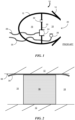
- FIG. 1 is a cross-sectional illustration of an example of a conventional feedback-based acoustic noise reduction (ANR) earbud 10.
- the ANR earbud 10 includes an earbud body 12 which may be formed from plastic or metal and includes a nominally conical section 14 shaped for insertion into the outer portion of the ear canal of a user. The remainder of the body 12 encloses a first acoustic chamber 16 and substantially encloses a second acoustic chamber 18. When worn, the second acoustic chamber 18 extends through the opening 20 in the conical section 14 and into the ear canal of the user.
- a wall 22 separates the internal volume of the earbud body 12 into the two acoustic chambers 16 and 18.
- a speaker 24 is disposed in the wall 22 (or defines part of the wall 22) and an acoustic noise reduction (ANR) microphone 26 is provided in the second acoustic chamber 18.
- ANR acoustic noise reduction
- two pairs of wires 28 and 30 extend through the earbud body 12: one pair 28 coupling the speaker 24 to an electrical audio signal source (not shown) and the second pair 30 coupling the ANR microphone 26 to ANR circuitry (not shown).
- different numbers of wires may be used.
- digital microphones may have electrical connections using three or more wires.
- the wall 22 includes an acoustic port 32 that acoustically connects the first and second acoustic chambers 16 and 18.
- care must be taken to route the wires 28 and 30 though the earbud body 12 and through one or both acoustic chambers 16 and 18 to avoid damaging acoustic components.
- the wires 16 and 18 must maintain reliable electrical connections with the speaker 24 and the ANR microphone 26, and avoid interfering with the acoustic port 32.
- manufacture is generally labor intensive and take considerable time.
- U.S. Patent No. 9,247,335 describes some of the difficulties in routing wires in conventional headphones, and proposes a solution so some of those difficulties; the problems in earbuds are typically similar if not greater.
- Earbud designs might also include other electrical devices, such as optical sources and sensors for heart rate monitoring, and/or accelerometers for fitness tracking functions. These electrical devices can also be present on the circuit board.
- FIG. 2 is a cross-sectional depiction of a portion of an earbud that includes a flexible circuit board assembly 34 (only a portion shown) according to principles described herein.
- a cylindrically-shaped speaker 36 acts as the wall 22 in FIG. 1 that separates the two acoustic chambers 16 and 18.
- the circuit board assembly 34 has a gradual curved shape along a portion of its length to conform to the space between the cylindrical speaker 36 and an adjacent portion of the inner wall 38 of the earbud body 12.
- a channel embedded within the circuit board assembly 34 includes an aperture at each end. One of the apertures is disposed within the first acoustic chamber 16 and the other aperture is disposed within the second acoustic chamber 18. The channel and apertures together define an acoustic channel that acoustically couples the two chambers 16 and 18 to each other.
- FIG. 3A is a top-down view of an example of a flexible electrical circuit board 40 having an embedded acoustic channel.
- the circuit board 40 is unpopulated, that is, no electrical or acoustical components are mounted.
- the dashed rectangular box indicates a portion 42 of the circuit board 40 that includes the embedded acoustic channel that extends between the acoustic chambers.
- the circuit board 40 includes electrically conductive traces 43 (e.g., copper traces) on at least one surface that are used to electrically couple components mounted to the surface at mounting pads or solder pads 44.
- FIG. 3B is a perspective view of the flexible electrical circuit board 40 of FIG. 3A .
- Wires 46 extend from the end of a wiring harness 48 and are coupled to solder pads 44, for example, via solder.
- Components mounted to the circuit board 40 include a feedback microphone 50, an electrical component 52 (e.g., capacitor), a feed-forward microphone 54 and an acoustic driver 56 (e.g., earbud speaker).
- a feedback microphone 50 e.g., an electrical component 52 (e.g., capacitor), a feed-forward microphone 54 and an acoustic driver 56 (e.g., earbud speaker).
- an electrical component 52 e.g., capacitor
- a feed-forward microphone 54 e.g., earbud speaker
- the circuit board 40 can be twisted near one end so that the feedback microphone is located in the first acoustic chamber 16, the electrical component 52 and feed-forward microphone are located in the second acoustic chamber 18, and the acoustic driver 56 is positioned (in a similar way to speaker 36) to separate the two acoustic chambers 16 and 18 with the portion 42 located between the inside wall 38 of the earbud body 12 and the acoustic driver 56.
- the acoustic channel has accurately-controlled dimensions to enable a predetermined acoustic tuning between the two acoustic chambers 16 and 18.
- the flexible nature of the electrical circuit board 40 enables the assembly time for an earbud to be reduced with an associated cost reduction, while a more consistent acoustic performance is achieved for earbuds fabricated to the same design because the fabricated channel maintains its dimensions when the circuit board is assembled to the earbud.
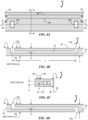
- FIGS. 4A, 4B and 4C are simplified illustrations of a top view, cross-sectional side view and cross-sectional end view, respectively, of an example of an electrical circuit board 60 having an acoustic channel.
- the electrical circuit board 60 is formed of a flexible or rigid dielectric substrate 62 having an upper surface 64 and a lower surface 66 separated by a thickness T.
- the dielectric substrate 62 is a monolithic structure formed of a material having desired dielectric properties.
- the material may be a polyimide, polyester, acrylic or epoxy.
- Electrically conductive traces 68 are formed on the upper surface 64.
- the traces 68 terminate at conductive pads 69 which may be used to electrically connect (e.g., via solder) to an electro-acoustic element or other device.
- conductive pads 69 may be used to electrically connect (e.g., via solder) to an electro-acoustic element or other device.
- additional traces may be provided along the upper surface 64 and that the traces can have more complicated geometries.
- one or more traces may be formed on the lower surface 66, or on both the upper and lower surfaces 64 and 66.
- traces may be formed inside (i.e., embedded within) the dielectric substrate below the upper surface 64 and above the lower surface 66.
- the dielectric substrate includes two or more distinct layers as described in more detail below.
- the layers may include one or more layers of dielectric material, one or more layers of conductive material (e.g., copper layers) and/or one or more layers of adhesive used to securely bond adjacent layers to each other.
- the electrical circuit board 60 includes an acoustic channel embedded in the dielectric substrate 62.
- the acoustic channel includes a channel 70 disposed a distance D below the upper surface 64.
- the channel 70 extends along a length L between a first aperture 72A and a second aperture 72B which form the remainder of the acoustic channel.
- Each of the apertures extends down from the upper surface 64 to meet the respective end of the channel 70.
- FIG. 4D shows an alternative example in which one of the apertures 72C replaces the aperture 72B. In this alternative example, the aperture 72C open to the bottom surface 66 of the dielectric substrate.
- the channel 70 has a width W and a height H which, together with the length L and dimensions of the two apertures 72 define the acoustic impedance of the acoustic channel.
- the dimensions of the acoustic channel can be selected to achieve a desired tuning of the acoustic chambers in an earbud.
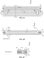
- FIGS. 5A, 5B and 5C are illustrations of a top view, cross-sectional side view and cross-sectional end view, respectively, of another example of an electrical circuit board 80 having an acoustic channel.
- the electrical circuit board 80 is formed of a dielectric substrate having two layers 82 and 84.
- the channel 70 is formed by first forming a groove, or open channel, along a surface of the lower layer 84 that is opposite to the bottom surface 66.
- a laser skiving process can be used to remove a portion of the thickness of the lower layer 64; however, the depth and topography of the resulting groove may be dependent on the homogeneity of the dielectric material.
- the two layers 82 and 84 are then bonded together, for example, using an adhesive.
- the top side of the channel 70 is defined by the inner surface of the upper layer 82 and the remaining three sides of the channel 70 are defined by the shape of the groove.
- the upper layer 82 may be a dielectric layer, an insulating layer or a metallic layer.
- a single layer or "block" of dielectric material having an open channel along a surface i.e., a groove
- a surface of a separate structure such that surface of the separate structure forms the top of the channel.
- the earbud body 12 may provide the top layer of the channel.
- FIGS. 6A, 6B and 6C are illustrations of a top view, cross-sectional side view and cross-sectional end view, respectively, of another example of an electrical circuit board 90 having an acoustic channel.
- the electrical circuit board 90 is formed of a dielectric substrate having three layers: an upper layer 92, an intermediate layer 94 and a lower layer 96 which may be made of similar or different materials.
- an adhesive layer can be used between the upper and intermediate layers 92 and 94, and between the intermediate and lower layers 94 and 96.
- electrically conductive traces 68 may be provided on the lower surface 66 and/or on either or both surfaces of the intermediate layer 94.
- the channel 70 may be formed by using a laser skiving process to remove material from the intermediate layer 94 prior to securing all the layers to each other to form a single structure.
- Laser skiving can be used to remove all the dielectric material in the intermediate layer 94 thereby allowing the thickness of the intermediate layer to accurately define the height of the channel 70.
- the lower layer 96 may be a metallic layer and may be bonded to the intermediate layer 94 before initiating the skiving process. This stops the skiving process at the boundary of the two layers 94 and 96 so that no material from the lower layer 94 is removed.
- additional layers may be present below a metallic lower layer 96.
- the intermediate layer 94 may be a bonding sheet disposed between the upper and lower layers 92 and 96.
- the bonding sheet is provided with a pre-cut portion (e.g., a rectangular opening) that forms an air gap in the multi-layer structure that defines the channel 70.
- the height of the channel 70 is defined by the thickness of the intermediate layer 94.
- a specific thickness of the intermediate layer may be chosen to achieve a desired channel height.
- the layer thicknesses for a flexible circuit board may be less than 10 ⁇ m to more than 30 ⁇ m.
- masking may be used in the laser skiving process to accurately define the width of the material removed from the intermediate layer 94 and thereby limit the width of the channel 70.
- the cross-sectional area of the channel 70 is determined by the channel width and the thickness of the intermediate layer 94.
- the cross-sectional shape of the channel 70 formed in this process is generally rectangular and, if the width is chosen and properly controlled to match the thickness of the intermediate layer 94, the shape of the cross-sectional area is a square which is a preferred rectangular shape for reducing acoustic loss.
- the aspect ratio of the cross-sectional area is less than 10:1 to avoid significant loss.
- an acoustic channel embedded within an electrical circuit board can have a cross-sectional area with dimensions on the order of 0.1 mm2 and may have a length of a few millimeters or greater.
- FIGS. 7A, 7B and 7C are illustrations of a top view, cross-sectional side view and cross-sectional end view, respectively, of another example of an electrical circuit board 100 having an acoustic channel.
- the electrical circuit board 100 is formed of a dielectric substrate having five layers 102, 104, 106, 108 and 110.
- the three intermediate layers 104, 106 and 108 can be processed (e.g., laser skiving) to yield a desired channel height through addition of their individual layer thicknesses.
- the height of the channel 70 may be controlled to the level of the thinnest available layer for the intermediate layers 104, 106 and 108.
- FIG. 7D shows an alternative example in which two of the intermediate layers 104 and 108 each provide a same channel width contribution to a channel 114 whereas intermediate layer 106 provides a greater channel width contribution. Consequently, by forming the channel 114 in multiple intermediate layers, the cross-sectional shape of the channel 114 is not limited to a rectangular shape. The use of even more intermediate layers allows more complicated cross-sectional shapes (e.g., generally elliptical or circular) to be realized; however, the total number of layers can be limited by the thicknesses of the individual layers, acceptable reduction in flexibility, total cross-sectional dimensions and fabrication time and costs.
- the cross-sectional area of the channel is constant along its length; however, an acoustic channel can be formed with a cross-sectional area that varies along the length of the channel.
- the variation in cross-sectional area with length may be used to control acoustic performance at different acoustic frequencies.
- a variation in cross-sectional area can be achieved, for example, by a changing width in one or more intermediate layers along the channel length and/or a changing channel height along the channel length.
- the height of the channel 70 shown in FIGS. 7B and 7C varies along the channel length if the length of the openings in at least two intermediate layers is different.
- the channel structure can vary from the single linear channel configuration described above.
- the channel may be curved.
- two or more channels may be formed in the circuit board.
- Multiple channels may be arranged in parallel and/or may have different cross-sectional dimensions and/or lengths.
Landscapes
- Engineering & Computer Science (AREA)
- Physics & Mathematics (AREA)
- Acoustics & Sound (AREA)
- Signal Processing (AREA)
- Microelectronics & Electronic Packaging (AREA)
- Health & Medical Sciences (AREA)
- Otolaryngology (AREA)
- Structure Of Printed Boards (AREA)
- Electrostatic, Electromagnetic, Magneto- Strictive, And Variable-Resistance Transducers (AREA)
Claims (9)
- Kopfhörer, umfassend:einen Ohrstöpselkörper, der ein Innenvolumen aufweist, das eine erste akustische Kammer und eine zweite akustische Kammer umfasst;ein akustisches Element, das im Innenvolumen zwischen der ersten akustischen Kammer und der zweiten akustischen Kammer angeordnet ist; undein dielektrisches Substrat, das im Innenvolumen angeordnet ist und eine Länge aufweist, die sich von einem ersten Ende in der ersten akustischen Kammer zu einem zweiten Ende in der zweiten akustischen Kammer erstreckt,wobei das dielektrische Substrat eine obere Fläche, eine untere Fläche und einen Kanal umfasst, der zwischen der oberen und der unteren Fläche angeordnet ist,wobei das dielektrische Substrat eine erste Öffnung und eine zweite Öffnung aufweist, die sich jeweils von einer der oberen und der unteren Fläche in eine Dicke des Substrats erstrecken,wobei sich der Kanal von einem ersten Kanalende an der ersten Öffnung zu einem zweiten Kanalende an der zweiten Öffnung erstreckt,wobei die erste und die zweite Öffnung in die erste bzw. die zweite akustische Kammer münden,wobei der Kanal und die erste und die zweite Öffnung einen akustischen Kanal zwischen der ersten und der zweiten akustischen Kammer definieren, der die erste und die zweite akustische Kammer akustisch miteinander koppelt,wobei das dielektrische Substrat ein flexibles dielektrisches Substrat ist.
- Kopfhörer nach Anspruch 1, wobei das dielektrische Substrat eine obere Schicht, eine untere Schicht und eine Zwischenschicht umfasst, die zwischen der oberen und der unteren Schicht angeordnet ist, und wobei der Kanal in der Zwischenschicht gebildet ist.
- Kopfhörer nach Anspruch 1, der weiter eine erste Klebeschicht, die zwischen der oberen Schicht und der Zwischenschicht angeordnet ist, und eine zweite Klebeschicht umfasst, die zwischen der Zwischenschicht und der unteren Schicht angeordnet ist.
- Kopfhörer nach Anspruch 1, wobei das dielektrische Substrat eine erste Schicht umfasst, die an eine zweite Schicht angrenzt, und wobei der Kanal entlang einer Fläche der ersten Schicht angeordnet ist, die an eine Fläche der zweiten Schicht angrenzt.
- Kopfhörer nach Anspruch 4, wobei eine der ersten und der zweiten Schicht eines von einer metallischen Schicht, einer Haftfolie, einer Isolierschicht und einer Versteifungsschicht ist.
- Kopfhörer nach Anspruch 4, der weiter eine Klebeschicht umfasst, die zwischen der ersten und der zweiten Schicht angeordnet ist.
- Kopfhörer nach Anspruch 1, wobei der Kanal einen quadratischen Querschnitt aufweist.
- Kopfhörer nach Anspruch 2, wobei mindestens eine der oberen Schicht, der unteren Schicht und der Zwischenschicht mindestens eines von einer metallischen Schicht, einer Haftfolie, einer Versteifungsschicht und einer Klebeschicht ist.
- Kopfhörer nach Anspruch 2, wobei das dielektrische Substrat eine Vielzahl von Zwischenschichten umfasst, und wobei der Kanal in mindestens zwei der Zwischenschichten gebildet ist.
Applications Claiming Priority (2)
| Application Number | Priority Date | Filing Date | Title |
|---|---|---|---|
| US15/040,465 US9674597B1 (en) | 2016-02-10 | 2016-02-10 | Electrical circuit board with embedded acoustic channel |
| PCT/US2017/014886 WO2017139095A1 (en) | 2016-02-10 | 2017-01-25 | Electrical circuit board with embedded acoustic channel |
Publications (2)
| Publication Number | Publication Date |
|---|---|
| EP3414979A1 EP3414979A1 (de) | 2018-12-19 |
| EP3414979B1 true EP3414979B1 (de) | 2024-07-24 |
Family
ID=57985082
Family Applications (1)
| Application Number | Title | Priority Date | Filing Date |
|---|---|---|---|
| EP17703892.4A Active EP3414979B1 (de) | 2016-02-10 | 2017-01-25 | Elektrische leiterplatte mit integriertem akustischem kanal |
Country Status (4)
| Country | Link |
|---|---|
| US (1) | US9674597B1 (de) |
| EP (1) | EP3414979B1 (de) |
| CN (1) | CN108605410B (de) |
| WO (1) | WO2017139095A1 (de) |
Families Citing this family (4)
| Publication number | Priority date | Publication date | Assignee | Title |
|---|---|---|---|---|
| WO2020038478A1 (zh) * | 2018-08-24 | 2020-02-27 | 深圳市韶音科技有限公司 | 一种眼镜 |
| EP3672279B1 (de) * | 2018-12-19 | 2023-06-07 | Sonova AG | Hörgerät mit aktiver rückkopplungssteuerung |
| CN117241182A (zh) * | 2019-01-05 | 2023-12-15 | 深圳市韶音科技有限公司 | 骨传导扬声装置 |
| DK181160B1 (en) * | 2020-11-30 | 2023-03-09 | Gn Hearing As | Hearing device earpiece having intermediate module |
Citations (3)
| Publication number | Priority date | Publication date | Assignee | Title |
|---|---|---|---|---|
| US20100080405A1 (en) * | 2008-09-26 | 2010-04-01 | Aac Acoustic Technologies (Shenzhen) Co., Ltd | Silicon condenser microphone package |
| US20140363040A1 (en) * | 2013-06-06 | 2014-12-11 | Ryan C. Silvestri | Earphones |
| WO2015022817A1 (ja) * | 2013-08-12 | 2015-02-19 | ソニー株式会社 | ヘッドホン及び音響特性調整方法 |
Family Cites Families (8)
| Publication number | Priority date | Publication date | Assignee | Title |
|---|---|---|---|---|
| US5434362A (en) * | 1994-09-06 | 1995-07-18 | Motorola, Inc. | Flexible circuit board assembly and method |
| US6668064B1 (en) * | 1999-07-06 | 2003-12-23 | Chung Yu Lin | Earphone without impulse noise and surrounding blockade |
| US7480435B2 (en) * | 2005-12-30 | 2009-01-20 | Intel Corporation | Embedded waveguide printed circuit board structure |
| US9137895B2 (en) * | 2008-12-24 | 2015-09-15 | Stmicroelectronics S.R.L. | Micro-electro-mechanical systems (MEMS) and corresponding manufacturing process |
| US9544678B2 (en) * | 2011-01-12 | 2017-01-10 | Blackberry Limited | Printed circuit board with an acoustic channel for a microphone |
| US9197961B2 (en) | 2012-09-14 | 2015-11-24 | Htc Corporation | Portable electronic device with internal speaker |
| US9247335B2 (en) | 2013-03-14 | 2016-01-26 | Bose Corporation | Sealing wiring holes in electronic devices |
| US9532125B2 (en) * | 2014-06-06 | 2016-12-27 | Cirrus Logic, Inc. | Noise cancellation microphones with shared back volume |
-
2016
- 2016-02-10 US US15/040,465 patent/US9674597B1/en active Active
-
2017
- 2017-01-25 CN CN201780010652.5A patent/CN108605410B/zh active Active
- 2017-01-25 EP EP17703892.4A patent/EP3414979B1/de active Active
- 2017-01-25 WO PCT/US2017/014886 patent/WO2017139095A1/en not_active Ceased
Patent Citations (4)
| Publication number | Priority date | Publication date | Assignee | Title |
|---|---|---|---|---|
| US20100080405A1 (en) * | 2008-09-26 | 2010-04-01 | Aac Acoustic Technologies (Shenzhen) Co., Ltd | Silicon condenser microphone package |
| US20140363040A1 (en) * | 2013-06-06 | 2014-12-11 | Ryan C. Silvestri | Earphones |
| WO2015022817A1 (ja) * | 2013-08-12 | 2015-02-19 | ソニー株式会社 | ヘッドホン及び音響特性調整方法 |
| EP3035700A1 (de) * | 2013-08-12 | 2016-06-22 | Sony Corporation | Kopfhörer und verfahren zur anpassung akustischer eigenschaften |
Also Published As
| Publication number | Publication date |
|---|---|
| CN108605410A (zh) | 2018-09-28 |
| US9674597B1 (en) | 2017-06-06 |
| EP3414979A1 (de) | 2018-12-19 |
| WO2017139095A1 (en) | 2017-08-17 |
| CN108605410B (zh) | 2021-09-10 |
Similar Documents
| Publication | Publication Date | Title |
|---|---|---|
| US11968487B2 (en) | Adapters for microphones and combinations thereof | |
| CN103416075B (zh) | 音频设备 | |
| US9738515B2 (en) | Transducer with enlarged back volume | |
| EP3414979B1 (de) | Elektrische leiterplatte mit integriertem akustischem kanal | |
| JP4913907B2 (ja) | 可変指向性マイクロホン組立体及びその製造方法 | |
| US20080150104A1 (en) | Leadframe with different topologies for mems package | |
| US20070040231A1 (en) | Partially etched leadframe packages having different top and bottom topologies | |
| KR101931168B1 (ko) | 지향성 마이크로폰 | |
| WO2013028399A2 (en) | Acoustic apparatus and method of manufacturing | |
| US10779077B2 (en) | Microphone cavity | |
| KR20210036846A (ko) | 가청 파장 범위 및/또는 초음파 범위의 음파를 생성 및/또는 검출하기 위한 사운드 변환기 유닛 | |
| EP3101914B1 (de) | Mikrofonaufbau mit eingebetteter akustiköffnung | |
| US10252906B2 (en) | Package for MEMS device and process | |
| EP3837856B1 (de) | Zweischichtiger mikrofonschutz | |
| US20250254453A1 (en) | Apparatus and method for mems microphone performance via back volume | |
| US6459800B1 (en) | Modular hearing device receiver suspension | |
| US7165647B2 (en) | Mechanical acoustic filter by erosion etching | |
| CN218772430U (zh) | Mems麦克风和电子设备 | |
| EP2786592B1 (de) | Elektroakustischer wandler zur montage auf einem substrat | |
| KR102079978B1 (ko) | 지향성 멤스 마이크로폰 하우징 | |
| JP2006311106A (ja) | 音響センサ | |
| JP2006311105A (ja) | 音響センサ |
Legal Events
| Date | Code | Title | Description |
|---|---|---|---|
| STAA | Information on the status of an ep patent application or granted ep patent |
Free format text: STATUS: UNKNOWN |
|
| STAA | Information on the status of an ep patent application or granted ep patent |
Free format text: STATUS: THE INTERNATIONAL PUBLICATION HAS BEEN MADE |
|
| PUAI | Public reference made under article 153(3) epc to a published international application that has entered the european phase |
Free format text: ORIGINAL CODE: 0009012 |
|
| STAA | Information on the status of an ep patent application or granted ep patent |
Free format text: STATUS: REQUEST FOR EXAMINATION WAS MADE |
|
| 17P | Request for examination filed |
Effective date: 20180821 |
|
| AK | Designated contracting states |
Kind code of ref document: A1 Designated state(s): AL AT BE BG CH CY CZ DE DK EE ES FI FR GB GR HR HU IE IS IT LI LT LU LV MC MK MT NL NO PL PT RO RS SE SI SK SM TR |
|
| AX | Request for extension of the european patent |
Extension state: BA ME |
|
| DAV | Request for validation of the european patent (deleted) | ||
| DAX | Request for extension of the european patent (deleted) | ||
| STAA | Information on the status of an ep patent application or granted ep patent |
Free format text: STATUS: EXAMINATION IS IN PROGRESS |
|
| PUAG | Search results despatched under rule 164(2) epc together with communication from examining division |
Free format text: ORIGINAL CODE: 0009017 |
|
| 17Q | First examination report despatched |
Effective date: 20190531 |
|
| B565 | Issuance of search results under rule 164(2) epc |
Effective date: 20190531 |
|
| RIC1 | Information provided on ipc code assigned before grant |
Ipc: H04R 1/10 20060101ALI20190527BHEP Ipc: H05K 1/02 20060101AFI20190527BHEP Ipc: H04R 5/033 20060101ALI20190527BHEP Ipc: H04R 1/28 20060101ALN20190527BHEP |
|
| GRAP | Despatch of communication of intention to grant a patent |
Free format text: ORIGINAL CODE: EPIDOSNIGR1 |
|
| STAA | Information on the status of an ep patent application or granted ep patent |
Free format text: STATUS: GRANT OF PATENT IS INTENDED |
|
| RIC1 | Information provided on ipc code assigned before grant |
Ipc: H04R 1/28 20060101ALN20240402BHEP Ipc: H04R 5/033 20060101ALI20240402BHEP Ipc: H04R 1/10 20060101ALI20240402BHEP Ipc: H05K 1/02 20060101AFI20240402BHEP |
|
| INTG | Intention to grant announced |
Effective date: 20240418 |
|
| GRAS | Grant fee paid |
Free format text: ORIGINAL CODE: EPIDOSNIGR3 |
|
| GRAA | (expected) grant |
Free format text: ORIGINAL CODE: 0009210 |
|
| STAA | Information on the status of an ep patent application or granted ep patent |
Free format text: STATUS: THE PATENT HAS BEEN GRANTED |
|
| AK | Designated contracting states |
Kind code of ref document: B1 Designated state(s): AL AT BE BG CH CY CZ DE DK EE ES FI FR GB GR HR HU IE IS IT LI LT LU LV MC MK MT NL NO PL PT RO RS SE SI SK SM TR |
|
| REG | Reference to a national code |
Ref country code: GB Ref legal event code: FG4D |
|
| REG | Reference to a national code |
Ref country code: CH Ref legal event code: EP |
|
| REG | Reference to a national code |
Ref country code: IE Ref legal event code: FG4D Ref country code: DE Ref legal event code: R096 Ref document number: 602017083488 Country of ref document: DE |
|
| REG | Reference to a national code |
Ref country code: LT Ref legal event code: MG9D |
|
| REG | Reference to a national code |
Ref country code: NL Ref legal event code: MP Effective date: 20240724 |
|
| PG25 | Lapsed in a contracting state [announced via postgrant information from national office to epo] |
Ref country code: PT Free format text: LAPSE BECAUSE OF FAILURE TO SUBMIT A TRANSLATION OF THE DESCRIPTION OR TO PAY THE FEE WITHIN THE PRESCRIBED TIME-LIMIT Effective date: 20241125 |
|
| REG | Reference to a national code |
Ref country code: AT Ref legal event code: MK05 Ref document number: 1707494 Country of ref document: AT Kind code of ref document: T Effective date: 20240724 |
|
| PG25 | Lapsed in a contracting state [announced via postgrant information from national office to epo] |
Ref country code: NL Free format text: LAPSE BECAUSE OF FAILURE TO SUBMIT A TRANSLATION OF THE DESCRIPTION OR TO PAY THE FEE WITHIN THE PRESCRIBED TIME-LIMIT Effective date: 20240724 |
|
| PG25 | Lapsed in a contracting state [announced via postgrant information from national office to epo] |
Ref country code: PT Free format text: LAPSE BECAUSE OF FAILURE TO SUBMIT A TRANSLATION OF THE DESCRIPTION OR TO PAY THE FEE WITHIN THE PRESCRIBED TIME-LIMIT Effective date: 20241125 Ref country code: NL Free format text: LAPSE BECAUSE OF FAILURE TO SUBMIT A TRANSLATION OF THE DESCRIPTION OR TO PAY THE FEE WITHIN THE PRESCRIBED TIME-LIMIT Effective date: 20240724 |
|
| PG25 | Lapsed in a contracting state [announced via postgrant information from national office to epo] |
Ref country code: NO Free format text: LAPSE BECAUSE OF FAILURE TO SUBMIT A TRANSLATION OF THE DESCRIPTION OR TO PAY THE FEE WITHIN THE PRESCRIBED TIME-LIMIT Effective date: 20241024 |
|
| PG25 | Lapsed in a contracting state [announced via postgrant information from national office to epo] |
Ref country code: FI Free format text: LAPSE BECAUSE OF FAILURE TO SUBMIT A TRANSLATION OF THE DESCRIPTION OR TO PAY THE FEE WITHIN THE PRESCRIBED TIME-LIMIT Effective date: 20240724 Ref country code: GR Free format text: LAPSE BECAUSE OF FAILURE TO SUBMIT A TRANSLATION OF THE DESCRIPTION OR TO PAY THE FEE WITHIN THE PRESCRIBED TIME-LIMIT Effective date: 20241025 Ref country code: PL Free format text: LAPSE BECAUSE OF FAILURE TO SUBMIT A TRANSLATION OF THE DESCRIPTION OR TO PAY THE FEE WITHIN THE PRESCRIBED TIME-LIMIT Effective date: 20240724 |
|
| PG25 | Lapsed in a contracting state [announced via postgrant information from national office to epo] |
Ref country code: BG Free format text: LAPSE BECAUSE OF FAILURE TO SUBMIT A TRANSLATION OF THE DESCRIPTION OR TO PAY THE FEE WITHIN THE PRESCRIBED TIME-LIMIT Effective date: 20240724 |
|
| PG25 | Lapsed in a contracting state [announced via postgrant information from national office to epo] |
Ref country code: LV Free format text: LAPSE BECAUSE OF FAILURE TO SUBMIT A TRANSLATION OF THE DESCRIPTION OR TO PAY THE FEE WITHIN THE PRESCRIBED TIME-LIMIT Effective date: 20240724 |
|
| PG25 | Lapsed in a contracting state [announced via postgrant information from national office to epo] |
Ref country code: IS Free format text: LAPSE BECAUSE OF FAILURE TO SUBMIT A TRANSLATION OF THE DESCRIPTION OR TO PAY THE FEE WITHIN THE PRESCRIBED TIME-LIMIT Effective date: 20241124 Ref country code: AT Free format text: LAPSE BECAUSE OF FAILURE TO SUBMIT A TRANSLATION OF THE DESCRIPTION OR TO PAY THE FEE WITHIN THE PRESCRIBED TIME-LIMIT Effective date: 20240724 |
|
| PG25 | Lapsed in a contracting state [announced via postgrant information from national office to epo] |
Ref country code: HR Free format text: LAPSE BECAUSE OF FAILURE TO SUBMIT A TRANSLATION OF THE DESCRIPTION OR TO PAY THE FEE WITHIN THE PRESCRIBED TIME-LIMIT Effective date: 20240724 |
|
| PG25 | Lapsed in a contracting state [announced via postgrant information from national office to epo] |
Ref country code: ES Free format text: LAPSE BECAUSE OF FAILURE TO SUBMIT A TRANSLATION OF THE DESCRIPTION OR TO PAY THE FEE WITHIN THE PRESCRIBED TIME-LIMIT Effective date: 20240724 Ref country code: RS Free format text: LAPSE BECAUSE OF FAILURE TO SUBMIT A TRANSLATION OF THE DESCRIPTION OR TO PAY THE FEE WITHIN THE PRESCRIBED TIME-LIMIT Effective date: 20241024 |
|
| PG25 | Lapsed in a contracting state [announced via postgrant information from national office to epo] |
Ref country code: RS Free format text: LAPSE BECAUSE OF FAILURE TO SUBMIT A TRANSLATION OF THE DESCRIPTION OR TO PAY THE FEE WITHIN THE PRESCRIBED TIME-LIMIT Effective date: 20241024 Ref country code: PL Free format text: LAPSE BECAUSE OF FAILURE TO SUBMIT A TRANSLATION OF THE DESCRIPTION OR TO PAY THE FEE WITHIN THE PRESCRIBED TIME-LIMIT Effective date: 20240724 Ref country code: NO Free format text: LAPSE BECAUSE OF FAILURE TO SUBMIT A TRANSLATION OF THE DESCRIPTION OR TO PAY THE FEE WITHIN THE PRESCRIBED TIME-LIMIT Effective date: 20241024 Ref country code: LV Free format text: LAPSE BECAUSE OF FAILURE TO SUBMIT A TRANSLATION OF THE DESCRIPTION OR TO PAY THE FEE WITHIN THE PRESCRIBED TIME-LIMIT Effective date: 20240724 Ref country code: IS Free format text: LAPSE BECAUSE OF FAILURE TO SUBMIT A TRANSLATION OF THE DESCRIPTION OR TO PAY THE FEE WITHIN THE PRESCRIBED TIME-LIMIT Effective date: 20241124 Ref country code: HR Free format text: LAPSE BECAUSE OF FAILURE TO SUBMIT A TRANSLATION OF THE DESCRIPTION OR TO PAY THE FEE WITHIN THE PRESCRIBED TIME-LIMIT Effective date: 20240724 Ref country code: GR Free format text: LAPSE BECAUSE OF FAILURE TO SUBMIT A TRANSLATION OF THE DESCRIPTION OR TO PAY THE FEE WITHIN THE PRESCRIBED TIME-LIMIT Effective date: 20241025 Ref country code: FI Free format text: LAPSE BECAUSE OF FAILURE TO SUBMIT A TRANSLATION OF THE DESCRIPTION OR TO PAY THE FEE WITHIN THE PRESCRIBED TIME-LIMIT Effective date: 20240724 Ref country code: ES Free format text: LAPSE BECAUSE OF FAILURE TO SUBMIT A TRANSLATION OF THE DESCRIPTION OR TO PAY THE FEE WITHIN THE PRESCRIBED TIME-LIMIT Effective date: 20240724 Ref country code: BG Free format text: LAPSE BECAUSE OF FAILURE TO SUBMIT A TRANSLATION OF THE DESCRIPTION OR TO PAY THE FEE WITHIN THE PRESCRIBED TIME-LIMIT Effective date: 20240724 Ref country code: AT Free format text: LAPSE BECAUSE OF FAILURE TO SUBMIT A TRANSLATION OF THE DESCRIPTION OR TO PAY THE FEE WITHIN THE PRESCRIBED TIME-LIMIT Effective date: 20240724 |
|
| PG25 | Lapsed in a contracting state [announced via postgrant information from national office to epo] |
Ref country code: DK Free format text: LAPSE BECAUSE OF FAILURE TO SUBMIT A TRANSLATION OF THE DESCRIPTION OR TO PAY THE FEE WITHIN THE PRESCRIBED TIME-LIMIT Effective date: 20240724 Ref country code: SM Free format text: LAPSE BECAUSE OF FAILURE TO SUBMIT A TRANSLATION OF THE DESCRIPTION OR TO PAY THE FEE WITHIN THE PRESCRIBED TIME-LIMIT Effective date: 20240724 Ref country code: RO Free format text: LAPSE BECAUSE OF FAILURE TO SUBMIT A TRANSLATION OF THE DESCRIPTION OR TO PAY THE FEE WITHIN THE PRESCRIBED TIME-LIMIT Effective date: 20240724 |
|
| PG25 | Lapsed in a contracting state [announced via postgrant information from national office to epo] |
Ref country code: EE Free format text: LAPSE BECAUSE OF FAILURE TO SUBMIT A TRANSLATION OF THE DESCRIPTION OR TO PAY THE FEE WITHIN THE PRESCRIBED TIME-LIMIT Effective date: 20240724 |
|
| PG25 | Lapsed in a contracting state [announced via postgrant information from national office to epo] |
Ref country code: CZ Free format text: LAPSE BECAUSE OF FAILURE TO SUBMIT A TRANSLATION OF THE DESCRIPTION OR TO PAY THE FEE WITHIN THE PRESCRIBED TIME-LIMIT Effective date: 20240724 |
|
| REG | Reference to a national code |
Ref country code: DE Ref legal event code: R097 Ref document number: 602017083488 Country of ref document: DE |
|
| PG25 | Lapsed in a contracting state [announced via postgrant information from national office to epo] |
Ref country code: IT Free format text: LAPSE BECAUSE OF FAILURE TO SUBMIT A TRANSLATION OF THE DESCRIPTION OR TO PAY THE FEE WITHIN THE PRESCRIBED TIME-LIMIT Effective date: 20240724 Ref country code: SK Free format text: LAPSE BECAUSE OF FAILURE TO SUBMIT A TRANSLATION OF THE DESCRIPTION OR TO PAY THE FEE WITHIN THE PRESCRIBED TIME-LIMIT Effective date: 20240724 |
|
| PLBE | No opposition filed within time limit |
Free format text: ORIGINAL CODE: 0009261 |
|
| STAA | Information on the status of an ep patent application or granted ep patent |
Free format text: STATUS: NO OPPOSITION FILED WITHIN TIME LIMIT |
|
| 26N | No opposition filed |
Effective date: 20250425 |
|
| REG | Reference to a national code |
Ref country code: CH Ref legal event code: PL |
|
| PG25 | Lapsed in a contracting state [announced via postgrant information from national office to epo] |
Ref country code: SE Free format text: LAPSE BECAUSE OF FAILURE TO SUBMIT A TRANSLATION OF THE DESCRIPTION OR TO PAY THE FEE WITHIN THE PRESCRIBED TIME-LIMIT Effective date: 20240724 |
|
| PG25 | Lapsed in a contracting state [announced via postgrant information from national office to epo] |
Ref country code: MC Free format text: LAPSE BECAUSE OF FAILURE TO SUBMIT A TRANSLATION OF THE DESCRIPTION OR TO PAY THE FEE WITHIN THE PRESCRIBED TIME-LIMIT Effective date: 20240724 Ref country code: LU Free format text: LAPSE BECAUSE OF NON-PAYMENT OF DUE FEES Effective date: 20250125 |
|
| PG25 | Lapsed in a contracting state [announced via postgrant information from national office to epo] |
Ref country code: BE Free format text: LAPSE BECAUSE OF NON-PAYMENT OF DUE FEES Effective date: 20250131 |
|
| PG25 | Lapsed in a contracting state [announced via postgrant information from national office to epo] |
Ref country code: CH Free format text: LAPSE BECAUSE OF NON-PAYMENT OF DUE FEES Effective date: 20250131 |
|
| REG | Reference to a national code |
Ref country code: BE Ref legal event code: MM Effective date: 20250131 |
|
| PGFP | Annual fee paid to national office [announced via postgrant information from national office to epo] |
Ref country code: GB Payment date: 20251220 Year of fee payment: 10 |
|
| PGFP | Annual fee paid to national office [announced via postgrant information from national office to epo] |
Ref country code: FR Payment date: 20251218 Year of fee payment: 10 |
|
| PG25 | Lapsed in a contracting state [announced via postgrant information from national office to epo] |
Ref country code: IE Free format text: LAPSE BECAUSE OF NON-PAYMENT OF DUE FEES Effective date: 20250125 |
|
| PGFP | Annual fee paid to national office [announced via postgrant information from national office to epo] |
Ref country code: DE Payment date: 20251217 Year of fee payment: 10 |