EP3420117B1 - Zusammensetzungen und verfahren mit verwendung davon zur abscheidung von siliciumhaltigem film - Google Patents
Zusammensetzungen und verfahren mit verwendung davon zur abscheidung von siliciumhaltigem film Download PDFInfo
- Publication number
- EP3420117B1 EP3420117B1 EP17757122.1A EP17757122A EP3420117B1 EP 3420117 B1 EP3420117 B1 EP 3420117B1 EP 17757122 A EP17757122 A EP 17757122A EP 3420117 B1 EP3420117 B1 EP 3420117B1
- Authority
- EP
- European Patent Office
- Prior art keywords
- plasma
- branched
- group
- linear
- compound
- Prior art date
- Legal status (The legal status is an assumption and is not a legal conclusion. Google has not performed a legal analysis and makes no representation as to the accuracy of the status listed.)
- Active
Links
Images


Classifications
-
- C—CHEMISTRY; METALLURGY
- C23—COATING METALLIC MATERIAL; COATING MATERIAL WITH METALLIC MATERIAL; CHEMICAL SURFACE TREATMENT; DIFFUSION TREATMENT OF METALLIC MATERIAL; COATING BY VACUUM EVAPORATION, BY SPUTTERING, BY ION IMPLANTATION OR BY CHEMICAL VAPOUR DEPOSITION, IN GENERAL; INHIBITING CORROSION OF METALLIC MATERIAL OR INCRUSTATION IN GENERAL
- C23C—COATING METALLIC MATERIAL; COATING MATERIAL WITH METALLIC MATERIAL; SURFACE TREATMENT OF METALLIC MATERIAL BY DIFFUSION INTO THE SURFACE, BY CHEMICAL CONVERSION OR SUBSTITUTION; COATING BY VACUUM EVAPORATION, BY SPUTTERING, BY ION IMPLANTATION OR BY CHEMICAL VAPOUR DEPOSITION, IN GENERAL
- C23C16/00—Chemical coating by decomposition of gaseous compounds, without leaving reaction products of surface material in the coating, i.e. chemical vapour deposition [CVD] processes
- C23C16/22—Chemical coating by decomposition of gaseous compounds, without leaving reaction products of surface material in the coating, i.e. chemical vapour deposition [CVD] processes characterised by the deposition of inorganic material, other than metallic material
- C23C16/30—Deposition of compounds, mixtures or solid solutions, e.g. borides, carbides, nitrides
-
- C—CHEMISTRY; METALLURGY
- C23—COATING METALLIC MATERIAL; COATING MATERIAL WITH METALLIC MATERIAL; CHEMICAL SURFACE TREATMENT; DIFFUSION TREATMENT OF METALLIC MATERIAL; COATING BY VACUUM EVAPORATION, BY SPUTTERING, BY ION IMPLANTATION OR BY CHEMICAL VAPOUR DEPOSITION, IN GENERAL; INHIBITING CORROSION OF METALLIC MATERIAL OR INCRUSTATION IN GENERAL
- C23C—COATING METALLIC MATERIAL; COATING MATERIAL WITH METALLIC MATERIAL; SURFACE TREATMENT OF METALLIC MATERIAL BY DIFFUSION INTO THE SURFACE, BY CHEMICAL CONVERSION OR SUBSTITUTION; COATING BY VACUUM EVAPORATION, BY SPUTTERING, BY ION IMPLANTATION OR BY CHEMICAL VAPOUR DEPOSITION, IN GENERAL
- C23C16/00—Chemical coating by decomposition of gaseous compounds, without leaving reaction products of surface material in the coating, i.e. chemical vapour deposition [CVD] processes
- C23C16/04—Coating on selected surface areas, e.g. using masks
- C23C16/045—Coating cavities or hollow spaces, e.g. interior of tubes; Infiltration of porous substrates
-
- C—CHEMISTRY; METALLURGY
- C23—COATING METALLIC MATERIAL; COATING MATERIAL WITH METALLIC MATERIAL; CHEMICAL SURFACE TREATMENT; DIFFUSION TREATMENT OF METALLIC MATERIAL; COATING BY VACUUM EVAPORATION, BY SPUTTERING, BY ION IMPLANTATION OR BY CHEMICAL VAPOUR DEPOSITION, IN GENERAL; INHIBITING CORROSION OF METALLIC MATERIAL OR INCRUSTATION IN GENERAL
- C23C—COATING METALLIC MATERIAL; COATING MATERIAL WITH METALLIC MATERIAL; SURFACE TREATMENT OF METALLIC MATERIAL BY DIFFUSION INTO THE SURFACE, BY CHEMICAL CONVERSION OR SUBSTITUTION; COATING BY VACUUM EVAPORATION, BY SPUTTERING, BY ION IMPLANTATION OR BY CHEMICAL VAPOUR DEPOSITION, IN GENERAL
- C23C16/00—Chemical coating by decomposition of gaseous compounds, without leaving reaction products of surface material in the coating, i.e. chemical vapour deposition [CVD] processes
- C23C16/22—Chemical coating by decomposition of gaseous compounds, without leaving reaction products of surface material in the coating, i.e. chemical vapour deposition [CVD] processes characterised by the deposition of inorganic material, other than metallic material
- C23C16/30—Deposition of compounds, mixtures or solid solutions, e.g. borides, carbides, nitrides
- C23C16/308—Oxynitrides
-
- C—CHEMISTRY; METALLURGY
- C23—COATING METALLIC MATERIAL; COATING MATERIAL WITH METALLIC MATERIAL; CHEMICAL SURFACE TREATMENT; DIFFUSION TREATMENT OF METALLIC MATERIAL; COATING BY VACUUM EVAPORATION, BY SPUTTERING, BY ION IMPLANTATION OR BY CHEMICAL VAPOUR DEPOSITION, IN GENERAL; INHIBITING CORROSION OF METALLIC MATERIAL OR INCRUSTATION IN GENERAL
- C23C—COATING METALLIC MATERIAL; COATING MATERIAL WITH METALLIC MATERIAL; SURFACE TREATMENT OF METALLIC MATERIAL BY DIFFUSION INTO THE SURFACE, BY CHEMICAL CONVERSION OR SUBSTITUTION; COATING BY VACUUM EVAPORATION, BY SPUTTERING, BY ION IMPLANTATION OR BY CHEMICAL VAPOUR DEPOSITION, IN GENERAL
- C23C16/00—Chemical coating by decomposition of gaseous compounds, without leaving reaction products of surface material in the coating, i.e. chemical vapour deposition [CVD] processes
- C23C16/22—Chemical coating by decomposition of gaseous compounds, without leaving reaction products of surface material in the coating, i.e. chemical vapour deposition [CVD] processes characterised by the deposition of inorganic material, other than metallic material
- C23C16/30—Deposition of compounds, mixtures or solid solutions, e.g. borides, carbides, nitrides
- C23C16/32—Carbides
- C23C16/325—Silicon carbide
-
- C—CHEMISTRY; METALLURGY
- C23—COATING METALLIC MATERIAL; COATING MATERIAL WITH METALLIC MATERIAL; CHEMICAL SURFACE TREATMENT; DIFFUSION TREATMENT OF METALLIC MATERIAL; COATING BY VACUUM EVAPORATION, BY SPUTTERING, BY ION IMPLANTATION OR BY CHEMICAL VAPOUR DEPOSITION, IN GENERAL; INHIBITING CORROSION OF METALLIC MATERIAL OR INCRUSTATION IN GENERAL
- C23C—COATING METALLIC MATERIAL; COATING MATERIAL WITH METALLIC MATERIAL; SURFACE TREATMENT OF METALLIC MATERIAL BY DIFFUSION INTO THE SURFACE, BY CHEMICAL CONVERSION OR SUBSTITUTION; COATING BY VACUUM EVAPORATION, BY SPUTTERING, BY ION IMPLANTATION OR BY CHEMICAL VAPOUR DEPOSITION, IN GENERAL
- C23C16/00—Chemical coating by decomposition of gaseous compounds, without leaving reaction products of surface material in the coating, i.e. chemical vapour deposition [CVD] processes
- C23C16/22—Chemical coating by decomposition of gaseous compounds, without leaving reaction products of surface material in the coating, i.e. chemical vapour deposition [CVD] processes characterised by the deposition of inorganic material, other than metallic material
- C23C16/30—Deposition of compounds, mixtures or solid solutions, e.g. borides, carbides, nitrides
- C23C16/34—Nitrides
- C23C16/345—Silicon nitride
-
- C—CHEMISTRY; METALLURGY
- C23—COATING METALLIC MATERIAL; COATING MATERIAL WITH METALLIC MATERIAL; CHEMICAL SURFACE TREATMENT; DIFFUSION TREATMENT OF METALLIC MATERIAL; COATING BY VACUUM EVAPORATION, BY SPUTTERING, BY ION IMPLANTATION OR BY CHEMICAL VAPOUR DEPOSITION, IN GENERAL; INHIBITING CORROSION OF METALLIC MATERIAL OR INCRUSTATION IN GENERAL
- C23C—COATING METALLIC MATERIAL; COATING MATERIAL WITH METALLIC MATERIAL; SURFACE TREATMENT OF METALLIC MATERIAL BY DIFFUSION INTO THE SURFACE, BY CHEMICAL CONVERSION OR SUBSTITUTION; COATING BY VACUUM EVAPORATION, BY SPUTTERING, BY ION IMPLANTATION OR BY CHEMICAL VAPOUR DEPOSITION, IN GENERAL
- C23C16/00—Chemical coating by decomposition of gaseous compounds, without leaving reaction products of surface material in the coating, i.e. chemical vapour deposition [CVD] processes
- C23C16/22—Chemical coating by decomposition of gaseous compounds, without leaving reaction products of surface material in the coating, i.e. chemical vapour deposition [CVD] processes characterised by the deposition of inorganic material, other than metallic material
- C23C16/30—Deposition of compounds, mixtures or solid solutions, e.g. borides, carbides, nitrides
- C23C16/36—Carbonitrides
-
- C—CHEMISTRY; METALLURGY
- C23—COATING METALLIC MATERIAL; COATING MATERIAL WITH METALLIC MATERIAL; CHEMICAL SURFACE TREATMENT; DIFFUSION TREATMENT OF METALLIC MATERIAL; COATING BY VACUUM EVAPORATION, BY SPUTTERING, BY ION IMPLANTATION OR BY CHEMICAL VAPOUR DEPOSITION, IN GENERAL; INHIBITING CORROSION OF METALLIC MATERIAL OR INCRUSTATION IN GENERAL
- C23C—COATING METALLIC MATERIAL; COATING MATERIAL WITH METALLIC MATERIAL; SURFACE TREATMENT OF METALLIC MATERIAL BY DIFFUSION INTO THE SURFACE, BY CHEMICAL CONVERSION OR SUBSTITUTION; COATING BY VACUUM EVAPORATION, BY SPUTTERING, BY ION IMPLANTATION OR BY CHEMICAL VAPOUR DEPOSITION, IN GENERAL
- C23C16/00—Chemical coating by decomposition of gaseous compounds, without leaving reaction products of surface material in the coating, i.e. chemical vapour deposition [CVD] processes
- C23C16/22—Chemical coating by decomposition of gaseous compounds, without leaving reaction products of surface material in the coating, i.e. chemical vapour deposition [CVD] processes characterised by the deposition of inorganic material, other than metallic material
- C23C16/30—Deposition of compounds, mixtures or solid solutions, e.g. borides, carbides, nitrides
- C23C16/40—Oxides
- C23C16/401—Oxides containing silicon
-
- C—CHEMISTRY; METALLURGY
- C23—COATING METALLIC MATERIAL; COATING MATERIAL WITH METALLIC MATERIAL; CHEMICAL SURFACE TREATMENT; DIFFUSION TREATMENT OF METALLIC MATERIAL; COATING BY VACUUM EVAPORATION, BY SPUTTERING, BY ION IMPLANTATION OR BY CHEMICAL VAPOUR DEPOSITION, IN GENERAL; INHIBITING CORROSION OF METALLIC MATERIAL OR INCRUSTATION IN GENERAL
- C23C—COATING METALLIC MATERIAL; COATING MATERIAL WITH METALLIC MATERIAL; SURFACE TREATMENT OF METALLIC MATERIAL BY DIFFUSION INTO THE SURFACE, BY CHEMICAL CONVERSION OR SUBSTITUTION; COATING BY VACUUM EVAPORATION, BY SPUTTERING, BY ION IMPLANTATION OR BY CHEMICAL VAPOUR DEPOSITION, IN GENERAL
- C23C16/00—Chemical coating by decomposition of gaseous compounds, without leaving reaction products of surface material in the coating, i.e. chemical vapour deposition [CVD] processes
- C23C16/44—Chemical coating by decomposition of gaseous compounds, without leaving reaction products of surface material in the coating, i.e. chemical vapour deposition [CVD] processes characterised by the method of coating
- C23C16/455—Chemical coating by decomposition of gaseous compounds, without leaving reaction products of surface material in the coating, i.e. chemical vapour deposition [CVD] processes characterised by the method of coating characterised by the method used for introducing gases into reaction chamber or for modifying gas flows in reaction chamber
- C23C16/45523—Pulsed gas flow or change of composition over time
- C23C16/45525—Atomic layer deposition [ALD]
- C23C16/45553—Atomic layer deposition [ALD] characterized by the use of precursors specially adapted for ALD
-
- C—CHEMISTRY; METALLURGY
- C23—COATING METALLIC MATERIAL; COATING MATERIAL WITH METALLIC MATERIAL; CHEMICAL SURFACE TREATMENT; DIFFUSION TREATMENT OF METALLIC MATERIAL; COATING BY VACUUM EVAPORATION, BY SPUTTERING, BY ION IMPLANTATION OR BY CHEMICAL VAPOUR DEPOSITION, IN GENERAL; INHIBITING CORROSION OF METALLIC MATERIAL OR INCRUSTATION IN GENERAL
- C23C—COATING METALLIC MATERIAL; COATING MATERIAL WITH METALLIC MATERIAL; SURFACE TREATMENT OF METALLIC MATERIAL BY DIFFUSION INTO THE SURFACE, BY CHEMICAL CONVERSION OR SUBSTITUTION; COATING BY VACUUM EVAPORATION, BY SPUTTERING, BY ION IMPLANTATION OR BY CHEMICAL VAPOUR DEPOSITION, IN GENERAL
- C23C16/00—Chemical coating by decomposition of gaseous compounds, without leaving reaction products of surface material in the coating, i.e. chemical vapour deposition [CVD] processes
- C23C16/44—Chemical coating by decomposition of gaseous compounds, without leaving reaction products of surface material in the coating, i.e. chemical vapour deposition [CVD] processes characterised by the method of coating
- C23C16/46—Chemical coating by decomposition of gaseous compounds, without leaving reaction products of surface material in the coating, i.e. chemical vapour deposition [CVD] processes characterised by the method of coating characterised by the method used for heating the substrate
-
- C—CHEMISTRY; METALLURGY
- C23—COATING METALLIC MATERIAL; COATING MATERIAL WITH METALLIC MATERIAL; CHEMICAL SURFACE TREATMENT; DIFFUSION TREATMENT OF METALLIC MATERIAL; COATING BY VACUUM EVAPORATION, BY SPUTTERING, BY ION IMPLANTATION OR BY CHEMICAL VAPOUR DEPOSITION, IN GENERAL; INHIBITING CORROSION OF METALLIC MATERIAL OR INCRUSTATION IN GENERAL
- C23C—COATING METALLIC MATERIAL; COATING MATERIAL WITH METALLIC MATERIAL; SURFACE TREATMENT OF METALLIC MATERIAL BY DIFFUSION INTO THE SURFACE, BY CHEMICAL CONVERSION OR SUBSTITUTION; COATING BY VACUUM EVAPORATION, BY SPUTTERING, BY ION IMPLANTATION OR BY CHEMICAL VAPOUR DEPOSITION, IN GENERAL
- C23C16/00—Chemical coating by decomposition of gaseous compounds, without leaving reaction products of surface material in the coating, i.e. chemical vapour deposition [CVD] processes
- C23C16/44—Chemical coating by decomposition of gaseous compounds, without leaving reaction products of surface material in the coating, i.e. chemical vapour deposition [CVD] processes characterised by the method of coating
- C23C16/50—Chemical coating by decomposition of gaseous compounds, without leaving reaction products of surface material in the coating, i.e. chemical vapour deposition [CVD] processes characterised by the method of coating using electric discharges
- C23C16/505—Chemical coating by decomposition of gaseous compounds, without leaving reaction products of surface material in the coating, i.e. chemical vapour deposition [CVD] processes characterised by the method of coating using electric discharges using radio frequency discharges
-
- C—CHEMISTRY; METALLURGY
- C23—COATING METALLIC MATERIAL; COATING MATERIAL WITH METALLIC MATERIAL; CHEMICAL SURFACE TREATMENT; DIFFUSION TREATMENT OF METALLIC MATERIAL; COATING BY VACUUM EVAPORATION, BY SPUTTERING, BY ION IMPLANTATION OR BY CHEMICAL VAPOUR DEPOSITION, IN GENERAL; INHIBITING CORROSION OF METALLIC MATERIAL OR INCRUSTATION IN GENERAL
- C23C—COATING METALLIC MATERIAL; COATING MATERIAL WITH METALLIC MATERIAL; SURFACE TREATMENT OF METALLIC MATERIAL BY DIFFUSION INTO THE SURFACE, BY CHEMICAL CONVERSION OR SUBSTITUTION; COATING BY VACUUM EVAPORATION, BY SPUTTERING, BY ION IMPLANTATION OR BY CHEMICAL VAPOUR DEPOSITION, IN GENERAL
- C23C16/00—Chemical coating by decomposition of gaseous compounds, without leaving reaction products of surface material in the coating, i.e. chemical vapour deposition [CVD] processes
- C23C16/44—Chemical coating by decomposition of gaseous compounds, without leaving reaction products of surface material in the coating, i.e. chemical vapour deposition [CVD] processes characterised by the method of coating
- C23C16/50—Chemical coating by decomposition of gaseous compounds, without leaving reaction products of surface material in the coating, i.e. chemical vapour deposition [CVD] processes characterised by the method of coating using electric discharges
- C23C16/513—Chemical coating by decomposition of gaseous compounds, without leaving reaction products of surface material in the coating, i.e. chemical vapour deposition [CVD] processes characterised by the method of coating using electric discharges using plasma jets
-
- C—CHEMISTRY; METALLURGY
- C23—COATING METALLIC MATERIAL; COATING MATERIAL WITH METALLIC MATERIAL; CHEMICAL SURFACE TREATMENT; DIFFUSION TREATMENT OF METALLIC MATERIAL; COATING BY VACUUM EVAPORATION, BY SPUTTERING, BY ION IMPLANTATION OR BY CHEMICAL VAPOUR DEPOSITION, IN GENERAL; INHIBITING CORROSION OF METALLIC MATERIAL OR INCRUSTATION IN GENERAL
- C23C—COATING METALLIC MATERIAL; COATING MATERIAL WITH METALLIC MATERIAL; SURFACE TREATMENT OF METALLIC MATERIAL BY DIFFUSION INTO THE SURFACE, BY CHEMICAL CONVERSION OR SUBSTITUTION; COATING BY VACUUM EVAPORATION, BY SPUTTERING, BY ION IMPLANTATION OR BY CHEMICAL VAPOUR DEPOSITION, IN GENERAL
- C23C16/00—Chemical coating by decomposition of gaseous compounds, without leaving reaction products of surface material in the coating, i.e. chemical vapour deposition [CVD] processes
- C23C16/56—After-treatment
-
- H—ELECTRICITY
- H10—SEMICONDUCTOR DEVICES; ELECTRIC SOLID-STATE DEVICES NOT OTHERWISE PROVIDED FOR
- H10P—GENERIC PROCESSES OR APPARATUS FOR THE MANUFACTURE OR TREATMENT OF DEVICES COVERED BY CLASS H10
- H10P14/00—Formation of materials, e.g. in the shape of layers or pillars
- H10P14/20—Formation of materials, e.g. in the shape of layers or pillars of semiconductor materials
- H10P14/24—Formation of materials, e.g. in the shape of layers or pillars of semiconductor materials using chemical vapour deposition [CVD]
-
- H—ELECTRICITY
- H10—SEMICONDUCTOR DEVICES; ELECTRIC SOLID-STATE DEVICES NOT OTHERWISE PROVIDED FOR
- H10P—GENERIC PROCESSES OR APPARATUS FOR THE MANUFACTURE OR TREATMENT OF DEVICES COVERED BY CLASS H10
- H10P14/00—Formation of materials, e.g. in the shape of layers or pillars
- H10P14/20—Formation of materials, e.g. in the shape of layers or pillars of semiconductor materials
- H10P14/34—Deposited materials, e.g. layers
- H10P14/3402—Deposited materials, e.g. layers characterised by the chemical composition
- H10P14/3404—Deposited materials, e.g. layers characterised by the chemical composition being Group IVA materials
- H10P14/3408—Silicon carbide
-
- H—ELECTRICITY
- H10—SEMICONDUCTOR DEVICES; ELECTRIC SOLID-STATE DEVICES NOT OTHERWISE PROVIDED FOR
- H10P—GENERIC PROCESSES OR APPARATUS FOR THE MANUFACTURE OR TREATMENT OF DEVICES COVERED BY CLASS H10
- H10P14/00—Formation of materials, e.g. in the shape of layers or pillars
- H10P14/60—Formation of materials, e.g. in the shape of layers or pillars of insulating materials
- H10P14/63—Formation of materials, e.g. in the shape of layers or pillars of insulating materials characterised by the formation processes
- H10P14/6326—Deposition processes
- H10P14/6328—Deposition from the gas or vapour phase
- H10P14/6334—Deposition from the gas or vapour phase using decomposition or reaction of gaseous or vapour phase compounds, i.e. chemical vapour deposition
- H10P14/6336—Deposition from the gas or vapour phase using decomposition or reaction of gaseous or vapour phase compounds, i.e. chemical vapour deposition in the presence of a plasma [PECVD]
-
- H—ELECTRICITY
- H10—SEMICONDUCTOR DEVICES; ELECTRIC SOLID-STATE DEVICES NOT OTHERWISE PROVIDED FOR
- H10P—GENERIC PROCESSES OR APPARATUS FOR THE MANUFACTURE OR TREATMENT OF DEVICES COVERED BY CLASS H10
- H10P14/00—Formation of materials, e.g. in the shape of layers or pillars
- H10P14/60—Formation of materials, e.g. in the shape of layers or pillars of insulating materials
- H10P14/66—Formation of materials, e.g. in the shape of layers or pillars of insulating materials characterised by the type of materials
- H10P14/668—Formation of materials, e.g. in the shape of layers or pillars of insulating materials characterised by the type of materials the materials being characterised by the deposition precursor materials
- H10P14/6681—Formation of materials, e.g. in the shape of layers or pillars of insulating materials characterised by the type of materials the materials being characterised by the deposition precursor materials the precursor containing a compound comprising Si
- H10P14/6682—Formation of materials, e.g. in the shape of layers or pillars of insulating materials characterised by the type of materials the materials being characterised by the deposition precursor materials the precursor containing a compound comprising Si the compound being a silane, e.g. disilane, methylsilane or chlorosilane
-
- H—ELECTRICITY
- H10—SEMICONDUCTOR DEVICES; ELECTRIC SOLID-STATE DEVICES NOT OTHERWISE PROVIDED FOR
- H10P—GENERIC PROCESSES OR APPARATUS FOR THE MANUFACTURE OR TREATMENT OF DEVICES COVERED BY CLASS H10
- H10P14/00—Formation of materials, e.g. in the shape of layers or pillars
- H10P14/60—Formation of materials, e.g. in the shape of layers or pillars of insulating materials
- H10P14/66—Formation of materials, e.g. in the shape of layers or pillars of insulating materials characterised by the type of materials
- H10P14/668—Formation of materials, e.g. in the shape of layers or pillars of insulating materials characterised by the type of materials the materials being characterised by the deposition precursor materials
- H10P14/6681—Formation of materials, e.g. in the shape of layers or pillars of insulating materials characterised by the type of materials the materials being characterised by the deposition precursor materials the precursor containing a compound comprising Si
- H10P14/6687—Formation of materials, e.g. in the shape of layers or pillars of insulating materials characterised by the type of materials the materials being characterised by the deposition precursor materials the precursor containing a compound comprising Si the compound comprising silicon and nitrogen
- H10P14/6689—Formation of materials, e.g. in the shape of layers or pillars of insulating materials characterised by the type of materials the materials being characterised by the deposition precursor materials the precursor containing a compound comprising Si the compound comprising silicon and nitrogen the compound being a silazane
-
- H—ELECTRICITY
- H10—SEMICONDUCTOR DEVICES; ELECTRIC SOLID-STATE DEVICES NOT OTHERWISE PROVIDED FOR
- H10P—GENERIC PROCESSES OR APPARATUS FOR THE MANUFACTURE OR TREATMENT OF DEVICES COVERED BY CLASS H10
- H10P14/00—Formation of materials, e.g. in the shape of layers or pillars
- H10P14/60—Formation of materials, e.g. in the shape of layers or pillars of insulating materials
- H10P14/69—Inorganic materials
- H10P14/6903—Inorganic materials containing silicon
- H10P14/6905—Inorganic materials containing silicon being a silicon carbide or silicon carbonitride and not containing oxygen, e.g. SiC or SiC:H
Definitions
- compositions for forming a silicon-containing film in a deposition process such as, without limitation, a flowable chemical vapor deposition.
- exemplary silicon-containing films that can be deposited using the compositions and methods described herein include, without limitation, silicon oxide, silicon nitride, silicon carbide, silicon oxynitride or carbon-doped silicon oxide or carbon-doped silicon nitride films.
- Si and C may come from a Si-C-containing precursor, while N may come from an N-containing precursor.
- the initial Si-C-N containing flowable layer is treated to remove components that enables the flowability. Removal of these components can increase etch tolerance, reduce shrinkage, adjust film tension and electrical properties.
- the post treatment can be thermal annealing, UV exposure or high density plasma.
- US Patent No. 8889566 discloses a method to deposit flowable film by exciting the silicon precursor with a local plasma and depositing with a second plasma.
- the silicon precursor can be silylamine, higher order silane or halogenated silane.
- the second reactant gas can be NH 3 , N 2 , H 2 , and/or O 2 .
- US Patent No. 7825040 discloses a method of filling a gap by introducing an alkoxysilane or aminosilane precursor, and depositing a flowable Si-containing film by plasma reaction.
- the precursor doesn't contain a Si-C bond or a C-C bond.
- US Pat. Nos. 8889566 , 7521378 , and 8575040 describe an approach to depositing a silicon oxide film using flowable chemical vapor deposition process is gas phase polymerization.
- Compounds such as trisilylamine (TSA) was used to deposit Si, H, and N containing oligomers that were subsequently oxidized to SiO x films using ozone exposure.
- TSA trisilylamine
- US Patent No. 8846536 discloses a method to deposit and modify the flowable dielectric film. By one or more integration processes, the wet etch rate of the flowable dielectric film can be changed by a factor of at least 10.
- US Patent Application Publication No. 2008/0251926 A1 discloses a method wherein an organic silicon film is formed by carrying out chemical vapor deposition with organic silicon compounds being used as a raw material gas.
- the organic silicon compound contains at least silicon, hydrogen and carbon as a constituent thereof, and contains two or more groups having unsaturated bond, per a molecule thereof.
- the organic silicon compound is used in mixture with a silicon hydride gas.
- 2015/0115411 A1 discloses a method of producing a semiconductor device which includes forming an insulating film on a substrate on which a semiconductor layer is formed; removing a part of the insulating film by etching to form an opening in the insulating film; supplying steam with a temperature greater than or equal to 200° C and less than or equal to 600° C to the opening formed in the insulating film; after supplying the steam, applying a solution including a silicon compound to a side surface or the insulating film defining the opening; and forming a hydrophobic film on the side surface of the insulating film defining the opening by polymerizing the silicon compound.
- US Patent Application Publication No. 2013/267079 A1 discloses a molecular layer deposition of silicon carbide.
- a deposition precursor includes a precursor molecule which contains silicon, carbon and hydrogen. Exposure of a surface to the precursor molecule results in self-limited growth of a single layer. Though the growth is self-limited, the thickness deposited during each cycle of molecular layer deposition involves multiple "atomic" layers and so each cycle may deposit thicknesses greater than typically found during atomic layer depositions. Precursor effluents are removed from the substrate processing region and then the surface is irradiated before exposing the layer to the deposition precursor again.
- US Patent Application Publication No. 2004/126929 A1 discloses a method wherein a low-k precursor reactant compound containing silicon and carbon atoms is flowed into a CVD reaction chamber. High-frequency radio-frequency power is applied to form a plasma.
- the reaction chamber is part of a dual frequency PECVD apparatus, and low-frequency radiofrequency power is applied to the reaction chamber.
- Reactive components formed in the plasma react to form low dielectric-constant silicon carbide (SiC) on a substrate surface.
- a low-k precursor is characterized by one of: a silicon atom and a carbon-carbon triple bond; a silicon atom and a carbon-carbon double bond; a silicon-silicon bond; or a silicon atom and a tertiary carbon group.
- US Patent Publication No. 7,091,137 B2 provides methods and apparatus for processing a substrate with a bilayer barrier layer.
- the invention provides a method for processing a substrate including depositing a nitrogen containing barrier layer on a substrate surface and then depositing a nitrogen free barrier layer thereon.
- the barrier layer may be deposited over dielectric materials, conductive materials, or both.
- the bilayer barrier layer may also be used as an etch stop, an anti-reflective coating, or a passivation layer.
- US Patent Application Publication No. 2015/0099375 A1 discloses methods for forming silicon nitride films.
- a method of forming a silicon nitride film comprising the steps of: providing a substrate in a reactor; introducing into the reactor an at least one organoaminosilane having a least one SiH 3 group described therein wherein the at least one organoaminosilane reacts on at least a portion of the surface of the substrate to provide a chemisorbed layer; purging the reactor with a purge gas; introducing a plasma comprising nitrogen and an inert gas into the reactor to react with at least a portion of the chemisorbed layer and provide at least one reactive site wherein the plasma is generated at a power density ranging from about 0.01 to about 1.5 W/cm 2 .
- 2014/0272194 A1 discloses organoaminosilane precursors which can be used to deposit silicon containing films which contain silicon and methods for making these precursors. Also disclosed are deposition methods for making silicon containing films or silicon containing films using the organoaminosilane precursors described herein. Also disclosed are the vessels that comprise the organoaminosilane precursors or a composition thereof that can be used, for example, to deliver the precursor to a reactor in order to deposit a silicon-containing film.
- US Patent Application Publication No. 2015/0376211 A1 discloses mono-substituted TSA precursor Si-containing film forming compositions.
- the precursors have the formula: (SiH 3 ) 2 N-SiH 2 -X, wherein X is selected from a halogen atom; an isocyanato group; an amino group; an N-containing C4-C10 saturated or unsaturated heterocycle; or an alkoxy group.
- Methods for forming the Si-containing film using the disclosed mono-substituted TSA precursor are also disclosed.
- compositions or formulations described herein and methods using same overcome the problems of the prior art by depositing a silicon-containing film on at least a portion of the substrate surface that provides desirable film properties upon post-deposition treatment.
- inventive compositions and methods can provide a silicon-containing film having the following characteristics: i) a film tensile stress, as measured using a Toho stress tool, ranging from about 10 to about 20 MPa after a thermal cure and ranging from about 150 to about 190 MPa after a UV cure, and ii) a density, as measured by X-Ray reflectance ranging from about 1.35 to about 2.10 g/cm 3 .
- the silicon-containing film is selected from the group consisting of a silicon nitride, a silicon carbide, a silicon oxide, a carbon-doped silicon nitride, a silicon oxynitride, and a carbon-doped silicon oxynitride film.
- the substrate comprises a surface feature.
- surface feature means that the substrate or partially fabricated substrate that comprises one or more of the following pores, trenches, shallow trench isolation (STI), vias, reentrant feature, or the like.
- the compositions can be pre-mixed compositions, pre-mixtures (mixed before being used in the deposition process), or in-situ mixtures (mixed during the deposition process).
- the terms “mixture”, “formulation”, and “composition” are interchangeable.
- a method for depositing a silicon-containing film comprising:
- the plasma source is selected from but not limited to the group consisting of a nitrogen plasma; plasma comprising nitrogen and helium; a plasma comprising nitrogen and argon; an ammonia plasma; a plasma comprising ammonia and helium; a plasma comprising ammonia and argon; helium plasma; argon plasma; hydrogen plasma; a plasma comprising hydrogen and helium; a plasma comprising hydrogen and argon; a plasma comprising ammonia and hydrogen; an organic amine plasma; a plasma comprising oxygen; a plasma comprising oxygen and hydrogen, and mixtures thereof.
- the plasma source is selected from but not limited to the group consisting of a carbon source plasma, including a hydrocarbon plasma, a plasma comprising hydrocarbon and helium, a plasma comprising hydrocarbon and argon, carbon dioxide plasma, carbon monoxide plasma, a plasma comprising hydrocarbon and hydrogen, a plasma comprising hydrocarbon and a nitrogen source, a plasma comprising hydrocarbon and an oxygen source, and mixture thereof.
- a carbon source plasma including a hydrocarbon plasma, a plasma comprising hydrocarbon and helium, a plasma comprising hydrocarbon and argon, carbon dioxide plasma, carbon monoxide plasma, a plasma comprising hydrocarbon and hydrogen, a plasma comprising hydrocarbon and a nitrogen source, a plasma comprising hydrocarbon and an oxygen source, and mixture thereof.
- the flowable oligomer is treated at one or more temperatures ranging from about 100 °C to about 1000 °C to densify at least a portion of the materials.
- the post thermal treatment materials are exposed to a plasma, infrared lights, chemical treatment, an electron beam, or UV light to form a dense film.
- steps of the methods described herein may be performed in a variety of orders, may be performed sequentially or concurrently (e.g., during at least a portion of another step), and any combination thereof.
- the respective step of supplying the compounds and other reagents may be performed by varying the duration of the time for supplying them to change the stoichiometric composition of the resulting silicon-containing film.
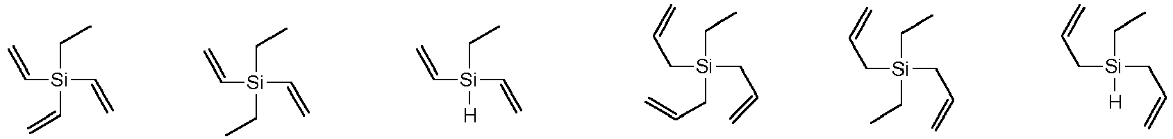
- the invention relates to a chemical precursor for forming a silicon containing film comprising at least two compounds wherein a first compound comprises at least one member selected from the group consisting of compounds having at least one carbon-carbon double bond or C-C triple bond wherein the compound is represented by the formula R 1 n SiR 4-n wherein R is selected from a linear or branched C 2 to C 6 alkenyl group, a linear or branched C 2 to C 6 alkynyl group; R 1 is selected from hydrogen and a branched C 1 to C 10 alkyl group; and n is a number selected from 0, 1, 2, and 3, and a second compound comprise at least one member selected from the group consisting of the following Formulae:
- the method and compounds described herein comprises at least two silicon precursor compounds: an at least one first compound and at least one second compound.
- compositions comprising at least two precursor compounds and methods using same to deposit a flowable film via a chemical vapor deposition (CVD) process on at least a portion of a substrate having a surface feature.
- CVD chemical vapor deposition
- Films deposited by, for example, flowable chemical deposition treatment experience film shrinkage during post-treatment due to the low process temperature. Voids and seams can form in the film due to significant film shrinkage and the increase of film stress. Thus, it has been challenging to densify the film without increasing film stress or creating voids.
- the composition and method described herein overcomes these problems by improving the fill of at least a portion of a surface feature on a substrate by using the co-deposition of at least two precursor compounds.
- an increased amount of cross-linking can be generated by using a first compound containing unsaturated carbon bonds which break and at least partially react with a second compound having at least one Si-H bond.
- the reaction may happen during the deposition step, the treatment step, or both the deposition and treatment step.
- the improvement in cross-linking reduces the voids in the gap fill which can arise during the treatment step (e.g., thermal annealing and/or UV cure).
- the method and compounds described herein comprises at least two silicon precursor compounds: an at least one first compound having an unsaturated carbon bond (e.g., a carbon-carbon double bond or a carbon-carbon triple bond) and at least one second compound having at least one Si-H bond.
- an unsaturated carbon bond e.g., a carbon-carbon double bond or a carbon-carbon triple bond
- second compound having at least one Si-H bond
- the first compound is a compound having at least one carbon-carbon double bond or C-C triple bond wherein the compound is represented by the formula R 1 n SiR 4-n wherein R is selected from a linear or branched C 2 to C 6 alkenyl group, a linear or branched C 2 to C 6 alkynyl group; R 1 is selected from hydrogen and a branched C 1 to C 10 alkyl group; and n is a number selected from 0, 1, 2, and 3.
- Exemplary compounds for Formula I include, but not limited to, the following:
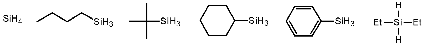
- the second compound is a compound comprising at least one Si-H bond and is at least one selected from the group consisting of the following Formulae IIA to IIH and IIIA:
- Exemplary compounds for Formula IIA include, but not limited to, disilane, trisilane, tetrasilane, pentasilane, hexasilane, and combinations thereof.
- Exemplary compounds for Formula IIB include, but not limited to, the following:
- Exemplary compounds for Formula IIC include, but not limited to, the following:
- Exemplary compounds for Formula IID include, but not limited to, the following:
- Exemplary compounds for Formula IIE include, but not limited to, the following:
- Exemplary compounds for Formula IIF include, but not limited to, the following:
- Exemplary compounds for Formula IIG include, but not limited to, the following:
- Exemplary compounds for Formula IIH include, but not limited to, the following:
- Exemplary compounds for Formula IIIA include, but not limited to, the following:
- linear or branched alkyl denotes a linear functional group having from 1 to 10, 3 to 10, or 1 to 6 carbon atoms.
- branched alkyl denotes a linear functional group having from 3 to 10, or 1 to 6 carbon atoms.
- Exemplary linear or branched alkyl groups include, but are not limited to, methyl (Me), ethyl (Et), isopropyl (Pr i ), isobutyl (Bu i ), sec-butyl (Bu s ), tert-butyl (Bu t ), iso-pentyl, tert-pentyl (am), isohexyl, and neohexyl.
- the alkyl group may have one or more functional groups such as, but not limited to, an alkoxy group, a dialkylamino group or combinations thereof, attached thereto. In other embodiments, the alkyl group does not have one or more functional groups attached thereto.
- the alkyl group may be saturated or, alternatively, unsaturated.
- cyclic alkyl denotes a cyclic group having from 3 to 10 or 5 to 10 atoms.
- exemplary cyclic alkyl groups include, but are not limited to, cyclobutyl, cyclopentyl, cyclohexyl, and cyclooctyl groups.
- the cyclic alkyl group may have one or more C 1 to C 10 linear, branched substituents, or substituents containing oxygen or nitrogen atoms.
- the cyclic alkyl group may have one or more linear or branched alkyls or alkoxy groups as substituents, such as, for example, a methylcyclohexyl group or a methoxycyclohexyl group.
- aryl denotes an aromatic cyclic functional group having from 3 to 10 carbon atoms, from 5 to 10 carbon atoms, or from 6 to 10 carbon atoms.
- exemplary aryl groups include, but are not limited to, phenyl, benzyl, chlorobenzyl, tolyl, and o-xylyl.
- alkenyl group denotes a group which has one or more carbon-carbon double bonds and has from 2 to 12, from 2 to 10, or from 2 to 6 carbon atoms.
- alkenyl groups include, but are not limited to, vinyl or allyl groups.
- alkynyl group denotes a group which has one or more carbon-carbon triple bonds and has from 2 to 12 or from 2 to 6 carbon atoms.
- alkylene group denotes a group which is derived from an alkyl by removal of two hydrogen atoms.
- exemplary alkylene groups include, but are not limited to, methylene (-CH 2 -) or ethylene (-CH 2 CH 2 -) groups.
- the term "unsaturated” as used herein means that the functional group, substituent, ring or bridge has one or more carbon double or triple bonds.
- An example of an unsaturated ring can be, without limitation, an aromatic ring such as a phenyl ring.
- saturated means that the functional group, substituent, ring or bridge does not have one or more double or triple bonds.
- one or more of the alkyl group, alkenyl group, alkynyl group, aryl group, and/or cyclic alkyl group in the formulae may be "substituted" or have one or more atoms or group of atoms substituted in place of, for example, a hydrogen atom.
- substituents include, but are not limited to, oxygen, sulfur, halogen atoms (e.g., F, Cl, I, or Br), nitrogen, alkyl groups, and phosphorous.
- one or more of the alkyl group, alkenyl group, alkynyl group, aromatic and/or aryl group in the formulae may be unsubstituted.
- the ratio of the inventive first and second precursors can range from about 0:5 to about 2:1 and will vary as a function of the selected first and second precursor. In one aspect of the invention, increasing the ratio of TVS to TSA can be used to reduce voiding (or increasing the density).
- the silicon precursor compounds described herein may be delivered to the reaction chamber such as a CVD or ALD reactor in a variety of ways.
- a liquid delivery system may be utilized.
- a combined liquid delivery and flash vaporization process unit may be employed, such as, for example, the turbo vaporizer manufactured by MSP Corporation of Shoreview, MN, to enable low volatility materials to be volumetrically delivered, which leads to reproducible transport and deposition without thermal decomposition of the precursor.
- the precursors described herein may be delivered in neat liquid form, or alternatively, may be employed in solvent formulations or compositions comprising same.
- the precursor formulations may include solvent component(s) of suitable character as may be desirable and advantageous in a given end use application to form a film on a substrate.
- suitable solvents can comprise at least one member selected from the group consisting of non-polar alkane based solvents such as cyclohexane and cyclohexanone.
- the silicon precursor compounds are preferably substantially free of halide ions such as chloride or metal ions such as Al.
- halide ions such as, for example, chlorides and fluorides, bromides, iodides, Al 3+ ions, Fe 2+ , Fe 3+ , Ni 2+ , Cr 3+ means less than 5 ppm (by weight), preferably less than 3 ppm, and more preferably less than 1 ppm, and most preferably 0 ppm.
- Chlorides or metal ions are known to act as decomposition catalysts for silicon precursors. Significant levels of chloride in the final product can cause the silicon precursors to degrade.
- silicon precursors are known to form flammable and/or pyrophoric gases upon decomposition such as hydrogen and silane. Therefore, the accelerated decomposition of the silicon precursors presents safety and performance concerns related to the formation of these flammable and/or pyrophoric gaseous byproducts.
- the method used to form the films or coatings described herein are flowable chemical deposition processes.
- suitable deposition processes for the method disclosed herein include, but are not limited to, cyclic flowable chemical vapor deposition (CFCVD), or plasma enhanced flowable chemical vapor deposition (PEFCVD).
- CFCVD cyclic flowable chemical vapor deposition
- PEFCVD plasma enhanced flowable chemical vapor deposition
- the term "flowable chemical vapor deposition processes” refers to any process wherein a substrate is exposed to one or more volatile precursors, which react and/or decompose on the substrate surface to provide flowable oligomeric silicon-containing species and then produce the solid film or material upon further treatment and, in some cases at least a portion of the oligomeric species comprises polymeric species.
- the precursors, reagents and sources used herein may be sometimes described as "gaseous", it is understood that the precursors can be either liquid or solid which are transported with or without an inert gas into the reactor via direct vaporization, bubbling or sublimation.
- the vaporized precursors can pass through a plasma generator.
- the films are deposited using a plasma-based (e.g., remote generated or in situ) CVD process.
- reactor includes without limitation, a reaction chamber or deposition chamber.
- the compounds precursors with Formulae I and IIA-H may be delivered to the flowable chemical vapor deposition reactor in a variety of ways including but not limited to vapor draw, bubbling or direct liquid injection (DLI).
- a liquid delivery system may be utilized.
- reactor may be equipped with a dual plenum showerhead to keep the plasma species generated remotely separate from vapors of the precursors until they are combined in the reactor to deposit flowable liquid.
- a combined liquid delivery and flash vaporization process unit may be employed, such as, for example, the turbo vaporizer manufactured by MSP Corporation of Shoreview, MN, to enable low volatility materials to be volumetrically delivered, which leads to reproducible transport and deposition without thermal decomposition of the precursor.
- the precursors described herein may be delivered in neat liquid form, or alternatively, may be employed in solvent formulations or compositions comprising same.
- the precursor formulations may include solvent component(s) of suitable character as may be desirable and advantageous in a given end use application to form a film on a substrate.
- the two precursors with Formulae I and IIA-H can be delivered with different injection inlet to avoid reaction between the two precursors prior to entering reactor chamber.
- the two or more precursors with Formulae I and IIA-H can be pre-mixed if they are compatible and then delivered into the reactor chamber using DLI method.
- the substrate may be exposed to one or more pre-deposition treatments such as, but not limited to, a plasma treatment, thermal treatment, chemical treatment, ultraviolet light exposure, electron beam exposure, and combinations thereof to affect one or more properties of the films.
- pre-deposition treatments such as, but not limited to, a plasma treatment, thermal treatment, chemical treatment, ultraviolet light exposure, electron beam exposure, and combinations thereof to affect one or more properties of the films.
- These pre-deposition treatments may occur under an atmosphere selected from inert, oxidizing, and/or reducing.
- Energy is applied to the at least one of the compound, nitrogen-containing source, oxygen source, other precursors or combination thereof to induce reaction and to form the silicon-containing film or coating on the substrate.
- energy can be provided by, but not limited to, thermal, plasma, pulsed plasma, helicon plasma, high density plasma, inductively coupled plasma, X-ray, e-beam, photon, remote plasma methods, and combinations thereof.
- a secondary RF frequency source can be used to modify the plasma characteristics at the substrate surface.
- the plasma-generated process may comprise a direct plasma-generated process in which plasma is directly generated in the reactor, or alternatively a remote plasma-generated process in which plasma is generated outside of the reactor and supplied into the reactor.
- the method deposits a film upon at least a portion of the surface of a substrate comprising a surface feature.
- the substrate is placed into the reactor and the substrate is maintained at one or more temperatures ranging from below 100 °C, preferably at a temperature below 25 °C and most preferably below 10 °C and greater than - 20 °C.
- the substrate comprises one or more surface features.
- the surface feature(s) have a width of 1 ⁇ m in width or less, or 500 nm in width or less, or 50 nm in width or less, or 10 nm in width.
- the aspect ratio (the depth to width ratio) of the surface features, if present, is 0.1:1 or greater, or 1:1 or greater, or 10:1 or greater, or 20:1 or greater, or 40:1 or greater.
- the substrate may be a single crystal silicon wafer, a wafer of silicon carbide, a wafer of aluminum oxide (sapphire), a sheet of glass, a metallic foil, an organic polymer film or may be a polymeric, glass, silicon or metallic 3-dimensional article.
- the substrate may be coated with a variety of materials well known in the art including films of silicon oxide, silicon nitride, amorphous carbon, silicon oxycarbide, silicon oxynitride, silicon carbide, gallium arsenide, gallium nitride and the like. These coatings may completely coat the substrate, may be in multiple layers of various materials and may be partially etched to expose underlying layers of material.
- the surface may also have on it a photoresist material that has been exposed with a pattern and developed to partially coat the substrate.
- the substrate comprises at least one member selected from the group consisting of Si, SiO x , SiN, SiGe, SiOC and SiON.
- the inventive silicon containing film can be employed as a hard mask and provide etch selectivity to a photoresist.
- the inventive silicon containing film functions as a dielectric film between conductive materials, as a barrier between conductive and other dielectric, or as a film within a sandwich dielectric.
- the reactor is at a pressure below atmospheric pressure or 750 torr (10 5 Pascals (Pa)) or less, or 100 torr (13332 Pa) or less. In other embodiments, the pressure of the reactor is maintained at a range of about 0.1torr (13 Pa) to about 10 torr (1333 Pa).
- the introducing step, wherein the at least one compound and a plasma are introduced into the reactor, is conducted at one or more temperatures ranging from below 100 °C, preferably at a temperature below 25 °C and most preferably below 10 °C and greater than -20 °C.
- the substrate comprises a semiconductor substrate comprising a surface feature.
- the plasma comprising nitrogen can be selected from the group consisting of nitrogen plasma, nitrogen/hydrogen plasma, nitrogen/helium plasma, nitrogen/argon plasma, ammonia plasma, ammonia/helium plasma, ammonia/argon plasma, ammonia/nitrogen plasma, NF 3 , NF 3 plasma, organic amine plasma, and mixtures thereof.
- the at least one compound and nitrogen source react and form a silicon nitride film (which is non-stoichiometric) or a silicon carbonitride film on at least a portion of the surface feature and substrate.
- organic amine as used herein describes an organic compound that has at least one nitrogen atom.
- organoamine examples include methylamine, ethylamine, propylamine, iso-propylamine, tert-butylamine, sec-butylamine, tert-amylamine, ethylenediamine, dimethylamine, trimethylamine, diethylamine, pyrrole, 2,6-dimethylpiperidine, di-n-propylamine, di-iso-propylamine, ethylmethylamine, N-methylaniline, pyridine, and triethylamine.
- the plasma source is selected from but not limited to the group consisting of a carbon source plasma, including a hydrocarbon plasma, a plasma comprising hydrocarbon and helium, a plasma comprising hydrocarbon and argon, carbon dioxide plasma, carbon monoxide plasma, a plasma comprising hydrocarbon and hydrogen, a plasma comprising hydrocarbon and a nitrogen source, a plasma comprising hydrocarbon and an oxygen source, and mixture thereof.
- the at least one compound and carbon source react and form a silicon carbide film (which is non-stoichiometric), or a silicon carbonitride film, or a silicon oxynitride film, or a silicon oxycarbide film, or a silicon oxycarbonitrde film on at least a portion of the surface feature and substrate.
- the plasma source is selected from but not limited to hydrogen plasma, helium plasma, argon plasma, xenon plasma, and mixture thereof.
- the at least one compound and plasma react and form a silicon nitride film, or a silicon carbide film, or a silicon carbonitride film on at least a portion of the surface feature and substrate.
- the substrate is optionally treated with an oxygen-containing source under certain process conditions sufficient to make the silicon nitride film form a silicon oxide or a silicon oxynitride or carbon doped silicon oxide film.
- the oxygen-containing source can be selected from the group consisting of water (H 2 O), oxygen (O 2 ), oxygen plasma, ozone (O 3 ), NO, N 2 O, carbon monoxide (CO), carbon dioxide (CO 2 ), N 2 O plasma, carbon monoxide (CO) plasma, carbon dioxide (CO 2 ) plasma, and combinations thereof.
- the flowable oligomer is treated at one or more temperatures ranging from about 100 °C to about 1000 °C to densify at least a portion of the materials.
- the post thermal treatment materials are exposed to a plasma, infrared lights, chemical treatment, an electron beam, or UV light to form a dense film.
- steps of the methods described herein may be performed in a variety of orders, may be performed sequentially or concurrently (e.g., during at least a portion of another step), and any combination thereof.
- the respective step of supplying the compounds and other reagents may be performed by varying the duration of the time for supplying them to change the stoichiometric composition of the resulting silicon-containing film.
- a method for depositing a silicon-containing film comprising:
- the plasma comprising nitrogen can be selected from the group consisting of nitrogen plasma, nitrogen/hydrogen plasma, nitrogen/helium plasma, nitrogen/argon plasma, ammonia plasma, ammonia/helium plasma, ammonia/argon plasma, ammonia/nitrogen plasma, NF 3 , NF 3 plasma, organic amine plasma, and mixtures thereof.
- the plasma source is selected from but not limited to the group consisting of a carbon source plasma, including a hydrocarbon plasma, a plasma comprising hydrocarbon and helium, a plasma comprising hydrocarbon and argon, carbon dioxide plasma, carbon monoxide plasma, a plasma comprising hydrocarbon and hydrogen, a plasma comprising hydrocarbon and a nitrogen source, a plasma comprising hydrocarbon and an oxygen source, and mixture thereof.
- a carbon source plasma including a hydrocarbon plasma, a plasma comprising hydrocarbon and helium, a plasma comprising hydrocarbon and argon, carbon dioxide plasma, carbon monoxide plasma, a plasma comprising hydrocarbon and hydrogen, a plasma comprising hydrocarbon and a nitrogen source, a plasma comprising hydrocarbon and an oxygen source, and mixture thereof.
- the plasma source is selected from but not limited to hydrogen plasma, helium plasma, argon plasma, xenon plasma, and mixture thereof.
- the at least one compound and plasma react and form a silicon nitride film, or a silicon carbide film, or a silicon carbonitride film on at least a portion of the surface feature and substrate.
- the substrate is optionally treated with an oxygen-containing source under certain process conditions sufficient to make the silicon nitride film form a silicon oxide or a silicon oxynitride or carbon doped silicon oxide film.
- the oxygen-containing source can be selected from the group consisting of water (H 2 O), oxygen (O 2 ), oxygen plasma, ozone (O 3 ), NO, N 2 O, carbon monoxide (CO), carbon dioxide (CO 2 ), N 2 O plasma, carbon monoxide (CO) plasma, carbon dioxide (CO 2 ) plasma, and combinations thereof.
- the flowable oligomer is treated at one or more temperatures ranging from about 100 °C to about 1000 °C to density at least a portion of the materials.
- the post thermal treatment materials are exposed to a plasma, infrared lights, chemical treatment, an electron beam, or UV light to form a dense film.
- a post treatment comprising exposure to UV light exposure is conducted under conditions to emit ethylene and silane gaseous by-products.
- FCVD Flowable chemical vapor deposition
- Depositions on a modified FCVD chamber on an Applied Materials Precision 5000 system can be performed using either a silane or a TEOS process kit.
- the chamber has direct liquid injection (DLI) delivery capability.
- the precursors are liquids with delivery temperatures dependent on the precursor's boiling point.
- typical liquid precursor flow rates were 100-5000 mg/min, in-situ plasma power density was 0.25 - 3.5 W/cm 2 , pressure was 0.75 - 12 Torr.
- the films were thermally annealed and/or UV cured in vacuum using the modified PECVD chamber at 100 ⁇ 1000 °C, preferably 300 ⁇ 400 °C.
- Thickness and refractive index (RI) at 632 nm were measured by a SCI reflectometer or Woollam ellipsometer. Typical film thickness ranged from 10 to 2000 nm. Bonding properties and hydrogen content (Si-H, C-H and N-H) of the silicon-based films were measured and analyzed by a Nicolet transmission Fourier transform infrared spectroscopy (FTIR) tool. All density measurements were accomplished using X-ray reflectivity (XRR). X-ray Photoelectron Spectroscopy (XPS) and Secondary ion mass spectrometry (SIMS) analysis were performed to determine the elemental composition of the films. The flowability and gap fill effects on patterned wafers were observed by a cross-sectional Scanning Electron Microscopy (SEM) using a Hitachi S-4700 system at a resolution of 2.0 nm.
- SEM cross-sectional Scanning Electron Microscopy
- Flowable CVD depositions were conducted using a design of experiment (DOE) methodology.
- the experimental design includes: two precursor flows from 100 to 5000 mg/min, preferably 500 to 2000 mg/min; NH 3 flow from 0 sccm to 1000 sccm, preferably 0 to 500 sccm; pressure from 0.75 to 12 Torr, preferably 6 to 10 Torr; RF power (13.56 MHz) 50 to 1000 W, preferably 100 ⁇ 500 W; Low-frequency (LF) power 0 to 100 W; and deposition temperature ranged from -20 to 40°C.
- DOE design of experiment
- Example 1 Deposition of flowable silicon carbide films using tetravinylsilane (TVS, Formula I) and 1,4-disilabutane (DSB, Formula IID)
- the flowable film was thermally annealed at 300°C for 5 min, followed by 400°C UV cure for 1, 3, 5 and 10 minutes. The refractive index and film density increased with the UV treatment time.
- Cross-sectional SEM indicates that bottom-up, seamless and void-free gap-fill was achieved by the co-deposition of the precursor compounds TVS and 1,4-disilabutane, as shown in Figure 1 (a) and Figure 1 (b) .
- the film was thermally annealed for 5 min at 300 °C and UV cured for 1 min at 400 °C.
- the flowable SiC film showed good stability by ambient exposure. Stability is measured by detecting changes to film thickness (e.g., as measured by refractive index) wherein a film with poor stability has a reduced thickness by being oxidized when exposed to ambient moisture and oxygen levels. There was no change in thickness or refractive index.
- Example 2 Deposition of flowable silicon carbonitride films using tetravinylsilane (TVS, Formula I) and trisilylamine (TSA, Formula IIG)
- the flowable film was thermally annealed at 300°C for 5 min, followed by 400°C UV cure for 1, 3, 5 and 10 minutes. The refractive index and film density increase with the UV time.
- Cross-sectional SEM indicates that bottom-up, seamless and void-free gap-fill was achieved by the co-deposition of a first precursor TVS and second precursor TSA, as shown in Figure 2 (a) and Figure 2 (b) .
- the film was thermally annealed at 300 °C for 5 min and UV cured at 400 °C for 10 min.
- the flowable SiCN film showed good stability by ambient exposure. There was no change in thickness or refractive index.
- the WER was also tested by dipping the film into dilute HF solutions.
- the flowable SiCN films showed etch resistance of HF solutions.
- Example 3 Deposition of flowable silicon carbonitride films using tetravinylsilane (TVS, Formula I) and trisilylamine (TSA, Formula IIG) by a cyclic process
- Example 4 Deposition of flowable silicon carbonitride films using tetravinylsilane (TVS, Formula I) and di-iso-propylaminosilane (DIPAS, Formula IIE)
- TVS tetravinylsilane
- DIPAS di-iso-propylaminosilane
- Example 5 Deposition of flowable silicon carbonitride films using trivinylmethylsilane (TVMS, Formula I) and trisilylamine (TSA, Formula IIG)
- Example 6 Deposition of flowable silicon carbonitride films using trivinylmethylsilane (TVMS, Formula I) and 1,4-disilabutane (DSB, Formula IIC)
- Example 7 Deposition of flowable silicon carbonitride films using tetravinylsilane (TVS, Formula I) and N,N'-disilyltrisilazane (Formula IIG)
- Cross-sectional SEM indicates that bottom-up, seamless and void-free gap-fill was achieved by the co-deposition of a first precursor TVS and second precursor TSA dimer, as shown in Figure 7 . Comparing to the combination of TVS and TSA, the combination of TVS and TSA dimer demonstrated higher film density (>1.8 g/cm 3 ), higher N content (18 ⁇ 19%) and lower C content (36 ⁇ 37%).
- Example 8 Deposition of flowable silicon carbonitride films using tetravinylsilane (TVS, Formula I) and di-iso-propylaminodisilane (DIPADS, Formula IIIA)
Landscapes
- Chemical & Material Sciences (AREA)
- Engineering & Computer Science (AREA)
- Organic Chemistry (AREA)
- Chemical Kinetics & Catalysis (AREA)
- General Chemical & Material Sciences (AREA)
- Materials Engineering (AREA)
- Mechanical Engineering (AREA)
- Metallurgy (AREA)
- Inorganic Chemistry (AREA)
- Physics & Mathematics (AREA)
- Plasma & Fusion (AREA)
- Chemical Vapour Deposition (AREA)
- Formation Of Insulating Films (AREA)
- Silicon Compounds (AREA)
- Prostheses (AREA)
- Silicon Polymers (AREA)
Claims (12)
- Verfahren zum Abscheiden eines siliziumhaltigen Films in einem fließfähigen chemischen Dampfabscheidungsprozess, das Verfahren umfassend:Einbringen eines Substrats, welches ein Oberflächenmerkmal aufweist, in einen Reaktor, wobei sich das Substrat bei einer oder mehreren Temperaturen im Bereich von mehr als -20°C bis unter 100°C befindet;Einführen einer ersten Verbindung mit mindestens einer Kohlenstoff-Kohlenstoff-Doppelbindung oder Kohlenstoff-Kohlenstoff-Dreifachbindung in den Reaktor, wobei die erste Verbindung die Formel R1 nSiR4-n hat, in der R ausgewählt ist aus einer linearen oder verzweigten C2- bis C6-Alkenylgruppe, einer linearen oder verzweigten C2- bis C6-Alkinylgruppe; R1 ausgewählt ist aus Wasserstoff und einer verzweigten C1- bis C10-Alkylgruppe; und n eine Zahl ist, die ausgewählt ist aus 0, 1, 2 und 3;Einführen einer zweiten Verbindung mit mindestens einer Si-H-Bindung in den Reaktor, wobei die zweite Verbindung ausgewählt ist aus der Gruppe bestehend aus den folgenden Formeln IIA bis IIH und IIIA:IIA. eine Polysilanverbindung mit der Formel SixH2x+2, worin x eine Zahl von 2 bis 6 ist;IIB. eine Verbindung mit der Formel R1 mSiH4-m, worin R1 ausgewählt ist aus Wasserstoff und einer linearen oder verzweigten C1- bis C10-Alkylgruppe; und m eine Zahl ist, ausgewählt aus 1, 2 und 3;IIC. eine Verbindung mit der Formel SiH3-R2-SiH3, worin R2 eine lineare oder verzweigte C1- bis C6-Alkylengruppe ist;IID. eine Verbindung mit der Formel R3SiH2-R2-SiH2R4, worin R2 eine lineare oder verzweigte C1- bis C6-Alkylengruppe ist; R3 ausgewählt ist aus Wasserstoff, einer linearen oder verzweigten C1- bis C10-Alkylgruppe und einer C4- bis C10-Arylgruppe; und R4 ausgewählt ist aus einer linearen oder verzweigten C1- bis C10-Alkylgruppe;IIE. eine Verbindung mit der Formel (R3R4N)nSiH3-nR1, worin R1 ausgewählt ist aus Wasserstoff und einer linearen oder verzweigten C1- bis C10-Alkylgruppe; R3 ausgewählt ist aus Wasserstoff, einer linearen oder verzweigten C1- bis C10-Alkylgruppe und einer C4- bis C10-Arylgruppe; und R4 ausgewählt ist aus einer linearen oder verzweigten C1- bis C10-Alkylgruppe;IIF. eine Silacycloalkylverbindung;IIG. eine Trisilylaminverbindung oder Derivate davon; undIIH. eine Silazanverbindung mit der Formel [(R3R4N)pSiH3-p]2NR1 oder [R3 pSiH2. pNR1]q, worin R1 ausgewählt ist aus Wasserstoff und einer linearen oder verzweigten C1- bis C10-Alkylgruppe; R3 ausgewählt ist aus Wasserstoff, einer linearen oder verzweigten C1- bis C10-Alkylgruppe und einer C4- bis C10-Arylgruppe; und R4 ausgewählt ist aus einer linearen oder verzweigten C1- bis C10-Alkylgruppe; p=0, 1, 2; q=2 oder 3; undIIIA. ein Organoaminodisilan mit der Formel (R3R4N)SiH2SiH3, worin R3 aus Wasserstoff, einer verzweigten C1- bis C10-Alkylgruppe und einer C4- bis C10-Arylgruppe ausgewählt ist und R4 aus einer linearen oder verzweigten C1- bis C10-Alkylgruppe ausgewählt ist;undBereitstellen einer Plasmaquelle in dem Reaktor, um die erste und die zweite Verbindung zumindest teilweise umzusetzen, um ein fließfähiges Oligomer zu bilden, wobei das fließfähige Oligomer zumindest teilweise einen Teil des Oberflächenmerkmals ausfüllt.
- Das Verfahren nach Anspruch 1, wobei der Bereitstellungsschritt eine Stickstoff enthaltende Plasmaquelle umfasst, die ausgewählt ist aus der Gruppe bestehend aus Stickstoffplasma, einem Plasma, das Stickstoff und Wasserstoff enthält, einem Plasma, das Stickstoff und Helium enthält, einem Plasma, das Stickstoff und Argon enthält, Ammoniakplasma, einem Plasma, das Ammoniak und Helium enthält, ein Plasma, das Ammoniak und Argon enthält, ein Plasma, das Ammoniak und Stickstoff enthält, NF3, NF3-Plasma, organisches Aminplasma und Mischungen davon oder eine Plasmaquelle, die ausgewählt ist aus, aber nicht beschränkt ist auf die Gruppe, bestehend aus einem Kohlenstoffquellenplasma, einschließlich einem Kohlenwasserstoffplasma, einem Plasma, das Kohlenwasserstoff und Helium enthält, einem Plasma, das Kohlenwasserstoff und Argon umfasst, Kohlendioxidplasma, Kohlenmonoxidplasma, einem Plasma, das Kohlenwasserstoff und Wasserstoff umfasst, einem Plasma, das Kohlenwasserstoff und eine Stickstoffquelle umfasst, einem Plasma, das Kohlenwasserstoff und eine Sauerstoffquelle umfasst, und Mischungen davon, oder die Plasmaquelle ist ausgewählt aus, aber nicht beschränkt auf Wasserstoffplasma, Heliumplasma, Argonplasma, Xenonplasma und Mischungen davon, oder die Sauerstoff enthaltende Plasmaquelle ist ausgewählt aus der Gruppe bestehend aus Wasser (H2O)-Plasma, Sauerstoffplasma, Ozon (O3)-Plasma, NO-Plasma, N2O-Plasma, Kohlenmonoxid (CO)-Plasma, Kohlendioxid (CO2)-Plasma und Kombinationen davon.
- Das Verfahren nach den vorhergehenden Ansprüchen ferner umfassend die Behandlung des fließfähigen Oligomers bei einer oder mehreren Temperaturen im Bereich von 100 °C bis 1000 °C, um mindestens einen Teil der Materialien zu verdichten.
- Das Verfahren nach Anspruch 3, wobei die Materialien nach der thermischen Behandlung einem Plasma, Infrarotlicht, einer chemischen Behandlung, einem Elektronenstrahl oder UV-Licht ausgesetzt werden, um einen dichten Film zu bilden.
- Das Verfahren nach den vorhergehenden Ansprüchen, wobei der Abscheidungsprozess eine plasmaunterstützte chemische Gasphasenabscheidung ist und das Plasma in situ erzeugt wird oder das Plasma aus der Ferne erzeugt wird.
- Das Verfahren nach einem der vorhergehenden Ansprüche, bei dem der Druck im Reaktor auf 100 Torr oder weniger gehalten wird.
- Das Verfahren nach den vorhergehenden Ansprüchen, bei dem der siliciumhaltige Film ausgewählt ist aus der Gruppe bestehend aus Siliciumcarbid, Siliciumnitrid, kohlenstoffdotiertem Siliciumnitrid.
- Das Verfahren nach einem der Ansprüche 2 bis 6, wobei der siliziumhaltige Film ausgewählt ist aus der Gruppe bestehend aus Siliziumoxid, kohlenstoffdotiertem Siliziumoxid, Siliziumoxynitrid und kohlenstoffdotiertem Siliziumoxynitridfilm.
- Chemischer Vorläufer zur Bildung eines siliciumhaltigen Films, mindestens zwei Verbindungen umfassend, wobei eine erste Verbindung mindestens ein Mitglied umfasst, das aus der Gruppe ausgewählt ist, die aus Verbindungen mit mindestens einer Kohlenstoff-Kohlenstoff-Doppelbindung oder C-C-Dreifachbindung besteht, wobei die Verbindung durch die Formel R1 nSiR4-n dargestellt wird, worin R aus einer linearen oder verzweigten C2- bis C6-Alkenylgruppe, einer linearen oder verzweigten C2- bis C6-Alkinylgruppe ausgewählt ist; R1 ausgewählt ist aus Wasserstoff und einer verzweigten C1-bis C10-Alkylgruppe; und n eine Zahl ist, die aus 0, 1, 2 und 3 ausgewählt ist, und eine zweite Verbindung, mindestens ein Mitglied umfassend, das aus der Gruppe ausgewählt ist, die aus den folgenden Formeln besteht:IIB. eine Verbindung mit der Formel R1 mSiH4-m, worin R1 aus einer linearen oder verzweigten C1- bis C10-Alkylgruppe ausgewählt ist; und m eine Zahl ist, die aus 1, 2 und 3 ausgewählt ist;IIC. eine Verbindung mit der Formel SiH3-R2-SiH3, worin R2 eine lineare oder verzweigte C1- bis C6-Alkylengruppe ist;IID. eine Verbindung mit der Formel R3SiH2-R2-SiH2R4, worin R2 eine lineare oder verzweigte C1- bis C6-Alkylengruppe ist; R3 ausgewählt ist aus Wasserstoff, einer linearen oder verzweigten C1- bis C10-Alkylgruppe und einer C4- bis C10-Arylgruppe; und R4 ausgewählt ist aus einer linearen oder verzweigten C1- bis C10-Alkylgruppe;IIE. eine Verbindung mit der Formel (R3R4N)nSiH3-nR1, worin R1 ausgewählt ist aus Wasserstoff und einer verzweigten C1- bis C10-Alkylgruppe; R3 ausgewählt ist aus Wasserstoff, einer linearen oder verzweigten C1- bis C10-Alkylgruppe und einer C4- bis C10-Arylgruppe; und R4 ausgewählt ist aus einer linearen oder verzweigten C1- bis C10-Alkylgruppe;IIF. eine Silacycloalkylverbindung;IIG. eine Trisilylaminverbindung oder Derivate davon;IIH. eine Silazanverbindung mit der Formel [(R3R4N)pSiH3-p]2NR1 oder [R3 pSiH2. pNR1]q, worin R1 ausgewählt ist aus Wasserstoff und einer linearen oder verzweigten C1- bis C10-Alkylgruppe; R3 ausgewählt ist aus Wasserstoff, einer linearen oder verzweigten C1- bis C10-Alkylgruppe und einer C4- bis C10-Arylgruppe; und R4 ausgewählt ist aus einer linearen oder verzweigten C1- bis C10-Alkylgruppe; p=0, 1, 2; q=2 oder 3; undIIIA. ein Organoaminodisilan mit der Formel (R3R4N)SiH2SiH3, worin R3 ausgewählt ist aus Wasserstoff, einer verzweigten C1- bis C10-Alkylgruppe und einer C4- bis C10-Arylgruppe; und R4 ausgewählt ist aus einer linearen oder verzweigten C1- bis C10-Alkylgruppe.
- Der chemische Vorläufer der Formel IIIA der vorhergehenden Ansprüche, wobei R3 und R4 zu einem Ring verbunden sind.
- Der chemische Vorläufer nach einem der vorhergehenden Ansprüche, wobei die erste Verbindung mindestens einen Bestandteil umfasst, der ausgewählt ist aus der Gruppe bestehend aus:


- Der chemische Vorläufer nach einem der vorhergehenden Ansprüche, wobei die zweite Verbindung mindestens ein Mitglied aus der Gruppe bestehend aus Disilan, Trisilan, Tetrasilan, Pentasilan, Hexasilan und Kombinationen davon umfasst oder die zweite Verbindung umfasst mindestens ein Mitglied aus der Gruppe bestehend aus
 oder die zweite Verbindung umfasst mindestens ein Mitglied aus der Gruppe, bestehend aus:
 oder die zweite Verbindung umfasst mindestens ein Mitglied aus der Gruppe, bestehend aus:
 oder die zweite Verbindung umfasst mindestens ein Mitglied aus der Gruppe, bestehend aus:
 oder die zweite Verbindung umfasst mindestens ein Mitglied aus der Gruppe, bestehend aus:
 oder die zweite Verbindung umfasst mindestens ein Mitglied aus der Gruppe, bestehend aus:
 oder die zweite Verbindung umfasst mindestens ein Mitglied aus der Gruppe, bestehend aus:
 oder die zweite Verbindung umfasst mindestens ein Mitglied aus der Gruppe, bestehend aus:
Applications Claiming Priority (2)
| Application Number | Priority Date | Filing Date | Title |
|---|---|---|---|
| US201662300312P | 2016-02-26 | 2016-02-26 | |
| PCT/US2017/018873 WO2017147150A1 (en) | 2016-02-26 | 2017-02-22 | Compositions and methods using same for deposition of silicon-containing film |
Publications (3)
| Publication Number | Publication Date |
|---|---|
| EP3420117A1 EP3420117A1 (de) | 2019-01-02 |
| EP3420117A4 EP3420117A4 (de) | 2020-01-15 |
| EP3420117B1 true EP3420117B1 (de) | 2024-04-24 |
Family
ID=59685564
Family Applications (1)
| Application Number | Title | Priority Date | Filing Date |
|---|---|---|---|
| EP17757122.1A Active EP3420117B1 (de) | 2016-02-26 | 2017-02-22 | Zusammensetzungen und verfahren mit verwendung davon zur abscheidung von siliciumhaltigem film |
Country Status (9)
| Country | Link |
|---|---|
| US (1) | US12428722B2 (de) |
| EP (1) | EP3420117B1 (de) |
| JP (1) | JP6777754B2 (de) |
| KR (2) | KR102482618B1 (de) |
| CN (2) | CN109072426B (de) |
| IL (1) | IL261283B2 (de) |
| SG (1) | SG11201807211XA (de) |
| TW (2) | TWI773002B (de) |
| WO (1) | WO2017147150A1 (de) |
Families Citing this family (35)
| Publication number | Priority date | Publication date | Assignee | Title |
|---|---|---|---|---|
| US9257274B2 (en) | 2010-04-15 | 2016-02-09 | Lam Research Corporation | Gapfill of variable aspect ratio features with a composite PEALD and PECVD method |
| KR102326396B1 (ko) | 2013-09-27 | 2021-11-12 | 레르 리키드 쏘시에떼 아노님 뿌르 레드 에렉스뿔라따시옹 데 프로세데 조르즈 클로드 | 아민 치환된 트리실릴아민 및 트리디실릴아민 화합물 |
| SG11201703195QA (en) * | 2014-10-24 | 2017-05-30 | Versum Materials Us Llc | Compositions and methods using same for deposition of silicon-containing film |
| US11124876B2 (en) | 2015-03-30 | 2021-09-21 | L'Air Liquide, Société Anonyme pour l'Etude et l'Exploitation des Procédés Georges Claude | Si-containing film forming precursors and methods of using the same |
| US9777025B2 (en) | 2015-03-30 | 2017-10-03 | L'Air Liquide, Société pour l'Etude et l'Exploitation des Procédés Georges Claude | Si-containing film forming precursors and methods of using the same |
| US12221692B2 (en) | 2016-02-26 | 2025-02-11 | Versum Materials Us, Llc | Compositions and methods using same for deposition of silicon-containing film |
| JP6824717B2 (ja) * | 2016-12-09 | 2021-02-03 | 東京エレクトロン株式会社 | SiC膜の成膜方法 |
| US10192734B2 (en) * | 2016-12-11 | 2019-01-29 | L'Air Liquide, Société Anonyme pour l'Etude et l'Exploration des Procédés Georges Claude | Short inorganic trisilylamine-based polysilazanes for thin film deposition |
| IL273146B2 (en) * | 2017-09-14 | 2025-04-01 | Versum Mat Us Llc | Compositions and methods for depositing layers containing silicone |
| WO2019060069A1 (en) * | 2017-09-21 | 2019-03-28 | Applied Materials, Inc. | High aspect ratio deposition |
| JP6787875B2 (ja) * | 2017-12-20 | 2020-11-18 | 株式会社Kokusai Electric | 半導体装置の製造方法、基板処理装置、およびプログラム |
| CN112292479A (zh) * | 2018-06-11 | 2021-01-29 | 弗萨姆材料美国有限责任公司 | 用于沉积含硅膜的组合物及其使用方法 |
| US11373866B2 (en) * | 2018-06-29 | 2022-06-28 | Taiwan Semiconductor Manufacturing Co., Ltd. | Dielectric material and methods of forming same |
| US10985010B2 (en) * | 2018-08-29 | 2021-04-20 | Versum Materials Us, Llc | Methods for making silicon and nitrogen containing films |
| US11114306B2 (en) * | 2018-09-17 | 2021-09-07 | Applied Materials, Inc. | Methods for depositing dielectric material |
| JP2020136387A (ja) * | 2019-02-15 | 2020-08-31 | 東京エレクトロン株式会社 | 成膜方法、成膜処理用の処理容器のクリーニング方法及び成膜装置 |
| KR20240160679A (ko) | 2019-05-01 | 2024-11-11 | 램 리써치 코포레이션 | 변조된 원자 층 증착 |
| US20220234903A1 (en) * | 2019-05-24 | 2022-07-28 | Versum Materials Us, Llc | Organosilicon precursors for deposition of silicon-containing films |
| US12431349B2 (en) | 2019-06-07 | 2025-09-30 | Lam Research Corporation | In-situ control of film properties during atomic layer deposition |
| WO2021025874A1 (en) | 2019-08-06 | 2021-02-11 | Lam Research Corporation | Thermal atomic layer deposition of silicon-containing films |
| JP7246284B2 (ja) * | 2019-08-15 | 2023-03-27 | 東京エレクトロン株式会社 | 成膜方法 |
| US11499014B2 (en) | 2019-12-31 | 2022-11-15 | L'Air Liquide, Société Anonyme pour l'Etude et l'Exploitation des Procédés Georges Claude | Cureable formulations for forming low-k dielectric silicon-containing films using polycarbosilazane |
| CN115803474A (zh) | 2020-07-23 | 2023-03-14 | 朗姆研究公司 | 具有受控膜性质和高沉积速率的保形热cvd |
| KR20230043795A (ko) | 2020-07-28 | 2023-03-31 | 램 리써치 코포레이션 | 실리콘-함유 막들의 불순물 감소 |
| KR20220082751A (ko) * | 2020-12-09 | 2022-06-17 | 에이에스엠 아이피 홀딩 비.브이. | 실리콘-탄소 재료를 포함한 구조체를 형성하는 방법, 이 방법을 사용하여 형성된 구조체, 및 이 구조체를 형성하기 위한 시스템 |
| US11170994B1 (en) * | 2021-01-12 | 2021-11-09 | Applied Materials, Inc. | CD dependent gap fill and conformal films |
| US11355354B1 (en) * | 2021-01-25 | 2022-06-07 | Applied Materials, Inc. | Thermal deposition of doped silicon oxide |
| CN116918044A (zh) * | 2021-03-22 | 2023-10-20 | 株式会社国际电气 | 半导体装置的制造方法、基板处理方法、基板处理装置和程序 |
| US11970769B2 (en) * | 2021-06-24 | 2024-04-30 | Asm Ip Holding B.V. | Cyclical deposition methods |
| WO2023283144A1 (en) | 2021-07-09 | 2023-01-12 | Lam Research Corporation | Plasma enhanced atomic layer deposition of silicon-containing films |
| KR102901182B1 (ko) * | 2021-07-20 | 2025-12-16 | 에이에스엠 아이피 홀딩 비.브이. | 실리콘 카바이드 층을 포함한 구조체를 형성하는 방법 |
| TW202334501A (zh) * | 2022-01-03 | 2023-09-01 | 荷蘭商Asm Ip私人控股有限公司 | 沈積間隙填充流體之方法及相關系統與裝置 |
| WO2024112598A1 (en) * | 2022-11-22 | 2024-05-30 | Entegris, Inc. | Disilylamine precursors and related methods |
| CN121152793A (zh) * | 2023-05-25 | 2025-12-16 | Dnf有限公司 | 新颖的氨基烷氧基硅胺化合物、其制备方法及包括其的含硅薄膜沉积用组合物 |
| KR102904483B1 (ko) * | 2023-05-25 | 2025-12-29 | (주)디엔에프 | 신규한 아미노알콕시실릴아민 화합물, 이의 제조방법 및 이를 포함하는 실리콘 함유 박막증착용 조성물 |
Family Cites Families (48)
| Publication number | Priority date | Publication date | Assignee | Title |
|---|---|---|---|---|
| JPS61149226A (ja) | 1984-12-25 | 1986-07-07 | Agency Of Ind Science & Technol | ガス選択透過性複合膜およびその製造方法 |
| US6926926B2 (en) * | 2001-09-10 | 2005-08-09 | Applied Materials, Inc. | Silicon carbide deposited by high density plasma chemical-vapor deposition with bias |
| US7091137B2 (en) | 2001-12-14 | 2006-08-15 | Applied Materials | Bi-layer approach for a hermetic low dielectric constant layer for barrier applications |
| CN100567564C (zh) * | 2002-12-20 | 2009-12-09 | 应用材料有限公司 | 形成高质量的低温氮化硅层的方法和设备 |
| US6855645B2 (en) * | 2002-12-30 | 2005-02-15 | Novellus Systems, Inc. | Silicon carbide having low dielectric constant |
| JP4479190B2 (ja) * | 2003-08-22 | 2010-06-09 | 東ソー株式会社 | アルケニル基含有有機シラン化合物を含んでなる絶縁膜用材料、それを用いた絶縁膜および半導体デバイス |
| US20050109276A1 (en) * | 2003-11-25 | 2005-05-26 | Applied Materials, Inc. | Thermal chemical vapor deposition of silicon nitride using BTBAS bis(tertiary-butylamino silane) in a single wafer chamber |
| US7521378B2 (en) | 2004-07-01 | 2009-04-21 | Micron Technology, Inc. | Low temperature process for polysilazane oxidation/densification |
| US7438760B2 (en) | 2005-02-04 | 2008-10-21 | Asm America, Inc. | Methods of making substitutionally carbon-doped crystalline Si-containing materials by chemical vapor deposition |
| TWI263265B (en) * | 2005-02-13 | 2006-10-01 | United Microelectronics Corp | Method for fabricating ultra-high tensile-stressed film and strained-silicon transistors thereof |
| WO2006088015A1 (ja) * | 2005-02-18 | 2006-08-24 | Nec Corporation | 有機シリコン系膜の形成方法、当該有機シリコン系膜を有する半導体装置及びその製造方法 |
| US20060228903A1 (en) * | 2005-03-30 | 2006-10-12 | Mcswiney Michael L | Precursors for the deposition of carbon-doped silicon nitride or silicon oxynitride films |
| US20080124946A1 (en) * | 2006-11-28 | 2008-05-29 | Air Products And Chemicals, Inc. | Organosilane compounds for modifying dielectrical properties of silicon oxide and silicon nitride films |
| US7781352B2 (en) | 2007-06-06 | 2010-08-24 | Asm Japan K.K. | Method for forming inorganic silazane-based dielectric film |
| US7622162B1 (en) * | 2007-06-07 | 2009-11-24 | Novellus Systems, Inc. | UV treatment of STI films for increasing tensile stress |
| CN100590811C (zh) * | 2007-09-18 | 2010-02-17 | 上海华虹Nec电子有限公司 | 半导体晶圆制造中金属间介质填充方法 |
| US8987039B2 (en) * | 2007-10-12 | 2015-03-24 | Air Products And Chemicals, Inc. | Antireflective coatings for photovoltaic applications |
| US7943531B2 (en) * | 2007-10-22 | 2011-05-17 | Applied Materials, Inc. | Methods for forming a silicon oxide layer over a substrate |
| JP5304983B2 (ja) * | 2008-02-12 | 2013-10-02 | Jsr株式会社 | ケイ素含有膜形成用組成物 |
| JP5309619B2 (ja) * | 2008-03-07 | 2013-10-09 | ソニー株式会社 | 半導体装置およびその製造方法 |
| CN102318044A (zh) | 2008-05-08 | 2012-01-11 | 巴斯夫欧洲公司 | 包含碳化硅层的层型结构、其制备方法及其用途 |
| US20100081293A1 (en) | 2008-10-01 | 2010-04-01 | Applied Materials, Inc. | Methods for forming silicon nitride based film or silicon carbon based film |
| US8703624B2 (en) * | 2009-03-13 | 2014-04-22 | Air Products And Chemicals, Inc. | Dielectric films comprising silicon and methods for making same |
| US7825040B1 (en) | 2009-06-22 | 2010-11-02 | Asm Japan K.K. | Method for depositing flowable material using alkoxysilane or aminosilane precursor |
| US8541053B2 (en) | 2010-07-08 | 2013-09-24 | Molecular Imprints, Inc. | Enhanced densification of silicon oxide layers |
| US8460753B2 (en) * | 2010-12-09 | 2013-06-11 | Air Products And Chemicals, Inc. | Methods for depositing silicon dioxide or silicon oxide films using aminovinylsilanes |
| JP5731841B2 (ja) | 2011-02-02 | 2015-06-10 | 大陽日酸株式会社 | シリコン窒化膜の形成方法 |
| US8771807B2 (en) | 2011-05-24 | 2014-07-08 | Air Products And Chemicals, Inc. | Organoaminosilane precursors and methods for making and using same |
| EP3929326A3 (de) * | 2011-06-03 | 2022-03-16 | Versum Materials US, LLC | Zusammensetzungen und verfahren zur ablagerung von kohlenstoffdotierten siliciumhaltigen filmen |
| US20130217241A1 (en) | 2011-09-09 | 2013-08-22 | Applied Materials, Inc. | Treatments for decreasing etch rates after flowable deposition of silicon-carbon-and-nitrogen-containing layers |
| US20130217240A1 (en) * | 2011-09-09 | 2013-08-22 | Applied Materials, Inc. | Flowable silicon-carbon-nitrogen layers for semiconductor processing |
| US8753985B2 (en) | 2012-01-17 | 2014-06-17 | Applied Materials, Inc. | Molecular layer deposition of silicon carbide |
| US9200167B2 (en) * | 2012-01-27 | 2015-12-01 | Air Products And Chemicals, Inc. | Alkoxyaminosilane compounds and applications thereof |
| US8846536B2 (en) * | 2012-03-05 | 2014-09-30 | Novellus Systems, Inc. | Flowable oxide film with tunable wet etch rate |
| US8871656B2 (en) * | 2012-03-05 | 2014-10-28 | Applied Materials, Inc. | Flowable films using alternative silicon precursors |
| EP2823083B1 (de) * | 2012-03-09 | 2023-10-04 | Versum Materials US, LLC | Verfahren zur herstellung von silikonhaltigen filmen auf dünnfilmtransistorvorrichtungen |
| US20130243968A1 (en) | 2012-03-16 | 2013-09-19 | Air Products And Chemicals, Inc. | Catalyst synthesis for organosilane sol-gel reactions |
| US9117668B2 (en) * | 2012-05-23 | 2015-08-25 | Novellus Systems, Inc. | PECVD deposition of smooth silicon films |
| TWI449802B (zh) * | 2012-06-06 | 2014-08-21 | Univ Nat Chiao Tung | 掺碳氮化矽薄膜及其製造方法與裝置 |
| US9243324B2 (en) | 2012-07-30 | 2016-01-26 | Air Products And Chemicals, Inc. | Methods of forming non-oxygen containing silicon-based films |
| US8889566B2 (en) | 2012-09-11 | 2014-11-18 | Applied Materials, Inc. | Low cost flowable dielectric films |
| US10279959B2 (en) * | 2012-12-11 | 2019-05-07 | Versum Materials Us, Llc | Alkoxysilylamine compounds and applications thereof |
| US9343293B2 (en) * | 2013-04-04 | 2016-05-17 | Applied Materials, Inc. | Flowable silicon—carbon—oxygen layers for semiconductor processing |
| US9905415B2 (en) * | 2013-10-03 | 2018-02-27 | Versum Materials Us, Llc | Methods for depositing silicon nitride films |
| JP6206096B2 (ja) | 2013-10-31 | 2017-10-04 | 富士通株式会社 | 半導体装置の製造方法 |
| US20160079034A1 (en) * | 2014-09-12 | 2016-03-17 | Applied Materials Inc. | Flowable film properties tuning using implantation |
| US9777025B2 (en) | 2015-03-30 | 2017-10-03 | L'Air Liquide, Société pour l'Etude et l'Exploitation des Procédés Georges Claude | Si-containing film forming precursors and methods of using the same |
| JP2024149226A (ja) | 2023-04-07 | 2024-10-18 | キヤノン株式会社 | 画像形成装置 |
-
2017
- 2017-02-22 SG SG11201807211XA patent/SG11201807211XA/en unknown
- 2017-02-22 JP JP2018544903A patent/JP6777754B2/ja active Active
- 2017-02-22 KR KR1020217014935A patent/KR102482618B1/ko active Active
- 2017-02-22 EP EP17757122.1A patent/EP3420117B1/de active Active
- 2017-02-22 WO PCT/US2017/018873 patent/WO2017147150A1/en not_active Ceased
- 2017-02-22 IL IL261283A patent/IL261283B2/en unknown
- 2017-02-22 US US16/079,672 patent/US12428722B2/en active Active
- 2017-02-22 CN CN201780018637.5A patent/CN109072426B/zh active Active
- 2017-02-22 CN CN202111363990.1A patent/CN114231947A/zh active Pending
- 2017-02-22 KR KR1020187027630A patent/KR102255727B1/ko active Active
- 2017-02-23 TW TW109143007A patent/TWI773002B/zh active
- 2017-02-23 TW TW106106189A patent/TWI715732B/zh active
Also Published As
| Publication number | Publication date |
|---|---|
| KR20210060654A (ko) | 2021-05-26 |
| US12428722B2 (en) | 2025-09-30 |
| CN114231947A (zh) | 2022-03-25 |
| JP2019507956A (ja) | 2019-03-22 |
| KR20180114197A (ko) | 2018-10-17 |
| IL261283A (en) | 2018-10-31 |
| IL261283B2 (en) | 2025-02-01 |
| TW201742947A (zh) | 2017-12-16 |
| CN109072426B (zh) | 2021-12-03 |
| EP3420117A4 (de) | 2020-01-15 |
| TWI715732B (zh) | 2021-01-11 |
| CN109072426A (zh) | 2018-12-21 |
| JP6777754B2 (ja) | 2020-10-28 |
| KR102255727B1 (ko) | 2021-05-26 |
| TW202113124A (zh) | 2021-04-01 |
| EP3420117A1 (de) | 2019-01-02 |
| SG11201807211XA (en) | 2018-09-27 |
| WO2017147150A1 (en) | 2017-08-31 |
| KR102482618B1 (ko) | 2022-12-28 |
| IL261283B1 (en) | 2024-10-01 |
| TWI773002B (zh) | 2022-08-01 |
| US20190055645A1 (en) | 2019-02-21 |
Similar Documents
| Publication | Publication Date | Title |
|---|---|---|
| EP3420117B1 (de) | Zusammensetzungen und verfahren mit verwendung davon zur abscheidung von siliciumhaltigem film | |
| US12505999B2 (en) | Precursors and flowable CVD methods for making low-K films to fill surface features | |
| US20250188605A1 (en) | Compositions and Methods Using Same for Deposition of Silicon-Containing Film | |
| WO2017112732A1 (en) | Compositions and methods using same for deposition of silicon-containing film | |
| US20250215557A1 (en) | Compositions and methods using same for deposition of silicon-containing film | |
| US20210043446A1 (en) | Precursors and Flowable CVD Methods for Making Low-K Films to Fill Surface Features | |
| JP7485732B2 (ja) | 組成物、及びケイ素含有膜の堆積のための組成物を使用する方法 | |
| KR102870167B1 (ko) | 규소 함유 막의 증착을 위한 조성물 및 이의 사용 방법 |
Legal Events
| Date | Code | Title | Description |
|---|---|---|---|
| STAA | Information on the status of an ep patent application or granted ep patent |
Free format text: STATUS: THE INTERNATIONAL PUBLICATION HAS BEEN MADE |
|
| PUAI | Public reference made under article 153(3) epc to a published international application that has entered the european phase |
Free format text: ORIGINAL CODE: 0009012 |
|
| STAA | Information on the status of an ep patent application or granted ep patent |
Free format text: STATUS: REQUEST FOR EXAMINATION WAS MADE |
|
| 17P | Request for examination filed |
Effective date: 20180906 |
|
| AK | Designated contracting states |
Kind code of ref document: A1 Designated state(s): AL AT BE BG CH CY CZ DE DK EE ES FI FR GB GR HR HU IE IS IT LI LT LU LV MC MK MT NL NO PL PT RO RS SE SI SK SM TR |
|
| AX | Request for extension of the european patent |
Extension state: BA ME |
|
| RIN1 | Information on inventor provided before grant (corrected) |
Inventor name: LEI, XINJIAN Inventor name: XIAO, MANCHAO Inventor name: SINATORE, DINO Inventor name: RIDGEWAY, ROBERT, GORDON Inventor name: LI, JIANHENG Inventor name: VRTIS, RAYMOND, NICHOLAS |
|
| DAV | Request for validation of the european patent (deleted) | ||
| DAX | Request for extension of the european patent (deleted) | ||
| RIC1 | Information provided on ipc code assigned before grant |
Ipc: H01L 21/02 20060101ALI20190927BHEP Ipc: C23C 16/36 20060101ALI20190927BHEP Ipc: C23C 16/505 20060101ALI20190927BHEP Ipc: C23C 16/32 20060101AFI20190927BHEP Ipc: H01L 21/31 20060101ALI20190927BHEP |
|
| A4 | Supplementary search report drawn up and despatched |
Effective date: 20191213 |
|
| RIC1 | Information provided on ipc code assigned before grant |
Ipc: C23C 16/505 20060101ALI20191209BHEP Ipc: C23C 16/36 20060101ALI20191209BHEP Ipc: H01L 21/31 20060101ALI20191209BHEP Ipc: C23C 16/32 20060101AFI20191209BHEP Ipc: H01L 21/02 20060101ALI20191209BHEP |
|
| STAA | Information on the status of an ep patent application or granted ep patent |
Free format text: STATUS: EXAMINATION IS IN PROGRESS |
|
| 17Q | First examination report despatched |
Effective date: 20220131 |
|
| REG | Reference to a national code |
Free format text: PREVIOUS MAIN CLASS: C23C0016320000 Ref country code: DE Ref legal event code: R079 Ref document number: 602017081283 Country of ref document: DE Free format text: PREVIOUS MAIN CLASS: C23C0016320000 Ipc: C23C0016040000 |
|
| RIC1 | Information provided on ipc code assigned before grant |
Ipc: H01L 21/02 20060101ALI20230519BHEP Ipc: C23C 16/56 20060101ALI20230519BHEP Ipc: C23C 16/505 20060101ALI20230519BHEP Ipc: C23C 16/46 20060101ALI20230519BHEP Ipc: C23C 16/455 20060101ALI20230519BHEP Ipc: C23C 16/40 20060101ALI20230519BHEP Ipc: C23C 16/36 20060101ALI20230519BHEP Ipc: C23C 16/34 20060101ALI20230519BHEP Ipc: C23C 16/32 20060101ALI20230519BHEP Ipc: C23C 16/30 20060101ALI20230519BHEP Ipc: C23C 16/04 20060101AFI20230519BHEP |
|
| P01 | Opt-out of the competence of the unified patent court (upc) registered |
Effective date: 20230602 |
|
| GRAP | Despatch of communication of intention to grant a patent |
Free format text: ORIGINAL CODE: EPIDOSNIGR1 |
|
| STAA | Information on the status of an ep patent application or granted ep patent |
Free format text: STATUS: GRANT OF PATENT IS INTENDED |
|
| INTG | Intention to grant announced |
Effective date: 20231204 |
|
| GRAS | Grant fee paid |
Free format text: ORIGINAL CODE: EPIDOSNIGR3 |
|
| GRAA | (expected) grant |
Free format text: ORIGINAL CODE: 0009210 |
|
| STAA | Information on the status of an ep patent application or granted ep patent |
Free format text: STATUS: THE PATENT HAS BEEN GRANTED |
|
| AK | Designated contracting states |
Kind code of ref document: B1 Designated state(s): AL AT BE BG CH CY CZ DE DK EE ES FI FR GB GR HR HU IE IS IT LI LT LU LV MC MK MT NL NO PL PT RO RS SE SI SK SM TR |
|
| REG | Reference to a national code |
Ref country code: GB Ref legal event code: FG4D |
|
| RIN1 | Information on inventor provided before grant (corrected) |
Inventor name: XIAO, MANCHAO Inventor name: SINATORE, DINO Inventor name: RIDGEWAY, ROBERT GORDON Inventor name: VRTIS, RAYMOND NICHOLAS Inventor name: LEI, XINJIAN Inventor name: LI, JIANHENG |
|
| REG | Reference to a national code |
Ref country code: CH Ref legal event code: EP |
|
| REG | Reference to a national code |
Ref country code: DE Ref legal event code: R096 Ref document number: 602017081283 Country of ref document: DE |
|
| REG | Reference to a national code |
Ref country code: IE Ref legal event code: FG4D |
|
| REG | Reference to a national code |
Ref country code: LT Ref legal event code: MG9D |
|
| REG | Reference to a national code |
Ref country code: NL Ref legal event code: MP Effective date: 20240424 |
|
| REG | Reference to a national code |
Ref country code: AT Ref legal event code: MK05 Ref document number: 1679649 Country of ref document: AT Kind code of ref document: T Effective date: 20240424 |
|
| PG25 | Lapsed in a contracting state [announced via postgrant information from national office to epo] |
Ref country code: NL Free format text: LAPSE BECAUSE OF FAILURE TO SUBMIT A TRANSLATION OF THE DESCRIPTION OR TO PAY THE FEE WITHIN THE PRESCRIBED TIME-LIMIT Effective date: 20240424 |
|
| PG25 | Lapsed in a contracting state [announced via postgrant information from national office to epo] |
Ref country code: NL Free format text: LAPSE BECAUSE OF FAILURE TO SUBMIT A TRANSLATION OF THE DESCRIPTION OR TO PAY THE FEE WITHIN THE PRESCRIBED TIME-LIMIT Effective date: 20240424 |
|
| PG25 | Lapsed in a contracting state [announced via postgrant information from national office to epo] |
Ref country code: IS Free format text: LAPSE BECAUSE OF FAILURE TO SUBMIT A TRANSLATION OF THE DESCRIPTION OR TO PAY THE FEE WITHIN THE PRESCRIBED TIME-LIMIT Effective date: 20240824 |
|
| PG25 | Lapsed in a contracting state [announced via postgrant information from national office to epo] |
Ref country code: BG Free format text: LAPSE BECAUSE OF FAILURE TO SUBMIT A TRANSLATION OF THE DESCRIPTION OR TO PAY THE FEE WITHIN THE PRESCRIBED TIME-LIMIT Effective date: 20240424 |
|
| PG25 | Lapsed in a contracting state [announced via postgrant information from national office to epo] |
Ref country code: FI Free format text: LAPSE BECAUSE OF FAILURE TO SUBMIT A TRANSLATION OF THE DESCRIPTION OR TO PAY THE FEE WITHIN THE PRESCRIBED TIME-LIMIT Effective date: 20240424 Ref country code: HR Free format text: LAPSE BECAUSE OF FAILURE TO SUBMIT A TRANSLATION OF THE DESCRIPTION OR TO PAY THE FEE WITHIN THE PRESCRIBED TIME-LIMIT Effective date: 20240424 |
|
| PG25 | Lapsed in a contracting state [announced via postgrant information from national office to epo] |
Ref country code: GR Free format text: LAPSE BECAUSE OF FAILURE TO SUBMIT A TRANSLATION OF THE DESCRIPTION OR TO PAY THE FEE WITHIN THE PRESCRIBED TIME-LIMIT Effective date: 20240725 |
|
| PG25 | Lapsed in a contracting state [announced via postgrant information from national office to epo] |
Ref country code: PT Free format text: LAPSE BECAUSE OF FAILURE TO SUBMIT A TRANSLATION OF THE DESCRIPTION OR TO PAY THE FEE WITHIN THE PRESCRIBED TIME-LIMIT Effective date: 20240826 |
|
| PG25 | Lapsed in a contracting state [announced via postgrant information from national office to epo] |
Ref country code: ES Free format text: LAPSE BECAUSE OF FAILURE TO SUBMIT A TRANSLATION OF THE DESCRIPTION OR TO PAY THE FEE WITHIN THE PRESCRIBED TIME-LIMIT Effective date: 20240424 |
|
| PG25 | Lapsed in a contracting state [announced via postgrant information from national office to epo] |
Ref country code: AT Free format text: LAPSE BECAUSE OF FAILURE TO SUBMIT A TRANSLATION OF THE DESCRIPTION OR TO PAY THE FEE WITHIN THE PRESCRIBED TIME-LIMIT Effective date: 20240424 |
|
| PG25 | Lapsed in a contracting state [announced via postgrant information from national office to epo] |
Ref country code: PL Free format text: LAPSE BECAUSE OF FAILURE TO SUBMIT A TRANSLATION OF THE DESCRIPTION OR TO PAY THE FEE WITHIN THE PRESCRIBED TIME-LIMIT Effective date: 20240424 |
|
| PG25 | Lapsed in a contracting state [announced via postgrant information from national office to epo] |
Ref country code: LV Free format text: LAPSE BECAUSE OF FAILURE TO SUBMIT A TRANSLATION OF THE DESCRIPTION OR TO PAY THE FEE WITHIN THE PRESCRIBED TIME-LIMIT Effective date: 20240424 |
|
| PG25 | Lapsed in a contracting state [announced via postgrant information from national office to epo] |
Ref country code: PT Free format text: LAPSE BECAUSE OF FAILURE TO SUBMIT A TRANSLATION OF THE DESCRIPTION OR TO PAY THE FEE WITHIN THE PRESCRIBED TIME-LIMIT Effective date: 20240826 Ref country code: PL Free format text: LAPSE BECAUSE OF FAILURE TO SUBMIT A TRANSLATION OF THE DESCRIPTION OR TO PAY THE FEE WITHIN THE PRESCRIBED TIME-LIMIT Effective date: 20240424 Ref country code: NO Free format text: LAPSE BECAUSE OF FAILURE TO SUBMIT A TRANSLATION OF THE DESCRIPTION OR TO PAY THE FEE WITHIN THE PRESCRIBED TIME-LIMIT Effective date: 20240724 Ref country code: LV Free format text: LAPSE BECAUSE OF FAILURE TO SUBMIT A TRANSLATION OF THE DESCRIPTION OR TO PAY THE FEE WITHIN THE PRESCRIBED TIME-LIMIT Effective date: 20240424 Ref country code: IS Free format text: LAPSE BECAUSE OF FAILURE TO SUBMIT A TRANSLATION OF THE DESCRIPTION OR TO PAY THE FEE WITHIN THE PRESCRIBED TIME-LIMIT Effective date: 20240824 Ref country code: HR Free format text: LAPSE BECAUSE OF FAILURE TO SUBMIT A TRANSLATION OF THE DESCRIPTION OR TO PAY THE FEE WITHIN THE PRESCRIBED TIME-LIMIT Effective date: 20240424 Ref country code: GR Free format text: LAPSE BECAUSE OF FAILURE TO SUBMIT A TRANSLATION OF THE DESCRIPTION OR TO PAY THE FEE WITHIN THE PRESCRIBED TIME-LIMIT Effective date: 20240725 Ref country code: FI Free format text: LAPSE BECAUSE OF FAILURE TO SUBMIT A TRANSLATION OF THE DESCRIPTION OR TO PAY THE FEE WITHIN THE PRESCRIBED TIME-LIMIT Effective date: 20240424 Ref country code: ES Free format text: LAPSE BECAUSE OF FAILURE TO SUBMIT A TRANSLATION OF THE DESCRIPTION OR TO PAY THE FEE WITHIN THE PRESCRIBED TIME-LIMIT Effective date: 20240424 Ref country code: BG Free format text: LAPSE BECAUSE OF FAILURE TO SUBMIT A TRANSLATION OF THE DESCRIPTION OR TO PAY THE FEE WITHIN THE PRESCRIBED TIME-LIMIT Effective date: 20240424 Ref country code: AT Free format text: LAPSE BECAUSE OF FAILURE TO SUBMIT A TRANSLATION OF THE DESCRIPTION OR TO PAY THE FEE WITHIN THE PRESCRIBED TIME-LIMIT Effective date: 20240424 Ref country code: RS Free format text: LAPSE BECAUSE OF FAILURE TO SUBMIT A TRANSLATION OF THE DESCRIPTION OR TO PAY THE FEE WITHIN THE PRESCRIBED TIME-LIMIT Effective date: 20240724 |
|
| PG25 | Lapsed in a contracting state [announced via postgrant information from national office to epo] |
Ref country code: DK Free format text: LAPSE BECAUSE OF FAILURE TO SUBMIT A TRANSLATION OF THE DESCRIPTION OR TO PAY THE FEE WITHIN THE PRESCRIBED TIME-LIMIT Effective date: 20240424 |
|
| PG25 | Lapsed in a contracting state [announced via postgrant information from national office to epo] |
Ref country code: EE Free format text: LAPSE BECAUSE OF FAILURE TO SUBMIT A TRANSLATION OF THE DESCRIPTION OR TO PAY THE FEE WITHIN THE PRESCRIBED TIME-LIMIT Effective date: 20240424 |
|
| PG25 | Lapsed in a contracting state [announced via postgrant information from national office to epo] |
Ref country code: CZ Free format text: LAPSE BECAUSE OF FAILURE TO SUBMIT A TRANSLATION OF THE DESCRIPTION OR TO PAY THE FEE WITHIN THE PRESCRIBED TIME-LIMIT Effective date: 20240424 |
|
| PG25 | Lapsed in a contracting state [announced via postgrant information from national office to epo] |
Ref country code: RO Free format text: LAPSE BECAUSE OF FAILURE TO SUBMIT A TRANSLATION OF THE DESCRIPTION OR TO PAY THE FEE WITHIN THE PRESCRIBED TIME-LIMIT Effective date: 20240424 Ref country code: SK Free format text: LAPSE BECAUSE OF FAILURE TO SUBMIT A TRANSLATION OF THE DESCRIPTION OR TO PAY THE FEE WITHIN THE PRESCRIBED TIME-LIMIT Effective date: 20240424 |
|
| REG | Reference to a national code |
Ref country code: DE Ref legal event code: R097 Ref document number: 602017081283 Country of ref document: DE |
|
| PG25 | Lapsed in a contracting state [announced via postgrant information from national office to epo] |
Ref country code: SM Free format text: LAPSE BECAUSE OF FAILURE TO SUBMIT A TRANSLATION OF THE DESCRIPTION OR TO PAY THE FEE WITHIN THE PRESCRIBED TIME-LIMIT Effective date: 20240424 |
|
| PG25 | Lapsed in a contracting state [announced via postgrant information from national office to epo] |
Ref country code: SM Free format text: LAPSE BECAUSE OF FAILURE TO SUBMIT A TRANSLATION OF THE DESCRIPTION OR TO PAY THE FEE WITHIN THE PRESCRIBED TIME-LIMIT Effective date: 20240424 Ref country code: SK Free format text: LAPSE BECAUSE OF FAILURE TO SUBMIT A TRANSLATION OF THE DESCRIPTION OR TO PAY THE FEE WITHIN THE PRESCRIBED TIME-LIMIT Effective date: 20240424 Ref country code: RO Free format text: LAPSE BECAUSE OF FAILURE TO SUBMIT A TRANSLATION OF THE DESCRIPTION OR TO PAY THE FEE WITHIN THE PRESCRIBED TIME-LIMIT Effective date: 20240424 Ref country code: EE Free format text: LAPSE BECAUSE OF FAILURE TO SUBMIT A TRANSLATION OF THE DESCRIPTION OR TO PAY THE FEE WITHIN THE PRESCRIBED TIME-LIMIT Effective date: 20240424 Ref country code: DK Free format text: LAPSE BECAUSE OF FAILURE TO SUBMIT A TRANSLATION OF THE DESCRIPTION OR TO PAY THE FEE WITHIN THE PRESCRIBED TIME-LIMIT Effective date: 20240424 Ref country code: CZ Free format text: LAPSE BECAUSE OF FAILURE TO SUBMIT A TRANSLATION OF THE DESCRIPTION OR TO PAY THE FEE WITHIN THE PRESCRIBED TIME-LIMIT Effective date: 20240424 |
|
| PLBE | No opposition filed within time limit |
Free format text: ORIGINAL CODE: 0009261 |
|
| STAA | Information on the status of an ep patent application or granted ep patent |
Free format text: STATUS: NO OPPOSITION FILED WITHIN TIME LIMIT |
|
| 26N | No opposition filed |
Effective date: 20250127 |
|
| PG25 | Lapsed in a contracting state [announced via postgrant information from national office to epo] |
Ref country code: SI Free format text: LAPSE BECAUSE OF FAILURE TO SUBMIT A TRANSLATION OF THE DESCRIPTION OR TO PAY THE FEE WITHIN THE PRESCRIBED TIME-LIMIT Effective date: 20240424 |
|
| PG25 | Lapsed in a contracting state [announced via postgrant information from national office to epo] |
Ref country code: SE Free format text: LAPSE BECAUSE OF FAILURE TO SUBMIT A TRANSLATION OF THE DESCRIPTION OR TO PAY THE FEE WITHIN THE PRESCRIBED TIME-LIMIT Effective date: 20240424 |
|
| PG25 | Lapsed in a contracting state [announced via postgrant information from national office to epo] |
Ref country code: MC Free format text: LAPSE BECAUSE OF FAILURE TO SUBMIT A TRANSLATION OF THE DESCRIPTION OR TO PAY THE FEE WITHIN THE PRESCRIBED TIME-LIMIT Effective date: 20240424 |
|
| REG | Reference to a national code |
Ref country code: CH Ref legal event code: PL |
|
| PG25 | Lapsed in a contracting state [announced via postgrant information from national office to epo] |
Ref country code: LU Free format text: LAPSE BECAUSE OF NON-PAYMENT OF DUE FEES Effective date: 20250222 |
|
| PG25 | Lapsed in a contracting state [announced via postgrant information from national office to epo] |
Ref country code: CH Free format text: LAPSE BECAUSE OF NON-PAYMENT OF DUE FEES Effective date: 20250228 |
|
| GBPC | Gb: european patent ceased through non-payment of renewal fee |
Effective date: 20250222 |
|
| REG | Reference to a national code |
Ref country code: BE Ref legal event code: MM Effective date: 20250228 |
|
| PG25 | Lapsed in a contracting state [announced via postgrant information from national office to epo] |
Ref country code: GB Free format text: LAPSE BECAUSE OF NON-PAYMENT OF DUE FEES Effective date: 20250222 |
|
| PG25 | Lapsed in a contracting state [announced via postgrant information from national office to epo] |
Ref country code: BE Free format text: LAPSE BECAUSE OF NON-PAYMENT OF DUE FEES Effective date: 20250228 |
|
| PG25 | Lapsed in a contracting state [announced via postgrant information from national office to epo] |
Ref country code: IT Free format text: LAPSE BECAUSE OF FAILURE TO SUBMIT A TRANSLATION OF THE DESCRIPTION OR TO PAY THE FEE WITHIN THE PRESCRIBED TIME-LIMIT Effective date: 20240424 |
|
| PGFP | Annual fee paid to national office [announced via postgrant information from national office to epo] |
Ref country code: DE Payment date: 20260121 Year of fee payment: 10 Ref country code: IE Payment date: 20260123 Year of fee payment: 10 |
|
| PGFP | Annual fee paid to national office [announced via postgrant information from national office to epo] |
Ref country code: FR Payment date: 20260121 Year of fee payment: 10 |