EP3420390B1 - Ensemble circuit de commutation et procédé de fabrication d'un ensemble circuit de commutation - Google Patents
Ensemble circuit de commutation et procédé de fabrication d'un ensemble circuit de commutation Download PDFInfo
- Publication number
- EP3420390B1 EP3420390B1 EP17710139.1A EP17710139A EP3420390B1 EP 3420390 B1 EP3420390 B1 EP 3420390B1 EP 17710139 A EP17710139 A EP 17710139A EP 3420390 B1 EP3420390 B1 EP 3420390B1
- Authority
- EP
- European Patent Office
- Prior art keywords
- electro
- optically active
- optical waveguide
- layer
- carrier
- Prior art date
- Legal status (The legal status is an assumption and is not a legal conclusion. Google has not performed a legal analysis and makes no representation as to the accuracy of the status listed.)
- Active
Links
Images









Classifications
-
- G—PHYSICS
- G02—OPTICS
- G02B—OPTICAL ELEMENTS, SYSTEMS OR APPARATUS
- G02B6/00—Light guides; Structural details of arrangements comprising light guides and other optical elements, e.g. couplings
- G02B6/10—Light guides; Structural details of arrangements comprising light guides and other optical elements, e.g. couplings of the optical waveguide type
- G02B6/12—Light guides; Structural details of arrangements comprising light guides and other optical elements, e.g. couplings of the optical waveguide type of the integrated circuit kind
- G02B6/12004—Combinations of two or more optical elements
-
- G—PHYSICS
- G02—OPTICS
- G02B—OPTICAL ELEMENTS, SYSTEMS OR APPARATUS
- G02B6/00—Light guides; Structural details of arrangements comprising light guides and other optical elements, e.g. couplings
- G02B6/10—Light guides; Structural details of arrangements comprising light guides and other optical elements, e.g. couplings of the optical waveguide type
- G02B6/12—Light guides; Structural details of arrangements comprising light guides and other optical elements, e.g. couplings of the optical waveguide type of the integrated circuit kind
- G02B6/122—Basic optical elements, e.g. light-guiding paths
- G02B6/1221—Basic optical elements, e.g. light-guiding paths made from organic materials
-
- G—PHYSICS
- G02—OPTICS
- G02B—OPTICAL ELEMENTS, SYSTEMS OR APPARATUS
- G02B6/00—Light guides; Structural details of arrangements comprising light guides and other optical elements, e.g. couplings
- G02B6/10—Light guides; Structural details of arrangements comprising light guides and other optical elements, e.g. couplings of the optical waveguide type
- G02B6/12—Light guides; Structural details of arrangements comprising light guides and other optical elements, e.g. couplings of the optical waveguide type of the integrated circuit kind
- G02B6/13—Integrated optical circuits characterised by the manufacturing method
-
- G—PHYSICS
- G02—OPTICS
- G02B—OPTICAL ELEMENTS, SYSTEMS OR APPARATUS
- G02B6/00—Light guides; Structural details of arrangements comprising light guides and other optical elements, e.g. couplings
- G02B6/24—Coupling light guides
- G02B6/42—Coupling light guides with opto-electronic elements
-
- G—PHYSICS
- G02—OPTICS
- G02B—OPTICAL ELEMENTS, SYSTEMS OR APPARATUS
- G02B6/00—Light guides; Structural details of arrangements comprising light guides and other optical elements, e.g. couplings
- G02B6/24—Coupling light guides
- G02B6/42—Coupling light guides with opto-electronic elements
- G02B6/43—Arrangements comprising a plurality of opto-electronic elements and associated optical interconnections
-
- G—PHYSICS
- G02—OPTICS
- G02F—OPTICAL DEVICES OR ARRANGEMENTS FOR THE CONTROL OF LIGHT BY MODIFICATION OF THE OPTICAL PROPERTIES OF THE MEDIA OF THE ELEMENTS INVOLVED THEREIN; NON-LINEAR OPTICS; FREQUENCY-CHANGING OF LIGHT; OPTICAL LOGIC ELEMENTS; OPTICAL ANALOGUE/DIGITAL CONVERTERS
- G02F1/00—Devices or arrangements for the control of the intensity, colour, phase, polarisation or direction of light arriving from an independent light source, e.g. switching, gating or modulating; Non-linear optics
- G02F1/01—Devices or arrangements for the control of the intensity, colour, phase, polarisation or direction of light arriving from an independent light source, e.g. switching, gating or modulating; Non-linear optics for the control of the intensity, phase, polarisation or colour
- G02F1/011—Devices or arrangements for the control of the intensity, colour, phase, polarisation or direction of light arriving from an independent light source, e.g. switching, gating or modulating; Non-linear optics for the control of the intensity, phase, polarisation or colour in optical waveguides, not otherwise provided for in this subclass
-
- G—PHYSICS
- G02—OPTICS
- G02F—OPTICAL DEVICES OR ARRANGEMENTS FOR THE CONTROL OF LIGHT BY MODIFICATION OF THE OPTICAL PROPERTIES OF THE MEDIA OF THE ELEMENTS INVOLVED THEREIN; NON-LINEAR OPTICS; FREQUENCY-CHANGING OF LIGHT; OPTICAL LOGIC ELEMENTS; OPTICAL ANALOGUE/DIGITAL CONVERTERS
- G02F1/00—Devices or arrangements for the control of the intensity, colour, phase, polarisation or direction of light arriving from an independent light source, e.g. switching, gating or modulating; Non-linear optics
- G02F1/01—Devices or arrangements for the control of the intensity, colour, phase, polarisation or direction of light arriving from an independent light source, e.g. switching, gating or modulating; Non-linear optics for the control of the intensity, phase, polarisation or colour
- G02F1/015—Devices or arrangements for the control of the intensity, colour, phase, polarisation or direction of light arriving from an independent light source, e.g. switching, gating or modulating; Non-linear optics for the control of the intensity, phase, polarisation or colour based on semiconductor elements having potential barriers, e.g. having a PN or PIN junction
- G02F1/025—Devices or arrangements for the control of the intensity, colour, phase, polarisation or direction of light arriving from an independent light source, e.g. switching, gating or modulating; Non-linear optics for the control of the intensity, phase, polarisation or colour based on semiconductor elements having potential barriers, e.g. having a PN or PIN junction in an optical waveguide structure
-
- G—PHYSICS
- G02—OPTICS
- G02B—OPTICAL ELEMENTS, SYSTEMS OR APPARATUS
- G02B6/00—Light guides; Structural details of arrangements comprising light guides and other optical elements, e.g. couplings
- G02B6/10—Light guides; Structural details of arrangements comprising light guides and other optical elements, e.g. couplings of the optical waveguide type
- G02B6/12—Light guides; Structural details of arrangements comprising light guides and other optical elements, e.g. couplings of the optical waveguide type of the integrated circuit kind
- G02B2006/12035—Materials
- G02B2006/12069—Organic material
-
- G—PHYSICS
- G02—OPTICS
- G02B—OPTICAL ELEMENTS, SYSTEMS OR APPARATUS
- G02B6/00—Light guides; Structural details of arrangements comprising light guides and other optical elements, e.g. couplings
- G02B6/10—Light guides; Structural details of arrangements comprising light guides and other optical elements, e.g. couplings of the optical waveguide type
- G02B6/12—Light guides; Structural details of arrangements comprising light guides and other optical elements, e.g. couplings of the optical waveguide type of the integrated circuit kind
- G02B2006/12083—Constructional arrangements
- G02B2006/12126—Light absorber
-
- G—PHYSICS
- G02—OPTICS
- G02B—OPTICAL ELEMENTS, SYSTEMS OR APPARATUS
- G02B6/00—Light guides; Structural details of arrangements comprising light guides and other optical elements, e.g. couplings
- G02B6/10—Light guides; Structural details of arrangements comprising light guides and other optical elements, e.g. couplings of the optical waveguide type
- G02B6/12—Light guides; Structural details of arrangements comprising light guides and other optical elements, e.g. couplings of the optical waveguide type of the integrated circuit kind
- G02B2006/12133—Functions
- G02B2006/12142—Modulator
-
- G—PHYSICS
- G02—OPTICS
- G02B—OPTICAL ELEMENTS, SYSTEMS OR APPARATUS
- G02B6/00—Light guides; Structural details of arrangements comprising light guides and other optical elements, e.g. couplings
- G02B6/24—Coupling light guides
- G02B6/42—Coupling light guides with opto-electronic elements
- G02B6/4201—Packages, e.g. shape, construction, internal or external details
- G02B6/4274—Electrical aspects
- G02B6/428—Electrical aspects containing printed circuit boards [PCB]
Definitions
- the invention relates to a circuit arrangement according to the preamble of claim 1 and to a method for producing a circuit arrangement according to claim 13.
- Circuit arrangements e.g., in the form of printed circuit boards (PCBs), on which integrated circuits (ICs) are interconnected by electrical conductor tracks, are known.
- PCBs printed circuit boards
- ICs integrated circuits
- electrical circuits are arranged on both sides of a printed circuit board carrier and are interconnected via electrical vias.
- the vias are created in the printed circuit board carrier, for example, by laser drilling or etching.
- printed circuit boards multilayer printed circuit boards
- optical connections are becoming increasingly advantageous or even necessary, even for short transmission distances.
- racks or processor cards (“optical backplane").
- electro-optical conversion occurs, whereby, for example, laser light is modulated with a signal.
- the modulated optical signal is transmitted via a fiber optic cable or other flexible waveguide to a target rack or card.
- opto-electronic conversion takes place using a detector.
- the optical plane of the circuit board is not mounted next to, but below the electrical plane of the circuit board. Coupling of light into the optical plane (into an optical waveguide formed there) occurs through through-openings in the carrier of the circuit board, with deflection mirrors etched, for example, into the optical waveguide in order to couple the light into the waveguide or to direct it from the waveguide towards a detector located in the electrical plane.
- optical plane i.e., the optical waveguides
- the optical plane, i.e., the optical waveguides, of such circuit boards are realized, for example, with the aid of layers of different polymer materials, as described, for example, in the article " Polymer waveguides for electro-optical integration in data centers and high-performance computers", Roger Dangel et al., OPTICS EXPRESS, p. 4736, Vol. 23, No. 4 described.
- a problem with such optical circuit boards can be the coupling of light via free beam through through-holes in the circuit board carrier into the optical waveguide(s).
- Circuit arrangements in which an optical waveguide made of an amorphous material is arranged on a carrier are known, for example, from the documents US 2008/044127 A1 , US 2002/081056 A1 , US 2013/071083 A1 , US 2014/099052 A1 , US 2015/309340 A1 , WO 2015/081538 A1 and US 2009/026479 A1 and the article CHRISTOPHER T.
- PHARE ET AL "Graphene electro-optic modulator with 30 GHz bandwidth", NATURE PHOTONICS, Vol. 9, No. 8, July 13, 2015 (2015-07-13) pages 511 - 514 .
- the problem underlying the invention is to create a circuit arrangement that enables the most efficient generation and transmission of optical signals.
- the circuit arrangement according to the invention is, for example, an optical circuit board, wherein the at least one electronic circuit (e.g., designed in the form of an integrated circuit) is part of an electrical plane and the optical waveguide is part of an optical plane of the circuit board.
- the carrier in particular, plate-shaped and in particular at least substantially rigid) serves, for example, for the arrangement and mechanical stabilization of the electrical and/or optical plane.
- the carrier is formed from an electrically non-conductive material (e.g., a composite material such as FR 4). At least one first and one second electrical circuit are provided on the carrier. Furthermore, a plurality of optical waveguides can be provided. For example, an optical data connection between two electrical circuits is realized via the optical waveguide. It is also conceivable that the circuit arrangement according to the invention is a microchip, wherein the carrier is in the form of a substrate (in particular a semiconductor substrate) on which the electronic circuit is arranged.
- the electro-optically active material layer By integrating the electro-optically active material layer into the optical waveguide, free-beam coupling of light from a light source arranged in a different plane than the optical waveguide, which potentially results in optical losses and requires complicated alignment, is eliminated. Furthermore, the light source can be positioned at a distance from the electrical plane of the circuit arrangement, which can improve heat dissipation from the laser, for example.
- the electro-optically active material layer is designed to convert an electrical signal received from the electronic circuit via the electrical contact into an optical signal propagating in the optical waveguide and/or to convert an optical signal propagating in the optical waveguide into an electrical signal that can be conducted to the electronic circuit via the electrical contact.
- the electro-optically active material layer enables high-speed electro-optical conversions, for example for transmission rates above 1 Gb/s.
- the electro-optically active material layer forms, for example, a light detector (e.g., in the form of a photoconductor detector or a photodiode) and/or a modulator (e.g., an absorption modulator) with which light from a light source spaced from the electro-optically active material layer and, in particular, external to the optical waveguide, is modulated.
- a light detector e.g., in the form of a photoconductor detector or a photodiode
- a modulator e.g., an absorption modulator
- the electro-optically active material layer can also be used for light amplification or light generation.
- the electro-optically active material layer is implemented, for example, as a pin heterostructure and is pumped to inversion by an injection current.
- the optical waveguide has, for example, an effective refractive index n eff ⁇ 1.8. It is particularly conceivable that the optical waveguide is designed such that an optical wave guided in it has a cross-section (e.g. diameter) that is greater than 1 ⁇ m, e.g. greater than 5 ⁇ m or greater than 7 ⁇ m. In particular, the core of the optical waveguide has dimensions that are significantly larger than the dimensions of the electro-optically active material layer (in particular greater than its thickness).
- the optical waveguide is also designed, in particular, as a single-mode waveguide and can, for example, have passive components such as bends, crossings, wavelength filters, splitters or combiners and/or active components such as electrically controllable path switches, wavelength filters and/or power attenuators.
- the electro-optically active material layer extends at least partially in a core of the optical waveguide or it adjoins the core from above (i.e. on a side facing away from a substrate).
- the electro-optically active material layer is in particular at least partially embedded in the optical waveguide (e.g. cast in).
- the optical waveguide being formed at least partially from an amorphous material which was produced on the carrier from the liquid phase or the gas phase (e.g. in several steps).
- the material e.g. a polymer material
- the material can thus be spin-coated onto the carrier (in particular over a large area), so that a large-area connection is created between the waveguide and the carrier. It is conceivable that the connection between the waveguide and the carrier extends over an area of at least 10 cm 2 , at least 25 cm 2 , at least 50 cm 2 or at least 100 cm 2 .
- the optical waveguide is formed from several layers of such a material, wherein the amorphous material layers, after being arranged on the carrier and optionally cured, have, for example, sufficient elasticity to allow the electro-optically active material layer to be arranged between at least two of the amorphous material layers and, for example, also to be pressed together with further carriers.
- the optical waveguide (such as the amorphous material layers mentioned) is formed at least partially from a polymer material, silicon dioxide and/or silicon nitride.
- Suitable polymers that can be applied from the liquid phase are, for example, perfluorinated Acrylates, ormocers, spin-on-glass polymers (Si-O polymers), or silicones. Silicon dioxide and/or silicon nitride (e.g., deposited from the gas phase) can also be doped to adjust the refractive index.
- the circuit arrangement according to the invention provides that the electronic circuit and the optical waveguide are arranged on different sides of the carrier.
- the electrical contact extends, in particular, through a through-opening of the carrier.
- the optical waveguide may be located between two carriers, i.e., a multilayer circuit arrangement (in particular, a multilayer printed circuit board) is realized.
- a multilayer circuit arrangement in particular, a multilayer printed circuit board
- at least one electronic circuit is located on each side of the carrier facing away from the optical waveguide.
- the at least one electro-optically active material layer can convert an electrical signal into an optical signal and/or, conversely, an optical signal into an electrical signal.
- electro-optically active naturally refers not only to the conversion of an electrical signal into an optical signal, but also to the reverse direction, whereby an optical signal is converted into an electrical signal (i.e., opto-electronic conversion), or to both directions.
- the electro-optically active material layer is, in particular, formed from a different material than the optical waveguide.
- the material of the electro-optically active layer is selected such that it is active at light wavelengths in the range of 0.6 ⁇ m to 1.7 ⁇ m, in particular in the range of 0.95 ⁇ m to 1.7 ⁇ m; i.e., it absorbs light and/or its (complex) refractive index can be changed via applied electrical voltages.
- the electro-optically active material layer comprises a two-dimensional material or is formed from such a material.
- a "two-dimensional material” is a material layer consisting of one atomic layer or a maximum of 10 atomic layers of a material.
- the layer is made of graphene, triazine-based graphitic carbon nitride, germanene, molybdenum disulfide, molybdenum diselenide, silicene, and/or black phosphorus, or comprises at least one of these materials, in single- and multi-atomic layers. It is also conceivable, of course, that the two-dimensional material (e.g., the aforementioned graphene) contains a dopant.
- the active material layer comprises a semiconductor material or to be formed from a semiconductor material (especially epitaxially).
- the semiconductor material is a III-V semiconductor material (e.g., epitaxially grown InGaAs on InP).
- ELO epipitaxy lift-off
- thin epitaxial layers e.g., with a thickness in the nm range
- a mechanical support e.g., made of metal.
- the thin epitaxial layer remaining on the support can then be transferred to another layer (e.g., a polymer layer for forming the optical waveguide) and further processed there.
- the amorphous material of the optical waveguide can be arranged on essentially any substrate.
- the circuit arrangement according to the invention thus allows two different material types (amorphous material of the waveguide and crystalline or two-dimensional material of the electro-optically active layer) to be combined.
- electro-optically active material layers that differ in their band gap and/or doping (and form, for example, a p-i-n heterostructure).
- the electrical contact is connected to a portion of the electro-optically active material layer that extends outside a core of the optical waveguide.
- the electro-optically active material layer has a first portion that extends through the core of the optical waveguide and a second portion that is located outside the core of the optical waveguide.
- the electrical contact is then connected to the second portion of the electro-optically active material layer; e.g., via a portion, which extends at an angle (in particular perpendicular) to the second portion of the electro-optically active material layer.
- a recess is created in the amorphous material layer, and the recess is filled with a core material before the electro-optically active layer is arranged in order to create a first section of a core of the optical waveguide, wherein the electro-optically active layer is arranged on the amorphous material layer in such a way that it extends beyond the core material, wherein the electrical contact can be created, in particular, at a distance from the core material; in particular, in order to avoid or at least minimize attenuation of the optical wave.
- the at least one electro-optically active layer prior to being arranged on the amorphous material layer, is located on a carrier material different from the substrate, which is removed after the electro-optically active layer has been arranged on the amorphous material layer.
- the at least one electro-optically active layer is structured after the removal of the carrier material (e.g., such that at least two separate partial regions are created).
- a core material layer is arranged on the amorphous material layer and the electro-optically active layer and structured in such a way that it forms the first section of the core of the optical waveguide, wherein the core will be spaced apart from the electrical contact of the electro-optically active layer.
- a first (e.g., lower) section of the waveguide core is produced, and in a second step, after the electro-optically active layer has been arranged, a second (e.g., upper) section of the waveguide core is produced, wherein the first and second sections of the waveguide core are located on different sides of the electro-optically active layer.
- the waveguide core it is also conceivable for the waveguide core to extend only on one side of the electro-optically active layer.
- amorphous material layer is created, which forms another section of the cladding of the optical waveguide.
- the amorphous material layer is in particular a layer made of a polymer material, silicon dioxide and/or silicon nitride or a layer comprising such a material.
- Fig. 1 shows a sectional view of a circuit arrangement according to the invention in the form of an optical circuit board 1.
- the optical circuit board 1 comprises a first and a second electronic circuit in the form of a first and second IC 11, 12, respectively.
- the IC 11, 12 are components of an electrical level 10 of the optical circuit board 1.
- the ICs 11, 12 are arranged on a carrier plate 13 (e.g., in the form of an FR 4 plate) of the circuit board 1, with the carrier plate 13 forming a mechanical plane 20 of the circuit board. It is conceivable that the ICs 11, 12 are arranged directly on the carrier plate 13. However, it is also possible for the connection to the carrier plate 13 to be made via an intermediate layer ZS.
- an optical plane 30 of the circuit board 1 is formed, which comprises at least one optical waveguide 14 (e.g., made of polymer).
- the optical signal generated by the first electro-optically active material layer 151 propagates in the optical waveguide 14 to a second electro-optically active material layer 161, wherein the second electro-optically active material layer 161 is located opposite the second IC 12 and is also embedded in the optical waveguide 14.
- the signal generated by the first electro-optical active material layer 151 is converted into an electrical signal by the second electro-optical active material layer 161 and transmitted to the second IC 12.
- an optical communication connection between the ICs 11, 12 is established via the optical waveguide 14 and the two electro-optical active material layers 151, 161.
- the electrical connection of the ICs 11, 12 with the respectively assigned electro-optically active material layers 151, 161 is made via two electrical contacts, of which Fig. 1 one each (contacts 111a, 121a) is shown.
- the electrical contacts 111a, 121a each extend perpendicular to the carrier plate 13 through a through-opening (via) 131a, 132a of the carrier plate 13 and a cladding 142 of the optical waveguide 14 up to the respective electro-optically active material layer 151, 161.
- the conversion of the electrical signal into the optical signal and vice versa thus takes place in the optical waveguide 14 itself, so that coupling of an optical signal from the electrical plane into the optical waveguide 14 (for example through openings in the carrier plate 13), which is often associated with losses, is eliminated.
- the first electro-optically active material layer 151 is in particular designed as a modulator or forms a layer of a modulator that modulates light from a light source 17 that is external to the electro-optically active material layer 151 and arranged outside the waveguide 14.
- the light emitted by the light source 17 is coupled into the waveguide 14 via a facet 143 of the latter.
- the light source 17 is, for example, a laser (in particular a semiconductor laser), an LED or a fiber laser, or a light source in combination with a fiber amplifier.
- the light source 17 emits in the wavelength range from 0.6 ⁇ m to 1.7 ⁇ m, in particular in the range from 0.95 ⁇ m to 1.7 ⁇ m.
- the second electro-optically active material layer 161 is a receiver or forms a layer of a receiver, which is configured, for example, in the form of a photodiode (such as a p-i-n photodiode) or a photoconductor. It is also conceivable that both electro-optically active material layers 151 are configured both as a modulator (i.e., as a transmitter) and as a receiver to enable bidirectional data transmission between the two ICs 11, 12.
- Fig. 2 concerns further training of Fig. 1 , according to which a second mechanical level is provided in the form of a second support plate 130, which is located on a side of the optical waveguide 14 facing away from the first support plate 13.
- the optical waveguide 14 thus extends between the two support plates 13, 130, wherein the cladding of the optical waveguide 14 can be in contact with both the first and the second support plate 13, 130.
- Additional ICs 110, 120 are arranged on the side of the second carrier plate 130 facing away from the optical waveguide 14. It is conceivable that, analogous to the ICs 11, 12, an optical communication connection is also implemented between the ICs 110, 120; e.g., also via the optical waveguide 14 or via another optical waveguide (not shown) that also runs between the carrier plates 13, 130.
- Figure 3 relates to an example not according to the invention, according to which the electrical level 10 (ie the ICs 11, 12) and the optical level 30 (ie the at least one optical waveguide 14) are not arranged on different sides of the carrier plate 13, but on the same side. More precisely, the optical waveguide 14 with the electro-optically active material layers 151, 161 is located between the carrier plate 13 and the ICs 11, 12. It is possible that the ICs 11, 12 are arranged directly or via a connecting layer on the optical waveguide 14. The electrical contacts 111a, 121a thus do not extend through the carrier plate 13, but rather through a section of the cladding 142 of the optical waveguide 14.
- Figure 4 is a section through an optical circuit board according to the invention in the region of an electro-optically active material layer 161, perpendicular to the optical waveguide 14 of the circuit board 1.
- the circuit board according to Fig. 1 designed; ie the electrical level 10 and the optical level 30 are located on different sides of the carrier plate 13, wherein the section shown extends, for example, at the level of the second IC 12 and the second electro-optically active material layer 161.
- the electro-optically active material layer 161 extends with a first (central) section 162 in the core 141 of the waveguide 14.
- a second and a third (lateral) section 163, 164 of the active layer 161 (integrally connected to the first section 152) extend outside the core 141 in the cladding 142 of the waveguide 14.
- the active layer 161 is, for example, a two-dimensional material. Suitable two-dimensional materials have already been explained above. It is conceivable that the active layer 161 is designed to detect light, wherein, for example, a voltage is applied to the active layer from the electrical level and the modulated photocurrent generated upon receipt of a light signal is measured.
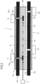
- Two electrical contacts 121a, 121b are provided, which extend through the carrier plate 13 to the active layer 161. More precisely, the contact 121a is connected to one of the sections 163 of the active layer 161 located outside the waveguide core 141, while the other contact 121b contacts the other section 164 of the active layer 161 located outside the waveguide core 141. Thus, the contacts 121a, 121b protrude as little as possible into a wave guided in the optical waveguide. This is shown in Fig. 5 which shows an optical wave OW guided in the waveguide 14.
- the contacts 121a, 121b each have a first section 1211a, 1211b extending perpendicular to the carrier plate 13, and a second section 1212a, 1212b, wherein the second section 1212a, 1212b each extends at an angle from the first section 1211a, 1211b and is connected to the associated section 163, 164 of the active layer 161.
- the first sections 1211a, 1211b each extend perpendicular to the second sections 1212a, 1212b.
- the contacting explained can also be used for other electro-optically active material layers; e.g. also for electro-optically active elements that comprise more than one active layer and/or that have one or more layers of a semiconductor material (e.g. in the form of an Fe-doped InGaAs layer) instead of a layer of a two-dimensional material (cf. e.g. the Fig. 7 to 11 ).
- a semiconductor material e.g. in the form of an Fe-doped InGaAs layer
- Figure 6 shows the Fig. 4 and 5 shown area of the circuit board 1 in plan view.
- Figure 7 shows analogous to Fig. 4 a section through a printed circuit board according to the invention in the region of an electro-optically active material layer 151, which is in particular part of a light modulator (e.g. corresponding to the first electro-optically active material layer 151 of the Figure 1 ).
- Contacting is carried out analogously to Figure 4 via electrical contacts 111a, 111b, namely via their second sections 1112a, 1112b, which each extend at an angle from first sections 1111a, 1111b.
- the electro-optically active material layer 151 is in the embodiment of the Fig. 7 Part of a PIN diode structure, wherein the active layer 151 is adjoined on one side by a p-doped layer 181 and on the other side by an n-doped layer 171.
- the layers 151, 181 and 171 are in particular III-V semiconductor layers; e.g. based on indium phosphide, wherein the active layer 151 consists of InGaAs and the doped layers 171, 181 consist of p- and n-doped indium phosphide, respectively.
- a modulated electrical voltage is applied to the active layer 151 via the p-layer 171 and the n-layer 181.
- the voltage changes the refractive index and the absorption of the active layer 151 and thus of the waveguide 14, whereby a light modulation can be generated depending on the applied voltage.
- Such an electro-optical element 15 can also be used as a light receiver operated by measuring the photovoltages and/or currents caused by light irradiation.
- the layers 151, 171, 181 each have a central section 152, 172, 182, which extends in the region of the waveguide core 141, as well as two lateral sections 153, 154, 173, 174, 183, 184 which run outside the waveguide core 141 in the cladding 142 of the waveguide 14.
- One (in Fig. 7 The (left) contact 111a is connected to the left lateral portion 173 of the p-doped layer 171, while the right contact 111b is connected to the right lateral portion 184 of the n-doped layer 181.
- FIG. 8 An alternative embodiment of the electro-optical element 15 for light modulation is shown in Fig. 8
- two electro-optically active layers 151a, 151b are provided, which run parallel to one another and are each formed from a two-dimensional material and which are electrically separated from one another by a dielectric layer 190 (e.g., made of silicon nitride or silicon oxide) running between them.
- the contacting of the electro-optical element 15 is carried out similarly to the Fig. 7 via a contacting of a left contact section 153a of the upper electro-optically active layer 151a with the left contact 111a and a contacting of a right contact section 153b of the lower electro-optically active layer 151b with the right contact 111b.
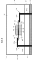
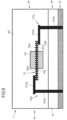
- FIGS 9 and 10 show further possible embodiments of an electro-optical element 15 of the circuit arrangement according to the invention, which can be used both for light modulation and for light detection.
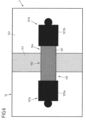
- the electro-optical element 15 of the Fig. 9 corresponds to that of the Fig. 8 , however, the active layers 151a, 151b are not formed to completely overlap each other. Rather, the lower contact layer 151b does not extend into the area of the left contact section 153a of the upper contact layer 151a, and the upper contact layer 151a does not extend into the area of the right contact section 153b of the lower contact layer 151b. Via such a contact, the electro-optical element 15 can be operated as a light modulator.
- the electro-optical element 15 of the Fig. 9 is in Fig. 11 shown in top view.
- a photoconductor detector By contacting both the upper and the lower active layers 151a, 151b, ie by connecting the active layers 151a, 151b in parallel, a photoconductor detector is realized; cf. Fig. 10 .
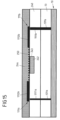
- the Figures 12 to 17 relate to steps in the production of a circuit arrangement according to the invention in the form of a printed circuit board using a variant of the inventive method. In each case, a section perpendicular to a carrier plate 13 is shown.
- the electro-optical component of the printed circuit board produced using this method can be used, in particular, as a photoconductor detector.
- a first polymer layer 240 is first formed on one side of the carrier plate 13 (e.g., by spin-coating the polymer material onto the carrier 13), which forms part of the cladding of an optical waveguide.
- an electrical layer 10 e.g., comprising at least one conductor track
- the electrical layer 10 is only created later or at least completed later.
- a recess 241 (e.g., with a width of 3 to 7 ⁇ m) is created (particularly by etching), which serves to form a section of the waveguide core.
- the recess 241 is created with a depth (e.g., 2 to 4 ⁇ m) that corresponds at least approximately to half the desired height of the waveguide core.
- the recess 241 is filled with a core polymer material 242 that has a higher refractive index than the polymer material of the polymer layer 240.
- the core polymer material 242 is applied in a sufficient thickness to fill the recess 241, with excess material outside the recess 241 being removed again.
- a layer 250 of an electro-optically active material is produced on the polymer layer 240 and the core polymer material 242 ( Fig. 13 ); e.g., consisting of a III-V semiconductor material or a two-dimensional material.
- the layer 250 is initially located on a carrier 251 (e.g., a carrier foil made of metal), which is removed after the layer 250 has been arranged on the polymer layer 240 (ELO method, as already mentioned above).
- ELO method as already mentioned above.
- the preparation of the active Layer(s) are described separately below for two-dimensional material and for III-V semiconductor layers.
- the thin active layer 250 holds without further bonding, particularly due to van der Waals forces.
- transferring smaller active segments may also be useful. For example, electro-optical conversion can be concentrated on selected areas of the circuit board 1. It is also conceivable that different active layers (layer segments) are arranged for different component functions.
- the carrier 251 is completely removed, and the active material layer 250 is removed wherever it is not needed.
- the material of the active layer 250 should essentially remain only at the desired locations for electro-optical conversion, but should protrude laterally from the waveguide core for contacting, for example.
- through-openings (vias) 131a, 131b are now created in the carrier 13 and in the polymer layer 240 by further lithography and at least one etching step.
- first contact sections 1111a, 1111b are arranged (created), which extend from a top side of the polymer layer 240 facing the active layer 250 through the through-openings 131a, 131b to the electrical plane 10 (i.e., to a side of the carrier 13 facing away from the polymer layer 240).
- the through-openings 131a, 131b are filled with a conductive material (e.g., solder) to produce the first contact sections 1111a, 1111b.
- the production of the through-openings 131a, 131b and the first contact sections 1111a, 1111b takes place before the arrangement of the active layer 250. It is also possible that the sections of the through-openings 131a, 131b in the carrier 13 and also the partial section of the first contact sections 1111a, 1111b extending there are already present at the beginning of the printed circuit board production (in particular before the production of the polymer layer 240). The arrangement of at least one electronic circuit on the carrier 13 takes place in particular after the production of at least the contact sections 1111a, 1111b.
- Second contact sections 1112a, 1112b are then created on the top side of the polymer layer 240 (e.g. by vapor deposition of gold or another metal and structuring), which are each connected on the one hand to the first contact sections 1111a, 1111b and on the other hand to the active layer 250.
- the first and second contact sections 1111a, 1111b, 1112a, 1112b together form the contacts 111a, 111b.
- a further polymer layer 244 of core polymer material is produced, which at least partially covers the polymer layer 240, the second contact sections 1112a, 1112b and/or the active layer 250 ( Fig. 15 ) and which serves to create an upper section of the waveguide core.
- the polymer layer 244 fills any existing trenches and can be planarized after its creation. It is conceivable that the polymer layer 244 is created with a thickness corresponding to half the desired height of the waveguide core.
- the polymer layer 244 is structured according to the desired course of the optical waveguide (following the course of the recess 243) in order to form the complete waveguide core 141 ( Fig. 16 ).
- a further polymer layer 245 is applied and cured, which forms an upper cladding layer of the optical waveguide, as in Fig. 17 shown.
- the polymer layer 245 can be formed from the same polymer material as the lower polymer layer 240.
- the optical layer is thus completed.
- the electrical layer can now be populated and/or the optical layer can be connected or pressed to another carrier in a sandwich structure.
- Fig. 18 relates to a modification of the manufacturing process, according to which the waveguide core 141 is produced in one step.
- a core material layer in particular similar to the polymer layer 244 of the Fig. 15 ) and structured accordingly (in particular, etched).
- the waveguide core 141 produced in this way borders the active layer 250, i.e., the active layer 250 does not extend through the waveguide core in this variant.
- the waveguide core 241 is produced not in the upper cladding layer 245, but in the lower cladding layer 240.
- a modification of the method of Fig. 12 to 17 after generating the right contact 111b a first, lower electro-optically active layer 250a and then a dielectric layer 251 is produced ( Fig. 19 and 20 ).
- dielectric layer 251 for example, a silicon nitride layer (approximately with a thickness of a few 10 nm, e.g. 35 nm) is produced (e.g. sputtered on).
- the lower electro-optically active layer 250a is in contact with the upper portion 1112b (e.g., in the form of a gold contact) of the contact 111b.
- the upper portion 1112b e.g., in the form of a gold contact
- a portion of the left contact 111a is also fabricated, namely its first portion 1111a penetrating the through-opening 131a and a portion 1113a of the upper portion 1111a.
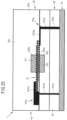
- a second, upper electro-optically active layer 250b is produced, which is arranged at least in sections on the dielectric layer 251 ( Fig. 21 ).
- the electro-optically active layers 250a, 250b each consist, in particular, of a two-dimensional material (e.g., graphene), wherein more than two of these layers may be provided.
- a further part 1114a of the contact 111a is produced to complete the upper contact section 1112a of the contact 111a ( Fig. 22 ).
- the part 1114a of the contact 111a contacts a portion of the upper active layer 250b, so that an electro-optically active element similar to that of the Fig. 9
- the upper polymer cladding layer 245 is produced as shown in Fig. 23 shown.
- the electro-optically active element is not constructed from layers of a two-dimensional material, but from semiconductor layers, e.g. similar to the electro-optical element of the Fig. 7
- the production of the printed circuit board or the corresponding printed circuit board section is carried out analogously to the Fig. 19 to 22
- the finished structure is in Fig. 24 shown, according to which the partial section 1114a of the contact 111a is separated by an insulation 1115 (e.g. made of silicon nitride or silicon oxide), in particular from the active layer 151.
- an insulation 1115 e.g. made of silicon nitride or silicon oxide
- lattice-matched InGaAs layers on an InP substrate can be used. Such layers are grown, for example, by metal-organic chemical vapor deposition (MOCVD) on an InP substrate.
- MOCVD metal-organic chemical vapor deposition
- a thin sacrificial layer made of a selectively easily etched material e.g., AlAs
- a thin layer e.g., with a thickness between 100 nm and 200 nm
- the active material e.g., InGaAs
- Doping is also possible to achieve the desired component function.
- iron atoms can be incorporated as recombination centers.
- a sequence of undoped Zn doping and S doping can be used, for example.
- the doping can also be applied to the InP edge layers (InP:n/InGaAs/InP:p heterostructure).
- the (particularly flexible) carrier 251 (see Fig. 13 ) is evaporated; for example, in the form of a metal layer (e.g., a gold layer).
- the epitaxial substrate is immersed in an etching solution selective for the sacrificial layer, thus separating the semiconductor layer and the carrier from the (thick) epitaxial substrate.
- the upper contact section (cf. contact 1112a in Fig. 24 ) must be connected without short circuit to the lower contact section (section 1111a in Fig. 24 ), which is why the dielectric layer 1115 is provided as an insulator. Openings can be opened in layer 1115 and windows can be opened above the lateral sections (contact areas) of the active layer, which are then suitably connected to one another by gold vapor deposition and patterning. It can be advantageous if the same active layer is used for a modulator and a detector, i.e., only one ELO and transfer process is required. Thus, an electroabsorption modulator can also be used inversely as a detector by applying a voltage in the reverse direction; the photocurrent follows the optical modulation at high speed.
- a modulator comprising active material layers formed from a two-dimensional material can also have the active layers connected in parallel to create a photoconductor detector. It is particularly conceivable to use the same active layers to create both a light absorption modulator and a light detector. For example, in this case, the light detector is adjacent to the light absorption modulator.
- Fig. 25 shows a further embodiment of the circuit arrangement according to the invention, again in the form of a printed circuit board, wherein two optical waveguides 14a, 14b are provided to establish an optical communication connection between two ICs 11, 12.
- Electro-optically active material layers 151', 151" (modulators or components of modulators) and 161', 161" (detectors or components of detectors) are integrated into the optical waveguides 14a, 14b, wherein the electro-optically active material layers 151', 151", 161', 161" are arranged adjacent to a core 141a, 141b of the respective waveguide 14a, 14b or extend at least partially within the core 141a, 141b.
Landscapes
- Physics & Mathematics (AREA)
- General Physics & Mathematics (AREA)
- Optics & Photonics (AREA)
- Nonlinear Science (AREA)
- Engineering & Computer Science (AREA)
- Microelectronics & Electronic Packaging (AREA)
- Optical Integrated Circuits (AREA)
Claims (14)
- Ensemble circuit de commutation, comprenant- au moins un premier et un deuxième circuit électronique (11, 12) ;- au moins un guide d'onde optique (14, 14a, 14b), le noyau (141, 141a, 141b) et la gaine (142) du guide d'onde optique (14, 14a, 14b) étant formés d'un matériau amorphe ;- au moins un support (13) sur lequel est agencé le au moins un guide d'onde optique (14, 14a, 14b) ; et- au moins une première couche de matériau électro-optiquement actif (151, 151', 151", 151a, 151b) connectée électriquement au premier circuit électronique (11) et conçue pour convertir un signal électrique reçu du premier circuit électronique (11) par l'intermédiaire d'un premier contact électrique (111a, 111b) en un signal optique se propageant dans le au moins un guide d'onde optique (14, 14a, 14b), et au moins une deuxième couche de matériau électro-optiquement actif (161, 161', 161") connectée électriquement au deuxième circuit électronique (12), qui est conçue pour convertir un signal optique généré par la première couche de matériau électro-optiquement actif (151, 151', 151", 151a, 151b) et se propageant dans le au moins un guide d'onde optique (14, 14a, 14b) en un signal électrique pouvant être conduit au deuxième circuit électronique (12) par l'intermédiaire d'un deuxième contact électrique (121a, 121b), dans lequel- les connexions électriques entre les circuits électroniques (11, 12) et les couches de matériau électro-optiquement actif (151, 151', 151", 151a, 151b, 161, 161', 161") sont établies en ce que les contacts électriques (111a, 111b, 121a, 121b) s'étendent respectivement depuis les circuits électroniques (11, 12) à travers au moins une partie de la gaine (142) du au moins un guide d'onde optique (14, 14a, 14b) à travers les couches de matériau électro-optiquement actif (151, 151', 151", 151a, 151b, 161, 161', 161") ou sont connectées à une partie des couches de matériau électro-optiquement actif (151, 151', 151", 151a, 151b, 161, 161', 161") qui dépasse de la gaine (142) du au moins un guide d'onde optique (14, 14a, 14b), et- les circuits électroniques (11, 12) sont agencés sur le au moins un support (13), et dans lequel- les circuits électroniques (11, 12) sont agencés sur un côté du support (13) et le au moins un guide d'onde optique (14, 14a, 14b) est agencé sur l'autre côté du au moins un support (13), dans lequel- les couches de matériau électro-optiquement actif (151, 151', 151", 151a, 151b, 161, 161', 161") s'étendent au moins partiellement dans le au moins un guide d'onde optique (14, 14a, 14b),caractérisé en ce que
les couches de matériau électro-optiquement actif (151, 151', 151", 151a, 151b, 161, 161', 161") s'étendent au moins partiellement dans le noyau (141, 141a, 141b) du au moins un guide d'onde optique (14, 14a, 14b) ou s'étendent de manière adjacente sur le côté du noyau (141, 141a, 141b) du au moins un guide d'onde optique (14, 14a, 14b) faisant face au support (13). - Ensemble circuit de commutation selon la revendication 1, caractérisé en ce que l'ensemble circuit de commutation est un circuit imprimé (1) ou une micropuce.
- Ensemble circuit de commutation selon l'une quelconque des revendications précédentes, caractérisé en ce que la gaine (142) et/ou le noyau (141, 141a, 141b) de l'au moins un guide d'onde optique (14, 14a, 14b) sont formés d'un matériau électriquement isolant.
- Ensemble circuit de commutation selon l'une quelconque des revendications précédentes, caractérisé en ce que le au moins un guide d'onde optique (14, 14a, 14b) est formé au moins partiellement d'un matériau généré à partir de la phase liquide ou de la phase gazeuse sur le support (13) et/ou est formé au moins partiellement d'un matériau polymère, de dioxyde de silicium et/ou de nitrure de silicium.
- Ensemble circuit de commutation selon l'une quelconque des revendications précédentes, caractérisé en ce que les contacts électriques (111a, 111b, 121a, 121b) s'étendent en particulier à travers une ouverture de passage (131a, 131b, 132a, 132b) dans le support (13).
- Ensemble circuit de commutation selon l'une quelconque des revendications précédentes, caractérisé en ce que le au moins un guide d'onde optique (14, 14a, 14b) s'étend entre deux supports (13, 130).
- Ensemble circuit de commutation selon l'une quelconque des revendications précédentes, caractérisé en ce que les couches de matériau électro-optiquement actif (151, 151', 151", 151a, 151b, 161, 161', 161") sont formées d'un matériau différent de celui du au moins un guide d'onde optique (14, 14a, 14b), et/ou en ce que les couches de matériau électro-optiquement actif (151, 151', 151", 151a, 151b, 161, 161', 161") sont formées d'un matériau cristallin.
- Ensemble circuit de commutation selon l'une quelconque des revendications précédentes, caractérisé en ce que les couches de matériau électro-optiquement actif (151, 151', 151", 151a, 151b, 161, 161', 161") comprennent un matériau bidimensionnel ou un matériau semi-conducteur ou sont formées d'un tel matériau.
- Ensemble circuit de commutation selon la revendication 8, caractérisé en ce que le matériau bidimensionnel est formé de graphène, de nitrure de carbone graphitique à base de triazine, de germanène, de disulfure de molybdène, de diséléniure de molybdène, de silice et/ou de phosphore noir, ou comprend au moins un de ces matériaux.
- Ensemble circuit de commutation selon la revendication 8, caractérisé en ce que le matériau semi-conducteur est un matériau semi-conducteur III-V.
- Ensemble circuit de commutation selon l'une quelconque des revendications précédentes, caractérisé en ce que le noyau (141, 141a, 141b) du au moins un guide d'onde optique (14, 14a, 14b) a une section transversale d'au moins 1 µm2 ou d'au moins 5 µm2 et/ou les couches de matériau électro-optiquement actif (151, 151a, 151b, 161) ont une épaisseur d'au plus 500 nm ou d'au plus 200 nm ou d'au plus 50 nm.
- Ensemble circuit de commutation selon l'une quelconque des revendications précédentes, caractérisé en ce que la première couche de matériau électro-optiquement actif (151, 151', 151", 151a, 151b) ou une structure multicouche comprenant la première couche de matériau électro-optiquement actif forme un modulateur pour moduler une onde optique guidée dans le au moins un guide d'onde optique (14, 14a, 14b), qui est générée par une source de lumière externe (17) séparée dudit au moins un guide d'onde optique (14, 14a, 14b), ou fait partie d'un tel modulateur, et/ou la deuxième couche de matériau électro-optiquement actif (161, 161', 161") forme un détecteur de lumière ou fait partie d'un détecteur de lumière.
- Procédé de fabrication d'un ensemble circuit de commutation selon l'une quelconque des revendications précédentes, comportant les étapes suivantes :- fournir un support (13) ;- agencer sur le support (13) une couche de matériau amorphe (240) formant une partie d'une gaine d'un guide d'onde optique (14) ;- agencer au moins une couche électro-optiquement active (250) sur la couche de matériau (240) ;- produire un contact électrique (111a, 111b) qui s'étend au moins partiellement à travers la couche de matériau amorphe (240) ou au-delà de la couche de matériau amorphe (240) jusqu'à la couche électro-optiquement active (250),caractérisé en ce queun évidement (243) est produit dans la couche de matériau amorphe (240) et l'évidement (243) est rempli d'un matériau de noyau (242) avant d'agencer la couche électro-optiquement active (250) pour produire une première partie d'un noyau (141) du guide d'onde optique (14), la couche électro-optiquement active (250) étant agencée sur la couche de matériau amorphe (240) de manière à s'étendre au-delà du matériau de noyau (242),sur un côté de la couche électro-optiquement active (250) opposé à la première partie du noyau (141) du guide d'onde optique (14), une deuxième partie du noyau (141) du guide d'onde optique (14) est produite, etaprès avoir produit les première et deuxième parties du noyau (14) du guide d'onde optique (14), une autre couche de matériau (245) est produite, qui forme une autre partie de la gaine du guide d'onde optique (14).
- Procédé selon la revendication 13, caractérisé en ce que la au moins une couche électro-optiquement active (250) se trouve, avant d'être agencée sur la couche de matériau amorphe (240), sur un matériau de support différent du support (13), qui est enlevé après que la couche électro-optiquement active (250) a été agencée sur la couche de matériau amorphe (240), la au moins une couche électro-optiquement active (250) étant structurée en particulier après l'enlèvement du matériau de support.
Applications Claiming Priority (2)
| Application Number | Priority Date | Filing Date | Title |
|---|---|---|---|
| DE102016202765.4A DE102016202765A1 (de) | 2016-02-23 | 2016-02-23 | Schaltkreisanordnung und Verfahren zum Herstellen einer Schaltkreisanordnung |
| PCT/EP2017/053930 WO2017144462A1 (fr) | 2016-02-23 | 2017-02-21 | Ensemble circuit de commutation et procédé de fabrication d'un ensemble circuit de commutation |
Publications (2)
| Publication Number | Publication Date |
|---|---|
| EP3420390A1 EP3420390A1 (fr) | 2019-01-02 |
| EP3420390B1 true EP3420390B1 (fr) | 2025-04-02 |
Family
ID=58266558
Family Applications (1)
| Application Number | Title | Priority Date | Filing Date |
|---|---|---|---|
| EP17710139.1A Active EP3420390B1 (fr) | 2016-02-23 | 2017-02-21 | Ensemble circuit de commutation et procédé de fabrication d'un ensemble circuit de commutation |
Country Status (4)
| Country | Link |
|---|---|
| US (1) | US10436980B2 (fr) |
| EP (1) | EP3420390B1 (fr) |
| DE (1) | DE102016202765A1 (fr) |
| WO (1) | WO2017144462A1 (fr) |
Families Citing this family (4)
| Publication number | Priority date | Publication date | Assignee | Title |
|---|---|---|---|---|
| US10802375B2 (en) * | 2017-09-15 | 2020-10-13 | Samsung Electronics Co., Ltd. | Optically-controlled switch |
| US10754093B2 (en) * | 2018-05-15 | 2020-08-25 | Lightwave Logic Inc. | Fabrication process of polymer based photonic apparatus and the apparatus |
| CN112750847B (zh) * | 2019-10-31 | 2024-10-18 | 台湾积体电路制造股份有限公司 | 半导体装置及其形成方法 |
| TWI803954B (zh) * | 2021-08-27 | 2023-06-01 | 國立清華大學 | 太赫茲光調制器及太赫茲空間光調制器 |
Citations (1)
| Publication number | Priority date | Publication date | Assignee | Title |
|---|---|---|---|---|
| US20080044127A1 (en) * | 2003-12-29 | 2008-02-21 | At & S Austria Technologie & Systemtechnik Aktiengesellschaft | Printed Circuit Board Element Comprising at Least One Optical Waveguide, and Method for the Production of Such a Printed Circuit Board Element |
Family Cites Families (17)
| Publication number | Priority date | Publication date | Assignee | Title |
|---|---|---|---|---|
| US6690845B1 (en) * | 1998-10-09 | 2004-02-10 | Fujitsu Limited | Three-dimensional opto-electronic modules with electrical and optical interconnections and methods for making |
| US6611635B1 (en) * | 1998-10-09 | 2003-08-26 | Fujitsu Limited | Opto-electronic substrates with electrical and optical interconnections and methods for making |
| DE10027767A1 (de) * | 2000-06-07 | 2001-12-13 | Fischer Artur Werke Gmbh | Behältnis zum Ausbringen von Nützlingen |
| US6694069B2 (en) * | 2000-10-30 | 2004-02-17 | Kyocera Corporation | Optical integrated circuit substrate and optical module |
| JP4297379B2 (ja) * | 2007-02-02 | 2009-07-15 | ボッシュ株式会社 | Noxセンサの故障診断装置及び故障診断方法 |
| JP2009025726A (ja) | 2007-07-23 | 2009-02-05 | Nitto Denko Corp | 光導波路デバイスおよびその製造方法 |
| KR20100133767A (ko) * | 2009-06-12 | 2010-12-22 | 삼성전기주식회사 | 광도파로용 인쇄회로기판 및 그 제조방법 |
| US8951968B2 (en) * | 2009-10-05 | 2015-02-10 | Northwestern University | Methods of treating depression and other related diseases |
| US9217830B2 (en) * | 2010-05-14 | 2015-12-22 | Cornell University | Electro-optic modulator structures, related methods and applications |
| US9477350B2 (en) * | 2011-04-26 | 2016-10-25 | Sentons Inc. | Method and apparatus for active ultrasonic touch devices |
| US9117221B2 (en) * | 2011-06-30 | 2015-08-25 | Flite, Inc. | System and method for the transmission of live updates of embeddable units |
| KR20130031598A (ko) * | 2011-09-21 | 2013-03-29 | 한국전자통신연구원 | 광 도파로 |
| EP2629352A1 (fr) * | 2012-02-17 | 2013-08-21 | Oxis Energy Limited | Électrode de feuille métallique renforcée |
| US8909002B2 (en) | 2012-04-05 | 2014-12-09 | Panasonic Corporation | Light modulator, optical pickup, and light modulation module |
| CN105264430B (zh) * | 2013-12-05 | 2019-05-28 | 华为技术有限公司 | 一种光调制器及平面光子器件模组 |
| GB2525427A (en) * | 2014-04-24 | 2015-10-28 | Ibm | Waveguide structure |
| JP6460516B2 (ja) * | 2014-10-28 | 2019-01-30 | 日東電工株式会社 | 光電気混載基板 |
-
2016
- 2016-02-23 DE DE102016202765.4A patent/DE102016202765A1/de active Pending
-
2017
- 2017-02-21 US US16/079,206 patent/US10436980B2/en active Active
- 2017-02-21 EP EP17710139.1A patent/EP3420390B1/fr active Active
- 2017-02-21 WO PCT/EP2017/053930 patent/WO2017144462A1/fr not_active Ceased
Patent Citations (1)
| Publication number | Priority date | Publication date | Assignee | Title |
|---|---|---|---|---|
| US20080044127A1 (en) * | 2003-12-29 | 2008-02-21 | At & S Austria Technologie & Systemtechnik Aktiengesellschaft | Printed Circuit Board Element Comprising at Least One Optical Waveguide, and Method for the Production of Such a Printed Circuit Board Element |
Also Published As
| Publication number | Publication date |
|---|---|
| DE102016202765A1 (de) | 2017-08-24 |
| US10436980B2 (en) | 2019-10-08 |
| EP3420390A1 (fr) | 2019-01-02 |
| US20190094461A1 (en) | 2019-03-28 |
| WO2017144462A1 (fr) | 2017-08-31 |
Similar Documents
| Publication | Publication Date | Title |
|---|---|---|
| DE69125888T2 (de) | Verfahren zur Lichtmodulation und optischer Modulator | |
| EP0193852B1 (fr) | Matrice à résonateurs intégrés pour la séparation/liaison à longueur d'onde sélective des voies dans le champ de la fréquence de communication optique | |
| DE69223463T2 (de) | Optische Halbleiter-Wellenleitervorrichtung und ihr Herstellungsverfahren | |
| EP0849847B1 (fr) | Elément optoélectronique avec une structure MQW | |
| EP3420390B1 (fr) | Ensemble circuit de commutation et procédé de fabrication d'un ensemble circuit de commutation | |
| DE102011005422B4 (de) | Elektrooptischer Modulator | |
| DE69429406T2 (de) | Verfahren zum Herstellen einer monolitisch integrierten Struktur mit optoelektronischen Komponenten und so hergestellte Strukturen | |
| DE60219815T2 (de) | Monolitische elektronische mehrlagenanordnung und deren herstellungsverfahren | |
| DE102015219056B4 (de) | Halbleiterlichtquelle und Verfahren zur Herstellung einer Halbleiterlichtquelle | |
| DE3300986A1 (de) | Mehrschichtige optische integrierte schaltung | |
| DE69123215T2 (de) | Optisches Signalverteilungsnetzwerk | |
| WO1998011461A1 (fr) | Systeme pour interconnecter des guides d'ondes | |
| DE69734559T2 (de) | Optischer Koppler | |
| DE10201126A1 (de) | Optoelektronisches Bauelement und Verfahren zu seiner Herstellung | |
| EP0053742A1 (fr) | Procédé de transmission de signaux, dispositif semiconducteur et dispositif électro-optique pour la réalisation de ce procédé | |
| DE60215131T2 (de) | Integriertes Halbleiterlaser-Wellenleiter-Element | |
| EP3198750B1 (fr) | Modulateur d'injection | |
| DE19652533C1 (de) | Optoelektronischer Modul | |
| DE10201124A1 (de) | Optoelektronisches Bauelement und Verfahren zu seiner Herstellung | |
| DE102016224615B4 (de) | Modulatoranordnung und Verfahren zum Modulieren von Licht | |
| EP0328886A2 (fr) | Isolateur pour l'isolation optique des composants intégrés | |
| DE60109045T2 (de) | Integrierte optische Weglenkungs- und Wellenlängenkonversionsmatrix | |
| DE602005004945T2 (de) | Herstellung einer optischen Verbindungsschicht auf einem elektronischen Schaltkreis | |
| EP3577506A1 (fr) | Circuit électro-optique avec une voie de transmission optique, assemblage électro-optique pour le montage dans un tel circuit électro-optique et procédé pour la génération d'une interface optique d'un circuit électro-optique | |
| DE102016216811A1 (de) | Optokoppler mit einer optischen Übertragungsstrecke und elektrischen Anschlüssen und elektronische Baugruppe, in der ein solcher Optokoppler eingebaut ist |
Legal Events
| Date | Code | Title | Description |
|---|---|---|---|
| STAA | Information on the status of an ep patent application or granted ep patent |
Free format text: STATUS: UNKNOWN |
|
| STAA | Information on the status of an ep patent application or granted ep patent |
Free format text: STATUS: THE INTERNATIONAL PUBLICATION HAS BEEN MADE |
|
| PUAI | Public reference made under article 153(3) epc to a published international application that has entered the european phase |
Free format text: ORIGINAL CODE: 0009012 |
|
| STAA | Information on the status of an ep patent application or granted ep patent |
Free format text: STATUS: REQUEST FOR EXAMINATION WAS MADE |
|
| 17P | Request for examination filed |
Effective date: 20180918 |
|
| AK | Designated contracting states |
Kind code of ref document: A1 Designated state(s): AL AT BE BG CH CY CZ DE DK EE ES FI FR GB GR HR HU IE IS IT LI LT LU LV MC MK MT NL NO PL PT RO RS SE SI SK SM TR |
|
| AX | Request for extension of the european patent |
Extension state: BA ME |
|
| RIN1 | Information on inventor provided before grant (corrected) |
Inventor name: KLEINERT, MORITZ Inventor name: SCHELL, MARTIN |
|
| DAV | Request for validation of the european patent (deleted) | ||
| DAX | Request for extension of the european patent (deleted) | ||
| STAA | Information on the status of an ep patent application or granted ep patent |
Free format text: STATUS: EXAMINATION IS IN PROGRESS |
|
| 17Q | First examination report despatched |
Effective date: 20200317 |
|
| RAP3 | Party data changed (applicant data changed or rights of an application transferred) |
Owner name: FRAUNHOFER-GESELLSCHAFT ZUR FOERDERUNG DER ANGEWANDTEN FORSCHUNG E.V. |
|
| GRAP | Despatch of communication of intention to grant a patent |
Free format text: ORIGINAL CODE: EPIDOSNIGR1 |
|
| STAA | Information on the status of an ep patent application or granted ep patent |
Free format text: STATUS: GRANT OF PATENT IS INTENDED |
|
| INTG | Intention to grant announced |
Effective date: 20241028 |
|
| GRAS | Grant fee paid |
Free format text: ORIGINAL CODE: EPIDOSNIGR3 |
|
| GRAA | (expected) grant |
Free format text: ORIGINAL CODE: 0009210 |
|
| STAA | Information on the status of an ep patent application or granted ep patent |
Free format text: STATUS: THE PATENT HAS BEEN GRANTED |
|
| AK | Designated contracting states |
Kind code of ref document: B1 Designated state(s): AL AT BE BG CH CY CZ DE DK EE ES FI FR GB GR HR HU IE IS IT LI LT LU LV MC MK MT NL NO PL PT RO RS SE SI SK SM TR |
|
| REG | Reference to a national code |
Ref country code: GB Ref legal event code: FG4D Free format text: NOT ENGLISH |
|
| REG | Reference to a national code |
Ref country code: CH Ref legal event code: EP |
|
| REG | Reference to a national code |
Ref country code: IE Ref legal event code: FG4D Free format text: LANGUAGE OF EP DOCUMENT: GERMAN |
|
| REG | Reference to a national code |
Ref country code: DE Ref legal event code: R096 Ref document number: 502017016776 Country of ref document: DE |
|
| REG | Reference to a national code |
Ref country code: NL Ref legal event code: MP Effective date: 20250402 |
|
| PG25 | Lapsed in a contracting state [announced via postgrant information from national office to epo] |
Ref country code: NL Free format text: LAPSE BECAUSE OF FAILURE TO SUBMIT A TRANSLATION OF THE DESCRIPTION OR TO PAY THE FEE WITHIN THE PRESCRIBED TIME-LIMIT Effective date: 20250402 |
|
| PG25 | Lapsed in a contracting state [announced via postgrant information from national office to epo] |
Ref country code: ES Free format text: LAPSE BECAUSE OF FAILURE TO SUBMIT A TRANSLATION OF THE DESCRIPTION OR TO PAY THE FEE WITHIN THE PRESCRIBED TIME-LIMIT Effective date: 20250402 Ref country code: FI Free format text: LAPSE BECAUSE OF FAILURE TO SUBMIT A TRANSLATION OF THE DESCRIPTION OR TO PAY THE FEE WITHIN THE PRESCRIBED TIME-LIMIT Effective date: 20250402 Ref country code: PT Free format text: LAPSE BECAUSE OF FAILURE TO SUBMIT A TRANSLATION OF THE DESCRIPTION OR TO PAY THE FEE WITHIN THE PRESCRIBED TIME-LIMIT Effective date: 20250804 |
|
| REG | Reference to a national code |
Ref country code: LT Ref legal event code: MG9D |
|
| PG25 | Lapsed in a contracting state [announced via postgrant information from national office to epo] |
Ref country code: NO Free format text: LAPSE BECAUSE OF FAILURE TO SUBMIT A TRANSLATION OF THE DESCRIPTION OR TO PAY THE FEE WITHIN THE PRESCRIBED TIME-LIMIT Effective date: 20250702 Ref country code: GR Free format text: LAPSE BECAUSE OF FAILURE TO SUBMIT A TRANSLATION OF THE DESCRIPTION OR TO PAY THE FEE WITHIN THE PRESCRIBED TIME-LIMIT Effective date: 20250703 |
|
| PG25 | Lapsed in a contracting state [announced via postgrant information from national office to epo] |
Ref country code: PL Free format text: LAPSE BECAUSE OF FAILURE TO SUBMIT A TRANSLATION OF THE DESCRIPTION OR TO PAY THE FEE WITHIN THE PRESCRIBED TIME-LIMIT Effective date: 20250402 |
|
| PG25 | Lapsed in a contracting state [announced via postgrant information from national office to epo] |
Ref country code: BG Free format text: LAPSE BECAUSE OF FAILURE TO SUBMIT A TRANSLATION OF THE DESCRIPTION OR TO PAY THE FEE WITHIN THE PRESCRIBED TIME-LIMIT Effective date: 20250402 |
|
| PG25 | Lapsed in a contracting state [announced via postgrant information from national office to epo] |
Ref country code: HR Free format text: LAPSE BECAUSE OF FAILURE TO SUBMIT A TRANSLATION OF THE DESCRIPTION OR TO PAY THE FEE WITHIN THE PRESCRIBED TIME-LIMIT Effective date: 20250402 |
|
| PG25 | Lapsed in a contracting state [announced via postgrant information from national office to epo] |
Ref country code: RS Free format text: LAPSE BECAUSE OF FAILURE TO SUBMIT A TRANSLATION OF THE DESCRIPTION OR TO PAY THE FEE WITHIN THE PRESCRIBED TIME-LIMIT Effective date: 20250702 |
|
| PG25 | Lapsed in a contracting state [announced via postgrant information from national office to epo] |
Ref country code: IS Free format text: LAPSE BECAUSE OF FAILURE TO SUBMIT A TRANSLATION OF THE DESCRIPTION OR TO PAY THE FEE WITHIN THE PRESCRIBED TIME-LIMIT Effective date: 20250802 |
|
| PG25 | Lapsed in a contracting state [announced via postgrant information from national office to epo] |
Ref country code: LV Free format text: LAPSE BECAUSE OF FAILURE TO SUBMIT A TRANSLATION OF THE DESCRIPTION OR TO PAY THE FEE WITHIN THE PRESCRIBED TIME-LIMIT Effective date: 20250402 |
|
| REG | Reference to a national code |
Ref country code: DE Ref legal event code: R097 Ref document number: 502017016776 Country of ref document: DE |
|
| PG25 | Lapsed in a contracting state [announced via postgrant information from national office to epo] |
Ref country code: SM Free format text: LAPSE BECAUSE OF FAILURE TO SUBMIT A TRANSLATION OF THE DESCRIPTION OR TO PAY THE FEE WITHIN THE PRESCRIBED TIME-LIMIT Effective date: 20250402 Ref country code: DK Free format text: LAPSE BECAUSE OF FAILURE TO SUBMIT A TRANSLATION OF THE DESCRIPTION OR TO PAY THE FEE WITHIN THE PRESCRIBED TIME-LIMIT Effective date: 20250402 |
|
| PG25 | Lapsed in a contracting state [announced via postgrant information from national office to epo] |
Ref country code: CZ Free format text: LAPSE BECAUSE OF FAILURE TO SUBMIT A TRANSLATION OF THE DESCRIPTION OR TO PAY THE FEE WITHIN THE PRESCRIBED TIME-LIMIT Effective date: 20250402 |
|
| PG25 | Lapsed in a contracting state [announced via postgrant information from national office to epo] |
Ref country code: EE Free format text: LAPSE BECAUSE OF FAILURE TO SUBMIT A TRANSLATION OF THE DESCRIPTION OR TO PAY THE FEE WITHIN THE PRESCRIBED TIME-LIMIT Effective date: 20250402 |
|
| PG25 | Lapsed in a contracting state [announced via postgrant information from national office to epo] |
Ref country code: SK Free format text: LAPSE BECAUSE OF FAILURE TO SUBMIT A TRANSLATION OF THE DESCRIPTION OR TO PAY THE FEE WITHIN THE PRESCRIBED TIME-LIMIT Effective date: 20250402 Ref country code: RO Free format text: LAPSE BECAUSE OF FAILURE TO SUBMIT A TRANSLATION OF THE DESCRIPTION OR TO PAY THE FEE WITHIN THE PRESCRIBED TIME-LIMIT Effective date: 20250402 |
|
| PG25 | Lapsed in a contracting state [announced via postgrant information from national office to epo] |
Ref country code: IT Free format text: LAPSE BECAUSE OF FAILURE TO SUBMIT A TRANSLATION OF THE DESCRIPTION OR TO PAY THE FEE WITHIN THE PRESCRIBED TIME-LIMIT Effective date: 20250402 |
|
| PLBE | No opposition filed within time limit |
Free format text: ORIGINAL CODE: 0009261 |
|
| STAA | Information on the status of an ep patent application or granted ep patent |
Free format text: STATUS: NO OPPOSITION FILED WITHIN TIME LIMIT |
|
| REG | Reference to a national code |
Ref country code: CH Ref legal event code: L10 Free format text: ST27 STATUS EVENT CODE: U-0-0-L10-L00 (AS PROVIDED BY THE NATIONAL OFFICE) Effective date: 20260211 |
|
| 26N | No opposition filed |
Effective date: 20260105 |
|
| PGFP | Annual fee paid to national office [announced via postgrant information from national office to epo] |
Ref country code: GB Payment date: 20260219 Year of fee payment: 10 |
|
| PGFP | Annual fee paid to national office [announced via postgrant information from national office to epo] |
Ref country code: DE Payment date: 20260225 Year of fee payment: 10 |
|
| PGFP | Annual fee paid to national office [announced via postgrant information from national office to epo] |
Ref country code: FR Payment date: 20260223 Year of fee payment: 10 |