EP3422546A1 - Circuit d'attaque de transistor - Google Patents
Circuit d'attaque de transistor Download PDFInfo
- Publication number
- EP3422546A1 EP3422546A1 EP17755827.7A EP17755827A EP3422546A1 EP 3422546 A1 EP3422546 A1 EP 3422546A1 EP 17755827 A EP17755827 A EP 17755827A EP 3422546 A1 EP3422546 A1 EP 3422546A1
- Authority
- EP
- European Patent Office
- Prior art keywords
- power supply
- voltage power
- circuit
- voltage
- low
- Prior art date
- Legal status (The legal status is an assumption and is not a legal conclusion. Google has not performed a legal analysis and makes no representation as to the accuracy of the status listed.)
- Granted
Links
Images


Classifications
-
- H—ELECTRICITY
- H03—ELECTRONIC CIRCUITRY
- H03K—PULSE TECHNIQUE
- H03K17/00—Electronic switching or gating, i.e. not by contact-making and –breaking
- H03K17/08—Modifications for protecting switching circuit against overcurrent or overvoltage
- H03K17/081—Modifications for protecting switching circuit against overcurrent or overvoltage without feedback from the output circuit to the control circuit
- H03K17/08104—Modifications for protecting switching circuit against overcurrent or overvoltage without feedback from the output circuit to the control circuit in field-effect transistor switches
-
- H—ELECTRICITY
- H02—GENERATION; CONVERSION OR DISTRIBUTION OF ELECTRIC POWER
- H02H—EMERGENCY PROTECTIVE CIRCUIT ARRANGEMENTS
- H02H9/00—Emergency protective circuit arrangements for limiting excess current or voltage without disconnection
- H02H9/04—Emergency protective circuit arrangements for limiting excess current or voltage without disconnection responsive to excess voltage
- H02H9/045—Emergency protective circuit arrangements for limiting excess current or voltage without disconnection responsive to excess voltage adapted to a particular application and not provided for elsewhere
-
- H—ELECTRICITY
- H02—GENERATION; CONVERSION OR DISTRIBUTION OF ELECTRIC POWER
- H02M—APPARATUS FOR CONVERSION BETWEEN AC AND AC, BETWEEN AC AND DC, OR BETWEEN DC AND DC, AND FOR USE WITH MAINS OR SIMILAR POWER SUPPLY SYSTEMS; CONVERSION OF DC OR AC INPUT POWER INTO SURGE OUTPUT POWER; CONTROL OR REGULATION THEREOF
- H02M1/00—Details of apparatus for conversion
- H02M1/08—Circuits specially adapted for the generation of control voltages for semiconductor devices incorporated in static converters
-
- H—ELECTRICITY
- H03—ELECTRONIC CIRCUITRY
- H03K—PULSE TECHNIQUE
- H03K17/00—Electronic switching or gating, i.e. not by contact-making and –breaking
- H03K17/08—Modifications for protecting switching circuit against overcurrent or overvoltage
- H03K17/081—Modifications for protecting switching circuit against overcurrent or overvoltage without feedback from the output circuit to the control circuit
- H03K17/0814—Modifications for protecting switching circuit against overcurrent or overvoltage without feedback from the output circuit to the control circuit by measures taken in the output circuit
- H03K17/08142—Modifications for protecting switching circuit against overcurrent or overvoltage without feedback from the output circuit to the control circuit by measures taken in the output circuit in field-effect transistor switches
-
- H—ELECTRICITY
- H03—ELECTRONIC CIRCUITRY
- H03K—PULSE TECHNIQUE
- H03K17/00—Electronic switching or gating, i.e. not by contact-making and –breaking
- H03K17/08—Modifications for protecting switching circuit against overcurrent or overvoltage
- H03K17/082—Modifications for protecting switching circuit against overcurrent or overvoltage by feedback from the output to the control circuit
- H03K17/0822—Modifications for protecting switching circuit against overcurrent or overvoltage by feedback from the output to the control circuit in field-effect transistor switches
-
- H—ELECTRICITY
- H03—ELECTRONIC CIRCUITRY
- H03K—PULSE TECHNIQUE
- H03K17/00—Electronic switching or gating, i.e. not by contact-making and –breaking
- H03K17/16—Modifications for eliminating interference voltages or currents
- H03K17/161—Modifications for eliminating interference voltages or currents in field-effect transistor switches
- H03K17/162—Modifications for eliminating interference voltages or currents in field-effect transistor switches without feedback from the output circuit to the control circuit
- H03K17/163—Soft switching
-
- H—ELECTRICITY
- H03—ELECTRONIC CIRCUITRY
- H03K—PULSE TECHNIQUE
- H03K17/00—Electronic switching or gating, i.e. not by contact-making and –breaking
- H03K17/16—Modifications for eliminating interference voltages or currents
- H03K17/161—Modifications for eliminating interference voltages or currents in field-effect transistor switches
- H03K17/165—Modifications for eliminating interference voltages or currents in field-effect transistor switches by feedback from the output circuit to the control circuit
- H03K17/166—Soft switching
-
- H—ELECTRICITY
- H03—ELECTRONIC CIRCUITRY
- H03K—PULSE TECHNIQUE
- H03K19/00—Logic circuits, i.e. having at least two inputs acting on one output; Inverting circuits
- H03K19/0175—Coupling arrangements; Interface arrangements
- H03K19/0185—Coupling arrangements; Interface arrangements using field effect transistors only
-
- H—ELECTRICITY
- H10—SEMICONDUCTOR DEVICES; ELECTRIC SOLID-STATE DEVICES NOT OTHERWISE PROVIDED FOR
- H10D—INORGANIC ELECTRIC SEMICONDUCTOR DEVICES
- H10D89/00—Aspects of integrated devices not covered by groups H10D84/00 - H10D88/00
- H10D89/60—Integrated devices comprising arrangements for electrical or thermal protection, e.g. protection circuits against electrostatic discharge [ESD]
- H10D89/601—Integrated devices comprising arrangements for electrical or thermal protection, e.g. protection circuits against electrostatic discharge [ESD] for devices having insulated gate electrodes, e.g. for IGFETs or IGBTs
-
- H—ELECTRICITY
- H10—SEMICONDUCTOR DEVICES; ELECTRIC SOLID-STATE DEVICES NOT OTHERWISE PROVIDED FOR
- H10D—INORGANIC ELECTRIC SEMICONDUCTOR DEVICES
- H10D89/00—Aspects of integrated devices not covered by groups H10D84/00 - H10D88/00
- H10D89/60—Integrated devices comprising arrangements for electrical or thermal protection, e.g. protection circuits against electrostatic discharge [ESD]
- H10D89/601—Integrated devices comprising arrangements for electrical or thermal protection, e.g. protection circuits against electrostatic discharge [ESD] for devices having insulated gate electrodes, e.g. for IGFETs or IGBTs
- H10D89/611—Integrated devices comprising arrangements for electrical or thermal protection, e.g. protection circuits against electrostatic discharge [ESD] for devices having insulated gate electrodes, e.g. for IGFETs or IGBTs using diodes as protective elements
Definitions
- This application relates to the field of drive circuit technologies, and in particular, to a drive circuit of a transistor.
- a high-voltage transistor drive chip is mainly used to drive a power device such as a MOSFET (Metal-Oxide-Semiconductor Field-Effect Transistor) or an IGBT (Insulated Gate Bipolar Transistor), and is generally applied to fields such as industries and household appliance inverters.
- a power device such as a MOSFET (Metal-Oxide-Semiconductor Field-Effect Transistor) or an IGBT (Insulated Gate Bipolar Transistor)
- the high-voltage transistor drive chip has a high-voltage power supply domain and a low-voltage power supply domain, static electricity between the power supply domains needs to be discharged by using a high-voltage device.
- an ESD Electrostatic Discharge
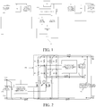
- the chip includes two power supply domains: a low-voltage power supply domain (VCC is a low-voltage power supply and VSS is a low-voltage ground) and a high-voltage power supply domain (VB is a high-voltage power supply and VS is a high-voltage ground).
- the two power supply domains are connected together by using a level-shifter circuit (level shifter, and inside of FIG. 7 includes a level-shifter 1 and a level-shifter 2 that are independent and in a same structure) and a high-voltage ESD device.
- a level-shifter circuit level shifter, and inside of FIG. 7 includes a level-shifter 1 and a level-shifter 2 that are independent and in a same structure
- a high-voltage ESD device Inside of an independent power supply domain, and power supply grounded VB-VS and VCC-VSS include independent ESD devices (which are commonly a diode, a triode, a CMOS tube, and the like), used to perform
- the level-shifter mainly includes: a DMOS (M1 and M2 in FIG. 7 ), a DMOS source device (a source is grounded in FIG. 7 ), and a DMOS drain detection circuit (formed by detection resistors R1 and R2 and voltage stabilizing tubes Z1 and Z2 in FIG. 7 ). Voltages on the detection resistors R1 and R2 are changed by controlling on and off of the DMOS-M1 and the DMOS-M2, to shift a low-voltage signal to a high-voltage signal.
- This application is aimed to at least resolve one of the technical problems in the related technology to some extent.
- the objective of this application is to provide a drive circuit of a transistor.
- the drive circuit of the transistor has an advantage of a strong anti-static electricity capability, thereby further improving the stability and the reliability of the drive circuit of the transistor.
- a drive circuit of a transistor including: a high-voltage power supply and a low-voltage power supply; a circuit in a high-voltage power supply domain and a circuit in a low-voltage power supply domain, where the circuit in a high-voltage power supply domain is connected to the high-voltage power supply, and the circuit in a low-voltage power supply domain is connected to the low-voltage power supply; an electrostatic discharge apparatus, where the electrostatic discharge apparatus is separately disposed between electrodes of the high-voltage power supply, between electrodes of the low-voltage power supply, and between a positive electrode of the high-voltage power supply and a negative electrode of the low-voltage power supply; a level shifter circuit, where the level shifter circuit includes a level detection circuit, a current limiting module, a discharge module, and a switch tube, where the level detection circuit is connected to the positive electrode of the high-voltage power supply and is separately connected to the current limiting module,
- a current limiting module is added in a level shifter circuit, to increase the internal resistance of a path on which electrostatic discharge is performed by using the level shifter circuit, so that when the electrostatic discharge is performed, the current on the path is limited, which prevents the level shifter circuit from being damaged.
- the voltage reaches a trigger voltage of an electrostatic discharge apparatus (such as a high-voltage ESD device)
- the electrostatic discharge apparatus is started, to discharge a large part of energy, to further protect the drive circuit of the transistor.
- a discharge module is increased in the level shifter circuit, to provide a low-resistance path from a negative electrode of a high-voltage power supply to a drain of a switch tube.
- an electrostatic discharge path is increased to shunt the electrostatic discharge, and the discharge module may restrain the potential of a level detection circuit, to prevent the potential from being lower than the voltage of the negative electrode of the high-voltage power supply.
- the drive circuit of the transistor has a strong anti-static electricity capability, thereby further improving the stability and the reliability of the drive circuit of the transistor.
- FIG. 1 is structural block diagram of a drive circuit of a transistor according to an embodiment of this application.
- FIG. 2 is a circuit diagram of a drive circuit of a transistor according to an embodiment of this application.
- a drive circuit 100 of a transistor according to an embodiment of this application includes: a high-voltage power supply 110, a low-voltage power supply 120, a circuit in a high-voltage power supply domain 130, a circuit in a low-voltage power supply domain 140, an electrostatic discharge apparatus 150, and a level shifter circuit 160.
- high-voltage and low-voltage in the high-voltage power supply and the low-voltage power supply are used to represent two power supplies with different voltages.
- high-voltage and low-voltage in the circuit in a high-voltage power supply domain and the circuit in a low-voltage power supply domain are used to represent two power supply domain circuits with different voltages.
- the voltage of the high-voltage power supply may be 20 V
- the voltage of the low-voltage power supply may be 10 V
- the voltage of the circuit in a high-voltage power supply domain may be 20 V
- the voltage of the circuit in a low-voltage power supply domain may be 10 V
- the voltage of the high-voltage power supply may be 10 V
- the voltage of the low-voltage power supply may be 7 V
- the voltage of the circuit in a high-voltage power supply domain may be 10 V
- the voltage of the circuit in a low-voltage power supply domain may be 7 V.
- the circuit in a high-voltage power supply domain 130 is connected to the high-voltage power supply 110, and the circuit in a low-voltage power supply domain 140 is connected to the low-voltage power supply 120.
- the electrostatic discharge apparatus 150 is separately disposed between electrodes of the high-voltage power supply 110 (that is: between a positive electrode VB and a negative electrode VS), between electrodes of the low-voltage power supply 120 (that is: between a positive electrode VCC and a negative electrode VSS), and between the positive electrode VB of the high-voltage power supply 110 and the negative electrode VSS of the low-voltage power supply 120.
- the level shifter circuit 160 includes a level detection circuit 161, a current limiting module 162, a discharge module 163, and a switch tube 164.
- a first end of the level detection circuit 161 is connected to the positive electrode VB of the high-voltage power supply 110 and a second end of the level detection circuit 161 is separately connected to a first end of the current limiting module 162, a first end of the discharge module 163, and the circuit in a high-voltage power supply domain 130, a second end of the current limiting module 162 is connected to a first end of the switch tube 164, a second end of the discharge module 163 is connected to the negative electrode VS of the high-voltage power supply 110, a control end of the switch tube 164 is connected to the circuit in a low-voltage power supply domain 140 and a second end of the switch tube 164 is connected to the negative electrode VSS of the low-voltage power supply 120, the current limiting module 162 is configured to limit the discharged electricity when the drive circuit performs electrostatic discharge, and the discharge module 163 is configured to form a discharge assisting path between the negative electrode VS of the high-voltage power supply 110 and the first
- the level detection circuit 161 includes a voltage stabilizing tube Z1 and a first resistor R1, a cathode of the voltage stabilizing tube Z1 is connected to the positive electrode VB of the high-voltage power supply 110, an anode of the voltage stabilizing tube Z1 is connected to the circuit in a high-voltage power supply domain 130 (that is: the anode of the voltage stabilizing tube Z1 is connected to the circuit in a high-voltage power supply domain 130 by using a detection point A1), and the first resistor R1 is connected to the voltage stabilizing tube Z1 in parallel.
- the current limiting module 162 includes a current limiting resistor R3, one end of the current limiting resistor R3 is connected to the anode of the voltage stabilizing tube Z1, and the other end of the current limiting resistor R3 is connected to the first end of the switch tube 164.
- the discharge module 163 includes a first diode D3, a cathode of the first diode D3 is connected to the anode of the voltage stabilizing tube Z1, and an anode of the first diode D3 is connected to the negative electrode VS of the high-voltage power supply 110.
- the switch tube 164 is a second MOS tube M1. Further, the control end of the switch tube 164 is a gate G of the second MOS tube M1, the first end is a drain D of the second MOS tube M1, and the second end is a source S of the second MOS tube M1.
- the electrostatic discharge apparatus 150 includes: a third electrostatic discharge device 151, a fourth electrostatic discharge device 152, and a fifth electrostatic discharge device 153.
- the third electrostatic discharge device 151 and the fourth electrostatic discharge device 152 are ESD devices.
- the fifth electrostatic discharge device 153 is a high-voltage ESD device (High Voltage Isolation Junction) shown in FIG. 2 .
- the third electrostatic discharge device 151 is an ESD device disposed between electrodes of the high-voltage power supply 110, that is, disposed between the positive electrode VB and the negative electrode VS of the high-voltage power supply 110.
- the fourth electrostatic discharge device 152 is an ESD device disposed between electrodes of the low-voltage power supply 110, that is, disposed between the positive electrode VCC and the negative electrode VSS of the low-voltage power supply 120.
- the fifth electrostatic discharge device 153 is a high-voltage ESD device 153 disposed between the positive electrode VB of the high-voltage power supply 110 and the negative electrode VSS of the low-voltage power supply 120, that is, disposed between the positive electrode VB of the high-voltage power supply 110 and the negative electrode VSS of the low-voltage power supply 120.
- FIG. 2 shows a drive circuit 100 of a transistor including two level shifter circuits 160 that are connected in parallel and in a same structure.
- the other level shifter circuit 160 is formed by a voltage stabilizing tube Z2, a resistor R2, a resistor R4, a diode D4, and a MOS tube M2. Details are not provided herein again.
- the circuit in a high-voltage power supply domain 130 is connected to the circuit in a low-voltage power supply domain 140 by using the level shifter circuit 160, and the circuit in a high-voltage power supply domain 130 is connected to the circuit in a low-voltage power supply domain 140 by using a high-voltage ESD device.
- the level shifter circuit 160 mainly performs level shifting, to shift a signal in a low-voltage region to a high-voltage region, to implement transmission of the signal.
- FIG. 2 includes two level shifter circuits 160 connected in parallel.
- a gate signal of a high-voltage device DMOS Double-Diffused MOSFET
- a source of the second MOS tube M1 is connected to the negative electrode VSS of the low-voltage power supply 120
- a drain of the second MOS tube M1 is connected to one end of the resistor R3, the other end of the resistor R3 is connected to the anode of the voltage stabilizing tube Z1, the cathode of the voltage stabilizing tube Z1 is connected to the positive electrode VB of the high-voltage power supply 110
- the first resistor R1 is connected to the voltage stabilizing tube Z1 in parallel
- the anode of the voltage stabilizing tube Z1 is a detection point A1
- an electric signal of the detection point A1 is used as an input signal of the circuit in a high-voltage power supply domain 130
- the cathode of the first diode D3 is connected to the
- a gate signal of a high-voltage device DMOS, that is, a MOS tube M2, of the other level shifter circuit 160 is generated by the circuit in a low-voltage power supply domain 140, a source of the MOS tube M2 is connected to the negative electrode VSS of the low-voltage power supply 120, a drain of the MOS tube M2 is connected to one end of the resistor R4, the other end of the resistor R4 is connected to the anode of the voltage stabilizing tube Z2, the cathode of the voltage stabilizing tube Z2 is connected to the positive electrode VB of the high-voltage power supply 110, the resistor R2 is connected to the voltage stabilizing tube Z2 in parallel, the anode of the voltage stabilizing tube Z2 is a detection point A2, an electric signal of the detection point A2 is used as an input signal of the circuit in a high-voltage power supply domain 130, a cathode of the diode D4 is connected to the detection point A2, and an anode of the diode D4
- a changed voltage signal may be generated on the first resistor R1 connected to the drain of the second MOS tube M1, and input to the circuit in a high-voltage power supply domain 130 for processing, thereby implementing shifting from a low-voltage signal to a high-voltage signal.
- the first diode D3 provides a low-resistance path from the negative electrode VS of the high-voltage power supply 110 to the drain of the second MOS tube M1.
- a discharge path from the negative electrode VS of the high-voltage power supply 110 to the low-voltage power supply domain not only includes: the discharge path VS ⁇ VB ⁇ DMOS/high-voltage ESD device ⁇ VSS ⁇ VCC, but also includes the discharge assisting path VS ⁇ DMOS ⁇ VSS ⁇ VCC. This helps to shunt the ESD. Meanwhile, the first diode D3 may restrain the potential of the detection point A1, to prevent the potential of the detection point A1 from being lower than the voltage of the negative electrode VS of the high-voltage power supply 110.
- the voltage stabilizing tube Z1 is connected to the first resistor R1 in parallel, and may restrain the voltages at two ends of the resistor, to prevent the voltages from exceeding the power supply range of the high-voltage power supply domain and damaging the chip.
- the current limiting resistor R3 may limit the current of the path of the high-voltage device DMOS when performing electrostatic discharge, so that the second MOS tube M1 of the high-voltage device DMOS cannot be easily damaged.
- some voltages may be superposed on the drain of the second MOS tube M1, so that when the voltage of the positive electrode VB of the high-voltage power supply 110 reaches a trigger voltage of the high-voltage ESD device 153, the high-voltage ESD device 153 is triggered, and a large part of static electricity may be discharged by using the high-voltage ESD device 153, to protect the drive circuit 100 of the transistor.
- the other level shifter circuit is similar, and details are not described herein.
- the high-voltage ESD device 153 is between the positive electrode VB of the high-voltage power supply 110 and the negative electrode VSS of the low-voltage power supply 120, and similar to a reversed high-voltage diode, and has a higher withstand voltage and a strong over-current capability.
- the high-voltage ESD device 153 needs to be triggered as much as possible. This helps to discharge the static electricity, and protect the drive circuit 100 of the transistor.
- the second MOS tube M1 of the high-voltage device DMOS is preferentially started due to a coupling effect.
- the current limiting resistor R3 When the current flows through the first resistor R1, the current limiting resistor R3 generates a voltage, and when a drain voltage of the second MOS tube M1 and the sum of voltages on the first resistor R1 and the current limiting resistor R3 reach the trigger voltage of the high-voltage ESD device 153, the high-voltage ESD device 153 is triggered, to discharge a large part of energy.
- discharge paths of the second MOS tube M1 and the high-voltage ESD device 153 take effect at the same time, the second MOS tube M1 discharges a small part of energy, and the high-voltage ESD device 153 discharges a large part of energy. That is, when electrostatic discharge is performed, the path is discharged as a secondary electrostatic discharge path by using the high-voltage device DMOS of the level shifter circuit 160, and discharged as a main electrostatic discharge path by using the high-voltage ESD device 153.
- the two discharge manners act together, which greatly improves the high voltage, and further greatly improves an electrostatic discharge capability of the drive circuit 100 of the transistor.
- the other level shifter circuit is similar, and details are not described herein.
- a current limiting module is added in a level shifter circuit, to increase the internal resistance of a path on which electrostatic discharge is performed by using the level shifter circuit, so that when the electrostatic discharge is performed, the current on the path is limited, which prevents the level shifter circuit from being damaged.
- the voltage reaches a trigger voltage of an electrostatic discharge apparatus (such as a high-voltage ESD device)
- the electrostatic discharge apparatus is started, to discharge a large part of energy, to further protect the drive circuit of the transistor.
- a discharge module is increased in the level shifter circuit, to provide a low-resistance path from a negative electrode of a high-voltage power supply to a drain of a switch tube.
- an electrostatic discharge path is increased to shunt the electrostatic discharge, and the discharge module may restrain the potential of a level detection circuit, to prevent the potential from being lower than the voltage of the negative electrode of the high-voltage power supply.
- the drive circuit of the transistor has a strong anti-static electricity capability, thereby further improving the stability and the reliability of the drive circuit of the transistor.
- the drive circuit 100 of the transistor further includes: a protective circuit 165 (that is: a device and an ESD device), and the protective circuit 170 is disposed between the second end of the switch tube 164 and the negative electrode VSS of the low-voltage power supply 120. That is: a source of the high-voltage device DMOS is connected to the negative electrode VSS of the low-voltage power supply 120 by using the device, and the ESD device is connected to the device in parallel.
- the source of the second MOS tube M1 is further connected to the negative electrode VSS of the low-voltage power supply 120 by connecting to the device and the ESD device connected to the device in parallel.
- a path of the high-voltage device DMOS is preferentially started due to a coupling effect. Because the source of the second MOS tube M1 of the high-voltage device DMOS is connected to the device, the source has a higher voltage. When the voltage exceeds a trigger voltage of the ESD device connected to the device in parallel, the ESD device is started, and ESD energy is rapidly discharged to the negative electrode VSS of the low-voltage power supply 120, to prevent the high-voltage device DMOS and the device from being damaged, and also increase an over ESD current capability of the path of the high-voltage device DMOS.
- the protective circuit includes: a second resistor and a first electrostatic discharge device, such as a second resistor R5 and an ESD device, or a second resistor R6 and an ESD device.
- the second resistor R5 and the ESD device are used as an example.
- the second resistor R5 is connected to the ESD device in parallel, one end of the second resistor R5 is connected to the second end of the switch tube 164, and the other end of the second resistor R5 is connected to the negative electrode VSS of the low-voltage power supply 120.
- the first electrostatic discharge device is connected to the second resistor R5 in parallel.
- a gate signal of the high-voltage device DMOS is generated by the circuit in a low-voltage power supply domain 140, the source is further connected to the negative electrode VSS of the low-voltage power supply 120 by connecting to the resistor R5 and the ESD device connected to the resistor in parallel, and the second resistor R5 is connected to the ESD device in parallel.
- the electrostatic discharge is performed from the high-voltage power supply domain to the low-voltage power supply domain, a path of the high-voltage device DMOS is preferentially started due to a coupling effect. Because the source of the second MOS tube M1 of the high-voltage device DMOS is connected to the ESD device, the source has a higher voltage.
- the ESD device When the voltage of the source of the second MOS tube M1 exceeds a trigger voltage of the ESD device connected to the second resistor R5 in parallel, the ESD device is started, and ESD energy is rapidly discharged to the negative electrode VSS of the low-voltage power supply 120, to prevent the high-voltage device DMOS and the ESD device from being damaged, and also increase an over ESD current capability of the path of the high-voltage device DMOS.
- the second resistor R5 may limit the current of the ESD path, and also limit the switch current of the high-voltage device DMOS during normal work, to reduce the switch power consumption.
- the protective circuit includes: a high-voltage device DMOS (such as a first MOS tube M3 or a first MOS tube M4) and a second electrostatic discharge device (such as an ESD device).
- the first MOS tube M3 and the ESD device are used as an example.
- a gate of the first MOS tube M3 is connected to the circuit in a low-voltage power supply domain 140, a drain of the first MOS tube M3 is connected to the second end of the switch tube 164, and a source of the first MOS tube M3 is connected to the negative electrode VSS of the low-voltage power supply 120.
- One end of the second electrostatic discharge device is connected to the drain of the first MOS tube M3, and the other end of the second electrostatic discharge device is connected to the source of the first MOS tube M3.
- a gate of the first MOS tube of the high-voltage device DMOS is connected to a constant VG.
- the voltage of the source is changed by controlling the first MOS tube M3, to control the switch of the first MOS tube of the high-voltage device DMOS.
- the first MOS tube M3 is connected to the ESD device in parallel, and when the electrostatic discharge is performed from the high-voltage power supply domain to the low-voltage power supply domain, a path of the first MOS tube of the high-voltage device DMOS is preferentially started due to a coupling effect.
- the source of the first MOS tube M1 of the high-voltage device DMOS is connected to the ESD device, the source has a higher voltage.
- the source of the voltage first MOS tube M1 exceeds a trigger voltage of the ESD device connected to the first MOS tube M1 in parallel, the ESD device is started, and ESD energy is rapidly discharged to the negative electrode VSS to the low-voltage power supply 120, to prevent the DMOS from being damaged, and also increase an over ESD current capability of the path of the DMOS.
- the level shifter circuit 160 includes one or more level shifter circuits connected in parallel.
- FIG. 6 shows a drive circuit of a transistor including N level shifter circuits 160. N is a positive integer.
- the drive circuit of the transistor according to this embodiment of this application has an advantage of a strong anti-static electricity capability, thereby further improving the stability and the reliability of the drive circuit of the transistor.
Landscapes
- Engineering & Computer Science (AREA)
- Computer Hardware Design (AREA)
- Physics & Mathematics (AREA)
- Computing Systems (AREA)
- General Engineering & Computer Science (AREA)
- Mathematical Physics (AREA)
- Power Engineering (AREA)
- Semiconductor Integrated Circuits (AREA)
Applications Claiming Priority (2)
| Application Number | Priority Date | Filing Date | Title |
|---|---|---|---|
| CN201610100870.5A CN107123977B (zh) | 2016-02-24 | 2016-02-24 | 晶体管的驱动电路 |
| PCT/CN2017/074625 WO2017143998A1 (fr) | 2016-02-24 | 2017-02-23 | Circuit d'attaque de transistor |
Publications (3)
| Publication Number | Publication Date |
|---|---|
| EP3422546A1 true EP3422546A1 (fr) | 2019-01-02 |
| EP3422546A4 EP3422546A4 (fr) | 2019-02-20 |
| EP3422546B1 EP3422546B1 (fr) | 2021-09-08 |
Family
ID=59685818
Family Applications (1)
| Application Number | Title | Priority Date | Filing Date |
|---|---|---|---|
| EP17755827.7A Active EP3422546B1 (fr) | 2016-02-24 | 2017-02-23 | Circuit d'attaque de transistor |
Country Status (4)
| Country | Link |
|---|---|
| US (1) | US10574224B2 (fr) |
| EP (1) | EP3422546B1 (fr) |
| CN (1) | CN107123977B (fr) |
| WO (1) | WO2017143998A1 (fr) |
Families Citing this family (3)
| Publication number | Priority date | Publication date | Assignee | Title |
|---|---|---|---|---|
| US11689097B2 (en) * | 2021-05-05 | 2023-06-27 | Analog Devices, Inc. | High-voltage to low-voltage interface in power converter circuit |
| CN114553212A (zh) * | 2022-02-23 | 2022-05-27 | 中国电子科技集团公司第五十八研究所 | 一种高压电源域地可浮动的低压转高压电平位移电路 |
| CN119730389B (zh) * | 2025-03-03 | 2025-07-29 | 西安智多晶微电子有限公司 | 芯片的布局结构 |
Family Cites Families (25)
| Publication number | Priority date | Publication date | Assignee | Title |
|---|---|---|---|---|
| US5477414A (en) * | 1993-05-03 | 1995-12-19 | Xilinx, Inc. | ESD protection circuit |
| US5917220A (en) * | 1996-12-31 | 1999-06-29 | Stmicroelectronics, Inc. | Integrated circuit with improved overvoltage protection |
| US6002568A (en) * | 1998-06-29 | 1999-12-14 | Taiwan Semiconductor Manufacturing Co., Ltd. | ESD protection scheme for mixed-voltage CMOS integrated circuits |
| US6268993B1 (en) | 1999-07-07 | 2001-07-31 | Compaq Computer Corporation | Electrostatic discharge protection clamp for high-voltage power supply or I/O with nominal-voltage reference |
| US7023664B2 (en) | 2002-09-12 | 2006-04-04 | Hitachi Global Storage Technologies Netherlands B.V. | Air bearing designs to reduce external van der waals and electrostatic forces |
| US7394630B2 (en) | 2002-10-11 | 2008-07-01 | Ming-Dou Ker | Electrostatic discharge protection device for mixed voltage interface |
| JP3989358B2 (ja) | 2002-11-13 | 2007-10-10 | 株式会社日立製作所 | 半導体集積回路装置および電子システム |
| TWI234266B (en) * | 2004-06-24 | 2005-06-11 | Novatek Microelectronics Corp | Level shifter circuits for ESD protection |
| US8144441B2 (en) * | 2006-08-30 | 2012-03-27 | Triquint Semiconductor, Inc. | Electrostatic discharge protection circuit for compound semiconductor devices and circuits |
| EP1919082B1 (fr) * | 2006-10-30 | 2009-12-02 | Infineon Technologies Austria AG | Circuit et méthodes pour commander un commutateur semiconducteur de puissance |
| JP2009117999A (ja) * | 2007-11-02 | 2009-05-28 | Denso Corp | レベルシフト回路 |
| TWI390377B (zh) * | 2008-01-28 | 2013-03-21 | 智原科技股份有限公司 | 準位切換器 |
| CN101562334B (zh) | 2008-04-17 | 2012-05-23 | 盛群半导体股份有限公司 | 静电放电防护的电源箝制电路 |
| JP5003588B2 (ja) * | 2008-05-15 | 2012-08-15 | 三菱電機株式会社 | 半導体回路 |
| WO2010038712A1 (fr) * | 2008-09-30 | 2010-04-08 | Semiconductor Energy Laboratory Co., Ltd. | Dispositif à semi-conducteur |
| JP5267402B2 (ja) * | 2009-09-29 | 2013-08-21 | 三菱電機株式会社 | 半導体回路 |
| US8339757B2 (en) * | 2010-04-19 | 2012-12-25 | Faraday Technology Corp. | Electrostatic discharge circuit for integrated circuit with multiple power domain |
| CN201699675U (zh) * | 2010-07-02 | 2011-01-05 | 日银Imp微电子有限公司 | 一种用于控制桥式驱动电路的栅极驱动电路 |
| JP5752659B2 (ja) | 2012-09-20 | 2015-07-22 | 株式会社東芝 | 半導体回路 |
| US9153958B2 (en) * | 2013-08-15 | 2015-10-06 | Nxp B.V. | Bias-insensitive trigger circuit for bigFET ESD supply protection |
| TWI508452B (zh) | 2013-10-04 | 2015-11-11 | Raydium Semiconductor Corp | 驅動電路之位準偏移器及其運作方法 |
| JP6228428B2 (ja) * | 2013-10-30 | 2017-11-08 | ルネサスエレクトロニクス株式会社 | 半導体装置 |
| US9960620B2 (en) | 2014-09-16 | 2018-05-01 | Navitas Semiconductor, Inc. | Bootstrap capacitor charging circuit for GaN devices |
| US9473116B1 (en) * | 2015-04-15 | 2016-10-18 | Balanstring Technology, Llc | Low-cost, capacitive-coupled level shifter scalable for high-voltage applications |
| CN106207953B (zh) * | 2016-07-26 | 2021-10-01 | 中国科学院等离子体物理研究所 | 大功率混合式直流断路器 |
-
2016
- 2016-02-24 CN CN201610100870.5A patent/CN107123977B/zh active Active
-
2017
- 2017-02-23 EP EP17755827.7A patent/EP3422546B1/fr active Active
- 2017-02-23 WO PCT/CN2017/074625 patent/WO2017143998A1/fr not_active Ceased
-
2018
- 2018-08-23 US US16/110,147 patent/US10574224B2/en active Active
Also Published As
| Publication number | Publication date |
|---|---|
| WO2017143998A1 (fr) | 2017-08-31 |
| US20180367132A1 (en) | 2018-12-20 |
| EP3422546A4 (fr) | 2019-02-20 |
| EP3422546B1 (fr) | 2021-09-08 |
| CN107123977A (zh) | 2017-09-01 |
| US10574224B2 (en) | 2020-02-25 |
| CN107123977B (zh) | 2019-04-19 |
Similar Documents
| Publication | Publication Date | Title |
|---|---|---|
| CN108123596B (zh) | 一种nmos开关管驱动电路 | |
| US8670219B2 (en) | High-voltage devices with integrated over-voltage protection and associated methods | |
| US20140368958A1 (en) | Electrostatic protection circuit | |
| CN104701312B (zh) | 静电保护电路以及半导体集成电路装置 | |
| US20140307354A1 (en) | Esd protection circuit | |
| US8179647B2 (en) | ESD power clamp for high-voltage applications | |
| CN105633072A (zh) | 静电保护电路以及半导体集成电路装置 | |
| US8339757B2 (en) | Electrostatic discharge circuit for integrated circuit with multiple power domain | |
| CN104079282A (zh) | 耗尽型金属氧化物半导体场效应管驱动器 | |
| US10574224B2 (en) | Drive circuit of transistor | |
| CN107968567B (zh) | 一种nmos开关管驱动电路 | |
| JP2009130949A (ja) | 電力供給制御回路 | |
| WO2021175085A1 (fr) | Circuit d'entraînement pour dispositif de commutation de puissance, et système d'entraînement | |
| US20140334046A1 (en) | Semiconductor circuit | |
| JP2015080335A (ja) | ゲート駆動回路 | |
| US20120176713A1 (en) | Limiting current circuit that has output short circuit protection | |
| JP2014150654A (ja) | ゲート駆動回路 | |
| JPWO2014128942A1 (ja) | 半導体素子の駆動装置 | |
| US9059703B2 (en) | Switch circuit | |
| US8817436B2 (en) | Electrostatic discharge protection device | |
| JP2012244222A (ja) | 半導体集積回路およびその動作方法 | |
| JP5805573B2 (ja) | 出力回路 | |
| US20230049961A1 (en) | Reverse current suppression circuit for pmos transistor | |
| CN102301595A (zh) | 控制结型场效应晶体管的器件 | |
| TWI442547B (zh) | 靜電保護電路 |
Legal Events
| Date | Code | Title | Description |
|---|---|---|---|
| STAA | Information on the status of an ep patent application or granted ep patent |
Free format text: STATUS: THE INTERNATIONAL PUBLICATION HAS BEEN MADE |
|
| PUAI | Public reference made under article 153(3) epc to a published international application that has entered the european phase |
Free format text: ORIGINAL CODE: 0009012 |
|
| STAA | Information on the status of an ep patent application or granted ep patent |
Free format text: STATUS: REQUEST FOR EXAMINATION WAS MADE |
|
| 17P | Request for examination filed |
Effective date: 20180924 |
|
| AK | Designated contracting states |
Kind code of ref document: A1 Designated state(s): AL AT BE BG CH CY CZ DE DK EE ES FI FR GB GR HR HU IE IS IT LI LT LU LV MC MK MT NL NO PL PT RO RS SE SI SK SM TR |
|
| AX | Request for extension of the european patent |
Extension state: BA ME |
|
| A4 | Supplementary search report drawn up and despatched |
Effective date: 20190117 |
|
| RIC1 | Information provided on ipc code assigned before grant |
Ipc: H03K 19/0185 20060101ALI20190111BHEP Ipc: H01L 27/02 20060101ALI20190111BHEP Ipc: H03K 17/082 20060101ALI20190111BHEP Ipc: H03K 17/16 20060101ALI20190111BHEP Ipc: H03K 17/0814 20060101ALI20190111BHEP Ipc: H02M 1/08 20060101AFI20190111BHEP |
|
| DAV | Request for validation of the european patent (deleted) | ||
| DAX | Request for extension of the european patent (deleted) | ||
| STAA | Information on the status of an ep patent application or granted ep patent |
Free format text: STATUS: EXAMINATION IS IN PROGRESS |
|
| 17Q | First examination report despatched |
Effective date: 20200407 |
|
| GRAP | Despatch of communication of intention to grant a patent |
Free format text: ORIGINAL CODE: EPIDOSNIGR1 |
|
| STAA | Information on the status of an ep patent application or granted ep patent |
Free format text: STATUS: GRANT OF PATENT IS INTENDED |
|
| GRAJ | Information related to disapproval of communication of intention to grant by the applicant or resumption of examination proceedings by the epo deleted |
Free format text: ORIGINAL CODE: EPIDOSDIGR1 |
|
| STAA | Information on the status of an ep patent application or granted ep patent |
Free format text: STATUS: EXAMINATION IS IN PROGRESS |
|
| INTG | Intention to grant announced |
Effective date: 20210401 |
|
| INTC | Intention to grant announced (deleted) | ||
| GRAP | Despatch of communication of intention to grant a patent |
Free format text: ORIGINAL CODE: EPIDOSNIGR1 |
|
| STAA | Information on the status of an ep patent application or granted ep patent |
Free format text: STATUS: GRANT OF PATENT IS INTENDED |
|
| INTG | Intention to grant announced |
Effective date: 20210625 |
|
| GRAS | Grant fee paid |
Free format text: ORIGINAL CODE: EPIDOSNIGR3 |
|
| GRAA | (expected) grant |
Free format text: ORIGINAL CODE: 0009210 |
|
| STAA | Information on the status of an ep patent application or granted ep patent |
Free format text: STATUS: THE PATENT HAS BEEN GRANTED |
|
| AK | Designated contracting states |
Kind code of ref document: B1 Designated state(s): AL AT BE BG CH CY CZ DE DK EE ES FI FR GB GR HR HU IE IS IT LI LT LU LV MC MK MT NL NO PL PT RO RS SE SI SK SM TR |
|
| REG | Reference to a national code |
Ref country code: GB Ref legal event code: FG4D |
|
| REG | Reference to a national code |
Ref country code: CH Ref legal event code: EP Ref country code: AT Ref legal event code: REF Ref document number: 1429455 Country of ref document: AT Kind code of ref document: T Effective date: 20210915 |
|
| REG | Reference to a national code |
Ref country code: DE Ref legal event code: R096 Ref document number: 602017045698 Country of ref document: DE |
|
| REG | Reference to a national code |
Ref country code: IE Ref legal event code: FG4D |
|
| REG | Reference to a national code |
Ref country code: LT Ref legal event code: MG9D |
|
| REG | Reference to a national code |
Ref country code: NL Ref legal event code: MP Effective date: 20210908 |
|
| PG25 | Lapsed in a contracting state [announced via postgrant information from national office to epo] |
Ref country code: HR Free format text: LAPSE BECAUSE OF FAILURE TO SUBMIT A TRANSLATION OF THE DESCRIPTION OR TO PAY THE FEE WITHIN THE PRESCRIBED TIME-LIMIT Effective date: 20210908 Ref country code: SE Free format text: LAPSE BECAUSE OF FAILURE TO SUBMIT A TRANSLATION OF THE DESCRIPTION OR TO PAY THE FEE WITHIN THE PRESCRIBED TIME-LIMIT Effective date: 20210908 Ref country code: RS Free format text: LAPSE BECAUSE OF FAILURE TO SUBMIT A TRANSLATION OF THE DESCRIPTION OR TO PAY THE FEE WITHIN THE PRESCRIBED TIME-LIMIT Effective date: 20210908 Ref country code: BG Free format text: LAPSE BECAUSE OF FAILURE TO SUBMIT A TRANSLATION OF THE DESCRIPTION OR TO PAY THE FEE WITHIN THE PRESCRIBED TIME-LIMIT Effective date: 20211208 Ref country code: LT Free format text: LAPSE BECAUSE OF FAILURE TO SUBMIT A TRANSLATION OF THE DESCRIPTION OR TO PAY THE FEE WITHIN THE PRESCRIBED TIME-LIMIT Effective date: 20210908 Ref country code: FI Free format text: LAPSE BECAUSE OF FAILURE TO SUBMIT A TRANSLATION OF THE DESCRIPTION OR TO PAY THE FEE WITHIN THE PRESCRIBED TIME-LIMIT Effective date: 20210908 Ref country code: ES Free format text: LAPSE BECAUSE OF FAILURE TO SUBMIT A TRANSLATION OF THE DESCRIPTION OR TO PAY THE FEE WITHIN THE PRESCRIBED TIME-LIMIT Effective date: 20210908 Ref country code: NO Free format text: LAPSE BECAUSE OF FAILURE TO SUBMIT A TRANSLATION OF THE DESCRIPTION OR TO PAY THE FEE WITHIN THE PRESCRIBED TIME-LIMIT Effective date: 20211208 |
|
| REG | Reference to a national code |
Ref country code: AT Ref legal event code: MK05 Ref document number: 1429455 Country of ref document: AT Kind code of ref document: T Effective date: 20210908 |
|
| PG25 | Lapsed in a contracting state [announced via postgrant information from national office to epo] |
Ref country code: LV Free format text: LAPSE BECAUSE OF FAILURE TO SUBMIT A TRANSLATION OF THE DESCRIPTION OR TO PAY THE FEE WITHIN THE PRESCRIBED TIME-LIMIT Effective date: 20210908 Ref country code: GR Free format text: LAPSE BECAUSE OF FAILURE TO SUBMIT A TRANSLATION OF THE DESCRIPTION OR TO PAY THE FEE WITHIN THE PRESCRIBED TIME-LIMIT Effective date: 20211209 |
|
| PG25 | Lapsed in a contracting state [announced via postgrant information from national office to epo] |
Ref country code: AT Free format text: LAPSE BECAUSE OF FAILURE TO SUBMIT A TRANSLATION OF THE DESCRIPTION OR TO PAY THE FEE WITHIN THE PRESCRIBED TIME-LIMIT Effective date: 20210908 |
|
| PG25 | Lapsed in a contracting state [announced via postgrant information from national office to epo] |
Ref country code: IS Free format text: LAPSE BECAUSE OF FAILURE TO SUBMIT A TRANSLATION OF THE DESCRIPTION OR TO PAY THE FEE WITHIN THE PRESCRIBED TIME-LIMIT Effective date: 20220108 Ref country code: SM Free format text: LAPSE BECAUSE OF FAILURE TO SUBMIT A TRANSLATION OF THE DESCRIPTION OR TO PAY THE FEE WITHIN THE PRESCRIBED TIME-LIMIT Effective date: 20210908 Ref country code: SK Free format text: LAPSE BECAUSE OF FAILURE TO SUBMIT A TRANSLATION OF THE DESCRIPTION OR TO PAY THE FEE WITHIN THE PRESCRIBED TIME-LIMIT Effective date: 20210908 Ref country code: RO Free format text: LAPSE BECAUSE OF FAILURE TO SUBMIT A TRANSLATION OF THE DESCRIPTION OR TO PAY THE FEE WITHIN THE PRESCRIBED TIME-LIMIT Effective date: 20210908 Ref country code: PT Free format text: LAPSE BECAUSE OF FAILURE TO SUBMIT A TRANSLATION OF THE DESCRIPTION OR TO PAY THE FEE WITHIN THE PRESCRIBED TIME-LIMIT Effective date: 20220110 Ref country code: PL Free format text: LAPSE BECAUSE OF FAILURE TO SUBMIT A TRANSLATION OF THE DESCRIPTION OR TO PAY THE FEE WITHIN THE PRESCRIBED TIME-LIMIT Effective date: 20210908 Ref country code: NL Free format text: LAPSE BECAUSE OF FAILURE TO SUBMIT A TRANSLATION OF THE DESCRIPTION OR TO PAY THE FEE WITHIN THE PRESCRIBED TIME-LIMIT Effective date: 20210908 Ref country code: EE Free format text: LAPSE BECAUSE OF FAILURE TO SUBMIT A TRANSLATION OF THE DESCRIPTION OR TO PAY THE FEE WITHIN THE PRESCRIBED TIME-LIMIT Effective date: 20210908 Ref country code: CZ Free format text: LAPSE BECAUSE OF FAILURE TO SUBMIT A TRANSLATION OF THE DESCRIPTION OR TO PAY THE FEE WITHIN THE PRESCRIBED TIME-LIMIT Effective date: 20210908 Ref country code: AL Free format text: LAPSE BECAUSE OF FAILURE TO SUBMIT A TRANSLATION OF THE DESCRIPTION OR TO PAY THE FEE WITHIN THE PRESCRIBED TIME-LIMIT Effective date: 20210908 |
|
| REG | Reference to a national code |
Ref country code: DE Ref legal event code: R097 Ref document number: 602017045698 Country of ref document: DE |
|
| PLBE | No opposition filed within time limit |
Free format text: ORIGINAL CODE: 0009261 |
|
| STAA | Information on the status of an ep patent application or granted ep patent |
Free format text: STATUS: NO OPPOSITION FILED WITHIN TIME LIMIT |
|
| PG25 | Lapsed in a contracting state [announced via postgrant information from national office to epo] |
Ref country code: DK Free format text: LAPSE BECAUSE OF FAILURE TO SUBMIT A TRANSLATION OF THE DESCRIPTION OR TO PAY THE FEE WITHIN THE PRESCRIBED TIME-LIMIT Effective date: 20210908 |
|
| 26N | No opposition filed |
Effective date: 20220609 |
|
| PG25 | Lapsed in a contracting state [announced via postgrant information from national office to epo] |
Ref country code: SI Free format text: LAPSE BECAUSE OF FAILURE TO SUBMIT A TRANSLATION OF THE DESCRIPTION OR TO PAY THE FEE WITHIN THE PRESCRIBED TIME-LIMIT Effective date: 20210908 |
|
| PG25 | Lapsed in a contracting state [announced via postgrant information from national office to epo] |
Ref country code: MC Free format text: LAPSE BECAUSE OF FAILURE TO SUBMIT A TRANSLATION OF THE DESCRIPTION OR TO PAY THE FEE WITHIN THE PRESCRIBED TIME-LIMIT Effective date: 20210908 |
|
| REG | Reference to a national code |
Ref country code: CH Ref legal event code: PL |
|
| REG | Reference to a national code |
Ref country code: BE Ref legal event code: MM Effective date: 20220228 |
|
| PG25 | Lapsed in a contracting state [announced via postgrant information from national office to epo] |
Ref country code: LU Free format text: LAPSE BECAUSE OF NON-PAYMENT OF DUE FEES Effective date: 20220223 |
|
| PG25 | Lapsed in a contracting state [announced via postgrant information from national office to epo] |
Ref country code: LI Free format text: LAPSE BECAUSE OF NON-PAYMENT OF DUE FEES Effective date: 20220228 Ref country code: IT Free format text: LAPSE BECAUSE OF FAILURE TO SUBMIT A TRANSLATION OF THE DESCRIPTION OR TO PAY THE FEE WITHIN THE PRESCRIBED TIME-LIMIT Effective date: 20210908 Ref country code: IE Free format text: LAPSE BECAUSE OF NON-PAYMENT OF DUE FEES Effective date: 20220223 Ref country code: CH Free format text: LAPSE BECAUSE OF NON-PAYMENT OF DUE FEES Effective date: 20220228 |
|
| PG25 | Lapsed in a contracting state [announced via postgrant information from national office to epo] |
Ref country code: BE Free format text: LAPSE BECAUSE OF NON-PAYMENT OF DUE FEES Effective date: 20220228 |
|
| P01 | Opt-out of the competence of the unified patent court (upc) registered |
Effective date: 20230527 |
|
| PG25 | Lapsed in a contracting state [announced via postgrant information from national office to epo] |
Ref country code: HU Free format text: LAPSE BECAUSE OF FAILURE TO SUBMIT A TRANSLATION OF THE DESCRIPTION OR TO PAY THE FEE WITHIN THE PRESCRIBED TIME-LIMIT; INVALID AB INITIO Effective date: 20170223 |
|
| PG25 | Lapsed in a contracting state [announced via postgrant information from national office to epo] |
Ref country code: MK Free format text: LAPSE BECAUSE OF FAILURE TO SUBMIT A TRANSLATION OF THE DESCRIPTION OR TO PAY THE FEE WITHIN THE PRESCRIBED TIME-LIMIT Effective date: 20210908 Ref country code: CY Free format text: LAPSE BECAUSE OF FAILURE TO SUBMIT A TRANSLATION OF THE DESCRIPTION OR TO PAY THE FEE WITHIN THE PRESCRIBED TIME-LIMIT Effective date: 20210908 |
|
| PG25 | Lapsed in a contracting state [announced via postgrant information from national office to epo] |
Ref country code: MT Free format text: LAPSE BECAUSE OF FAILURE TO SUBMIT A TRANSLATION OF THE DESCRIPTION OR TO PAY THE FEE WITHIN THE PRESCRIBED TIME-LIMIT Effective date: 20210908 |
|
| PG25 | Lapsed in a contracting state [announced via postgrant information from national office to epo] |
Ref country code: TR Free format text: LAPSE BECAUSE OF FAILURE TO SUBMIT A TRANSLATION OF THE DESCRIPTION OR TO PAY THE FEE WITHIN THE PRESCRIBED TIME-LIMIT Effective date: 20210908 |
|
| PGFP | Annual fee paid to national office [announced via postgrant information from national office to epo] |
Ref country code: GB Payment date: 20260219 Year of fee payment: 10 |
|
| PGFP | Annual fee paid to national office [announced via postgrant information from national office to epo] |
Ref country code: DE Payment date: 20260217 Year of fee payment: 10 |
|
| PGFP | Annual fee paid to national office [announced via postgrant information from national office to epo] |
Ref country code: FR Payment date: 20260223 Year of fee payment: 10 |