EP3424875B1 - Sensorvorrichtung auf der basis von nanodrähten mit zunehmender länge - Google Patents
Sensorvorrichtung auf der basis von nanodrähten mit zunehmender länge Download PDFInfo
- Publication number
- EP3424875B1 EP3424875B1 EP18187843.0A EP18187843A EP3424875B1 EP 3424875 B1 EP3424875 B1 EP 3424875B1 EP 18187843 A EP18187843 A EP 18187843A EP 3424875 B1 EP3424875 B1 EP 3424875B1
- Authority
- EP
- European Patent Office
- Prior art keywords
- nanowire
- nanowires
- doped
- region
- sige
- Prior art date
- Legal status (The legal status is an assumption and is not a legal conclusion. Google has not performed a legal analysis and makes no representation as to the accuracy of the status listed.)
- Active
Links
- 239000002070 nanowire Substances 0.000 title claims description 178
- 239000000463 material Substances 0.000 claims description 28
- XUIMIQQOPSSXEZ-UHFFFAOYSA-N Silicon Chemical compound [Si] XUIMIQQOPSSXEZ-UHFFFAOYSA-N 0.000 claims description 24
- 239000004065 semiconductor Substances 0.000 claims description 24
- 229910052710 silicon Inorganic materials 0.000 claims description 21
- 239000010703 silicon Substances 0.000 claims description 21
- 229910052751 metal Inorganic materials 0.000 claims description 12
- 239000002184 metal Substances 0.000 claims description 12
- VYPSYNLAJGMNEJ-UHFFFAOYSA-N Silicium dioxide Chemical compound O=[Si]=O VYPSYNLAJGMNEJ-UHFFFAOYSA-N 0.000 claims description 10
- 239000000758 substrate Substances 0.000 claims description 9
- ZOXJGFHDIHLPTG-UHFFFAOYSA-N Boron Chemical compound [B] ZOXJGFHDIHLPTG-UHFFFAOYSA-N 0.000 claims description 6
- 229910005883 NiSi Inorganic materials 0.000 claims description 6
- OAICVXFJPJFONN-UHFFFAOYSA-N Phosphorus Chemical compound [P] OAICVXFJPJFONN-UHFFFAOYSA-N 0.000 claims description 6
- 229910052785 arsenic Inorganic materials 0.000 claims description 6
- 229910052796 boron Inorganic materials 0.000 claims description 6
- 239000012212 insulator Substances 0.000 claims description 6
- RQNWIZPPADIBDY-UHFFFAOYSA-N arsenic atom Chemical compound [As] RQNWIZPPADIBDY-UHFFFAOYSA-N 0.000 claims description 5
- 239000003989 dielectric material Substances 0.000 claims description 5
- 229910052698 phosphorus Inorganic materials 0.000 claims description 5
- 239000011574 phosphorus Substances 0.000 claims description 5
- GNPVGFCGXDBREM-UHFFFAOYSA-N germanium atom Chemical compound [Ge] GNPVGFCGXDBREM-UHFFFAOYSA-N 0.000 claims description 4
- VLJQDHDVZJXNQL-UHFFFAOYSA-N 4-methyl-n-(oxomethylidene)benzenesulfonamide Chemical compound CC1=CC=C(S(=O)(=O)N=C=O)C=C1 VLJQDHDVZJXNQL-UHFFFAOYSA-N 0.000 claims description 3
- 239000007769 metal material Substances 0.000 claims description 3
- 229910021340 platinum monosilicide Inorganic materials 0.000 claims description 3
- 229910000927 Ge alloy Inorganic materials 0.000 claims description 2
- 229910000676 Si alloy Inorganic materials 0.000 claims description 2
- 229910008812 WSi Inorganic materials 0.000 claims description 2
- 229910052814 silicon oxide Inorganic materials 0.000 claims description 2
- 229910017083 AlN Inorganic materials 0.000 claims 1
- PIGFYZPCRLYGLF-UHFFFAOYSA-N Aluminum nitride Chemical compound [Al]#N PIGFYZPCRLYGLF-UHFFFAOYSA-N 0.000 claims 1
- 229910052581 Si3N4 Inorganic materials 0.000 claims 1
- 230000002463 transducing effect Effects 0.000 claims 1
- 230000035882 stress Effects 0.000 description 25
- 238000000034 method Methods 0.000 description 15
- 238000005530 etching Methods 0.000 description 11
- 230000000694 effects Effects 0.000 description 10
- 239000000835 fiber Substances 0.000 description 10
- 238000005452 bending Methods 0.000 description 9
- 238000005259 measurement Methods 0.000 description 8
- 230000007935 neutral effect Effects 0.000 description 8
- 230000026683 transduction Effects 0.000 description 8
- 238000010361 transduction Methods 0.000 description 8
- 238000000137 annealing Methods 0.000 description 7
- 238000002513 implantation Methods 0.000 description 7
- 238000004519 manufacturing process Methods 0.000 description 6
- 238000000407 epitaxy Methods 0.000 description 5
- 239000011810 insulating material Substances 0.000 description 5
- PXHVJJICTQNCMI-UHFFFAOYSA-N Nickel Chemical compound [Ni] PXHVJJICTQNCMI-UHFFFAOYSA-N 0.000 description 4
- 238000005280 amorphization Methods 0.000 description 4
- 229910052681 coesite Inorganic materials 0.000 description 4
- 229910052906 cristobalite Inorganic materials 0.000 description 4
- 238000010586 diagram Methods 0.000 description 4
- BASFCYQUMIYNBI-UHFFFAOYSA-N platinum Chemical compound [Pt] BASFCYQUMIYNBI-UHFFFAOYSA-N 0.000 description 4
- 230000008569 process Effects 0.000 description 4
- 239000000377 silicon dioxide Substances 0.000 description 4
- 235000012239 silicon dioxide Nutrition 0.000 description 4
- 229910052682 stishovite Inorganic materials 0.000 description 4
- 229910052905 tridymite Inorganic materials 0.000 description 4
- 238000006243 chemical reaction Methods 0.000 description 3
- 239000004020 conductor Substances 0.000 description 3
- 230000005284 excitation Effects 0.000 description 3
- 238000001459 lithography Methods 0.000 description 3
- 238000005121 nitriding Methods 0.000 description 3
- 230000035945 sensitivity Effects 0.000 description 3
- 229910021332 silicide Inorganic materials 0.000 description 3
- FVBUAEGBCNSCDD-UHFFFAOYSA-N silicide(4-) Chemical compound [Si-4] FVBUAEGBCNSCDD-UHFFFAOYSA-N 0.000 description 3
- 241001080024 Telles Species 0.000 description 2
- 238000000151 deposition Methods 0.000 description 2
- 238000006073 displacement reaction Methods 0.000 description 2
- 230000002349 favourable effect Effects 0.000 description 2
- 239000007789 gas Substances 0.000 description 2
- 229910052732 germanium Inorganic materials 0.000 description 2
- 230000006872 improvement Effects 0.000 description 2
- 239000007791 liquid phase Substances 0.000 description 2
- 238000004949 mass spectrometry Methods 0.000 description 2
- 229910052759 nickel Inorganic materials 0.000 description 2
- 230000003647 oxidation Effects 0.000 description 2
- 238000007254 oxidation reaction Methods 0.000 description 2
- 239000012071 phase Substances 0.000 description 2
- 229910052697 platinum Inorganic materials 0.000 description 2
- 125000006850 spacer group Chemical group 0.000 description 2
- 239000000126 substance Substances 0.000 description 2
- 238000012360 testing method Methods 0.000 description 2
- -1 NiSi Chemical compound 0.000 description 1
- 229910004298 SiO 2 Inorganic materials 0.000 description 1
- 229910008814 WSi2 Inorganic materials 0.000 description 1
- 240000008042 Zea mays Species 0.000 description 1
- 238000013459 approach Methods 0.000 description 1
- QVGXLLKOCUKJST-UHFFFAOYSA-N atomic oxygen Chemical compound [O] QVGXLLKOCUKJST-UHFFFAOYSA-N 0.000 description 1
- 230000008859 change Effects 0.000 description 1
- 239000013626 chemical specie Substances 0.000 description 1
- 229910017052 cobalt Inorganic materials 0.000 description 1
- 239000010941 cobalt Substances 0.000 description 1
- GUTLYIVDDKVIGB-UHFFFAOYSA-N cobalt atom Chemical compound [Co] GUTLYIVDDKVIGB-UHFFFAOYSA-N 0.000 description 1
- 239000012141 concentrate Substances 0.000 description 1
- 238000010276 construction Methods 0.000 description 1
- PMHQVHHXPFUNSP-UHFFFAOYSA-M copper(1+);methylsulfanylmethane;bromide Chemical compound Br[Cu].CSC PMHQVHHXPFUNSP-UHFFFAOYSA-M 0.000 description 1
- 239000013078 crystal Substances 0.000 description 1
- 230000008021 deposition Effects 0.000 description 1
- 238000001514 detection method Methods 0.000 description 1
- 230000010339 dilation Effects 0.000 description 1
- 230000006355 external stress Effects 0.000 description 1
- 238000007306 functionalization reaction Methods 0.000 description 1
- 238000010438 heat treatment Methods 0.000 description 1
- 238000001465 metallisation Methods 0.000 description 1
- 150000002739 metals Chemical class 0.000 description 1
- 238000004377 microelectronic Methods 0.000 description 1
- 150000004767 nitrides Chemical class 0.000 description 1
- 229910052760 oxygen Inorganic materials 0.000 description 1
- 239000001301 oxygen Substances 0.000 description 1
- 230000035515 penetration Effects 0.000 description 1
- 238000012545 processing Methods 0.000 description 1
- 238000001953 recrystallisation Methods 0.000 description 1
- 230000009467 reduction Effects 0.000 description 1
- 239000011347 resin Substances 0.000 description 1
- 229920005989 resin Polymers 0.000 description 1
- 230000004044 response Effects 0.000 description 1
- 238000001179 sorption measurement Methods 0.000 description 1
- 241000894007 species Species 0.000 description 1
Images








Classifications
-
- B—PERFORMING OPERATIONS; TRANSPORTING
- B81—MICROSTRUCTURAL TECHNOLOGY
- B81B—MICROSTRUCTURAL DEVICES OR SYSTEMS, e.g. MICROMECHANICAL DEVICES
- B81B3/00—Devices comprising flexible or deformable elements, e.g. comprising elastic tongues or membranes
- B81B3/0064—Constitution or structural means for improving or controlling the physical properties of a device
- B81B3/0086—Electrical characteristics, e.g. reducing driving voltage, improving resistance to peak voltage
-
- B—PERFORMING OPERATIONS; TRANSPORTING
- B81—MICROSTRUCTURAL TECHNOLOGY
- B81B—MICROSTRUCTURAL DEVICES OR SYSTEMS, e.g. MICROMECHANICAL DEVICES
- B81B2201/00—Specific applications of microelectromechanical systems
- B81B2201/02—Sensors
- B81B2201/0214—Biosensors; Chemical sensors
-
- B—PERFORMING OPERATIONS; TRANSPORTING
- B81—MICROSTRUCTURAL TECHNOLOGY
- B81B—MICROSTRUCTURAL DEVICES OR SYSTEMS, e.g. MICROMECHANICAL DEVICES
- B81B2203/00—Basic microelectromechanical structures
- B81B2203/01—Suspended structures, i.e. structures allowing a movement
- B81B2203/0109—Bridges
Definitions
- the invention relates to the production and implementation of sensors based on nanowires. It finds applications in various fields, such as that of chemical sensors in particular in the gas phase or in liquid phase or that of force sensors including inertial or molecular or also in the field of mass spectrometry.
- a nanowire has a very small diameter (less than ⁇ 100 nm), a very favorable surface / volume ratio and is therefore sensitive to any external disturbance, for example by modulation of their electrical conductance when atoms are absorbed on its surface. Nanowires are therefore candidates for the ultimate mass measurement with expected precision close to the dalton (1.67x10 -24 g).
- WO2005 / 106417 using a nanobeam and a device is also known nanowire, described in the article by M. Roukes and. al., Nanoletters, Vol 8, no 6, p. 1756-1761 (2008 ).
- the nanowire is vibrated by an external piezoelectric vibrating pot and then by electrostatic excitation.
- the nanowire is excited beyond its critical amplitude, which makes it possible to generate stresses in the nanowire and thus exploit the piezoresistive effect at order 2.
- the nanowire is built by growth between two silicon pads.
- the nanowire is both the piezoresistive transducer (the current passes through the nanowire) and the test mass (the movement of its own mass induces inertia).
- the piezoresistive effect observed is the variation of the resistance of the nanowire as a function of its own bending movement.
- Nanowire type sensor device is disclosed in the document US 2008/314149 A1 . This comprises a plurality of nanowires, arranged parallel to each other, the nanowires being of increasing length as a function of a direction perpendicular to the nanowires, and two fixed holding zones, to which the ends of each nanowire are fixed.
- a sensor device of nanowire type, comprises at least one nanowire, comprising a first zone, conductive, and a second zone, made of insulating material, this second zone not occupying the entire thickness of the nanowire.
- An electric current can flow in the latter from one of its ends to the other.
- the second zone can extend over a length less than that of the nanowire.
- the conductive part of the nanowire is made of doped semiconductor material, for example of piezoresistive material, or of metallic material.
- a device makes it possible to exploit a piezoresistive effect at order 1, that is to say a variation in resistance of the wire, when it is subjected to an axial stress, proportional to the elongation of the wire .
- the axial stress is proportional to the displacement along the arrow of the nanowire, which corresponds to a displacement in bending.
- the conductive part of the nanowire can be made of a doped semiconductor material, such as doped Si.
- the semiconductor can be doped with, for example, arsenic, or boron, or phosphorus.
- the conductive part of the nanowire can be made of a silicided metal (Si in which metal has been diffused), for example NiSi or WSi or PtSi.
- the insulating material can be a dielectric material or an intrinsic semiconductor material, for example silicon or an alloy of silicon and Germanium (SiGe), undoped.
- the dielectric zone is for example made of silicon or aluminum nitride or of silicon oxide.
- the silicon is doped, it is piezoresistive and has a high G factor, for example around 1000, whereas if the silicon is silicided, it becomes metallic and its G factor is very low, for example around 2.
- One end of the nanowire can be fixed in a fixed holding area, this holding area further comprising an electrical contact area.
- this holding area further comprising an electrical contact area.
- each of the two ends is thus fixed.
- At least one electrical contact zone can be made of the same conductive material as the first conductive zone of the nanowire.
- One or more contact zones can be made of semiconductor material, more or less doped to give it conductive properties, for example with doping between 10 15 cm -3 and 10 19 cm -3 or even greater than 10 19 cm -3 or greater than or equal to 10 20 cm -3 . (the material semiconductor can therefore be degenerated due to this strong doping). It is for example doping with arsenic, or, preferentially, boron, or phosphorus, possibly with a gradient in thickness.
- a device according to the invention therefore allows an improvement of the sockets or contact or access zones, and therefore a very low access resistance.
- a moving mass can be attached to one end of the nanowire.
- a device according to the invention can comprise at least two nanowires, both fixed to the moving mass.
- each nanowire can be fixed to a common, fixed holding area.
- a device according to the invention may also include transduction means translating, into an electrical signal, movements of at least one nanowire or of a mass fixed to one of the ends of the nanowire.
- Means for actuating a nanowire according to the invention can be provided, for example of the electrostatic type or of the thermo-elastic type or also of the magnetic type.
- FIG. 2 A device structure according to the invention is illustrated in figure 2 .
- This structure comprises a nanowire 1, which itself comprises two parts or zones 2, 4 having very different conductivities.
- one of these zones is piezoresistive and conductive, while zone 4 is insulating or dielectric.
- This first type of device according to the invention therefore implements the piezoresistivity intrinsic to a nanowire which is for example made of a doped semiconductor material.
- the gauge factor G (longitudinal) is then high, of the order of 1000, or more.
- the conductive zone 2 is for example made of a semiconductor material, such as silicon (but other semiconductors can be used), which can be more or less doped to give it conductive properties.
- the doping may be more or less important, for example between 10 15 cm -3 and 10 19 cm -3 . It is by example doping with arsenic, or, preferably, boron, or phosphorus, optionally with a gradient in thickness. Such doping can be carried out during the epitaxy of a layer of semiconductor material in which the nanowire will be produced. Alternatively, it can be achieved by other techniques, for example by implantation.
- the insulating zone 4 can, for its part, be made of a nitride or an oxide, for example it is made of SiN, or an oxide, for example made of SiO2.
- the insulating layer is made of AlN. Alternatively, it is a plurality of single dielectric layers.
- a layer can be gradually modified, for example by a doping gradient in the thickness, by implantation at once or by a succession of implantation steps. This gradient can be achieved for example by implantation followed by annealing. An implantation can also be carried out using successive implantation steps at different penetration depths.
- dielectric materials and conductive piezoresistive materials can be used in the various examples below of the first embodiment according to the invention.
- one of these zones is metallic while zone 4 is insulating or dielectric.
- Metal nanowires are a lot less resistive than those made of semiconductor material. The associated Johnson noise is therefore lower and makes it possible to reach lower resolutions than in the first embodiment.
- the sensitivity slope of the response is lower than in the piezoresistive case obtained with a semiconductor.
- a nanowire of this second embodiment can be produced for example from a wire of a silicide such as NiSi, or WSi2, or PtSi. It is possibly possible to dope by implantation until the amorphization of a nanowire of semiconductor material or to carry out doping during an epitaxy of a layer in which the nanowire will be created (this solution makes it possible to generate a doping gradient) .
- a silicide such as NiSi, or WSi2, or PtSi.
- An insulating material for zone 4 of this second embodiment is for example intrinsic silicon, or an insulator such as SiN or SiO 2 .
- dielectric materials and conductive piezoresistive materials can be used in the various examples below of the second embodiment according to the invention.
- a device implements the circulation of a current i over the entire length of the nanowire.
- the resistance of the conductive portion varies as a function of its deformation.
- the nanowire is therefore used both as a test mass (it constitutes the moving part) and as a gauge element (it is its electrical properties that are measured).
- the total length of the nanowire is designated by L n and its thickness or diameter by e n , while the length and thickness (or diameter) of the dielectric zone 4 are designated respectively by the letters l d and e d .
- the thickness or diameter e n is less than 50 nm, or a few tens of nm, it or it is for example 40 nm.
- the dielectric zone does not occupy the entire thickness of the nanowire, and a current i can flow in the latter from one of its ends E 1 to the other end E 2 .
- e d is for example equal to 10 nm.
- insulator thickness of 40 nm and a thickness of doped Si of 10 nm or more generally an insulator thickness greater than that of doped Si;
- a thickness of Si of 40 nm and a thickness of metal of 10 nm are considered, or more generally a thickness of Si greater than that of the metal.
- condition C1 there is also the following condition (C2): l d ⁇ L n , which means that the dielectric zone 4 does not have a longitudinal extension along the entire length L n of the nanowire.
- Zone 4 insulating or dielectric, can therefore be located in the nanowire. This location makes it possible in particular to minimize the overall resistance of the wire, in order to optimize the signal to noise ratio: for a given insulating material, the dimensions l d and e d of the zone 4 can be selected to adapt the resistance of the wire.
- the figure 3 shows a device according to the invention of the first type mentioned above, with piezoresistive conductive area. Other examples of this embodiment are described in connection with the figures 4A - 9B .
- this nanowire 1 satisfies the first of the two geometrical conditions above: the dielectric zone 4 extends all along the nanowire, but over a limited thickness of the latter.
- the nanowire is suspended between two pads or support zones or embedding zones 6,6 '.
- An electrical contact 8, 8 ' is provided on each of these pads.
- these are produced for example on a region doped with semiconductor material, then silicided and finally metallized.
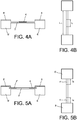
- the Figures 4A and 4B represent a silicon nanowire 1 having in its center a layer 4 of dielectric, which this time is localized.
- the references 8 and 8 'again designate electrical contacts.
- the dielectric zone 4 extends over only part of the length of the nanowire, and over only a thickness of the latter.
- FIG. 5A and 5B shows a device in which an insulating layer 4, 4 'is placed near each recess 6, 6' of the nanowire.
- the total length of the insulating layers is less than the length of the nanowire (condition C2 above), the thickness of each of them is also less than the thickness of the nanowire (condition C1).
- the electrical contacts are also designated by the references 8, 8 '.
- a nanowire structure according to the invention can be used in a more complex structure with a mass such as that of figures 9A - 9C .
- FIGS. 9B and 9C are sectional views along the planes AA 'and BB' of the figure 9A .
- This structure comprises a central part 30, forming a vibrating mass outside of its plane.
- it is, in top view, of substantially rectangular shape connected to each of the two embedding zones 6, 6 'by two arms 33, 33', 35, 35 '.
- top view is possible, for example circular or elliptical, again with arms.
- Each arm is in fact made up of a nanowire according to the present invention.
- One end of each nanowire is connected to the fixed part 6, 6 'of the device, by conductive zones 8, 8', 18, 18 ', as in the previous examples.
- the mass 30 itself contains a dielectric portion 34, over the entire thickness of the mass, and which separates the device into two parts 30 ′, 30 ", each of these parts forming a measurement zone with the two nanowires 33, 33 'and 35, 35' connected to it.
- the rest of the mass 30 is made of conductive material.
- figure 9C that, in the central part, the dielectric portion 34 is extended by dielectric zones 34 ', 34 "of thickness less than zone 34 which can be arranged in continuity with the dielectric zones 4, 4' of the nanowires.
- figure 9C appears the structure of each of the two nanowires 33 ', 35' of the figure 9A : each of these two nanowires has a dielectric layer 4, 4 'and a conductive layer 2.2'.
- one or more nanowires can be associated or connected to one or more masses, for example according to a network. This makes it possible to increase the capture surface for mass measurement applications or to increase the inertial mass in the case of an inertial force sensor.
- a nanowire according to the invention internal constraints can appear, due to differences between the mesh parameters of the conductor 2 and of the dielectric 4 and due to the difference between the thermal expansion coefficients of each of these materials. These constraints can be controlled, in order to obtain nanowires in tension. This control can be produced for example by controlling the deposition temperature or temperatures, and by controlling the relative thicknesses of different layers.
- a nanowire according to the invention can therefore offer higher rigidity and a higher resonant frequency than a nanowire produced solely from silicon. This generally applies to any device according to the invention.
- the second type of device according to the invention uses a metallic material 2, preferably with a low gauge factor G (approximately 2).
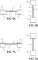
- a metallic nanowire is shown, the center of which 4 is made of an insulating material, for example of intrinsic silicon, or of an insulator such as SiN.
- the two conditions (C1) and (C2) above are satisfied: the dielectric zone extends over only part of the length of the nanowire, and only over a thickness of the latter.
- Figures 11A and 11B represents a device in which the nanowire is partially insulating in its thickness, by nitriding, in a zone 4, 4 'close to the embedments 6, 6'.
- the electrical contacts are also designated by the references 8, 8 '.
- the structure of a device according to the invention can be more complex. It can have the form of that which would be obtained according to the figures 9A-9C replacing any reference to a piezoresistive part with a metallic part.
- the mass 30 also plays the role of vibrating mass.
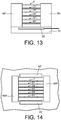
- Such a network can take different forms, with variable steps or with fixed steps, as will be explained in connection with the figures 13 to 15 .
- a device comprises a plurality of nanowires 1, 21, 31, .... according to the invention, arranged parallel to each other, each of the two ends of each nanowire being connected to a stud 60, 60 'or to part of a substrate.
- the current flowing in the wires enters through the pad 60 and exits through the pad 60 '.
- Each of these devices comprises at least one control electrode 22, 22 ′ parallel to the nanowires.
- the network represented in figure 13 is of vertical type, that is to say perpendicular to the plane of a plate or of a substrate 70 forming a support.
- the network represented in figures 14 and 15 is of the horizontal type, that is to say that the nanowires form a two-dimensional network located in the plane of a wafer or of a substrate 20, and in which or in which they may have been formed.
- the references 22, 22 ′ designate two control electrodes, disposed on either side of the network of nanowires, parallel to these. The current flowing in the wires enters through zone 600 and exits through zone 600 '.
- the nanowires are of increasing lengths as a function of a direction perpendicular to the nanowires. We can then address each nanowire individually because each of them has a different frequency from that of the other nanowires. Each nanowire can detect different chemical species by selective functionalization. Each of the species will correspond to a given frequency.
- Means for actuating a nanowire according to the invention comprise for example means of the electrostatic type.
- the actuation means may comprise means of the thermoelastic type or of the magnetic type or any other means. Such means make it possible to give the nanowire a movement in a direction perpendicular to its direction of extension.
- Electrostatic actuation uses the electrostatic force generated between electrode 22 (or 22 ') and the nanowire (s) by applying a potential difference.
- Thermoelastic actuation can be used when the two layers (metallic and insulating) are the same length, equal to that of the nanowire. This type of actuation exploits the heating effect in each of the layers.
- the layers being of different natures, the dilations are different, which generates a bending moment and therefore a movement of the nanowire.
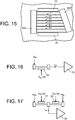
- a device according to the invention can implement means for reading the variation in resistance of the nanowire (s). Examples of such means will be given in figures 16 - 18 .
- the variation in resistance at the terminals of the nanowire (s) can be measured directly through the modulation of the current I which passes through it, at constant reading voltage.
- a constant voltage V dc is applied across the nanowire.
- the reference 50 symbolizes an excitation electrode to which an alternating voltage V ac is applied.
- the output signal, a current i ac is connected to an amplifier 52.
- the diagram of the figure 17 represents a direct measurement with a half bridge.
- the nanowire is under a constant voltage V dc .
- the electrodes 51 and 53 make it possible to apply to one of the parts of the wires an alternating voltage of frequency ⁇ .
- the outgoing alternating current iac, taken between the two parts of the bridge is sent to an amplifier 52.
- a heterodyning technique represented schematically in figure 18 , brings the resistance measurement from high frequencies to low frequencies.
- This technique can be used both for direct measurement and for differential measurement by bridge.
- This technique we can refer to I. Bargatin et al. "Applied Physics Letters", vol. 86, 133109 (2005 ).
- the alternating voltages can be generated with local oscillators.
- the reading system can be integrated (structured on the same chip) or placed on an external ASIC.
- the transduction (the creation of a current by the movement of the nanowire) is carried out through the nanowire, this one is therefore used both as proof mass (mobile part) and as a gauge element to achieve the desired piezoresistive conversion.
- a device therefore makes it possible to know the variation in resistance ⁇ R, linked to the variation in stress ( ⁇ ) induced by the vibration of the nanowire, because ⁇ R is proportional to the stress.
- p is the resistivity of the medium formed by the bar
- ⁇ L is the relative elongation of the bar of which S and L are the length and the section respectively.
- ⁇ is the Poisson's ratio.
- the first term (dp / p) corresponds to the piezoresistive effect proper, while the second ( ⁇ L (1 + 2 ⁇ )) corresponds to a purely geometric effect.
- the second term is several orders of magnitude less than the first.
- Piezoresistivity is a physical phenomenon that links a relative variation in resistivity d ⁇ ⁇ to a stress applied to the piezoresistive material, which is here a nanowire.
- ⁇ ij are the piezoresistivity tensor elements expressed along the main crystalline axes of the semiconductor.
- ⁇ L and ⁇ T are respectively the longitudinal piezoresistive coefficient and the transverse piezoresistive coefficient expressed in a main reference (N, T) of the nanowire (see figure 19 ), N being in the direction of the nanowire, T being in a transverse direction.
- ⁇ L and ⁇ T are the applied longitudinal and transverse stresses respectively, as illustrated on the figure 19 .
- I is the quadratic moment
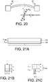
- M the bending moment represented in figure 20
- y is the ordinate, taking the neutral fiber, along which the stresses are zero (dotted line on the figure 20 ) as origin.
- the average stress on the section of the nanowire is zero.
- FIG 21A of rectangular section composed of a part 102 of lightly doped silicon, of thickness t 2 (for example doping is approximately 10 15 cm -3 to 10 19 cm -3 ) and a portion 104 nitrided SiN thickness t 1 piezoresistive.
- the nitrided part 104 here has a thickness t 1 greater than the silicon part 102 (thickness t 2 ) in order to concentrate the stress.
- the thickness of the Si layer becomes negligible compared to that of SiN, and the stress in Si is then maximum and equal to the stress calculated on the external fiber of the SiN layer.
- ⁇ L is the elongation of the gauge
- G is the gauge factor (of the order of several thousands (for example for a Si nanowire doped with Boron at 10 15 .cm -3 ).
- G is of the order of a few units (typically 2 for metals).
- a silicon wafer 200 is selected.
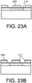
- figure 22B two epitaxies are carried out successively of a layer 202 of SiGe and of a layer 204 of Si.
- the proportion of germanium in layer 202 SiGe can be fixed at a given value; it can also be variable in this layer, which induces therein a variation of the initial stress. We can therefore adjust this initial constraint by controlling the proportion of germanium.
- an actuation electrode can be structured.
- This nanobeam is then released by tunnel etching of the layer of SiGe 204, which is illustrated, according to two views, in figures 22D and 22E .
- the view from the figure 22E is a side view according to arrow A of the figure 22C .
- the section of the nanobeam is reduced to form one or more nanowires 210 ( figures 22F and 22G , respectively from figures 22D and 22E ), until these reach a diameter or a dimension, according to a section, of the order of 25 nm or, more generally, between 10 and 30 nm.
- the oxide deposit made above the nanowires can then undergo lithography and etching operations ( figure 22I ), in order to clear areas of access to the nanowire in order to transform certain selected areas.
- the technique used can be an annealing technique which does not induce a reaction in the oxide.
- the oxide 208 above the wire is removed; the removal of SiN on the oxide can be carried out wet.
- the contact zones can be thickened and made metallic by doping and / or siliciding and / or metallization.
- the nanowire is released, by etching the oxide 208 placed in the cavity in contact with the substrate ( figure 22L ).
- the first two steps of this process can be omitted using an SOI plate.
- an oxide etching is carried out in place of the etching of the SiGe layer.
- the Liberation ( figure 22D ) is then done by HF steam.
- siliciding by diffusing the metal from the cleared portions of the nanowire, over a thickness of 6 nm for example.
- the technique used is an annealing technique which does not induce a reaction in the oxide.
- the siliciding process can be replaced by doping (up to amorphization).
- the oxide 208 is removed above the nanowire; the removal of NiSi on the oxide can be carried out wet. Finally, the nanowire is released, by etching the oxide placed in the cavity 220 in contact with the substrate 200 ( figure 23E ).
- the first two steps can be omitted using an SOI plate.
- the release is then, again, by HF steam.
- a bilayer consisting of a layer 302 of SiO2 or of SiGe or of Si and of a layer 304 of SiGe or of Si is produced ( figure 24A ).
- a layer of resin can be formed above of this bilayer and then etched to form patterns 306 which will allow etching of the layer 302 ( figure 24B ).
- Annealing optionally makes it possible to round off the tops of the pads 308, 310 of Si thus produced.
- a succession of annealing and / or oxidation steps can be carried out in order to round off and reduce the section of the nanowire.
- One or more annealing and / or oxidation steps makes it possible to round the nanowires, hence a reduction in the section of these nanowires, to a diameter of approximately 5 nm for example. Recrystallization can be obtained by annealing.
- the measuring means can be produced by an external circuit.
- the actuation for example electrostatic, is carried out by means of a gap between the substrate and the nanowire after release of the nanowire. It is preferably made by engraving a gap "Lateral" between the nanowire and an electrode, during the etching step to define the nanowire.
- the nanowire can be vibrated by the use of actuation means comprising a lateral electrode and an electrode under the nanowire.
- a sensor according to the invention can be used as a chemical sensor (such an application with another sensor is described in Y. Wims et al. “Sensors and Actuators” B 108 (2005 )), in the gas phase or in the liquid phase or as molecular force sensors (such an application with another sensor is described in JL Arlett et al. "Nobel Symposium", 131 (2006 )), or in the field of mass spectrometry (such an application with another sensor is described in W. Jensen et al. "Nature Nanotechnology” 9, 533 (2008 )).
- one or more sensitive zones can be located, thereby improving the transduction efficiency.
- a first order effect is obtained in the semiconductor, hence an increased detection effect compared to known techniques, in particular described in the document. WO 2005/106417 .
Landscapes
- Engineering & Computer Science (AREA)
- Computer Hardware Design (AREA)
- Microelectronics & Electronic Packaging (AREA)
- Micromachines (AREA)
- Pressure Sensors (AREA)
Claims (9)
- Sensorvorrichtung vom Typ mit Nanodraht, enthaltend:- eine Vielzahl von Nanodrähten, die parallel zueinander angeordnet sind, wobei die Nanodrähte in einer Richtung senkrecht zu den Nanodrähten eine zunehmende Länge aufweisen, wobei jeder Nanodraht eine erste leitende Zone (2) und eine zweite Zone (4, 4') aus isolierendem Material enthält, wobei diese zweite Zone nicht die gesamte Dicke des Nanodrahts einnimmt und ein Strom durch diesen von einem seiner Enden zum anderen fließen kann;- und zwei feste Haltezonen (60, 60', 600, 600'), an denen die Enden jedes Nanodrahts befestigt sind.
- Vorrichtung nach Anspruch 1,
wobei die zweite Zone jedes Nanodrahtes sich über eine Länge erstreckt, die geringer als die des Nanodrahts ist. - Vorrichtung nach Anspruch 1 oder 2
wobei der leitende Abschnitt jedes Nanodrahts- aus einem dotierten Halbleitermaterial, beispielsweise aus einem piezoresistiven Material, besteht, wobei der Halbleiter mit Arsen, Bor oder Phosphor dotiert sein kann;- oder aus einem metallischen Material, beispielsweise aus einem Silicid-Metall, wie etwa NiSi oder WSi oder PtSi, besteht. - Vorrichtung nach einem der Ansprüche 1 bis 3,
wobei das Isoliermaterial des Nanodrahtes ein dielektrisches Material, beispielsweise aus Silizium- oder Aluminiumnitrid oder aus Siliciumoxid, oder ein intrinsisches Halbleitermaterial, beispielsweise Silizium oder eine Legierung aus Silizium und Germanium (SiGe), die undotiert sind, ist. - Vorrichtung nach einem der Ansprüche 1 bis 4,
wobei der Nanodraht enthält:- eine dielektrische Zone (4) aus undotiertem SiGe und eine leitende Zone (2) aus dotiertem Si,- oder eine dielektrische Zone (4) aus undotiertem Si und eine leitende Zone (2) aus dotiertem SiGe. - Vorrichtung nach einem der Ansprüche 1 bis 5,
ferner enthaltend Wandlerelemente, die Bewegungen von mindestens einem Nanodraht in ein elektrisches Signal umsetzen. - Vorrichtung nach einem der Ansprüche 1 bis 6,
ferner enthaltend
Mittel (22, 22') zur Betätigung eines jeden Nanodrahtes, wobei diese Mittel zur Betätigung des Nanodrahts beispielsweise vom elektrostatischen Typ oder vom thermoelastischen Typ oder vom magnetischen Typ sind. - Vorrichtung nach einem der Ansprüche 1 bis 7,
wobei die Vielzahl von Nanodrähten ein vertikales Array bildet, das senkrecht zur Ebene eines Wafers oder Trägersubstrats (70) verläuft. - Vorrichtung nach einem der Ansprüche 1 bis 7,
wobei die Vielzahl von Nanodrähten ein horizontales Array in der Ebene eines Wafers oder Substrats (20) bildet.
Applications Claiming Priority (2)
| Application Number | Priority Date | Filing Date | Title |
|---|---|---|---|
| FR0951251A FR2942660B1 (fr) | 2009-02-27 | 2009-02-27 | Dispositif capteur a base de nanofils |
| EP10154557.2A EP2223887B1 (de) | 2009-02-27 | 2010-02-24 | Sensor mit Nanodrähten |
Related Parent Applications (2)
| Application Number | Title | Priority Date | Filing Date |
|---|---|---|---|
| EP10154557.2A Division EP2223887B1 (de) | 2009-02-27 | 2010-02-24 | Sensor mit Nanodrähten |
| EP10154557.2A Division-Into EP2223887B1 (de) | 2009-02-27 | 2010-02-24 | Sensor mit Nanodrähten |
Publications (2)
| Publication Number | Publication Date |
|---|---|
| EP3424875A1 EP3424875A1 (de) | 2019-01-09 |
| EP3424875B1 true EP3424875B1 (de) | 2020-04-15 |
Family
ID=41465391
Family Applications (3)
| Application Number | Title | Priority Date | Filing Date |
|---|---|---|---|
| EP18187837.2A Active EP3424874B1 (de) | 2009-02-27 | 2010-02-24 | Sensorvorrichtung auf der basis von nanodrähten mit einer mobilen masse |
| EP18187843.0A Active EP3424875B1 (de) | 2009-02-27 | 2010-02-24 | Sensorvorrichtung auf der basis von nanodrähten mit zunehmender länge |
| EP10154557.2A Active EP2223887B1 (de) | 2009-02-27 | 2010-02-24 | Sensor mit Nanodrähten |
Family Applications Before (1)
| Application Number | Title | Priority Date | Filing Date |
|---|---|---|---|
| EP18187837.2A Active EP3424874B1 (de) | 2009-02-27 | 2010-02-24 | Sensorvorrichtung auf der basis von nanodrähten mit einer mobilen masse |
Family Applications After (1)
| Application Number | Title | Priority Date | Filing Date |
|---|---|---|---|
| EP10154557.2A Active EP2223887B1 (de) | 2009-02-27 | 2010-02-24 | Sensor mit Nanodrähten |
Country Status (4)
| Country | Link |
|---|---|
| US (1) | US9382108B2 (de) |
| EP (3) | EP3424874B1 (de) |
| JP (1) | JP2010204098A (de) |
| FR (1) | FR2942660B1 (de) |
Families Citing this family (8)
| Publication number | Priority date | Publication date | Assignee | Title |
|---|---|---|---|---|
| FR2923646A1 (fr) * | 2007-11-09 | 2009-05-15 | Commissariat Energie Atomique | Cellule memoire sram dotee de transistors a structure multi-canaux verticale |
| FR2995691B1 (fr) * | 2012-09-19 | 2014-10-10 | Commissariat Energie Atomique | Capteur de flux thermique, capteur de gaz comportant au moins un tel capteur et jauge pirani comportant au moins un tel capteur |
| WO2014169960A1 (en) * | 2013-04-19 | 2014-10-23 | Koc Universitesi | A nanomechanical resonator array and production method thereof |
| FR3017463B1 (fr) | 2014-02-13 | 2020-11-13 | Commissariat Energie Atomique | Capteur de concentration de gaz a structure suspendue |
| WO2017170748A1 (ja) * | 2016-03-31 | 2017-10-05 | 京セラ株式会社 | 応力センサ |
| KR101919344B1 (ko) | 2016-12-26 | 2018-11-20 | 한양대학교 에리카산학협력단 | 산화아연 습도센서 소자 제조방법 |
| FR3086386B1 (fr) * | 2018-09-21 | 2020-12-04 | Commissariat Energie Atomique | Dispositif de mesure comportant un fil semiconducteur suspendu |
| FR3110284B1 (fr) * | 2020-05-14 | 2023-01-13 | Commissariat Energie Atomique | Dispositif de détection utilisant une transduction piézorésistive |
Family Cites Families (7)
| Publication number | Priority date | Publication date | Assignee | Title |
|---|---|---|---|---|
| WO2002080360A1 (en) * | 2001-03-30 | 2002-10-10 | California Institute Of Technology | Pattern-aligned carbon nanotube growth and tunable resonator apparatus |
| US7051945B2 (en) * | 2002-09-30 | 2006-05-30 | Nanosys, Inc | Applications of nano-enabled large area macroelectronic substrates incorporating nanowires and nanowire composites |
| US7302856B2 (en) * | 2003-05-07 | 2007-12-04 | California Institute Of Technology | Strain sensors based on nanowire piezoresistor wires and arrays |
| US7473943B2 (en) * | 2004-10-15 | 2009-01-06 | Nanosys, Inc. | Gate configuration for nanowire electronic devices |
| FR2884648B1 (fr) | 2005-04-13 | 2007-09-07 | Commissariat Energie Atomique | Structure et procede de realisation d'un dispositif microelectronique dote d'un ou plusieurs fils quantiques aptes a former un canal ou plusieurs canaux de transistors |
| AT503995B1 (de) * | 2006-08-07 | 2009-03-15 | Arc Seibersdorf Res Gmbh | Miniatur-beschleunigungssensor |
| US7819005B2 (en) * | 2007-06-25 | 2010-10-26 | Micron Technology, Inc. | Sensor and transducer devices comprising carbon nanotubes, methods of making and using the same |
-
2009
- 2009-02-27 FR FR0951251A patent/FR2942660B1/fr not_active Expired - Fee Related
-
2010
- 2010-02-24 EP EP18187837.2A patent/EP3424874B1/de active Active
- 2010-02-24 EP EP18187843.0A patent/EP3424875B1/de active Active
- 2010-02-24 EP EP10154557.2A patent/EP2223887B1/de active Active
- 2010-02-26 US US12/713,909 patent/US9382108B2/en active Active
- 2010-02-26 JP JP2010041878A patent/JP2010204098A/ja active Pending
Non-Patent Citations (1)
| Title |
|---|
| None * |
Also Published As
| Publication number | Publication date |
|---|---|
| EP2223887A1 (de) | 2010-09-01 |
| FR2942660A1 (fr) | 2010-09-03 |
| JP2010204098A (ja) | 2010-09-16 |
| FR2942660B1 (fr) | 2011-04-01 |
| EP3424875A1 (de) | 2019-01-09 |
| EP3424874A1 (de) | 2019-01-09 |
| EP2223887B1 (de) | 2018-09-12 |
| EP3424874B1 (de) | 2020-09-30 |
| US20100219489A1 (en) | 2010-09-02 |
| US9382108B2 (en) | 2016-07-05 |
Similar Documents
| Publication | Publication Date | Title |
|---|---|---|
| EP3424875B1 (de) | Sensorvorrichtung auf der basis von nanodrähten mit zunehmender länge | |
| EP2617129B1 (de) | Vorrichtung mit freihängendem träger und piezoresistive vorrichtung zur verlagerungserkennung | |
| EP2309559B1 (de) | Piezoelektrische Erregerstruktur mit integriertem piezoresistivem Dehnmessstreifen und Herstellungsverfahren dafür | |
| EP2008965B1 (de) | Resonanzvorrichtung mit piezoelektrischer Erfassung für den Einsatz in Oberflächentechnologien | |
| EP2211185B1 (de) | Trägheitssensor oder Resonanzsensor in der Oberflächentechnologie zur Erkennung von Abweichungen mit Hilfe eines Dehnungsmessers | |
| FR2948114A1 (fr) | Nems comportant des moyens de transduction a base d'alliage d'aluminium | |
| EP2367015B1 (de) | Rauscharmer kraftsensor | |
| EP2617130B1 (de) | Resonanter piezoresistiver detektor mit einem an das trägerelement des detektors elastisch angeschlossenen resonator und verfahren zur herstellung dieses detektors | |
| EP2491406B1 (de) | Sensor für piezoresistive detektion auf gleicher ebene | |
| EP0766060B1 (de) | Herstellung eines mikromechanischen Teils mit mindestens einer Diamantspitze. | |
| EP2211143B1 (de) | Planarer mikromechanischer Kreisel mit Messung ausserhalb der Ebene mittels Dehnungsmesser | |
| EP2616386B1 (de) | In der ebene betätigte resonanzvorrichtung und verfahren zur herstellung der vorrichtung | |
| EP2267893B1 (de) | Volumenwellenresonator mit teilweise gefüllten Kavitäten | |
| FR2950332A1 (fr) | Realisation d'un composant electromecanique pour un micro- ou nano- systeme dote d'un barreau formant un axe de rotation du composant et recouvert de graphene | |
| EP2949621B1 (de) | Kapazitive mikro- und/ oder nanoelektronische Vorrichtung mit erhöhter Kompaktheit | |
| EP1895270B1 (de) | Mikrosystem, insbesondere Mikro-Gyroskop, mit Detektionselement mit kapazitiven Elektroden | |
| EP2866020B1 (de) | Vorrichtung zur elektromechanischen Erfassung, zur gravimetrischen Erfassung | |
| EP2862000B1 (de) | Sensor für magnetfelder mit laplace-kraft | |
| FR2871790A1 (fr) | Microressort de grande amplitude | |
| FR3087006A1 (fr) | Dispositif de detection pyroelectrique a membrane suspendue | |
| FR2973608A1 (fr) | Procede d'ajustement de la frequence de resonance d'un element vibrant micro-usine | |
| FR3089630A1 (fr) | Capteur de flux thermique a nanofilaments chauffants |
Legal Events
| Date | Code | Title | Description |
|---|---|---|---|
| PUAI | Public reference made under article 153(3) epc to a published international application that has entered the european phase |
Free format text: ORIGINAL CODE: 0009012 |
|
| STAA | Information on the status of an ep patent application or granted ep patent |
Free format text: STATUS: REQUEST FOR EXAMINATION WAS MADE |
|
| 17P | Request for examination filed |
Effective date: 20180807 |
|
| AC | Divisional application: reference to earlier application |
Ref document number: 2223887 Country of ref document: EP Kind code of ref document: P |
|
| AK | Designated contracting states |
Kind code of ref document: A1 Designated state(s): AT BE BG CH CY CZ DE DK EE ES FI FR GB GR HR HU IE IS IT LI LT LU LV MC MK MT NL NO PL PT RO SE SI SK SM TR |
|
| GRAP | Despatch of communication of intention to grant a patent |
Free format text: ORIGINAL CODE: EPIDOSNIGR1 |
|
| STAA | Information on the status of an ep patent application or granted ep patent |
Free format text: STATUS: GRANT OF PATENT IS INTENDED |
|
| RIC1 | Information provided on ipc code assigned before grant |
Ipc: B81B 3/00 20060101AFI20191028BHEP |
|
| INTG | Intention to grant announced |
Effective date: 20191121 |
|
| GRAS | Grant fee paid |
Free format text: ORIGINAL CODE: EPIDOSNIGR3 |
|
| GRAA | (expected) grant |
Free format text: ORIGINAL CODE: 0009210 |
|
| STAA | Information on the status of an ep patent application or granted ep patent |
Free format text: STATUS: THE PATENT HAS BEEN GRANTED |
|
| AC | Divisional application: reference to earlier application |
Ref document number: 2223887 Country of ref document: EP Kind code of ref document: P |
|
| AK | Designated contracting states |
Kind code of ref document: B1 Designated state(s): AT BE BG CH CY CZ DE DK EE ES FI FR GB GR HR HU IE IS IT LI LT LU LV MC MK MT NL NO PL PT RO SE SI SK SM TR |
|
| REG | Reference to a national code |
Ref country code: CH Ref legal event code: EP |
|
| REG | Reference to a national code |
Ref country code: DE Ref legal event code: R096 Ref document number: 602010063973 Country of ref document: DE |
|
| REG | Reference to a national code |
Ref country code: IE Ref legal event code: FG4D Free format text: LANGUAGE OF EP DOCUMENT: FRENCH |
|
| REG | Reference to a national code |
Ref country code: AT Ref legal event code: REF Ref document number: 1257071 Country of ref document: AT Kind code of ref document: T Effective date: 20200515 |
|
| REG | Reference to a national code |
Ref country code: NL Ref legal event code: MP Effective date: 20200415 |
|
| REG | Reference to a national code |
Ref country code: LT Ref legal event code: MG4D |
|
| PG25 | Lapsed in a contracting state [announced via postgrant information from national office to epo] |
Ref country code: NL Free format text: LAPSE BECAUSE OF FAILURE TO SUBMIT A TRANSLATION OF THE DESCRIPTION OR TO PAY THE FEE WITHIN THE PRESCRIBED TIME-LIMIT Effective date: 20200415 Ref country code: PT Free format text: LAPSE BECAUSE OF FAILURE TO SUBMIT A TRANSLATION OF THE DESCRIPTION OR TO PAY THE FEE WITHIN THE PRESCRIBED TIME-LIMIT Effective date: 20200817 Ref country code: LT Free format text: LAPSE BECAUSE OF FAILURE TO SUBMIT A TRANSLATION OF THE DESCRIPTION OR TO PAY THE FEE WITHIN THE PRESCRIBED TIME-LIMIT Effective date: 20200415 Ref country code: GR Free format text: LAPSE BECAUSE OF FAILURE TO SUBMIT A TRANSLATION OF THE DESCRIPTION OR TO PAY THE FEE WITHIN THE PRESCRIBED TIME-LIMIT Effective date: 20200716 Ref country code: NO Free format text: LAPSE BECAUSE OF FAILURE TO SUBMIT A TRANSLATION OF THE DESCRIPTION OR TO PAY THE FEE WITHIN THE PRESCRIBED TIME-LIMIT Effective date: 20200715 Ref country code: FI Free format text: LAPSE BECAUSE OF FAILURE TO SUBMIT A TRANSLATION OF THE DESCRIPTION OR TO PAY THE FEE WITHIN THE PRESCRIBED TIME-LIMIT Effective date: 20200415 Ref country code: IS Free format text: LAPSE BECAUSE OF FAILURE TO SUBMIT A TRANSLATION OF THE DESCRIPTION OR TO PAY THE FEE WITHIN THE PRESCRIBED TIME-LIMIT Effective date: 20200815 Ref country code: SE Free format text: LAPSE BECAUSE OF FAILURE TO SUBMIT A TRANSLATION OF THE DESCRIPTION OR TO PAY THE FEE WITHIN THE PRESCRIBED TIME-LIMIT Effective date: 20200415 |
|
| REG | Reference to a national code |
Ref country code: AT Ref legal event code: MK05 Ref document number: 1257071 Country of ref document: AT Kind code of ref document: T Effective date: 20200415 |
|
| PG25 | Lapsed in a contracting state [announced via postgrant information from national office to epo] |
Ref country code: HR Free format text: LAPSE BECAUSE OF FAILURE TO SUBMIT A TRANSLATION OF THE DESCRIPTION OR TO PAY THE FEE WITHIN THE PRESCRIBED TIME-LIMIT Effective date: 20200415 Ref country code: BG Free format text: LAPSE BECAUSE OF FAILURE TO SUBMIT A TRANSLATION OF THE DESCRIPTION OR TO PAY THE FEE WITHIN THE PRESCRIBED TIME-LIMIT Effective date: 20200715 Ref country code: LV Free format text: LAPSE BECAUSE OF FAILURE TO SUBMIT A TRANSLATION OF THE DESCRIPTION OR TO PAY THE FEE WITHIN THE PRESCRIBED TIME-LIMIT Effective date: 20200415 |
|
| REG | Reference to a national code |
Ref country code: DE Ref legal event code: R097 Ref document number: 602010063973 Country of ref document: DE |
|
| PG25 | Lapsed in a contracting state [announced via postgrant information from national office to epo] |
Ref country code: ES Free format text: LAPSE BECAUSE OF FAILURE TO SUBMIT A TRANSLATION OF THE DESCRIPTION OR TO PAY THE FEE WITHIN THE PRESCRIBED TIME-LIMIT Effective date: 20200415 Ref country code: CZ Free format text: LAPSE BECAUSE OF FAILURE TO SUBMIT A TRANSLATION OF THE DESCRIPTION OR TO PAY THE FEE WITHIN THE PRESCRIBED TIME-LIMIT Effective date: 20200415 Ref country code: AT Free format text: LAPSE BECAUSE OF FAILURE TO SUBMIT A TRANSLATION OF THE DESCRIPTION OR TO PAY THE FEE WITHIN THE PRESCRIBED TIME-LIMIT Effective date: 20200415 Ref country code: DK Free format text: LAPSE BECAUSE OF FAILURE TO SUBMIT A TRANSLATION OF THE DESCRIPTION OR TO PAY THE FEE WITHIN THE PRESCRIBED TIME-LIMIT Effective date: 20200415 Ref country code: SM Free format text: LAPSE BECAUSE OF FAILURE TO SUBMIT A TRANSLATION OF THE DESCRIPTION OR TO PAY THE FEE WITHIN THE PRESCRIBED TIME-LIMIT Effective date: 20200415 Ref country code: EE Free format text: LAPSE BECAUSE OF FAILURE TO SUBMIT A TRANSLATION OF THE DESCRIPTION OR TO PAY THE FEE WITHIN THE PRESCRIBED TIME-LIMIT Effective date: 20200415 Ref country code: RO Free format text: LAPSE BECAUSE OF FAILURE TO SUBMIT A TRANSLATION OF THE DESCRIPTION OR TO PAY THE FEE WITHIN THE PRESCRIBED TIME-LIMIT Effective date: 20200415 Ref country code: IT Free format text: LAPSE BECAUSE OF FAILURE TO SUBMIT A TRANSLATION OF THE DESCRIPTION OR TO PAY THE FEE WITHIN THE PRESCRIBED TIME-LIMIT Effective date: 20200415 |
|
| PLBE | No opposition filed within time limit |
Free format text: ORIGINAL CODE: 0009261 |
|
| STAA | Information on the status of an ep patent application or granted ep patent |
Free format text: STATUS: NO OPPOSITION FILED WITHIN TIME LIMIT |
|
| PG25 | Lapsed in a contracting state [announced via postgrant information from national office to epo] |
Ref country code: PL Free format text: LAPSE BECAUSE OF FAILURE TO SUBMIT A TRANSLATION OF THE DESCRIPTION OR TO PAY THE FEE WITHIN THE PRESCRIBED TIME-LIMIT Effective date: 20200415 Ref country code: SK Free format text: LAPSE BECAUSE OF FAILURE TO SUBMIT A TRANSLATION OF THE DESCRIPTION OR TO PAY THE FEE WITHIN THE PRESCRIBED TIME-LIMIT Effective date: 20200415 |
|
| 26N | No opposition filed |
Effective date: 20210118 |
|
| PG25 | Lapsed in a contracting state [announced via postgrant information from national office to epo] |
Ref country code: SI Free format text: LAPSE BECAUSE OF FAILURE TO SUBMIT A TRANSLATION OF THE DESCRIPTION OR TO PAY THE FEE WITHIN THE PRESCRIBED TIME-LIMIT Effective date: 20200415 |
|
| PG25 | Lapsed in a contracting state [announced via postgrant information from national office to epo] |
Ref country code: MC Free format text: LAPSE BECAUSE OF FAILURE TO SUBMIT A TRANSLATION OF THE DESCRIPTION OR TO PAY THE FEE WITHIN THE PRESCRIBED TIME-LIMIT Effective date: 20200415 |
|
| REG | Reference to a national code |
Ref country code: BE Ref legal event code: MM Effective date: 20210228 |
|
| PG25 | Lapsed in a contracting state [announced via postgrant information from national office to epo] |
Ref country code: CH Free format text: LAPSE BECAUSE OF NON-PAYMENT OF DUE FEES Effective date: 20210228 Ref country code: LI Free format text: LAPSE BECAUSE OF NON-PAYMENT OF DUE FEES Effective date: 20210228 Ref country code: LU Free format text: LAPSE BECAUSE OF NON-PAYMENT OF DUE FEES Effective date: 20210224 |
|
| PG25 | Lapsed in a contracting state [announced via postgrant information from national office to epo] |
Ref country code: IE Free format text: LAPSE BECAUSE OF NON-PAYMENT OF DUE FEES Effective date: 20210224 |
|
| PG25 | Lapsed in a contracting state [announced via postgrant information from national office to epo] |
Ref country code: BE Free format text: LAPSE BECAUSE OF NON-PAYMENT OF DUE FEES Effective date: 20210228 |
|
| PG25 | Lapsed in a contracting state [announced via postgrant information from national office to epo] |
Ref country code: CY Free format text: LAPSE BECAUSE OF FAILURE TO SUBMIT A TRANSLATION OF THE DESCRIPTION OR TO PAY THE FEE WITHIN THE PRESCRIBED TIME-LIMIT Effective date: 20200415 |
|
| PG25 | Lapsed in a contracting state [announced via postgrant information from national office to epo] |
Ref country code: HU Free format text: LAPSE BECAUSE OF FAILURE TO SUBMIT A TRANSLATION OF THE DESCRIPTION OR TO PAY THE FEE WITHIN THE PRESCRIBED TIME-LIMIT; INVALID AB INITIO Effective date: 20100224 |
|
| PG25 | Lapsed in a contracting state [announced via postgrant information from national office to epo] |
Ref country code: MK Free format text: LAPSE BECAUSE OF FAILURE TO SUBMIT A TRANSLATION OF THE DESCRIPTION OR TO PAY THE FEE WITHIN THE PRESCRIBED TIME-LIMIT Effective date: 20200415 |
|
| PG25 | Lapsed in a contracting state [announced via postgrant information from national office to epo] |
Ref country code: TR Free format text: LAPSE BECAUSE OF FAILURE TO SUBMIT A TRANSLATION OF THE DESCRIPTION OR TO PAY THE FEE WITHIN THE PRESCRIBED TIME-LIMIT Effective date: 20200415 |
|
| PG25 | Lapsed in a contracting state [announced via postgrant information from national office to epo] |
Ref country code: MT Free format text: LAPSE BECAUSE OF FAILURE TO SUBMIT A TRANSLATION OF THE DESCRIPTION OR TO PAY THE FEE WITHIN THE PRESCRIBED TIME-LIMIT Effective date: 20200415 |
|
| PGFP | Annual fee paid to national office [announced via postgrant information from national office to epo] |
Ref country code: DE Payment date: 20250218 Year of fee payment: 16 |
|
| PGFP | Annual fee paid to national office [announced via postgrant information from national office to epo] |
Ref country code: FR Payment date: 20250219 Year of fee payment: 16 |
|
| PGFP | Annual fee paid to national office [announced via postgrant information from national office to epo] |
Ref country code: GB Payment date: 20250218 Year of fee payment: 16 |