EP3425434A1 - Dispositif optique - Google Patents
Dispositif optique Download PDFInfo
- Publication number
- EP3425434A1 EP3425434A1 EP17759744.0A EP17759744A EP3425434A1 EP 3425434 A1 EP3425434 A1 EP 3425434A1 EP 17759744 A EP17759744 A EP 17759744A EP 3425434 A1 EP3425434 A1 EP 3425434A1
- Authority
- EP
- European Patent Office
- Prior art keywords
- optical
- filters
- pass
- optical signals
- signals
- Prior art date
- Legal status (The legal status is an assumption and is not a legal conclusion. Google has not performed a legal analysis and makes no representation as to the accuracy of the status listed.)
- Withdrawn
Links
- 230000003287 optical effect Effects 0.000 title claims abstract description 451
- 125000004122 cyclic group Chemical group 0.000 claims description 67
- 238000003672 processing method Methods 0.000 claims description 8
- 238000001914 filtration Methods 0.000 claims description 4
- 238000004891 communication Methods 0.000 description 14
- 238000010586 diagram Methods 0.000 description 13
- 230000005540 biological transmission Effects 0.000 description 12
- 230000008878 coupling Effects 0.000 description 6
- 238000010168 coupling process Methods 0.000 description 6
- 238000005859 coupling reaction Methods 0.000 description 6
- 230000012447 hatching Effects 0.000 description 3
- 239000013307 optical fiber Substances 0.000 description 3
- 230000004308 accommodation Effects 0.000 description 2
- 230000003247 decreasing effect Effects 0.000 description 2
- XUIMIQQOPSSXEZ-UHFFFAOYSA-N Silicon Chemical compound [Si] XUIMIQQOPSSXEZ-UHFFFAOYSA-N 0.000 description 1
- 230000002950 deficient Effects 0.000 description 1
- 230000006866 deterioration Effects 0.000 description 1
- 230000002542 deteriorative effect Effects 0.000 description 1
- 230000000694 effects Effects 0.000 description 1
- 238000005516 engineering process Methods 0.000 description 1
- 239000004973 liquid crystal related substance Substances 0.000 description 1
- 238000000034 method Methods 0.000 description 1
- 230000002250 progressing effect Effects 0.000 description 1
- 229910052710 silicon Inorganic materials 0.000 description 1
- 239000010703 silicon Substances 0.000 description 1
Images





Classifications
-
- G—PHYSICS
- G02—OPTICS
- G02B—OPTICAL ELEMENTS, SYSTEMS OR APPARATUS
- G02B5/00—Optical elements other than lenses
- G02B5/18—Diffraction gratings
- G02B5/1866—Transmission gratings characterised by their structure, e.g. step profile, contours of substrate or grooves, pitch variations, materials
-
- G—PHYSICS
- G02—OPTICS
- G02B—OPTICAL ELEMENTS, SYSTEMS OR APPARATUS
- G02B6/00—Light guides; Structural details of arrangements comprising light guides and other optical elements, e.g. couplings
- G02B6/24—Coupling light guides
- G02B6/26—Optical coupling means
- G02B6/28—Optical coupling means having data bus means, i.e. plural waveguides interconnected and providing an inherently bidirectional system by mixing and splitting signals
- G02B6/293—Optical coupling means having data bus means, i.e. plural waveguides interconnected and providing an inherently bidirectional system by mixing and splitting signals with wavelength selective means
- G02B6/29379—Optical coupling means having data bus means, i.e. plural waveguides interconnected and providing an inherently bidirectional system by mixing and splitting signals with wavelength selective means characterised by the function or use of the complete device
- G02B6/29389—Bandpass filtering, e.g. 1x1 device rejecting or passing certain wavelengths
-
- G—PHYSICS
- G02—OPTICS
- G02F—OPTICAL DEVICES OR ARRANGEMENTS FOR THE CONTROL OF LIGHT BY MODIFICATION OF THE OPTICAL PROPERTIES OF THE MEDIA OF THE ELEMENTS INVOLVED THEREIN; NON-LINEAR OPTICS; FREQUENCY-CHANGING OF LIGHT; OPTICAL LOGIC ELEMENTS; OPTICAL ANALOGUE/DIGITAL CONVERTERS
- G02F1/00—Devices or arrangements for the control of the intensity, colour, phase, polarisation or direction of light arriving from an independent light source, e.g. switching, gating or modulating; Non-linear optics
- G02F1/29—Devices or arrangements for the control of the intensity, colour, phase, polarisation or direction of light arriving from an independent light source, e.g. switching, gating or modulating; Non-linear optics for the control of the position or the direction of light beams, i.e. deflection
- G02F1/31—Digital deflection, i.e. optical switching
-
- H—ELECTRICITY
- H04—ELECTRIC COMMUNICATION TECHNIQUE
- H04B—TRANSMISSION
- H04B10/00—Transmission systems employing electromagnetic waves other than radio-waves, e.g. infrared, visible or ultraviolet light, or employing corpuscular radiation, e.g. quantum communication
- H04B10/60—Receivers
-
- H—ELECTRICITY
- H04—ELECTRIC COMMUNICATION TECHNIQUE
- H04J—MULTIPLEX COMMUNICATION
- H04J14/00—Optical multiplex systems
- H04J14/02—Wavelength-division multiplex systems
- H04J14/0201—Add-and-drop multiplexing
- H04J14/0202—Arrangements therefor
-
- G—PHYSICS
- G02—OPTICS
- G02B—OPTICAL ELEMENTS, SYSTEMS OR APPARATUS
- G02B6/00—Light guides; Structural details of arrangements comprising light guides and other optical elements, e.g. couplings
- G02B6/10—Light guides; Structural details of arrangements comprising light guides and other optical elements, e.g. couplings of the optical waveguide type
- G02B6/12—Light guides; Structural details of arrangements comprising light guides and other optical elements, e.g. couplings of the optical waveguide type of the integrated circuit kind
- G02B6/12007—Light guides; Structural details of arrangements comprising light guides and other optical elements, e.g. couplings of the optical waveguide type of the integrated circuit kind forming wavelength selective elements, e.g. multiplexer, demultiplexer
- G02B6/12009—Light guides; Structural details of arrangements comprising light guides and other optical elements, e.g. couplings of the optical waveguide type of the integrated circuit kind forming wavelength selective elements, e.g. multiplexer, demultiplexer comprising arrayed waveguide grating [AWG] devices, i.e. with a phased array of waveguides
Definitions
- the present invention relates to an optical device, and particularly relates to an optical device used in an optical communication network.
- wavelength division multiplex (WDM) communication in which a plurality of optical signals having different wavelengths are multiplexed and transmitted, are widely used.
- PTL 1 discloses an optical transmission device that includes an optical filter that passes an optical signal in a predetermined band.
- the optical transmission device is used in an optical network that uses a WDM technology.
- an object of the present invention is to provide an optical device capable of suppressing an optical signal from being trimmed because of band narrowing due to optical filters.
- An optical device includes a plurality of optical filters each of which filters an optical signal in a predetermined band out of a plurality of optical signals with wavelengths different from one another.
- the plurality of optical filters are configured in such a way that portions of the pass bands of respective optical filters that respectively pass optical signals with wavelengths adjacent to each other overlap each other.
- the present invention enables an optical device capable of suppressing an optical signal from being trimmed because of band narrowing due to optical filters to be provided.
- Fig. 1 is a diagram for a description of an optical device according to a first example embodiment.
- an optical device 1 includes a plurality of optical filters 11_1 to 11_3.
- Each of the optical filters 11_1 to 11_3 filters an optical signal in a predetermined band out of a plurality of optical signals with wavelengths different from one another.
- Optical signals that passed the respective optical filters 11_1 to 11_3 are multiplexed by a multiplexing unit 12 and outputted from the optical device 1.
- the optical device 1 may be any optical device as long as the optical device is an optical device that includes a plurality of optical filters each of which filters an optical signal in a predetermined band out of a plurality of optical signals with wavelengths different from one another.
- Such optical devices include, for example, a wavelength selective switch (WSS), an arrayed waveguide grating (AWG), a cyclic AWG, and the like, but not limited thereto.
- Fig. 1 illustrates a cyclic AWG as an example.
- FIG. 1 is illustrated in a conceptual manner using a functional block diagram so that a configuration of the present example embodiment can be easily understood, an actual configuration of the optical device is not limited to the illustrated one, and, for example, the functions of the optical filters 11_1 to 11_3 and the function of the multiplexing unit 12 may be integrated.
- optical signals ⁇ 11 to ⁇ 13, ⁇ 21 to ⁇ 23, and ⁇ 31 to ⁇ 33 are inputted to input ports P1, P2, and P3, respectively, of the optical device 1 (hereinafter, also referred to as a cyclic AWG 1).
- the respective optical signals ⁇ 11 to ⁇ 13 are optical signals with wavelengths different from one another
- the respective optical signals ⁇ 21 to ⁇ 23 are optical signals with wavelengths different from one another
- the respective optical signals ⁇ 31 to ⁇ 33 are optical signals with wavelengths different from one another.
- optical signals ⁇ 11 , ⁇ 21, and ⁇ 31, which are inputted to the input ports P1, P2, and P3, respectively, are optical signals with an identical wavelength.
- the optical signals ⁇ 12, ⁇ 22, and ⁇ 32 which are inputted to the input ports P1, P2, and P3, respectively, are optical signals with an identical wavelength.
- the optical signals ⁇ 13, ⁇ 23, and ⁇ 33 which are inputted to the input ports P1, P2, and P3, respectively, are optical signals with an identical wavelength.
- the respective optical filters 11_1 to 11_3 in the cyclic AWG 1 filter respective optical signals inputted to the input ports P1 to P3 lest optical signals with an identical wavelength are supplied to the multiplexing unit 12.
- the optical filter 11_1 passes the optical signal ⁇ 11 and shuts off the optical signals ⁇ 12 and ⁇ 13 out of the optical signals ⁇ 11 to ⁇ 13, inputted to the input port P1.
- the optical filter 11_2 passes the optical signal ⁇ 22 and shuts off the optical signals ⁇ 21 and ⁇ 23 out of the optical signals ⁇ 21 to ⁇ 23, inputted to the input port P2.
- the optical filter 11_3 passes the optical signal ⁇ 33 and shuts off the optical signals ⁇ 31 and ⁇ 32 out of the optical signals ⁇ 31 to ⁇ 33, inputted to the input port P3.
- optical signals ⁇ 11 , ⁇ 22, and ⁇ 33 that passed the optical filters 11_1, 11_2, and 11_3, respectively, are multiplexed by the multiplexing unit 12 and outputted from an output port of the cyclic AWG 1.
- the respective optical filters 11_1 to 11_3 are configured in such a way that portions of the pass bands of respective optical filters that respectively pass optical signals with wavelengths adjacent to each other overlap each other. That is, as illustrated in Fig. 2 , an optical signal 15_1 ( ⁇ 11) and an optical signal 15_2 ( ⁇ 22) are adjacent to each other, and a pass band 13_1 of the optical filter 11_1 and a pass band 13_2 of the optical filter 11_2 are adjacent to each other.
- the optical filters 11_1 and 11_2 are configured in such a way that a portion of the pass band 13_1 of the optical filter 11_1 and a portion of the pass band 13_2 of the optical filter 11_2 overlap each other (that is, an overlapping area 17 is set).
- the optical signal 15_2 ( ⁇ 22) and an optical signal 15_3 ( ⁇ 33) are adjacent to each other, and the pass band 13_2 of the optical filter 11_2 and a pass band 13_3 of the optical filter 11_3 are adjacent to each other.
- the optical filters 11_2 and 11_3 are configured in such a way that a portion of the pass band 13_2 of the optical filter 11_2 and a portion of the pass band 13_3 of the optical filter 11_3 overlap each other (that is, an overlapping area 18 is set).
- the optical device When a cyclic AWG is used as the optical device, expanding pass bands corresponding to respective optical filters by, for example, adjusting the shapes of input and output waveguides of the cyclic AWG enables the pass bands to overlap each other between adjacent ports.
- the pass band of each port of the cyclic AWG can be expanded by adjusting the shapes of a coupling portion between an input waveguide and a slab waveguide on the input side and a coupling portion between a slab waveguide on the output side and an output waveguide of the cyclic AWG.
- each optical filter since the shape of each optical filter is not rectangular and there is individual variation in the center frequency and the bandwidth of each optical filter, the bandwidth of filters viewed at the receiving end becomes narrower (band narrowing) as the number of filters increases.
- Such a characteristic of filters causes an optical signal to be trimmed at both ends of the frequency band thereof and to lose some signal components therein during a transmission process, and, eventually, signal errors increase at the receiving end, which disables reception of the signal.
- the respective optical filters 11_1 to 11_3 are configured in such a way that portions of the pass bands of respective optical filters that respectively pass optical signals with wavelengths adjacent to each other overlap each other. That is, as illustrated in Fig. 2 , the overlapping area 17 is set where a portion of the pass band 13_1 of the optical filter 11_1 and a portion of the pass band 13_2 of the optical filter 11_2 overlap each other. In addition, the overlapping area 18 is set where a portion of the pass band 13_2 of the optical filter 11_2 and a portion of the pass band 13_3 of the optical filter 11_3 overlap each other.
- Such a configuration enables each of the optical signals ⁇ 11 , ⁇ 22, and ⁇ 33 to be suppressed from being trimmed at both ends of the frequency band thereof because of band narrowing due to optical filters and an optical signal that cannot be received to be suppressed from occurring.
- the pass-band width of each of the plurality of optical filters is expanded while frequency intervals between adjacent optical filters are maintained.
- the pass bands of the optical filters are expanded in such a way that the the pass bands 21_1 to 21_3 (see Fig. 3 ) are expanded to the pass bands 13_1 to 13_3, respectively.
- the frequency intervals between adjacent ones of the respective optical filters correspond to frequency intervals between the peaks of adjacent ones of the optical signals ⁇ 11 , ⁇ 22, and ⁇ 33.
- Such a configuration enables the overlapping areas 17 and 18 to be set among the pass bands 13_1 to 13_3 of the respective optical filters 11_1 to 11_3.
- the shapes of the pass bands 13_1 to 13_3 of the respective optical filters 11_1 to 11_3 may be set at arbitrary shapes. Taking an example, as the respective optical filters 11_1 to 11_3, super-Gaussian type optical filters may be used.
- adjusting diffraction efficiency of a switching element in a wavelength selective switch WSS enables overlapping areas to be set among pass bands.
- LCOS liquid crystal on silicon
- a switching element 25 configured with an LCOS element in the wavelength selective switches WSS enables pass bands to be adjusted to be expanded.
- the switching element in the wavelength selective switch WSS performs switching so that the respective optical signals ⁇ 11 , ⁇ 22, and ⁇ 33 are inputted to the ports P1, P2, and P3, respectively, in a state where the respective optical signals ⁇ 11 , ⁇ 22, and ⁇ 33 do not overlap each other.
- the switching element 25 in the wavelength selective switch WSS outputs the optical signals ⁇ 11 , ⁇ 22, and ⁇ 33 with wavelengths different from one another to the ports P1, P2, and P3, respectively.
- the switching element 25 performs switching in such a way that the respective optical signals ⁇ 11, ⁇ 22, and ⁇ 33 do not overlap each other.
- the switching element 25 in the wavelength selective switch WSS performs adjustment of pass bands using an LCOS element.
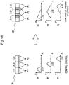
- the LCOS element of the switching element 25 is set to have pass bands that cause end portions of adjacent ones of the respective optical signals ⁇ 11 , ⁇ 22, and ⁇ 33 to overlap each other, as illustrated in the right drawing in Fig. 4B .
- the switching element 25 in the wavelength selective switch WSS of the present example embodiment performs switching so that end portions of adjacent ones of the respective optical signals ⁇ 11 , ⁇ 22, and ⁇ 33 overlap each other, as illustrated in the right drawing in Fig. 4B .
- the switching element 25 in the wavelength selective switch WSS performs the switching causing end portions of adjacent ones of the respective optical signals ⁇ 11 , ⁇ 22, and ⁇ 33 to overlap each other.
- the switching element 25 performs the switching so that the optical signal ⁇ 11 and a portion of the optical signal ⁇ 11 are outputted to the ports P1 and P2, respectively.
- the switching element 25 performs the switching so that a portion of the optical signal ⁇ 22, the optical signal ⁇ 22, another portion of the optical signal ⁇ 22 are outputted to the ports P1, P2, and P3, respectively. Still in addition, the switching element 25 performs the switching so that the optical signal ⁇ 33 and a portion of the optical signal ⁇ 33 are outputted to the ports P3 and P2, respectively.
- portions to which the switching element 25 applies the overlap control of optical signals are indicated by hatching.
- power P of the respective optical signals ⁇ 11 , ⁇ 22, and ⁇ 33 is illustrated in graphs in Fig. 4B .
- the control described above enables switching to be performed in such a way that end portions of adjacent ones of the optical signals ⁇ 11 , ⁇ 22, and ⁇ 33 overlap each other.
- a wavelength selective switch WSS with one input and N outputs (1 ⁇ N) was used was illustrated as an example, the present example embodiment may also be achieved using a wavelength selective switch WSS with N inputs and one output (N ⁇ 1).
- overlapping areas may be set among the pass bands of respective optical signals by adjusting the shapes of input and output waveguides of an AWG.
- overlapping areas may be set among the pass bands of respective optical signals by adjusting the shapes of a coupling portion between a slab waveguide and an input waveguide and a coupling portion between a slab waveguide and an output waveguide of an AWG.
- the invention according to the present example embodiment which has been described thus far, enables an optical device to be provided that is capable of suppressing an optical signal from being trimmed because of band narrowing due to optical filters.
- optical device 1 cyclic AWG
- the present invention is not limited to the example, and the number of input ports and the number of output ports of the optical device 1 may be determined arbitrarily.
- Fig. 5 is a diagram for a description of an optical device 2 according to the second example embodiment.
- the optical device 2 according to the present example embodiment is configured using a plurality of beam splitters BS_1 to BS_3 and a plurality of cyclic AWGs AWG_1 to AWG_3.
- the optical device 2 according to the present example embodiment may be used in an optical node, and more specifically an optical cross-connect node, in an optical communication network.
- the input sides of the beam splitters BS_1 to BS_3 are connected to three input side paths IN_#1 to IN_#3, respectively.
- Optical signals outputted from the beam splitters BS_1 to BS_3 are supplied to the cyclic AWGs AWG_1 to AWG_3, which are arranged at the succeeding stage of the beam splitters BS_1 to BS_3.
- Each of the beam splitters BS_1 to BS_3 is a beam splitter with one input and three outputs (1 ⁇ 3)
- each of the cyclic AWGs AWG_1 to AWG_3 is a cyclic AWG with three inputs and one output (3 ⁇ 1).
- the output ports of the cyclic AWGs AWG_1 to AWG_3 are connected to output side paths OUT_#1 to OUT_#3, respectively.
- Each of the beam splitters BS_1 to BS_3 outputs respective optical signals that are inputted to the beam splitter to an input port of each of the cyclic AWGs AWG_1 to AWG_3.
- the beam splitter BS_1 supplies optical signals Ch11, Ch12, and Ch13 supplied from the input side path IN_#1 to an input port P1 of the cyclic AWG AWG_1, an input port P2 of the cyclic AWG AWG_2, and an input port P3 of the cyclic AWG AWG_3.
- the beam splitter BS_2 supplies optical signals Ch21, Ch22, and Ch23 supplied from the input side path IN_#2 to an input port P2 of the cyclic AWG AWG_1, an input port P3 of the cyclic AWG AWG_2, and an input port P1 of the cyclic AWG AWG_3.
- the beam splitter BS_3 supplies optical signals Ch31, Ch32, and Ch33 supplied from the input side path IN_#3 to an input port P3 of the cyclic AWG AWG_1, an input port P1 of the cyclic AWG_2, and an input port P2 of the cyclic AWG_3.
- Each of the cyclic AWGs AWG_1 to AWG_3 filters respective optical signals inputted to each of the input ports P1 to P3 of the cyclic AWG and outputs the filtered optical signals to the output side path connected thereto.
- the cyclic AWG AWG_1 outputs the optical signals Ch11, Ch32, and Ch23 out of the optical signals inputted to the input ports P1 to P3 thereof to the output side path OUT_#1.
- the cyclic AWG AWG_2 outputs the optical signals Ch21, Ch12, and Ch33 out of the optical signals inputted to the input ports P1 to P3 thereof to the output side path OUT_#2.
- the cyclic AWG AWG_3 outputs the optical signals Ch31, Ch22, and Ch13 out of the optical signals inputted to the input ports P1 to P3 thereof to the output side path OUT_#3.
- the respective optical signals Ch11, Ch12, and Ch13, which pass through the input side path IN_#1 are optical signals in frequency bands different from one another.
- the optical signal Ch11 in the input side path IN_#1, the optical signal Ch21 in the input side path IN_#2, and the optical signal Ch31 in the input side path IN_#3 are optical signals in an identical frequency band.
- the optical signal Ch12 in the input side path IN_#1, the optical signal Ch22 in the input side path IN_#2, and the optical signal Ch32 in the input side path IN_#3 are optical signals in an identical frequency band.
- the optical signal Ch13 in the input side path IN_#1, the optical signal Ch23 in the input side path IN_#2, and the optical signal Ch33 in the input side path IN_#3 are optical signals in an identical frequency band. For this reason, in order to achieve WDM communication, these optical signals are required to be set not to be outputted to an identical output side path.
- the respective optical signals (Ch11, Ch12, Ch13, ..., and Ch33) are routed in channel units.
- the respective optical signals are constituted so that a plurality of wavelength-multiplexed signals can be allocated within the band of one channel.
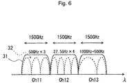
- Fig. 6 is a diagram for a description of channel bandwidths used by the optical device 2 according to the present example embodiment.
- a plurality of wavelength-multiplexed signals (optical signals) 32 can be allocated within one channel band 31.
- the bandwidths of the respective channels Ch11, Ch12, and Ch13 are set at 150 GHz and three optical signals with a bandwidth of 50 GHz are allocated in the channel Ch11 is illustrated as an example.
- four optical signals with a bandwidth of 37.5GHz are allocated in the channel Ch12 is illustrated.
- the pass-band width of each of the input ports P1 to P3 of each of the cyclic AWGs AWG_1 to AWG_3 (that is, the bandwidth of an optical filter) is set so as to correspond to the bandwidth of each of the channels (Ch11, Ch12, Ch13, ..., and Ch33).
- expansion of the pass-band width of each of the input ports P1 to P3 of each of the cyclic AWGs AWG_1 to AWG_3 to the bandwidth of a channel enables optical signals each having a predetermined bandwidth (that is, the channels Ch11, Ch12, Ch13, ... , and Ch33) to be respectively filtered.
- filtering the channel Ch11 in channel units enables three optical signals 32 each of which has a bandwidth of 50 GHz to be filtered in an identical direction.
- the optical signals Ch11, Ch12, and Ch13, Ch21, Ch22, and Ch23, and Ch31, Ch32, and Ch33 are supplied to the input ports P1, P2, and P3 of the cyclic AWG AWG_1, respectively.
- setting the pass-band width of each of the input ports P1 to P3 at 150 GHz enables an optical signal with a bandwidth per channel of 150 GHz to be passed.
- making the pass band and the center frequency of the input port P1 of the cyclic AWG AWG_1 coincide with the frequency band and the center frequency of the optical signal Ch11, respectively, enables only the optical signal Ch11 out of the optical signals Ch11, Ch12, and Ch13 supplied to the input port P1 to be passed. That is, making the pass band of the input port P1, that is, the pass band and the center frequency of an optical filter, coincide with the frequency band and the center frequency of the optical signal Ch11, respectively, enables the optical signals Ch12 and Ch13 to be removed.
- the pass-band width of each of the input ports P1 to P3 of each of the cyclic AWGs AWG_1 to AWG_3 may be set at m (m is a positive real number not less than 2) times of an adjacent frequency interval of a plurality of wavelength-multiplexed signals.
- m is a positive real number not less than 2
- the pass-band width of each of the input ports P1 to P3 is 150 GHz (see Ch12 in Fig. 6 ).
- communication with a capacity of 100 Gbps per optical signal it is possible to achieve communication with a capacity of 400 Gbps because four optical signals with a bandwidth of 37.5GHz can be allocated within one channel.
- the pass-band width of each of the input ports P1 to P3 is 150 GHz (see Ch11 in Fig. 6 ).
- the pass-band width of each of the input ports P1 to P3 is also 150 GHz.
- the optical device 2 is configured so that a plurality of wavelength-multiplexed signals can be allocated within the band of one channel.
- the number and the bandwidths of a plurality of wavelength-multiplexed signals allocated in the band of one channel may be set arbitrarily.
- the optical device 2 is configured so that a plurality of wavelength-multiplexed signals can be allocated within the band of one channel.
- the pass-band width of each of the input ports that is, the pass-band width of each of the optical filters corresponding to the respective input ports
- the cyclic AWG is expanded so that the cyclic AWG is able to filter optical signals in channel units. This configuration enables the number and the bandwidths of a plurality of wavelength-multiplexed signals allocated in each channel to be set arbitrarily, which enables optical signals that are to be transmitted to be set flexibly. That is, as illustrated in Fig.
- the number of optical signals allocated within one channel can be varied (see the channels Ch11 and Ch12) and optical signals with bandwidths different from each other can be allocated within one channel (see the channel Ch13). For this reason, optical signals that are to be transmitted may be set flexibly.
- the use of the cyclic AWGs AWG_1 to AWG_3 enables signals in an identical frequency band to be avoided from being outputted to an identical output side path.
- a plurality of wavelength-multiplexed signals are allocated within the band of one channel.
- setting the bandwidth 41 of the optical filter at 150 GHz enables optical signals to be transmitted with high density.
- each optical filter since the shape of each optical filter is not rectangular and there is individual variation in the center frequency and the bandwidth of each optical filter, the bandwidth of filters viewed at the receiving end becomes narrower (band narrowing) as the number of filters increases.
- Such a characteristic of filters causes optical signals to be trimmed at both ends of the frequency band thereof and to lose some signal components therein during a transmission process, and, eventually, signal errors increase at the receiving end, which disables reception of the signals.
- the bandwidth of the pass band 41 becomes narrower than the original bandwidth and comes to have a bandwidth indicated by a bandwidth 43.
- signals at both ends out of four optical signals 42 are trimmed (portions that are trimmed off are indicated by hatching)
- the level of the signals at both ends is decreased to a level at which the signals cannot be received.
- the respective optical filters are configured in such a way that portions of the pass bands of respective optical filters that respectively pass optical signals in channels adjacent to each other overlap each other.
- the optical device 2 is configured in such a way that a portion of the pass band of the optical filter of the port P1 and a portion of the pass band of the optical filter of the port P2 of the cyclic AWG AWG_1 illustrated in Fig. 5 overlap each other as pass bands 51_1 and 51_2 illustrated in Fig. 8 do. That is, an overlapping area 55 is set between the pass bands of the optical filters of the ports P1 and P2 of the cyclic AWG AWG_1.
- the pass band of the optical filter of the port P1 of the cyclic AWG AWG_1 corresponds to the wavelength band of the channel Ch11.
- the pass band of the optical filter of the port P2 of the cyclic AWG AWG_1 corresponds to the wavelength band of the channel Ch32.
- the pass band of each optical filter of the cyclic AWG may be made variable by, for example, adjusting the shapes of input and output waveguides of the cyclic AWG. Expanding pass bands corresponding to the respective optical filters enables pass bands to overlap each other between optical filters corresponding to adjacent ports.
- the pass band corresponding to each port of the cyclic AWG can be expanded by adjusting the shapes of a coupling portion between an input waveguide and a slab waveguide on the input side of the cyclic AWG and a coupling portion between a slab waveguide on the output side and an output waveguide of the cyclic AWG.
- the optical device 2 is configured in such a way that a portion of the pass band of the optical filter of the port P2 and a portion of the pass band of the optical filter of the port P3 of the cyclic AWG AWG_1 illustrated in Fig. 5 overlap each other as pass bands 51_2 and 51_3 illustrated in Fig. 8 do. That is, an overlapping area 56 is set between the pass bands of the optical filters of the ports P2 and P3 of the cyclic AWG AWG_1.
- the pass band of the optical filter of the port P2 of the cyclic AWG AWG_1 corresponds to the wavelength band of the channel Ch32.
- the pass band of the optical filter of the port P3 of the cyclic AWG AWG_1 corresponds to the wavelength band of the channel Ch23.
- the pass bands of the respective optical filters while maintaining a frequency interval between respective optical filters corresponding to channels adjacent to each other enables portions of the pass bands of respective optical filters corresponding to channels adjacent to each other to overlap each other.
- a frequency interval 54 between adjacent ones of the respective channels is maintained at 150 GHz
- the widths of the pass bands 51_1 to 51_3 of the respective optical filters corresponding to the respective channels are expanded from 150 GHz to 162.5GHz.
- the respective optical filters are configured in such a way that portions of the pass bands of respective optical filters that respectively pass optical signals in channels adjacent to each other overlap each other. Accordingly, optical signals may be suppressed from being trimmed at both ends of the frequency band thereof because of band narrowing on the optical signals during a transmission process of the optical signals and an optical signal that cannot be received may be suppressed from occurring. Therefore, transmission characteristics may be suppressed from deteriorating.
- the number of input side paths and the number of output side paths may be a number other than three. That is, in the case of a configuration including n input side paths IN_#1 to IN_#n and n output side paths OUT_#1 to OUT_#n, n beam splitters BS_1 to BS_n (each thereof is a beam splitter with one input and n outputs) that are connected to the input side paths IN_#1 to IN_#n, respectively, are arranged.
- n is a natural number not less than 2.
- n cyclic AWGs AWG_1 to AWG_n are arranged at the succeeding stage of the n beam splitters BS_1 to BS_n.
- Each of the n beam splitters BS_1 to BS_n outputs respective optical signals that are inputted to the beam splitter to an input port of each of the n cyclic AWGs AWG_1 to AWG_n.
- Each of the n cyclic AWGs AWG_1 to AWG_n filters respective optical signals inputted to each of the input ports of the cyclic AWG and outputs the filtered optical signals to the output side path connected thereto. This operation causes optical signals after routing to be outputted to the output side paths OUT_#1 to OUT_#n.
- the invention according to the present example embodiment which has been described thus far, enables an optical device to be provided that is capable of suppressing optical signals from being trimmed because of band narrowing due to optical filters.
- An optical device comprising a plurality of optical filters each of which filters an optical signal in a predetermined band out of a plurality of optical signals with wavelengths different from one another, wherein the plurality of optical filters are configured in such a way that portions of pass bands of respective optical filters that respectively pass optical signals with wavelengths adjacent to each other overlap each other.
- the optical device by expanding pass-band width of each of the plurality of optical filters while maintaining a frequency interval between optical filters adjacent to each other, making portions of pass bands of the respective optical filters adjacent to each other overlap each other.
- optical device wherein the plurality of optical filters are super-Gaussian type optical filters or optical filters each of which can be approximated with a super-Gaussian function.
- optical device according to any one of supplementary notes 1 to 3, wherein pass-band width per optical filter of the plurality of optical filter is a bandwidth that allows a plurality of optical signals to pass simultaneously.
- optical device a cyclic AWG that filters the respective optical signals, the respective optical signals are filtered in channel units, each of the channels is constituted so that a plurality of optical signals can be allocated within a band of the channel, and pass-band width per optical filter of the optical filters in the cyclic AWG corresponds to bandwidth of each of the channels.
- pass-band width per optical filter of the optical filters in the cyclic AWG is set at m (m is a positive real number not less than 2) times of an adjacent frequency interval of the plurality of optical signals.
- optical device wherein pass-band width of each of the optical filters in the cyclic AWG is 150 GHz, and a center frequency interval of the optical filters is 150 GHz.
- optical device wherein the adjacent frequency interval is 37.5GHz, and a value of the m is 4.
- optical device wherein the adjacent frequency interval is 50GHz, and a value of the m is 3.
- optical device wherein the adjacent frequency interval is 75GHz, and a value of the m is 2.
- optical device any one of supplementary notes 1 to 3, wherein the optical device is a wavelength selective switch that is capable of varying a pass band.
- optical device any one of supplementary notes 1 to 3, wherein the optical device is an AWG.
- a processing method of optical signals comprising:
- the processing method of optical signals according to supplementary note 13 comprising by expanding pass-band width of each of the plurality of optical filters while maintaining a frequency interval between the optical filters adjacent to each other, making portions of pass bands of the respective optical filters adjacent to each other overlap each other.
- pass-band width per optical filter of the plurality of optical filter is a bandwidth that allows a plurality of optical signals to pass simultaneously.
- each of the optical filters is set in such a way that pass-band width when the respective optical signals are filtered corresponds to bandwidth of a channel where a plurality of optical signals are allocated within a band of the channel and filters the respective optical signals in units of the channel.
Landscapes
- Physics & Mathematics (AREA)
- General Physics & Mathematics (AREA)
- Optics & Photonics (AREA)
- Engineering & Computer Science (AREA)
- Nonlinear Science (AREA)
- Computer Networks & Wireless Communication (AREA)
- Signal Processing (AREA)
- Electromagnetism (AREA)
- Microelectronics & Electronic Packaging (AREA)
- Optical Communication System (AREA)
- Optical Modulation, Optical Deflection, Nonlinear Optics, Optical Demodulation, Optical Logic Elements (AREA)
- Optical Integrated Circuits (AREA)
Applications Claiming Priority (2)
| Application Number | Priority Date | Filing Date | Title |
|---|---|---|---|
| JP2016038163 | 2016-02-29 | ||
| PCT/JP2017/006394 WO2017150278A1 (fr) | 2016-02-29 | 2017-02-21 | Dispositif optique |
Publications (2)
| Publication Number | Publication Date |
|---|---|
| EP3425434A1 true EP3425434A1 (fr) | 2019-01-09 |
| EP3425434A4 EP3425434A4 (fr) | 2019-10-30 |
Family
ID=59742805
Family Applications (1)
| Application Number | Title | Priority Date | Filing Date |
|---|---|---|---|
| EP17759744.0A Withdrawn EP3425434A4 (fr) | 2016-02-29 | 2017-02-21 | Dispositif optique |
Country Status (5)
| Country | Link |
|---|---|
| US (1) | US10539741B2 (fr) |
| EP (1) | EP3425434A4 (fr) |
| JP (1) | JP6763424B2 (fr) |
| CN (1) | CN109313309B (fr) |
| WO (1) | WO2017150278A1 (fr) |
Families Citing this family (7)
| Publication number | Priority date | Publication date | Assignee | Title |
|---|---|---|---|---|
| EP3425827B1 (fr) * | 2016-02-29 | 2021-01-20 | Nec Corporation | Dispositif de transmission optique |
| JP6988296B2 (ja) * | 2017-09-14 | 2022-01-05 | 富士通株式会社 | 伝送装置及び信号監視方法 |
| US10701465B2 (en) * | 2017-11-10 | 2020-06-30 | Huawei Technologies Co., Ltd. | Wide passband wavelength selective switch |
| CN109067472B (zh) * | 2018-08-23 | 2021-09-07 | 东南大学 | 一种基于重叠覆盖滤光片组的多色光信号接收方法 |
| EP3849114B1 (fr) | 2018-09-07 | 2024-04-10 | NEC Corporation | Dispositif de transmission optique, système de communication optique, et procédé de transmission de signal optique |
| JP7360024B2 (ja) * | 2019-08-30 | 2023-10-12 | 富士通株式会社 | ネットワークシステム |
| US12425753B2 (en) * | 2022-02-02 | 2025-09-23 | Infinera Corp. | Grouping of optical passbands for loading in an optical transmission spectrum using an affinity identifier |
Family Cites Families (18)
| Publication number | Priority date | Publication date | Assignee | Title |
|---|---|---|---|---|
| US5412744A (en) * | 1994-05-02 | 1995-05-02 | At&T Corp. | Frequency routing device having a wide and substantially flat passband |
| JPH09321701A (ja) * | 1996-05-31 | 1997-12-12 | Fujitsu Ltd | 光通信システム及び光増幅器 |
| EP0936483A3 (fr) * | 1998-02-10 | 1999-09-22 | Lucent Technologies Inc. | Routeur optique ayant des chemins de connections cohérents |
| EP1030480A3 (fr) | 1999-02-19 | 2002-06-12 | JDS Uniphase Inc. | Circuit optique configurable |
| JP4647074B2 (ja) * | 2000-10-04 | 2011-03-09 | 富士通株式会社 | 波長多重光通信システム |
| JP4622168B2 (ja) * | 2001-06-22 | 2011-02-02 | 住友電気工業株式会社 | 波長多重信号光監視装置、監視方法、及び光伝送システム |
| WO2003009508A1 (fr) * | 2001-07-19 | 2003-01-30 | Novx Systems Inc. | Commutateur optique a insertion-extraction |
| JP4540289B2 (ja) * | 2002-06-28 | 2010-09-08 | 富士通株式会社 | 波長多重光伝送システムおよび波長多重光伝送方法 |
| JP5691255B2 (ja) * | 2010-06-22 | 2015-04-01 | 富士通株式会社 | Osnr測定装置および光通信システム |
| JP5466657B2 (ja) | 2011-02-18 | 2014-04-09 | 日本電信電話株式会社 | 波長調整システム及び方法 |
| CN102695101B (zh) * | 2011-03-21 | 2015-11-18 | 苏州海光芯创光电科技有限公司 | 一种波分复用上的无源光网络 |
| US9160455B2 (en) * | 2011-07-14 | 2015-10-13 | Applied Optoelectronics, Inc. | External cavity laser array system and WDM optical system including same |
| GB201119922D0 (en) * | 2011-11-18 | 2012-01-04 | Cambridge Entpr Ltd | Optical signal transmission systems |
| JP5962455B2 (ja) * | 2012-11-21 | 2016-08-03 | 富士通株式会社 | 光伝送装置、ノード装置、光伝送方法および光伝送システム |
| US8983250B2 (en) * | 2013-03-14 | 2015-03-17 | Intelligent Fiber Optic Systems, Inc. | AWG filter for wavelength interrogator |
| JP6115364B2 (ja) | 2013-07-11 | 2017-04-19 | 富士通株式会社 | 光伝送装置、光伝送システム、及び光伝送方法 |
| JP6074859B2 (ja) * | 2013-09-19 | 2017-02-08 | 日本電信電話株式会社 | 光可変フィルタ |
| CN104092538B (zh) * | 2014-07-15 | 2017-04-12 | 华南师范大学 | 多用户波分复用qkd网络系统及其密钥分发与共享方法 |
-
2017
- 2017-02-21 CN CN201780013307.7A patent/CN109313309B/zh active Active
- 2017-02-21 JP JP2018503058A patent/JP6763424B2/ja active Active
- 2017-02-21 WO PCT/JP2017/006394 patent/WO2017150278A1/fr not_active Ceased
- 2017-02-21 US US16/078,980 patent/US10539741B2/en active Active
- 2017-02-21 EP EP17759744.0A patent/EP3425434A4/fr not_active Withdrawn
Also Published As
| Publication number | Publication date |
|---|---|
| JP6763424B2 (ja) | 2020-09-30 |
| CN109313309B (zh) | 2021-01-12 |
| CN109313309A (zh) | 2019-02-05 |
| JPWO2017150278A1 (ja) | 2018-12-06 |
| US10539741B2 (en) | 2020-01-21 |
| US20190064437A1 (en) | 2019-02-28 |
| WO2017150278A1 (fr) | 2017-09-08 |
| EP3425434A4 (fr) | 2019-10-30 |
Similar Documents
| Publication | Publication Date | Title |
|---|---|---|
| US10539741B2 (en) | Optical device with optical filters and processing method of optical signals | |
| US7088922B2 (en) | Wavelength division multiplexing optical communication system | |
| JP5176598B2 (ja) | 光分岐挿入装置および光伝送装置 | |
| US8903242B2 (en) | Directionless and colorless reconfigurable optical add/drop multiplexer | |
| US8315522B2 (en) | Wavelength routing system | |
| US8095011B2 (en) | Wavelength division multiplexing filter, wavelength division multiplexing system, and wavelength division multiplexing method | |
| JP4843659B2 (ja) | 光伝送ネットワークシステム、光伝送装置、及びそれらを用いた通過帯域割り当て方法 | |
| US6512864B1 (en) | Optical multiplexer/demultiplexer arrangement for WDM signals having in-band and out-of-band signal components | |
| US10097304B2 (en) | Optical switch, an optical switching apparatus, an optical communications network node and an optical communications network | |
| JP4152932B2 (ja) | 光分波方法および光合波方法、並びに、それを用いた光伝送装置 | |
| US10123100B2 (en) | Optical network | |
| KR100422372B1 (ko) | 채널 확장된 파장분할 다중기/역다중기 및 이를 이용한 파장 채널 선택기 | |
| CN110892656B (zh) | 光波长分离装置及光波长分离方法 | |
| EP3425827B1 (fr) | Dispositif de transmission optique | |
| JPWO2011162269A1 (ja) | 合分波器及び合分波方法 | |
| JP5772107B2 (ja) | 波長選択スイッチおよび光伝送装置 | |
| EP3091678B1 (fr) | Réseau de transmission optique à multiplexage en longueur d'onde | |
| CN104160645A (zh) | 利用融合信号添加和移除的多频带可重配置光学分插复用 | |
| US20120183292A1 (en) | Method and apparatus for trafficking wavelengths of different spacings within an optical node | |
| US20250105940A1 (en) | Partially Colored Flexgrid Wavelength-Division Multiplexer/Demultiplexer | |
| JP2011203539A (ja) | 波長変換システム及び波長変換方法 |
Legal Events
| Date | Code | Title | Description |
|---|---|---|---|
| STAA | Information on the status of an ep patent application or granted ep patent |
Free format text: STATUS: THE INTERNATIONAL PUBLICATION HAS BEEN MADE |
|
| PUAI | Public reference made under article 153(3) epc to a published international application that has entered the european phase |
Free format text: ORIGINAL CODE: 0009012 |
|
| STAA | Information on the status of an ep patent application or granted ep patent |
Free format text: STATUS: REQUEST FOR EXAMINATION WAS MADE |
|
| 17P | Request for examination filed |
Effective date: 20180924 |
|
| AK | Designated contracting states |
Kind code of ref document: A1 Designated state(s): AL AT BE BG CH CY CZ DE DK EE ES FI FR GB GR HR HU IE IS IT LI LT LU LV MC MK MT NL NO PL PT RO RS SE SI SK SM TR |
|
| AX | Request for extension of the european patent |
Extension state: BA ME |
|
| DAV | Request for validation of the european patent (deleted) | ||
| DAX | Request for extension of the european patent (deleted) | ||
| A4 | Supplementary search report drawn up and despatched |
Effective date: 20190930 |
|
| RIC1 | Information provided on ipc code assigned before grant |
Ipc: H04J 14/02 20060101ALI20190924BHEP Ipc: G02B 6/293 20060101ALI20190924BHEP Ipc: G02B 6/12 20060101AFI20190924BHEP |
|
| STAA | Information on the status of an ep patent application or granted ep patent |
Free format text: STATUS: THE APPLICATION HAS BEEN WITHDRAWN |
|
| 18W | Application withdrawn |
Effective date: 20191106 |