EP3428244B1 - Films de points quantiques utilisant des résines à phases multiples - Google Patents
Films de points quantiques utilisant des résines à phases multiples Download PDFInfo
- Publication number
- EP3428244B1 EP3428244B1 EP18186420.8A EP18186420A EP3428244B1 EP 3428244 B1 EP3428244 B1 EP 3428244B1 EP 18186420 A EP18186420 A EP 18186420A EP 3428244 B1 EP3428244 B1 EP 3428244B1
- Authority
- EP
- European Patent Office
- Prior art keywords
- phase
- acrylate
- resin
- film
- refractive index
- Prior art date
- Legal status (The legal status is an assumption and is not a legal conclusion. Google has not performed a legal analysis and makes no representation as to the accuracy of the status listed.)
- Active
Links
Images



Classifications
-
- C—CHEMISTRY; METALLURGY
- C09—DYES; PAINTS; POLISHES; NATURAL RESINS; ADHESIVES; COMPOSITIONS NOT OTHERWISE PROVIDED FOR; APPLICATIONS OF MATERIALS NOT OTHERWISE PROVIDED FOR
- C09K—MATERIALS FOR MISCELLANEOUS APPLICATIONS, NOT PROVIDED FOR ELSEWHERE
- C09K11/00—Luminescent materials, e.g. electroluminescent or chemiluminescent
- C09K11/02—Use of particular materials as binders, particle coatings or suspension media therefor
-
- B—PERFORMING OPERATIONS; TRANSPORTING
- B32—LAYERED PRODUCTS
- B32B—LAYERED PRODUCTS, i.e. PRODUCTS BUILT-UP OF STRATA OF FLAT OR NON-FLAT, e.g. CELLULAR OR HONEYCOMB, FORM
- B32B37/00—Methods or apparatus for laminating, e.g. by curing or by ultrasonic bonding
- B32B37/14—Methods or apparatus for laminating, e.g. by curing or by ultrasonic bonding characterised by the properties of the layers
- B32B37/24—Methods or apparatus for laminating, e.g. by curing or by ultrasonic bonding characterised by the properties of the layers with at least one layer not being coherent before laminating, e.g. made up from granular material sprinkled onto a substrate
-
- C—CHEMISTRY; METALLURGY
- C08—ORGANIC MACROMOLECULAR COMPOUNDS; THEIR PREPARATION OR CHEMICAL WORKING-UP; COMPOSITIONS BASED THEREON
- C08J—WORKING-UP; GENERAL PROCESSES OF COMPOUNDING; AFTER-TREATMENT NOT COVERED BY SUBCLASSES C08B, C08C, C08F, C08G or C08H
- C08J3/00—Processes of treating or compounding macromolecular substances
- C08J3/24—Crosslinking, e.g. vulcanising, of macromolecules
- C08J3/241—Preventing premature crosslinking by physical separation of components, e.g. encapsulation
-
- C—CHEMISTRY; METALLURGY
- C08—ORGANIC MACROMOLECULAR COMPOUNDS; THEIR PREPARATION OR CHEMICAL WORKING-UP; COMPOSITIONS BASED THEREON
- C08J—WORKING-UP; GENERAL PROCESSES OF COMPOUNDING; AFTER-TREATMENT NOT COVERED BY SUBCLASSES C08B, C08C, C08F, C08G or C08H
- C08J5/00—Manufacture of articles or shaped materials containing macromolecular substances
- C08J5/20—Manufacture of shaped structures of ion-exchange resins
- C08J5/22—Films, membranes or diaphragms
-
- C—CHEMISTRY; METALLURGY
- C08—ORGANIC MACROMOLECULAR COMPOUNDS; THEIR PREPARATION OR CHEMICAL WORKING-UP; COMPOSITIONS BASED THEREON
- C08L—COMPOSITIONS OF MACROMOLECULAR COMPOUNDS
- C08L33/00—Compositions of homopolymers or copolymers of compounds having one or more unsaturated aliphatic radicals, each having only one carbon-to-carbon double bond, and only one being terminated by only one carboxyl radical, or of salts, anhydrides, esters, amides, imides or nitriles thereof; Compositions of derivatives of such polymers
- C08L33/04—Homopolymers or copolymers of esters
- C08L33/06—Homopolymers or copolymers of esters of esters containing only carbon, hydrogen and oxygen, which oxygen atoms are present only as part of the carboxyl radical
- C08L33/08—Homopolymers or copolymers of acrylic acid esters
-
- C—CHEMISTRY; METALLURGY
- C08—ORGANIC MACROMOLECULAR COMPOUNDS; THEIR PREPARATION OR CHEMICAL WORKING-UP; COMPOSITIONS BASED THEREON
- C08L—COMPOSITIONS OF MACROMOLECULAR COMPOUNDS
- C08L63/00—Compositions of epoxy resins; Compositions of derivatives of epoxy resins
-
- C—CHEMISTRY; METALLURGY
- C09—DYES; PAINTS; POLISHES; NATURAL RESINS; ADHESIVES; COMPOSITIONS NOT OTHERWISE PROVIDED FOR; APPLICATIONS OF MATERIALS NOT OTHERWISE PROVIDED FOR
- C09K—MATERIALS FOR MISCELLANEOUS APPLICATIONS, NOT PROVIDED FOR ELSEWHERE
- C09K11/00—Luminescent materials, e.g. electroluminescent or chemiluminescent
- C09K11/08—Luminescent materials, e.g. electroluminescent or chemiluminescent containing inorganic luminescent materials
- C09K11/70—Luminescent materials, e.g. electroluminescent or chemiluminescent containing inorganic luminescent materials containing phosphorus
-
- C—CHEMISTRY; METALLURGY
- C09—DYES; PAINTS; POLISHES; NATURAL RESINS; ADHESIVES; COMPOSITIONS NOT OTHERWISE PROVIDED FOR; APPLICATIONS OF MATERIALS NOT OTHERWISE PROVIDED FOR
- C09K—MATERIALS FOR MISCELLANEOUS APPLICATIONS, NOT PROVIDED FOR ELSEWHERE
- C09K11/00—Luminescent materials, e.g. electroluminescent or chemiluminescent
- C09K11/08—Luminescent materials, e.g. electroluminescent or chemiluminescent containing inorganic luminescent materials
- C09K11/70—Luminescent materials, e.g. electroluminescent or chemiluminescent containing inorganic luminescent materials containing phosphorus
- C09K11/701—Chalcogenides
- C09K11/703—Chalcogenides with zinc or cadmium
-
- H—ELECTRICITY
- H10—SEMICONDUCTOR DEVICES; ELECTRIC SOLID-STATE DEVICES NOT OTHERWISE PROVIDED FOR
- H10H—INORGANIC LIGHT-EMITTING SEMICONDUCTOR DEVICES HAVING POTENTIAL BARRIERS
- H10H20/00—Individual inorganic light-emitting semiconductor devices having potential barriers, e.g. light-emitting diodes [LED]
- H10H20/80—Constructional details
- H10H20/81—Bodies
- H10H20/811—Bodies having quantum effect structures or superlattices, e.g. tunnel junctions
-
- H—ELECTRICITY
- H10—SEMICONDUCTOR DEVICES; ELECTRIC SOLID-STATE DEVICES NOT OTHERWISE PROVIDED FOR
- H10H—INORGANIC LIGHT-EMITTING SEMICONDUCTOR DEVICES HAVING POTENTIAL BARRIERS
- H10H20/00—Individual inorganic light-emitting semiconductor devices having potential barriers, e.g. light-emitting diodes [LED]
- H10H20/80—Constructional details
- H10H20/85—Packages
- H10H20/851—Wavelength conversion means
- H10H20/8511—Wavelength conversion means characterised by their material, e.g. binder
- H10H20/8512—Wavelength conversion materials
-
- H—ELECTRICITY
- H10—SEMICONDUCTOR DEVICES; ELECTRIC SOLID-STATE DEVICES NOT OTHERWISE PROVIDED FOR
- H10H—INORGANIC LIGHT-EMITTING SEMICONDUCTOR DEVICES HAVING POTENTIAL BARRIERS
- H10H20/00—Individual inorganic light-emitting semiconductor devices having potential barriers, e.g. light-emitting diodes [LED]
- H10H20/80—Constructional details
- H10H20/85—Packages
- H10H20/851—Wavelength conversion means
- H10H20/8511—Wavelength conversion means characterised by their material, e.g. binder
- H10H20/8512—Wavelength conversion materials
- H10H20/8513—Wavelength conversion materials having two or more wavelength conversion materials
-
- B—PERFORMING OPERATIONS; TRANSPORTING
- B32—LAYERED PRODUCTS
- B32B—LAYERED PRODUCTS, i.e. PRODUCTS BUILT-UP OF STRATA OF FLAT OR NON-FLAT, e.g. CELLULAR OR HONEYCOMB, FORM
- B32B37/00—Methods or apparatus for laminating, e.g. by curing or by ultrasonic bonding
- B32B37/14—Methods or apparatus for laminating, e.g. by curing or by ultrasonic bonding characterised by the properties of the layers
- B32B37/24—Methods or apparatus for laminating, e.g. by curing or by ultrasonic bonding characterised by the properties of the layers with at least one layer not being coherent before laminating, e.g. made up from granular material sprinkled onto a substrate
- B32B2037/243—Coating
-
- B—PERFORMING OPERATIONS; TRANSPORTING
- B32—LAYERED PRODUCTS
- B32B—LAYERED PRODUCTS, i.e. PRODUCTS BUILT-UP OF STRATA OF FLAT OR NON-FLAT, e.g. CELLULAR OR HONEYCOMB, FORM
- B32B2307/00—Properties of the layers or laminate
- B32B2307/40—Properties of the layers or laminate having particular optical properties
- B32B2307/418—Refractive
-
- B—PERFORMING OPERATIONS; TRANSPORTING
- B32—LAYERED PRODUCTS
- B32B—LAYERED PRODUCTS, i.e. PRODUCTS BUILT-UP OF STRATA OF FLAT OR NON-FLAT, e.g. CELLULAR OR HONEYCOMB, FORM
- B32B2307/00—Properties of the layers or laminate
- B32B2307/70—Other properties
- B32B2307/724—Permeability to gases, adsorption
- B32B2307/7242—Non-permeable
-
- B—PERFORMING OPERATIONS; TRANSPORTING
- B82—NANOTECHNOLOGY
- B82Y—SPECIFIC USES OR APPLICATIONS OF NANOSTRUCTURES; MEASUREMENT OR ANALYSIS OF NANOSTRUCTURES; MANUFACTURE OR TREATMENT OF NANOSTRUCTURES
- B82Y20/00—Nanooptics, e.g. quantum optics or photonic crystals
-
- Y—GENERAL TAGGING OF NEW TECHNOLOGICAL DEVELOPMENTS; GENERAL TAGGING OF CROSS-SECTIONAL TECHNOLOGIES SPANNING OVER SEVERAL SECTIONS OF THE IPC; TECHNICAL SUBJECTS COVERED BY FORMER USPC CROSS-REFERENCE ART COLLECTIONS [XRACs] AND DIGESTS
- Y10—TECHNICAL SUBJECTS COVERED BY FORMER USPC
- Y10T—TECHNICAL SUBJECTS COVERED BY FORMER US CLASSIFICATION
- Y10T156/00—Adhesive bonding and miscellaneous chemical manufacture
- Y10T156/10—Methods of surface bonding and/or assembly therefor
Definitions
- LEDs Light-emitting diodes
- LCD liquid crystal display
- LED devices are typically made from inorganic solid-state semiconductor materials. The material used to make the LED determines the color of light produced by the LED. Each material emits light with a particular wavelength spectrum, i.e., light having a particular mix of colors. Common materials include AlGaAs (red), AlGaInP (orange-yellow-green), and AlGaInN (green-blue).
- LEDs that produce white light which is a mixture of fundamental colors (e.g., red, green and blue) or that produce light not available using the usual LED semiconductor materials are needed for many applications.
- the most usual method of color mixing to produce a required color, such as white is to use a combination of phosphorescent materials that are placed on top of the solid-state LED whereby the light from the LED (the "primary light”) is absorbed by the phosphorescent material and then re-emitted at a different frequency (the “secondary light”).
- the phosphorescent material "down converts" a portion of the primary light.
- the most common phosphor materials are solid-state semiconductor materials, such as trivalent rare-earth doped oxides or halophosphates.
- White emission can be obtained by blending a blue light-emitting LED with a green phosphor such as, SrGa 2 S 4 :Eu 2 2+ and a red phosphor such as, SrSi 5 Ni 8 :Eu 2 2+ or a UV light-emitting LED plus a yellow phosphor such as, Sr 2 P 2 O 7 :Eu 2+ ; Mu 2+ , and a blue-green phosphor.
- White LEDs can also be made by combining a blue LED with a yellow phosphor.
- US 2010/123155 A1 discloses a formulation for use in the fabrication of a light-emitting device, the formulation including a population of semiconductor nanoparticles incorporated into a plurality of discrete microbeads comprising an optically transparent medium, the nanoparticle-containing medium being embedded in a host light-emitting diode encapsulation medium.
- a method of preparing such a formulation is also described, as is a light-emitting device including a primary light source in optical communication with such a formulation and a method of fabricating the same.
- Films containing QDs are described herein.
- the films may be used as components for LED lighting devices, particularly, as phosphor films for down-converting light emitted from a solid-state LED semiconductor material.
- a film comprising a first phase comprising an acrylate and quantum dots, and a second phase comprising an epoxy or polyurethane, wherein regions of the first phase are dispersed throughout the second phase, and the film is a cured emulsion
- a panel comprising a film according to the first aspect of the invention disposed between two gas barrier sheets.
- the acrylate may be lauryl methacrylate and/or the epoxy may be bisphenol A diglycidyl or glycidyl methacrylate.
- the refractive index of the acrylate and the refractive index of the epoxy or the polyurethane differ by less than 5 %, optionally wherein the refractive index of the acrylate and the refractive index of the epoxy or the polyurethane differ by less than 1 %.
- the first phase may comprise one or more of: a photoinitiator, a cross-linking agent, a polymerization catalyst, a refractive index modifier, a filler, a scattering agent, a viscosity modifier, a surfactant or an emulsifying agent.
- the second phase may comprise one or more of a photoinitiator, a cross-linking agent, a polymerization catalyst, a surfactant or an emulsifying agent.
- a method of fabricating a panel according to the second aspect of the invention comprises the steps of suspending quantum dots in a solution of an acrylate resin; adding the quantum dot suspension to a solution of an epoxy resin or a polyurethane resin to yield an emulsion; laminating the emulsion between gas barrier films to form a film of the emulsion; and curing the laminated emulsion film.
- the acrylate may be lauryl methacrylate and/or the epoxy may be bisphenol A diglycidyl or glycidyl methacrylate.
- the first is the large surface-to-volume ratio. As particles become smaller, the ratio of the number of surface atoms to those in the interior increases. This leads to the surface properties playing an important role in the overall properties of the material.
- the second factor is a change in the electronic properties of the material when the material is very small in size. At extremely small sizes quantum confinement causes the material's band gap to gradually increase as the size of the particles decrease. This effect is a consequence of the confinement of an ' electron in a box' giving rise to discrete energy levels similar to those observed in atoms and molecule rather than a continuous band as observed in the corresponding bulk semiconductor material.
- the "electron and hole" produced by the absorption of electromagnetic radiation are closer together than they would be in the corresponding macrocrystalline material. This leads to a narrow bandwidth emission that depends upon the particle size and composition of the nanoparticle material. QDs therefore have higher kinetic energy than the corresponding macrocrystalline material and consequently the first excitonic transition (band gap) increases in energy with decreasing particle diameter.
- QD nanoparticles of a single semiconductor material tend to have relatively low quantum efficiencies due to electron-hole recombination occurring at defects and dangling bonds situated on the nanoparticle surface, which may lead to non-radiative electron-hole recombinations.
- One method to eliminate such defects and dangling bonds on the inorganic surface of the QD is to grow a second inorganic material, having a wider band-gap and small lattice mismatch to that of the core material, epitaxially on the surface of the core particle, producing a "core-shell" particle.
- Core-shell particles separate any carriers confined in the core from surface states that would otherwise act as non-radiative recombination centers.
- the QDs are preferably incorporated into the LED encapsulating material while remaining as fully mono-dispersed as possible and without significant loss of quantum efficiency.
- the methods developed to date are problematic, not least because of the nature of current LED encapsulants. QDs can agglomerate when formulated into current LED encapsulants, thereby reducing the optical performance of the QDs.
- oxygen can migrate through the encapsulant to the surfaces of the QDs, which can lead to photo-oxidation and, as a result, a drop in quantum yield (QY).
- Figure 1 illustrates a prior art embodiment 100, wherein a QD-containing film 101 is disposed on a transparent substrate 102.
- a QD-containing film 101 is disposed on a transparent substrate 102.
- Such a film can be useful, for example, to down-convert primary light 103 from a primary light source 104 by absorbing primary light 103 and emitting secondary light 105.
- a portion 106 of primary light may also be transmitted through the film and substrate so that the total light emanating from the film and substrate is a mixture of the primary and secondary light.
- QD-containing films such as film 101 in Figure 1
- Multi-phase films utilizing at least a first phase (phase 1) resin that is compatible with the QD material and at least a second phase (phase 2) resin that is efficient at rejecting O 2 are described herein.
- Figure 3 illustrate a plan view of such a film 300, wherein QDs 301 are dispersed in a first polymer phase 302, which is typically a hydrophobic material such as an acrylate resin. Regions of the first polymer phase are dispersed throughout a second polymer phase 303, which is typically an oxygen-impermeable material such as epoxy.
- the multi-phase films described herein overcome many of the problems described above.
- the phase 1 resin is compatible with the QDs and therefore allows a high initial QY.
- the phase 2 resin is impermeable to oxygen, and therefore protects the QDs from oxidation without the need to seal the edges of the panel.
- the term "film” includes, not only 2-dimensional (i.e. flat) sheets, as illustrated in Figures 1-3 , but can also include 3-dimensional shapes.
- FIG 4 is a flowchart illustrating steps of a method of preparing multi-phase films as described herein.
- the QDs are dispersed in a solution of the phase 1 resin (or resin monomer) 401.
- the phase 1 resin is an acrylate resin.
- phase 1 resins include, poly(methyl (meth)acrylate), poly(ethyl (meth)acrylate), poly(n-propyl (meth)acrylate), poly(butyl (meth)acrylate), poly(n-pentyl (meth)acrylate), poly(n-hexyl (meth)acrylate), poly(cyclohexyl (meth)acrylate), poly(2-ethyl hexyl (meth)acrylate), poly(octyl (meth)acrylate), poly(isooctyl (meth)acrylate), poly(n-decyl (meth)acrylate), poly(isodecyl (meth)acrylate), poly(lauryl(meth)acrylate), poly(hexadecyl (meth)acrylate), poly(octadecyl (meth)acrylate), poly(isobornyl (meth)acrylate), poly(isobutylene), polystyrene
- the phase 1 resin can be any resin that is compatible with the QDs.
- the phase 1 resin may or may not be cross-linked or cross-linkable.
- the phase 1 resin may be a curable resin, for example, curable using UV light.
- the solution of 401 may further include one or more of a photoinitiator, a cross-linking agent, a polymerization catalyst, a refractive index modifier (either inorganic one such as ZnS nanoparticles or organic one such as high refractive index monomers or poly(propylene sulfide)), a filler such as fumed silica, a scattering agent such as barium sulfate, a viscosity modifier, a surfactant or emulsifying agent, or the like.
- a photoinitiator either inorganic one such as ZnS nanoparticles or organic one such as high refractive index monomers or poly(propylene sulfide)
- a filler such as
- the QD-phase 1 resin dispersion can then be mixed with a solution of the phase 2 resin (or resin monomer) 402.
- the phase 2 resin is a better oxygen barrier than the phase 1 resin.
- the phase 2 resin is generally a hydrophilic resin.
- the phase 2 resin may or may not be cross-linkable.
- the phase 2 resin may be a curable resin, for example, curable using UV light. Examples of phase 2 resins include epoxy-based resins and polyurethanes-based resins.
- the solution of phase 2 resin may also include one or more of a photoinitiator, a cross-linking agent, a polymerization catalyst, a surfactant or emulsifying agent, or the like.
- the phase 1 - phase 2 mixture forms an emulsion 403, typically and emulsion of phase 1 resin suspended in phase 2 resin.
- the emulsion composition can be adjusted by adjusting the relative concentrations of phase 1 and phase 2 resins, the rate of stirring of the mixture, the relative hydrophobicity of the resins, and the like.
- One or more emulsifying agents, surfactants, or other compounds useful for supporting stable emulsions may be used.
- Comparative Example 1A Green InP/ZnS QDs (120 Optical Density (OD)) were prepared as described in U.S. Patent Application No. 13/624,632, filed September 23, 2011 .
- the QDs were added to a degassed vial, the toluene evaporated, and the resultant solid QD re-dispersed in degassed lauryl methacrylate (LMA, 2.64mL) containing IRG819/IRG651 (Igracure®) photoinitiators (9/18mg).
- LMA degassed lauryl methacrylate
- IRG819/IRG651 Igracure® photoinitiators
- Example 3 Green InP/ZnS QDs (120 Optical Density (OD)) were prepared as described in U.S. Patent Application No. 13/624,632, filed September 23, 2011 .
- the QDs were re-dispersed in degassed lauryl methacrylate (LMA, 1.2 mL) by stirring under nitrogen overnight.
- IRG819 photoinitiator (3 mg) was dissolved in 0.6 mL of the QD dispersion in LMA.
- TMPTM crosslinker (0.073mL) was then added. The mixture was further stirred for 30 min under nitrogen, affording phase 1 resin with QD concentration at 89.2 OD/mL.
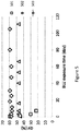
- Diamond-shaped data points 502 represent the QY of a two-phase film of LMA/epoxy resin containing QDs prepared as describe in Example 1b above.
- the initial QY of the LMA/epoxy two-phase film is also about 60 %, but unlike that of the single-phase film, the QY of the two-phase film remains constant over the time period of the experiment.
- the stability of the QY indicates that the two-phase film effectively prevents oxidation of the QDs.
Landscapes
- Chemical & Material Sciences (AREA)
- Organic Chemistry (AREA)
- Engineering & Computer Science (AREA)
- Materials Engineering (AREA)
- Health & Medical Sciences (AREA)
- Chemical Kinetics & Catalysis (AREA)
- Medicinal Chemistry (AREA)
- Polymers & Plastics (AREA)
- Inorganic Chemistry (AREA)
- Manufacturing & Machinery (AREA)
- Analytical Chemistry (AREA)
- Led Device Packages (AREA)
- Manufacture Of Macromolecular Shaped Articles (AREA)
- Compositions Of Macromolecular Compounds (AREA)
- Optical Filters (AREA)
- Luminescent Compositions (AREA)
- Processes Of Treating Macromolecular Substances (AREA)
Claims (13)
- Film comprenant :une première phase comprenant un acrylate et des points quantiques ; etune seconde phase comprenant un époxy ou un polyuréthane ;dans lequel des régions de la première phase sont dispersées au sein de la seconde phase, et le film est une émulsion durcie.
- Panneau comprenant un film selon la revendication 1 qui est disposé entre deux feuilles barrières aux gaz.
- Panneau selon la revendication 2, dans lequel l'acrylate est le méthacrylate de lauryle et/ou l'époxy est l'éther de diglycidyle ou le méthacrylate de glycidyle de bisphénol A.
- Panneau selon la revendication 2 ou la revendication 3, dans lequel l'indice de réfraction de l'acrylate et l'indice de réfraction de l'époxy ou du polyuréthane diffèrent de moins de 5 %, facultativement dans lequel l'indice de réfraction de l'acrylate et l'indice de réfraction de l'époxy ou du polyuréthane diffèrent de moins de 1 %.
- Panneau selon l'une quelconque des revendications 2 à 4, dans lequel la première phase comprend un ou plusieurs parmi : un photo-initiateur, un agent de réticulation, un catalyseur de polymérisation, un agent de modification d'indice de réfraction, un agent de remplissage, un agent de diffusion, un agent de modification de viscosité, un agent tensioactif et un agent émulsifiant.
- Panneau selon l'une quelconque des revendications 2 à 5, dans lequel la seconde phase comprend un ou plusieurs parmi un photo-initiateur, un agent de réticulation, un catalyseur de polymérisation, un agent tensioactif et un agent émulsifiant.
- Procédé de fabrication d'un panneau selon l'une quelconque des revendications 2 à 6, dans lequel le procédé comprend les étapes constituées par :la suspension de points quantiques dans une solution d'une résine acrylate ;l'ajout de la suspension de points quantiques à une solution d'une résine époxy ou d'une résine polyuréthane pour obtenir une émulsion ;le laminage de l'émulsion entre des films barrières aux gaz pour former un film de l'émulsion ; etle durcissement du film d'émulsion laminé.
- Procédé de fabrication d'un panneau selon la revendication 7, dans lequel l'acrylate est le méthacrylate de lauryle et/ou l'époxy est l'éther de diglycidyle ou le méthacrylate de glycidyle de bisphénol A.
- Procédé de fabrication d'un panneau selon la revendication 7 ou la revendication 8, dans lequel l'indice de réfraction de l'acrylate et l'indice de réfraction de l'époxy ou du polyuréthane diffèrent de moins de 5 %, facultativement dans lequel l'indice de réfraction de l'acrylate et l'indice de réfraction de l'époxy ou du polyuréthane diffèrent de moins de 1 %.
- Procédé de fabrication d'un panneau selon l'une quelconque des revendications 7 à 9, dans lequel la première phase comprend un ou plusieurs parmi : un photo-initiateur, un agent de réticulation, un catalyseur de polymérisation, un agent de modification d'indice de réfraction, un agent de remplissage, un agent de diffusion, un agent de modification de viscosité, un agent tensioactif et un agent émulsifiant.
- Procédé de fabrication d'un panneau selon l'une quelconque des revendications 7 à 10, dans lequel la seconde phase comprend un ou plusieurs parmi un photo-initiateur, un agent de réticulation, un catalyseur de polymérisation, un agent tensioactif et un agent émulsifiant.
- Dispositif électroluminescent comprenant un matériau semiconducteur de LED à l'état solide en communication optique avec un panneau selon l'une quelconque des revendications 2 à 6.
- Procédé de préparation d'un film, le procédé comprenant :la suspension de points quantiques dans une solution d'une résine acrylate ;l'ajout de la suspension de points quantiques à une solution d'une résine époxy ou d'une résine polyuréthane pour obtenir une émulsion ;la formation d'un film de l'émulsion ; etle durcissement du film d'émulsion.
Applications Claiming Priority (3)
| Application Number | Priority Date | Filing Date | Title |
|---|---|---|---|
| US201361865692P | 2013-08-14 | 2013-08-14 | |
| EP14753301.2A EP3033404B1 (fr) | 2013-08-14 | 2014-08-13 | Films de points quantiques utilisant des résines à phases multiples |
| PCT/GB2014/052471 WO2015022526A1 (fr) | 2013-08-14 | 2014-08-13 | Films de points quantiques utilisant des résines à phases multiples |
Related Parent Applications (2)
| Application Number | Title | Priority Date | Filing Date |
|---|---|---|---|
| EP14753301.2A Division EP3033404B1 (fr) | 2013-08-14 | 2014-08-13 | Films de points quantiques utilisant des résines à phases multiples |
| EP14753301.2A Division-Into EP3033404B1 (fr) | 2013-08-14 | 2014-08-13 | Films de points quantiques utilisant des résines à phases multiples |
Publications (2)
| Publication Number | Publication Date |
|---|---|
| EP3428244A1 EP3428244A1 (fr) | 2019-01-16 |
| EP3428244B1 true EP3428244B1 (fr) | 2021-07-28 |
Family
ID=51390133
Family Applications (2)
| Application Number | Title | Priority Date | Filing Date |
|---|---|---|---|
| EP18186420.8A Active EP3428244B1 (fr) | 2013-08-14 | 2014-08-13 | Films de points quantiques utilisant des résines à phases multiples |
| EP14753301.2A Active EP3033404B1 (fr) | 2013-08-14 | 2014-08-13 | Films de points quantiques utilisant des résines à phases multiples |
Family Applications After (1)
| Application Number | Title | Priority Date | Filing Date |
|---|---|---|---|
| EP14753301.2A Active EP3033404B1 (fr) | 2013-08-14 | 2014-08-13 | Films de points quantiques utilisant des résines à phases multiples |
Country Status (8)
| Country | Link |
|---|---|
| US (4) | US9680068B2 (fr) |
| EP (2) | EP3428244B1 (fr) |
| JP (2) | JP6475722B2 (fr) |
| KR (5) | KR101954160B1 (fr) |
| CN (2) | CN109456753B (fr) |
| HK (1) | HK1219290A1 (fr) |
| TW (2) | TWI606252B (fr) |
| WO (1) | WO2015022526A1 (fr) |
Families Citing this family (51)
| Publication number | Priority date | Publication date | Assignee | Title |
|---|---|---|---|---|
| EP3428244B1 (fr) * | 2013-08-14 | 2021-07-28 | Nanoco Technologies, Ltd. | Films de points quantiques utilisant des résines à phases multiples |
| US9574135B2 (en) * | 2013-08-22 | 2017-02-21 | Nanoco Technologies Ltd. | Gas phase enhancement of emission color quality in solid state LEDs |
| US9708532B2 (en) * | 2014-03-28 | 2017-07-18 | Nanoco Technologies Ltd. | Quantum dot compositions |
| CN106536676B (zh) * | 2014-08-14 | 2019-08-16 | 株式会社Lg化学 | 发光膜 |
| KR102353095B1 (ko) | 2014-12-26 | 2022-01-19 | 엔에스 마테리얼스 아이엔씨. | 파장 변환 부재 및 그 제조 방법 |
| KR102052101B1 (ko) * | 2015-02-25 | 2019-12-04 | 동우 화인켐 주식회사 | 자발광 감광성 수지 조성물, 이를 이용하여 제조된 컬러필터 및 화상표시장치 |
| CN107406602B (zh) * | 2015-03-12 | 2020-12-22 | 株式会社Lg化学 | 用于光学膜的组合物和包含其的光学膜 |
| KR101756522B1 (ko) * | 2015-03-16 | 2017-07-10 | 엘지전자 주식회사 | 양자점-수지 복합체의 제조 방법, 양자점-수지 복합체, 이를 포함하는 광 변환 필름, 백라이트 유닛 및 표시장치 |
| EP3070109B1 (fr) * | 2015-03-16 | 2018-12-05 | Rohm and Haas Electronic Materials LLC | Composite de polymère multicouche pour encapsuler des points quantiques |
| KR102028439B1 (ko) * | 2015-03-19 | 2019-10-04 | 동우 화인켐 주식회사 | 자발광 감광성 수지 조성물, 이를 포함하는 컬러필터 및 화상표시장치 |
| KR101686736B1 (ko) | 2015-04-17 | 2016-12-14 | 엘지전자 주식회사 | 양자점-고분자 복합체의 제조 방법, 양자점-고분자 복합체, 이를 포함하는 광 변환 필름, 백라이트 유닛 및 표시장치 |
| JP6627305B2 (ja) * | 2015-07-23 | 2020-01-08 | 凸版印刷株式会社 | ガスバリアフィルム及び色変換部材。 |
| KR101959461B1 (ko) * | 2015-07-29 | 2019-03-18 | 주식회사 엘지화학 | 광학 필름 |
| KR102010812B1 (ko) * | 2015-09-23 | 2019-08-14 | 주식회사 엘지화학 | 광학 부재 및 이를 포함하는 디스플레이 장치 |
| US20170125650A1 (en) | 2015-11-02 | 2017-05-04 | Nanoco Technologies Ltd. | Display devices comprising green-emitting quantum dots and red KSF phosphor |
| DE102015014526A1 (de) * | 2015-11-11 | 2017-05-11 | Giesecke & Devrient Gmbh | Sicherheitspigment, lumineszierendes Polymerharz und Verfahren zum Herstellen desselben |
| KR101985804B1 (ko) * | 2015-11-20 | 2019-06-04 | 주식회사 엘지화학 | 광학 부재용 조성물 |
| KR102574271B1 (ko) * | 2015-12-23 | 2023-09-05 | 아반타마 아게 | 디스플레이 장치 |
| EP3184602B1 (fr) | 2015-12-23 | 2018-07-04 | Avantama AG | Composant luminescent |
| US10655815B2 (en) | 2016-01-22 | 2020-05-19 | Nanoco Technologies Ltd. | Quantum dot-based lighting devices for animal husbandry and aquariums |
| KR102006378B1 (ko) * | 2016-02-04 | 2019-08-01 | 주식회사 엘지화학 | 광학 필름용 조성물 및 이를 포함하는 광학 필름 |
| CN108603105A (zh) * | 2016-02-12 | 2018-09-28 | 纳米技术有限公司 | 高度稳定的含量子点聚合物膜 |
| US10765885B2 (en) * | 2016-02-26 | 2020-09-08 | Nanoco Technologies Ltd. | Phototherapy mask with quantum dot phosphors |
| CN105870346B (zh) * | 2016-04-15 | 2018-07-03 | 深圳市华星光电技术有限公司 | Led显示屏的制造方法和led显示屏 |
| TWI641645B (zh) * | 2016-07-08 | 2018-11-21 | 羅門哈斯電子材料有限公司 | 用於囊封量子點之多層聚合物複合物 |
| US10787231B2 (en) * | 2016-07-29 | 2020-09-29 | California Institute Of Technology | Systems, methods, and apparatuses for reducing hydrodynamic frictional drag |
| US20180072857A1 (en) | 2016-09-12 | 2018-03-15 | Nanoco Technologies Ltd. | Gas Barrier Coating For Semiconductor Nanoparticles |
| KR102770511B1 (ko) | 2016-11-01 | 2025-02-19 | 삼성디스플레이 주식회사 | 색변환 패널, 이의 제조 방법 및 이를 포함하는 표시 장치 |
| JP6698510B2 (ja) * | 2016-12-19 | 2020-05-27 | 富士フイルム株式会社 | 波長変換フィルムおよびバックライトユニット |
| CN110100193B (zh) | 2016-12-19 | 2021-05-04 | 富士胶片株式会社 | 波长转换膜及背光单元 |
| US10508232B2 (en) | 2017-02-16 | 2019-12-17 | Dow Global Technologies Llc | Polymer composites and films comprising reactive additives having thiol groups for improved quantum dot dispersion and barrier properties |
| US10472563B2 (en) | 2017-02-16 | 2019-11-12 | Rohm And Haas Electronic Materials Llc | Methods for making improved quantum dot resin formulations |
| CN106980206A (zh) * | 2017-04-24 | 2017-07-25 | 宁波东旭成新材料科技有限公司 | 一种量子点光学膜的制备方法 |
| CN110945670B (zh) * | 2017-06-02 | 2024-05-10 | 奈科斯多特股份公司 | 照明源及具有该照明源之显示设备 |
| US20190044034A1 (en) | 2017-08-07 | 2019-02-07 | Sabic Global Technologies B.V. | Stable quantum dot extrusion film |
| WO2019164559A1 (fr) | 2018-02-22 | 2019-08-29 | Sabic Global Technologies B.V. | Couche de points quantiques à séparation de phase, comprenant des points quantiques stabilisés |
| CN109423275B (zh) * | 2017-08-29 | 2020-03-31 | 纳晶科技股份有限公司 | 量子点组合物、量子点发光材料、其制备方法及含有其的发光器件 |
| CN111226145A (zh) * | 2017-10-17 | 2020-06-02 | Ns材料株式会社 | 树脂成型体和其制造方法、以及波长转换构件 |
| US11121290B2 (en) | 2017-11-08 | 2021-09-14 | Nano And Advanced Materials Institute Limited | Barrier free stable quantum dot film |
| WO2019142188A1 (fr) * | 2018-01-18 | 2019-07-25 | Dotz Nano Ltd | Produits polymères comprenant des matériaux à base de carbone fluorescent et leurs procédés de préparation |
| EP3530712A1 (fr) | 2018-02-22 | 2019-08-28 | SABIC Global Technologies B.V. | Couche de points quantiques à phases séparées |
| CN108865112B (zh) * | 2018-07-20 | 2021-07-20 | 纳晶科技股份有限公司 | 量子点复合材料、其制备方法及含有其的发光器件 |
| US20200093072A1 (en) * | 2018-09-25 | 2020-03-26 | Nanoco Technologies Ltd. | Horticultural lighting apparatus |
| WO2020150222A1 (fr) * | 2019-01-16 | 2020-07-23 | Henkel IP & Holding GmbH | Compositions durcissables pour la production de compositions ayant subi une séparation de phase induite par réaction ayant des propriétés améliorées |
| EP3940038B1 (fr) | 2019-06-17 | 2024-01-31 | Avantama AG | Composant luminescent |
| JP7145125B2 (ja) | 2019-06-24 | 2022-09-30 | 信越化学工業株式会社 | ラジカル硬化型シリコーン組成物及び硬化物 |
| EP3763801B1 (fr) | 2019-07-12 | 2022-05-04 | Samsung Display Co., Ltd. | Matériau contenant des points quantiques, son procédé de préparation et élément optique et appareil comprenant le matériau contenant des points quantiques |
| CN110795217B (zh) * | 2019-09-27 | 2022-07-15 | 广东浪潮大数据研究有限公司 | 一种基于资源管理平台的任务分配方法及系统 |
| KR102758744B1 (ko) * | 2020-09-16 | 2025-01-21 | 삼성에스디아이 주식회사 | 경화성 조성물, 이를 이용한 경화막 및 경화막을 포함하는 디스플레이 장치 |
| JP2024512205A (ja) * | 2021-02-05 | 2024-03-19 | ユニベルシテイト ゲント | カプセル化によって囲まれたコアを含むカプセル化された材料のポケットを調製する方法 |
| WO2025058882A1 (fr) * | 2023-09-15 | 2025-03-20 | Applied Materials, Inc. | Dispersions d'oxyde métallique dans un milieu acrylique |
Family Cites Families (33)
| Publication number | Priority date | Publication date | Assignee | Title |
|---|---|---|---|---|
| US5990984A (en) * | 1995-11-16 | 1999-11-23 | Viratec Thin Films, Inc. | Coated polymer substrate with matching refractive index and method of making the same |
| JP2001318201A (ja) * | 2000-05-11 | 2001-11-16 | Mitsubishi Chemicals Corp | 相分離材料 |
| WO2003054507A2 (fr) * | 2001-09-17 | 2003-07-03 | Biocrystal, Ltd. | Nanocristaux |
| US7332211B1 (en) | 2002-11-07 | 2008-02-19 | Massachusetts Institute Of Technology | Layered materials including nanoparticles |
| US8187708B2 (en) | 2004-11-10 | 2012-05-29 | The Regents Of The University Of Michigan | Microphasic micro-components and methods for controlling morphology via electrified jetting |
| KR100678285B1 (ko) * | 2005-01-20 | 2007-02-02 | 삼성전자주식회사 | 발광 다이오드용 양자점 형광체 및 그의 제조방법 |
| WO2008108798A2 (fr) | 2006-06-24 | 2008-09-12 | Qd Vision, Inc. | Procédés de dépôt de nanomatériau, procédés de fabrication d'un dispositif, et procédés de fabrication d'un ensemble de dispositifs |
| US7816669B1 (en) * | 2006-10-13 | 2010-10-19 | Hewlett-Packard Development Company, L.P. | Light emitting system and methods for controlling nanocrystal distribution therein |
| JP4869275B2 (ja) * | 2007-03-26 | 2012-02-08 | 三菱電機株式会社 | 光源モジュール及び発光装置 |
| KR101462651B1 (ko) * | 2007-08-23 | 2014-11-17 | 삼성전자 주식회사 | 나노결정 혼합물 및 그를 이용하는 발광 다이오드 |
| JP2009087744A (ja) | 2007-09-28 | 2009-04-23 | Dainippon Printing Co Ltd | 発光素子 |
| GB0821122D0 (en) * | 2008-11-19 | 2008-12-24 | Nanoco Technologies Ltd | Semiconductor nanoparticle - based light emitting devices and associated materials and methods |
| US8343575B2 (en) | 2008-12-30 | 2013-01-01 | Nanosys, Inc. | Methods for encapsulating nanocrystals and resulting compositions |
| GB0901857D0 (en) | 2009-02-05 | 2009-03-11 | Nanoco Technologies Ltd | Encapsulated nanoparticles |
| GB0916699D0 (en) | 2009-09-23 | 2009-11-04 | Nanoco Technologies Ltd | Semiconductor nanoparticle-based materials |
| GB0916700D0 (en) | 2009-09-23 | 2009-11-04 | Nanoco Technologies Ltd | Semiconductor nanoparticle-based materials |
| US20110079756A1 (en) | 2009-10-02 | 2011-04-07 | Doris Pik-Yiu Chun | Polymer-encapsulated nanoparticle systems |
| JP5707697B2 (ja) | 2009-12-17 | 2015-04-30 | 日亜化学工業株式会社 | 発光装置 |
| JP5836970B2 (ja) | 2009-12-22 | 2015-12-24 | メルク パテント ゲーエムベーハー | 機能性材料を含む調合物 |
| KR101695005B1 (ko) | 2010-04-01 | 2017-01-11 | 삼성전자 주식회사 | 나노결정/수지 조성물, 나노결정-수지 복합체 및 나노결정-수지 복합체의 제조방법 |
| KR102496406B1 (ko) * | 2010-11-10 | 2023-02-06 | 나노시스, 인크. | 양자 도트 필름들, 조명 디바이스들, 및 조명 방법들 |
| GB201100568D0 (en) | 2011-01-13 | 2011-03-02 | Cytec Engineered Materials Ltd | Particle reinforced polymer composition |
| CN103328605B (zh) | 2011-01-28 | 2015-04-08 | 昭和电工株式会社 | 包含量子点荧光体的组合物、量子点荧光体分散树脂成型体、包含量子点荧光体的结构物、发光装置、电子设备、机械装置及量子点荧光体分散树脂成型体的制造方法 |
| US8986842B2 (en) | 2011-05-24 | 2015-03-24 | Ecole Polytechnique Federale De Lausanne (Epfl) | Color conversion films comprising polymer-substituted organic fluorescent dyes |
| KR101855991B1 (ko) | 2011-06-23 | 2018-05-09 | 엘지이노텍 주식회사 | 표시장치 |
| TW201302807A (zh) * | 2011-07-05 | 2013-01-16 | Sony Chem & Inf Device Corp | 螢光體片形成用組成物 |
| KR102003081B1 (ko) * | 2011-07-05 | 2019-07-23 | 데쿠세리아루즈 가부시키가이샤 | 형광체 시트 형성용 수지 조성물 |
| GB201116517D0 (en) * | 2011-09-23 | 2011-11-09 | Nanoco Technologies Ltd | Semiconductor nanoparticle based light emitting materials |
| KR101870445B1 (ko) | 2011-12-09 | 2018-06-22 | 엘지이노텍 주식회사 | 광 변환 복합체, 이를 포함하는 발광장치 및 표시장치 및 이의 제조방법 |
| CN104937729B (zh) | 2013-01-21 | 2017-09-22 | 3M创新有限公司 | 量子点膜 |
| EP3428244B1 (fr) * | 2013-08-14 | 2021-07-28 | Nanoco Technologies, Ltd. | Films de points quantiques utilisant des résines à phases multiples |
| US9708532B2 (en) * | 2014-03-28 | 2017-07-18 | Nanoco Technologies Ltd. | Quantum dot compositions |
| KR102277125B1 (ko) * | 2014-06-09 | 2021-07-15 | 삼성전자주식회사 | 광원 모듈, 조명 장치 및 조명 시스템 |
-
2014
- 2014-08-13 EP EP18186420.8A patent/EP3428244B1/fr active Active
- 2014-08-13 KR KR1020187002161A patent/KR101954160B1/ko active Active
- 2014-08-13 TW TW105126131A patent/TWI606252B/zh active
- 2014-08-13 KR KR1020177009836A patent/KR102025346B1/ko active Active
- 2014-08-13 EP EP14753301.2A patent/EP3033404B1/fr active Active
- 2014-08-13 TW TW103127819A patent/TWI557424B/zh active
- 2014-08-13 HK HK16107315.5A patent/HK1219290A1/zh unknown
- 2014-08-13 KR KR1020167006309A patent/KR101977123B1/ko active Active
- 2014-08-13 KR KR1020197005588A patent/KR102086712B1/ko active Active
- 2014-08-13 KR KR1020207006256A patent/KR102207171B1/ko active Active
- 2014-08-13 JP JP2016533955A patent/JP6475722B2/ja active Active
- 2014-08-13 CN CN201811388274.7A patent/CN109456753B/zh active Active
- 2014-08-13 WO PCT/GB2014/052471 patent/WO2015022526A1/fr not_active Ceased
- 2014-08-13 CN CN201480054002.7A patent/CN105637060B/zh active Active
- 2014-08-14 US US14/460,008 patent/US9680068B2/en active Active
-
2017
- 2017-06-09 US US15/618,863 patent/US11335834B2/en active Active
-
2018
- 2018-08-30 JP JP2018160909A patent/JP6832898B2/ja active Active
-
2021
- 2021-05-27 US US17/332,765 patent/US11552223B2/en active Active
-
2022
- 2022-12-27 US US18/146,869 patent/US11881543B2/en active Active
Non-Patent Citations (1)
| Title |
|---|
| None * |
Also Published As
Similar Documents
| Publication | Publication Date | Title |
|---|---|---|
| US11881543B2 (en) | Quantum dot films utilizing multi-phase resins | |
| US9840665B2 (en) | Quantum dot compositions |
Legal Events
| Date | Code | Title | Description |
|---|---|---|---|
| PUAI | Public reference made under article 153(3) epc to a published international application that has entered the european phase |
Free format text: ORIGINAL CODE: 0009012 |
|
| STAA | Information on the status of an ep patent application or granted ep patent |
Free format text: STATUS: THE APPLICATION HAS BEEN PUBLISHED |
|
| AC | Divisional application: reference to earlier application |
Ref document number: 3033404 Country of ref document: EP Kind code of ref document: P |
|
| AK | Designated contracting states |
Kind code of ref document: A1 Designated state(s): AL AT BE BG CH CY CZ DE DK EE ES FI FR GB GR HR HU IE IS IT LI LT LU LV MC MK MT NL NO PL PT RO RS SE SI SK SM TR |
|
| RIN1 | Information on inventor provided before grant (corrected) |
Inventor name: VO, CONG-DUAN Inventor name: PILLAY NARRAINEN, AMILCAR Inventor name: NAASANI, IMAD |
|
| STAA | Information on the status of an ep patent application or granted ep patent |
Free format text: STATUS: REQUEST FOR EXAMINATION WAS MADE |
|
| 17P | Request for examination filed |
Effective date: 20190712 |
|
| RBV | Designated contracting states (corrected) |
Designated state(s): AL AT BE BG CH CY CZ DE DK EE ES FI FR GB GR HR HU IE IS IT LI LT LU LV MC MK MT NL NO PL PT RO RS SE SI SK SM TR |
|
| STAA | Information on the status of an ep patent application or granted ep patent |
Free format text: STATUS: EXAMINATION IS IN PROGRESS |
|
| 17Q | First examination report despatched |
Effective date: 20191014 |
|
| GRAP | Despatch of communication of intention to grant a patent |
Free format text: ORIGINAL CODE: EPIDOSNIGR1 |
|
| STAA | Information on the status of an ep patent application or granted ep patent |
Free format text: STATUS: GRANT OF PATENT IS INTENDED |
|
| INTG | Intention to grant announced |
Effective date: 20210512 |
|
| GRAS | Grant fee paid |
Free format text: ORIGINAL CODE: EPIDOSNIGR3 |
|
| GRAA | (expected) grant |
Free format text: ORIGINAL CODE: 0009210 |
|
| STAA | Information on the status of an ep patent application or granted ep patent |
Free format text: STATUS: THE PATENT HAS BEEN GRANTED |
|
| AC | Divisional application: reference to earlier application |
Ref document number: 3033404 Country of ref document: EP Kind code of ref document: P |
|
| AK | Designated contracting states |
Kind code of ref document: B1 Designated state(s): AL AT BE BG CH CY CZ DE DK EE ES FI FR GB GR HR HU IE IS IT LI LT LU LV MC MK MT NL NO PL PT RO RS SE SI SK SM TR |
|
| REG | Reference to a national code |
Ref country code: GB Ref legal event code: FG4D |
|
| REG | Reference to a national code |
Ref country code: CH Ref legal event code: EP |
|
| REG | Reference to a national code |
Ref country code: AT Ref legal event code: REF Ref document number: 1414739 Country of ref document: AT Kind code of ref document: T Effective date: 20210815 |
|
| REG | Reference to a national code |
Ref country code: IE Ref legal event code: FG4D |
|
| REG | Reference to a national code |
Ref country code: DE Ref legal event code: R096 Ref document number: 602014079150 Country of ref document: DE |
|
| REG | Reference to a national code |
Ref country code: LT Ref legal event code: MG9D |
|
| REG | Reference to a national code |
Ref country code: NL Ref legal event code: FP |
|
| REG | Reference to a national code |
Ref country code: AT Ref legal event code: MK05 Ref document number: 1414739 Country of ref document: AT Kind code of ref document: T Effective date: 20210728 |
|
| PG25 | Lapsed in a contracting state [announced via postgrant information from national office to epo] |
Ref country code: PT Free format text: LAPSE BECAUSE OF FAILURE TO SUBMIT A TRANSLATION OF THE DESCRIPTION OR TO PAY THE FEE WITHIN THE PRESCRIBED TIME-LIMIT Effective date: 20211129 Ref country code: NO Free format text: LAPSE BECAUSE OF FAILURE TO SUBMIT A TRANSLATION OF THE DESCRIPTION OR TO PAY THE FEE WITHIN THE PRESCRIBED TIME-LIMIT Effective date: 20211028 Ref country code: LT Free format text: LAPSE BECAUSE OF FAILURE TO SUBMIT A TRANSLATION OF THE DESCRIPTION OR TO PAY THE FEE WITHIN THE PRESCRIBED TIME-LIMIT Effective date: 20210728 Ref country code: AT Free format text: LAPSE BECAUSE OF FAILURE TO SUBMIT A TRANSLATION OF THE DESCRIPTION OR TO PAY THE FEE WITHIN THE PRESCRIBED TIME-LIMIT Effective date: 20210728 Ref country code: BG Free format text: LAPSE BECAUSE OF FAILURE TO SUBMIT A TRANSLATION OF THE DESCRIPTION OR TO PAY THE FEE WITHIN THE PRESCRIBED TIME-LIMIT Effective date: 20211028 Ref country code: HR Free format text: LAPSE BECAUSE OF FAILURE TO SUBMIT A TRANSLATION OF THE DESCRIPTION OR TO PAY THE FEE WITHIN THE PRESCRIBED TIME-LIMIT Effective date: 20210728 Ref country code: FI Free format text: LAPSE BECAUSE OF FAILURE TO SUBMIT A TRANSLATION OF THE DESCRIPTION OR TO PAY THE FEE WITHIN THE PRESCRIBED TIME-LIMIT Effective date: 20210728 Ref country code: ES Free format text: LAPSE BECAUSE OF FAILURE TO SUBMIT A TRANSLATION OF THE DESCRIPTION OR TO PAY THE FEE WITHIN THE PRESCRIBED TIME-LIMIT Effective date: 20210728 Ref country code: SE Free format text: LAPSE BECAUSE OF FAILURE TO SUBMIT A TRANSLATION OF THE DESCRIPTION OR TO PAY THE FEE WITHIN THE PRESCRIBED TIME-LIMIT Effective date: 20210728 Ref country code: RS Free format text: LAPSE BECAUSE OF FAILURE TO SUBMIT A TRANSLATION OF THE DESCRIPTION OR TO PAY THE FEE WITHIN THE PRESCRIBED TIME-LIMIT Effective date: 20210728 |
|
| PG25 | Lapsed in a contracting state [announced via postgrant information from national office to epo] |
Ref country code: PL Free format text: LAPSE BECAUSE OF FAILURE TO SUBMIT A TRANSLATION OF THE DESCRIPTION OR TO PAY THE FEE WITHIN THE PRESCRIBED TIME-LIMIT Effective date: 20210728 Ref country code: LV Free format text: LAPSE BECAUSE OF FAILURE TO SUBMIT A TRANSLATION OF THE DESCRIPTION OR TO PAY THE FEE WITHIN THE PRESCRIBED TIME-LIMIT Effective date: 20210728 Ref country code: GR Free format text: LAPSE BECAUSE OF FAILURE TO SUBMIT A TRANSLATION OF THE DESCRIPTION OR TO PAY THE FEE WITHIN THE PRESCRIBED TIME-LIMIT Effective date: 20211029 |
|
| REG | Reference to a national code |
Ref country code: CH Ref legal event code: PL |
|
| REG | Reference to a national code |
Ref country code: BE Ref legal event code: MM Effective date: 20210831 |
|
| PG25 | Lapsed in a contracting state [announced via postgrant information from national office to epo] |
Ref country code: LI Free format text: LAPSE BECAUSE OF NON-PAYMENT OF DUE FEES Effective date: 20210831 Ref country code: DK Free format text: LAPSE BECAUSE OF FAILURE TO SUBMIT A TRANSLATION OF THE DESCRIPTION OR TO PAY THE FEE WITHIN THE PRESCRIBED TIME-LIMIT Effective date: 20210728 Ref country code: CH Free format text: LAPSE BECAUSE OF NON-PAYMENT OF DUE FEES Effective date: 20210831 |
|
| REG | Reference to a national code |
Ref country code: DE Ref legal event code: R097 Ref document number: 602014079150 Country of ref document: DE |
|
| PG25 | Lapsed in a contracting state [announced via postgrant information from national office to epo] |
Ref country code: SM Free format text: LAPSE BECAUSE OF FAILURE TO SUBMIT A TRANSLATION OF THE DESCRIPTION OR TO PAY THE FEE WITHIN THE PRESCRIBED TIME-LIMIT Effective date: 20210728 Ref country code: SK Free format text: LAPSE BECAUSE OF FAILURE TO SUBMIT A TRANSLATION OF THE DESCRIPTION OR TO PAY THE FEE WITHIN THE PRESCRIBED TIME-LIMIT Effective date: 20210728 Ref country code: RO Free format text: LAPSE BECAUSE OF FAILURE TO SUBMIT A TRANSLATION OF THE DESCRIPTION OR TO PAY THE FEE WITHIN THE PRESCRIBED TIME-LIMIT Effective date: 20210728 Ref country code: MC Free format text: LAPSE BECAUSE OF FAILURE TO SUBMIT A TRANSLATION OF THE DESCRIPTION OR TO PAY THE FEE WITHIN THE PRESCRIBED TIME-LIMIT Effective date: 20210728 Ref country code: LU Free format text: LAPSE BECAUSE OF NON-PAYMENT OF DUE FEES Effective date: 20210813 Ref country code: EE Free format text: LAPSE BECAUSE OF FAILURE TO SUBMIT A TRANSLATION OF THE DESCRIPTION OR TO PAY THE FEE WITHIN THE PRESCRIBED TIME-LIMIT Effective date: 20210728 Ref country code: CZ Free format text: LAPSE BECAUSE OF FAILURE TO SUBMIT A TRANSLATION OF THE DESCRIPTION OR TO PAY THE FEE WITHIN THE PRESCRIBED TIME-LIMIT Effective date: 20210728 Ref country code: AL Free format text: LAPSE BECAUSE OF FAILURE TO SUBMIT A TRANSLATION OF THE DESCRIPTION OR TO PAY THE FEE WITHIN THE PRESCRIBED TIME-LIMIT Effective date: 20210728 |
|
| PLBE | No opposition filed within time limit |
Free format text: ORIGINAL CODE: 0009261 |
|
| STAA | Information on the status of an ep patent application or granted ep patent |
Free format text: STATUS: NO OPPOSITION FILED WITHIN TIME LIMIT |
|
| 26N | No opposition filed |
Effective date: 20220429 |
|
| PG25 | Lapsed in a contracting state [announced via postgrant information from national office to epo] |
Ref country code: IT Free format text: LAPSE BECAUSE OF FAILURE TO SUBMIT A TRANSLATION OF THE DESCRIPTION OR TO PAY THE FEE WITHIN THE PRESCRIBED TIME-LIMIT Effective date: 20210728 Ref country code: IE Free format text: LAPSE BECAUSE OF NON-PAYMENT OF DUE FEES Effective date: 20210813 Ref country code: BE Free format text: LAPSE BECAUSE OF NON-PAYMENT OF DUE FEES Effective date: 20210831 |
|
| REG | Reference to a national code |
Ref country code: GB Ref legal event code: 732E Free format text: REGISTERED BETWEEN 20230323 AND 20230329 |
|
| REG | Reference to a national code |
Ref country code: NL Ref legal event code: PD Owner name: SAMSUNG ELECTRONICS CO. LTD.; KR Free format text: DETAILS ASSIGNMENT: CHANGE OF OWNER(S), ASSIGNMENT; FORMER OWNER NAME: NANOCO TECHNOLOGIES, LTD. Effective date: 20230413 |
|
| REG | Reference to a national code |
Ref country code: DE Ref legal event code: R081 Ref document number: 602014079150 Country of ref document: DE Owner name: SAMSUNG ELECTRONICS CO. LTD., SUWON-SI, KR Free format text: FORMER OWNER: NANOCO TECHNOLOGIES, LTD., MANCHESTER, GB |
|
| PG25 | Lapsed in a contracting state [announced via postgrant information from national office to epo] |
Ref country code: CY Free format text: LAPSE BECAUSE OF FAILURE TO SUBMIT A TRANSLATION OF THE DESCRIPTION OR TO PAY THE FEE WITHIN THE PRESCRIBED TIME-LIMIT Effective date: 20210728 |
|
| PG25 | Lapsed in a contracting state [announced via postgrant information from national office to epo] |
Ref country code: HU Free format text: LAPSE BECAUSE OF FAILURE TO SUBMIT A TRANSLATION OF THE DESCRIPTION OR TO PAY THE FEE WITHIN THE PRESCRIBED TIME-LIMIT; INVALID AB INITIO Effective date: 20140813 |
|
| PG25 | Lapsed in a contracting state [announced via postgrant information from national office to epo] |
Ref country code: MK Free format text: LAPSE BECAUSE OF FAILURE TO SUBMIT A TRANSLATION OF THE DESCRIPTION OR TO PAY THE FEE WITHIN THE PRESCRIBED TIME-LIMIT Effective date: 20210728 |
|
| PG25 | Lapsed in a contracting state [announced via postgrant information from national office to epo] |
Ref country code: MT Free format text: LAPSE BECAUSE OF FAILURE TO SUBMIT A TRANSLATION OF THE DESCRIPTION OR TO PAY THE FEE WITHIN THE PRESCRIBED TIME-LIMIT Effective date: 20210728 |
|
| PGFP | Annual fee paid to national office [announced via postgrant information from national office to epo] |
Ref country code: NL Payment date: 20250722 Year of fee payment: 12 |
|
| PGFP | Annual fee paid to national office [announced via postgrant information from national office to epo] |
Ref country code: DE Payment date: 20250721 Year of fee payment: 12 |
|
| PGFP | Annual fee paid to national office [announced via postgrant information from national office to epo] |
Ref country code: GB Payment date: 20250722 Year of fee payment: 12 |
|
| PGFP | Annual fee paid to national office [announced via postgrant information from national office to epo] |
Ref country code: FR Payment date: 20250725 Year of fee payment: 12 |
|
| PG25 | Lapsed in a contracting state [announced via postgrant information from national office to epo] |
Ref country code: TR Free format text: LAPSE BECAUSE OF FAILURE TO SUBMIT A TRANSLATION OF THE DESCRIPTION OR TO PAY THE FEE WITHIN THE PRESCRIBED TIME-LIMIT Effective date: 20210728 |