EP3428599A1 - Klebstoff für halbleitermontage und halbleitersensor - Google Patents
Klebstoff für halbleitermontage und halbleitersensor Download PDFInfo
- Publication number
- EP3428599A1 EP3428599A1 EP17763448.2A EP17763448A EP3428599A1 EP 3428599 A1 EP3428599 A1 EP 3428599A1 EP 17763448 A EP17763448 A EP 17763448A EP 3428599 A1 EP3428599 A1 EP 3428599A1
- Authority
- EP
- European Patent Office
- Prior art keywords
- spacer
- adhesive
- semiconductor
- less
- meth
- Prior art date
- Legal status (The legal status is an assumption and is not a legal conclusion. Google has not performed a legal analysis and makes no representation as to the accuracy of the status listed.)
- Granted
Links
Images
Classifications
-
- H—ELECTRICITY
- H10—SEMICONDUCTOR DEVICES; ELECTRIC SOLID-STATE DEVICES NOT OTHERWISE PROVIDED FOR
- H10W—GENERIC PACKAGES, INTERCONNECTIONS, CONNECTORS OR OTHER CONSTRUCTIONAL DETAILS OF DEVICES COVERED BY CLASS H10
- H10W72/00—Interconnections or connectors in packages
- H10W72/30—Die-attach connectors
-
- H—ELECTRICITY
- H10—SEMICONDUCTOR DEVICES; ELECTRIC SOLID-STATE DEVICES NOT OTHERWISE PROVIDED FOR
- H10W—GENERIC PACKAGES, INTERCONNECTIONS, CONNECTORS OR OTHER CONSTRUCTIONAL DETAILS OF DEVICES COVERED BY CLASS H10
- H10W20/00—Interconnections in chips, wafers or substrates
- H10W20/40—Interconnections external to wafers or substrates, e.g. back-end-of-line [BEOL] metallisations or vias connecting to gate electrodes
-
- C—CHEMISTRY; METALLURGY
- C08—ORGANIC MACROMOLECULAR COMPOUNDS; THEIR PREPARATION OR CHEMICAL WORKING-UP; COMPOSITIONS BASED THEREON
- C08L—COMPOSITIONS OF MACROMOLECULAR COMPOUNDS
- C08L25/00—Compositions of, homopolymers or copolymers of compounds having one or more unsaturated aliphatic radicals, each having only one carbon-to-carbon double bond, and at least one being terminated by an aromatic carbocyclic ring; Compositions of derivatives of such polymers
- C08L25/02—Homopolymers or copolymers of hydrocarbons
-
- C—CHEMISTRY; METALLURGY
- C09—DYES; PAINTS; POLISHES; NATURAL RESINS; ADHESIVES; COMPOSITIONS NOT OTHERWISE PROVIDED FOR; APPLICATIONS OF MATERIALS NOT OTHERWISE PROVIDED FOR
- C09J—ADHESIVES; NON-MECHANICAL ASPECTS OF ADHESIVE PROCESSES IN GENERAL; ADHESIVE PROCESSES NOT PROVIDED FOR ELSEWHERE; USE OF MATERIALS AS ADHESIVES
- C09J11/00—Features of adhesives not provided for in group C09J9/00, e.g. additives
-
- C—CHEMISTRY; METALLURGY
- C09—DYES; PAINTS; POLISHES; NATURAL RESINS; ADHESIVES; COMPOSITIONS NOT OTHERWISE PROVIDED FOR; APPLICATIONS OF MATERIALS NOT OTHERWISE PROVIDED FOR
- C09J—ADHESIVES; NON-MECHANICAL ASPECTS OF ADHESIVE PROCESSES IN GENERAL; ADHESIVE PROCESSES NOT PROVIDED FOR ELSEWHERE; USE OF MATERIALS AS ADHESIVES
- C09J11/00—Features of adhesives not provided for in group C09J9/00, e.g. additives
- C09J11/08—Macromolecular additives
-
- C—CHEMISTRY; METALLURGY
- C09—DYES; PAINTS; POLISHES; NATURAL RESINS; ADHESIVES; COMPOSITIONS NOT OTHERWISE PROVIDED FOR; APPLICATIONS OF MATERIALS NOT OTHERWISE PROVIDED FOR
- C09J—ADHESIVES; NON-MECHANICAL ASPECTS OF ADHESIVE PROCESSES IN GENERAL; ADHESIVE PROCESSES NOT PROVIDED FOR ELSEWHERE; USE OF MATERIALS AS ADHESIVES
- C09J171/00—Adhesives based on polyethers obtained by reactions forming an ether link in the main chain; Adhesives based on derivatives of such polymers
- C09J171/02—Polyalkylene oxides
-
- C—CHEMISTRY; METALLURGY
- C09—DYES; PAINTS; POLISHES; NATURAL RESINS; ADHESIVES; COMPOSITIONS NOT OTHERWISE PROVIDED FOR; APPLICATIONS OF MATERIALS NOT OTHERWISE PROVIDED FOR
- C09J—ADHESIVES; NON-MECHANICAL ASPECTS OF ADHESIVE PROCESSES IN GENERAL; ADHESIVE PROCESSES NOT PROVIDED FOR ELSEWHERE; USE OF MATERIALS AS ADHESIVES
- C09J183/00—Adhesives based on macromolecular compounds obtained by reactions forming in the main chain of the macromolecule a linkage containing silicon, with or without sulfur, nitrogen, oxygen, or carbon only; Adhesives based on derivatives of such polymers
- C09J183/04—Polysiloxanes
-
- C—CHEMISTRY; METALLURGY
- C09—DYES; PAINTS; POLISHES; NATURAL RESINS; ADHESIVES; COMPOSITIONS NOT OTHERWISE PROVIDED FOR; APPLICATIONS OF MATERIALS NOT OTHERWISE PROVIDED FOR
- C09J—ADHESIVES; NON-MECHANICAL ASPECTS OF ADHESIVE PROCESSES IN GENERAL; ADHESIVE PROCESSES NOT PROVIDED FOR ELSEWHERE; USE OF MATERIALS AS ADHESIVES
- C09J9/00—Adhesives characterised by their physical nature or the effects produced, e.g. glue sticks
- C09J9/02—Electrically-conducting adhesives
-
- G—PHYSICS
- G01—MEASURING; TESTING
- G01L—MEASURING FORCE, STRESS, TORQUE, WORK, MECHANICAL POWER, MECHANICAL EFFICIENCY, OR FLUID PRESSURE
- G01L9/00—Measuring steady of quasi-steady pressure of fluid or fluent solid material by electric or magnetic pressure-sensitive elements; Transmitting or indicating the displacement of mechanical pressure-sensitive elements, used to measure the steady or quasi-steady pressure of a fluid or fluent solid material, by electric or magnetic means
-
- H—ELECTRICITY
- H10—SEMICONDUCTOR DEVICES; ELECTRIC SOLID-STATE DEVICES NOT OTHERWISE PROVIDED FOR
- H10D—INORGANIC ELECTRIC SEMICONDUCTOR DEVICES
- H10D48/00—Individual devices not covered by groups H10D1/00 - H10D44/00
- H10D48/50—Devices controlled by mechanical forces, e.g. pressure
-
- H—ELECTRICITY
- H10—SEMICONDUCTOR DEVICES; ELECTRIC SOLID-STATE DEVICES NOT OTHERWISE PROVIDED FOR
- H10W—GENERIC PACKAGES, INTERCONNECTIONS, CONNECTORS OR OTHER CONSTRUCTIONAL DETAILS OF DEVICES COVERED BY CLASS H10
- H10W72/00—Interconnections or connectors in packages
- H10W72/071—Connecting or disconnecting
-
- H—ELECTRICITY
- H10—SEMICONDUCTOR DEVICES; ELECTRIC SOLID-STATE DEVICES NOT OTHERWISE PROVIDED FOR
- H10W—GENERIC PACKAGES, INTERCONNECTIONS, CONNECTORS OR OTHER CONSTRUCTIONAL DETAILS OF DEVICES COVERED BY CLASS H10
- H10W72/00—Interconnections or connectors in packages
- H10W72/851—Dispositions of multiple connectors or interconnections
-
- H—ELECTRICITY
- H10—SEMICONDUCTOR DEVICES; ELECTRIC SOLID-STATE DEVICES NOT OTHERWISE PROVIDED FOR
- H10W—GENERIC PACKAGES, INTERCONNECTIONS, CONNECTORS OR OTHER CONSTRUCTIONAL DETAILS OF DEVICES COVERED BY CLASS H10
- H10W74/00—Encapsulations, e.g. protective coatings
- H10W74/10—Encapsulations, e.g. protective coatings characterised by their shape or disposition
- H10W74/111—Encapsulations, e.g. protective coatings characterised by their shape or disposition the semiconductor body being completely enclosed
- H10W74/129—Encapsulations, e.g. protective coatings characterised by their shape or disposition the semiconductor body being completely enclosed forming a chip-scale package [CSP]
-
- C—CHEMISTRY; METALLURGY
- C08—ORGANIC MACROMOLECULAR COMPOUNDS; THEIR PREPARATION OR CHEMICAL WORKING-UP; COMPOSITIONS BASED THEREON
- C08G—MACROMOLECULAR COMPOUNDS OBTAINED OTHERWISE THAN BY REACTIONS ONLY INVOLVING UNSATURATED CARBON-TO-CARBON BONDS
- C08G65/00—Macromolecular compounds obtained by reactions forming an ether link in the main chain of the macromolecule
- C08G65/02—Macromolecular compounds obtained by reactions forming an ether link in the main chain of the macromolecule from cyclic ethers by opening of the heterocyclic ring
- C08G65/32—Polymers modified by chemical after-treatment
- C08G65/329—Polymers modified by chemical after-treatment with organic compounds
- C08G65/336—Polymers modified by chemical after-treatment with organic compounds containing silicon
-
- C—CHEMISTRY; METALLURGY
- C09—DYES; PAINTS; POLISHES; NATURAL RESINS; ADHESIVES; COMPOSITIONS NOT OTHERWISE PROVIDED FOR; APPLICATIONS OF MATERIALS NOT OTHERWISE PROVIDED FOR
- C09J—ADHESIVES; NON-MECHANICAL ASPECTS OF ADHESIVE PROCESSES IN GENERAL; ADHESIVE PROCESSES NOT PROVIDED FOR ELSEWHERE; USE OF MATERIALS AS ADHESIVES
- C09J2203/00—Applications of adhesives in processes or use of adhesives in the form of films or foils
- C09J2203/326—Applications of adhesives in processes or use of adhesives in the form of films or foils for bonding electronic components such as wafers, chips or semiconductors
-
- H—ELECTRICITY
- H10—SEMICONDUCTOR DEVICES; ELECTRIC SOLID-STATE DEVICES NOT OTHERWISE PROVIDED FOR
- H10W—GENERIC PACKAGES, INTERCONNECTIONS, CONNECTORS OR OTHER CONSTRUCTIONAL DETAILS OF DEVICES COVERED BY CLASS H10
- H10W72/00—Interconnections or connectors in packages
- H10W72/071—Connecting or disconnecting
- H10W72/073—Connecting or disconnecting of die-attach connectors
- H10W72/07321—Aligning
- H10W72/07327—Aligning involving guiding structures, e.g. spacers or supporting members
-
- H—ELECTRICITY
- H10—SEMICONDUCTOR DEVICES; ELECTRIC SOLID-STATE DEVICES NOT OTHERWISE PROVIDED FOR
- H10W—GENERIC PACKAGES, INTERCONNECTIONS, CONNECTORS OR OTHER CONSTRUCTIONAL DETAILS OF DEVICES COVERED BY CLASS H10
- H10W72/00—Interconnections or connectors in packages
- H10W72/071—Connecting or disconnecting
- H10W72/073—Connecting or disconnecting of die-attach connectors
- H10W72/07331—Connecting techniques
- H10W72/07337—Connecting techniques using a polymer adhesive, e.g. an adhesive based on silicone or epoxy
- H10W72/07338—Connecting techniques using a polymer adhesive, e.g. an adhesive based on silicone or epoxy hardening the adhesive by curing, e.g. thermosetting
-
- H—ELECTRICITY
- H10—SEMICONDUCTOR DEVICES; ELECTRIC SOLID-STATE DEVICES NOT OTHERWISE PROVIDED FOR
- H10W—GENERIC PACKAGES, INTERCONNECTIONS, CONNECTORS OR OTHER CONSTRUCTIONAL DETAILS OF DEVICES COVERED BY CLASS H10
- H10W72/00—Interconnections or connectors in packages
- H10W72/30—Die-attach connectors
- H10W72/321—Structures or relative sizes of die-attach connectors
- H10W72/325—Die-attach connectors having a filler embedded in a matrix
-
- H—ELECTRICITY
- H10—SEMICONDUCTOR DEVICES; ELECTRIC SOLID-STATE DEVICES NOT OTHERWISE PROVIDED FOR
- H10W—GENERIC PACKAGES, INTERCONNECTIONS, CONNECTORS OR OTHER CONSTRUCTIONAL DETAILS OF DEVICES COVERED BY CLASS H10
- H10W72/00—Interconnections or connectors in packages
- H10W72/30—Die-attach connectors
- H10W72/351—Materials of die-attach connectors
- H10W72/353—Materials of die-attach connectors not comprising solid metals or solid metalloids, e.g. ceramics
- H10W72/354—Materials of die-attach connectors not comprising solid metals or solid metalloids, e.g. ceramics comprising polymers
-
- H—ELECTRICITY
- H10—SEMICONDUCTOR DEVICES; ELECTRIC SOLID-STATE DEVICES NOT OTHERWISE PROVIDED FOR
- H10W—GENERIC PACKAGES, INTERCONNECTIONS, CONNECTORS OR OTHER CONSTRUCTIONAL DETAILS OF DEVICES COVERED BY CLASS H10
- H10W72/00—Interconnections or connectors in packages
- H10W72/30—Die-attach connectors
- H10W72/381—Auxiliary members
-
- H—ELECTRICITY
- H10—SEMICONDUCTOR DEVICES; ELECTRIC SOLID-STATE DEVICES NOT OTHERWISE PROVIDED FOR
- H10W—GENERIC PACKAGES, INTERCONNECTIONS, CONNECTORS OR OTHER CONSTRUCTIONAL DETAILS OF DEVICES COVERED BY CLASS H10
- H10W72/00—Interconnections or connectors in packages
- H10W72/50—Bond wires
- H10W72/59—Bond pads specially adapted therefor
-
- H—ELECTRICITY
- H10—SEMICONDUCTOR DEVICES; ELECTRIC SOLID-STATE DEVICES NOT OTHERWISE PROVIDED FOR
- H10W—GENERIC PACKAGES, INTERCONNECTIONS, CONNECTORS OR OTHER CONSTRUCTIONAL DETAILS OF DEVICES COVERED BY CLASS H10
- H10W72/00—Interconnections or connectors in packages
- H10W72/90—Bond pads, in general
-
- H—ELECTRICITY
- H10—SEMICONDUCTOR DEVICES; ELECTRIC SOLID-STATE DEVICES NOT OTHERWISE PROVIDED FOR
- H10W—GENERIC PACKAGES, INTERCONNECTIONS, CONNECTORS OR OTHER CONSTRUCTIONAL DETAILS OF DEVICES COVERED BY CLASS H10
- H10W72/00—Interconnections or connectors in packages
- H10W72/90—Bond pads, in general
- H10W72/951—Materials of bond pads
- H10W72/952—Materials of bond pads comprising metals or metalloids, e.g. PbSn, Ag or Cu
-
- H—ELECTRICITY
- H10—SEMICONDUCTOR DEVICES; ELECTRIC SOLID-STATE DEVICES NOT OTHERWISE PROVIDED FOR
- H10W—GENERIC PACKAGES, INTERCONNECTIONS, CONNECTORS OR OTHER CONSTRUCTIONAL DETAILS OF DEVICES COVERED BY CLASS H10
- H10W90/00—Package configurations
- H10W90/701—Package configurations characterised by the relative positions of pads or connectors relative to package parts
- H10W90/731—Package configurations characterised by the relative positions of pads or connectors relative to package parts of die-attach connectors
- H10W90/732—Package configurations characterised by the relative positions of pads or connectors relative to package parts of die-attach connectors between stacked chips
-
- H—ELECTRICITY
- H10—SEMICONDUCTOR DEVICES; ELECTRIC SOLID-STATE DEVICES NOT OTHERWISE PROVIDED FOR
- H10W—GENERIC PACKAGES, INTERCONNECTIONS, CONNECTORS OR OTHER CONSTRUCTIONAL DETAILS OF DEVICES COVERED BY CLASS H10
- H10W90/00—Package configurations
- H10W90/701—Package configurations characterised by the relative positions of pads or connectors relative to package parts
- H10W90/731—Package configurations characterised by the relative positions of pads or connectors relative to package parts of die-attach connectors
- H10W90/734—Package configurations characterised by the relative positions of pads or connectors relative to package parts of die-attach connectors between a chip and a stacked insulating package substrate, interposer or RDL
Definitions
- the present invention relates to an adhesive for semiconductor mounting that is used for mounting a semiconductor.
- the present invention also relates to a semiconductor sensor including the adhesive.
- an adhesive for bonding a semiconductor device to a substrate has been required to have heat resistance for accepting, for example, high output of the semiconductor device, and an adhesive containing a silicone resin has been proposed.
- a pressure sensor in the semiconductor device requires the adhesive to have performance of horizontally bonding a sensor chip to the substrate, as well as the heat resistance, and therefore an adhesive is used that contains, in addition to a silicone resin, a spacer.
- a sensor device including such an adhesive is disclosed in, for example, Patent Document 1.
- Patent Document 1 discloses a sensor device including a first adhesive that is formed of a silicone-based resin and holds a fixed distance between a package and a circuit chip, and a second adhesive that is formed of a silicone-based resin and bonds the package to the circuit chip.
- the first adhesive functions as a spacer.
- Patent Document 1 JP 2011-174803 A
- the adhesive described in Patent Document 1 cannot sometimes give a sufficient gap control effect because the first adhesive (spacer) formed of a silicone-based resin is too soft to horizontally bond a chip to a substrate. Further, the adhesive described in Patent Document 1 is sometimes low in heat resistance.
- an adhesive for semiconductor mounting (hereinafter, sometimes indicated as an adhesive) that is an adhesive used for mounting a semiconductor and contains a silicone resin and a spacer, the content of the spacer being 0.1% by weight or more and 5% by weight or less in 100% by weight of the adhesive, the 10% compressive elasticity modulus of the spacer being 5000 N/mm 2 or more and 15000 N/mm 2 or less, and the average particle diameter of the spacer being 10 ⁇ m or more and 200 ⁇ m or less.
- the ratio of the 10% compressive elasticity modulus of the spacer after the heating to the 10% compressive elasticity modulus of the spacer before the heating is 0.95 or more and 1.05 or less.
- the spacer contained in the adhesive includes no spacer particles having an average particle diameter of 1.5 times or more the average particle diameter of the spacer, or includes, in all 100% spacer particles, 0.1% or less of spacer particles having an average particle diameter of 1.5 times or more the average particle diameter of the spacer.
- the specific gravity of the spacer is 1.05 or more and less than 1.30.
- the compression recovery rate of the spacer is 50% or more.
- the spacer is a copolymer of a polymerization component including divinylbenzene.
- the spacer is a copolymer of a polymerization component including a (meth)acrylic compound, and the (meth)acrylic compound includes a (meth)acrylic compound having four or more (meth)acryloyl groups.
- the spacer is a polymer of a polymerization component and the polymerizable group residual rate of the spacer is less than 1%.
- the adhesive for semiconductor mounting is an adhesive for mounting of a semiconductor sensor chip that is used for mounting a semiconductor sensor chip.
- a semiconductor sensor including a first member, a semiconductor as a second member, and an adhesive layer that bonds the first member to the second member, the adhesive layer being a cured product of the adhesive for semiconductor mounting.
- An adhesive for semiconductor mounting according to the present invention contains a silicone resin and a spacer, the content of the spacer is 0.1% by weight or more and 5% by weight or less in 100% by weight of the adhesive, the 10% compressive elasticity modulus of the spacer is 5000 N/mm 2 or more and 15000 N/mm 2 or less, and the average particle diameter of the spacer is 10 ⁇ m or more and 200 ⁇ m or less.
- the adhesive for semiconductor mounting can achieve high-precision gap control and can increase heat resistance when a semiconductor is mounted.
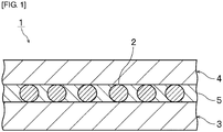
- Fig. 1 is a sectional view showing one example of a semiconductor sensor including an adhesive for semiconductor mounting according to the present invention.
- An adhesive for semiconductor mounting according to the present invention (hereinafter, sometimes indicated as an adhesive) is an adhesive used for mounting a semiconductor.
- the adhesive according to the present invention contains a silicone resin and a spacer.
- the content of the spacer contained in the adhesive according to the present invention is 0.1% by weight or more and 5% by weight or less in 100% by weight of the adhesive.
- the 10% compressive elasticity modulus of the spacer is 5000 N/mm 2 or more and 15000 N/mm 2 or less.
- the average particle diameter of the spacer is 10 ⁇ m or more and 200 ⁇ m or less.
- the adhesive can have the specifications described above to achieve high-precision gap control and increase heat resistance in the mounting of a semiconductor.
- the adhesive enables more horizontal adhesion of a semiconductor chip.
- the adhesive can increase, as the heat resistance, adhesion strength at a high temperature.
- the content of the spacer is 0.1% by weight or more and 5% by weight or less in 100% by weight of the adhesive.
- the content of the spacer is, in 100% by weight of the adhesive, preferably 0.5% by weight or more, more preferably 1% by weight or more and preferably 4% by weight or less, more preferably 3% by weight or less.
- the 10% compressive elasticity modulus is a compressive elasticity modulus when the spacer is compressed by 10%.
- the 10% compressive elasticity modulus of the spacer is 5000 N/mm 2 or more and 15000 N/mm 2 or less.
- the 10% compressive elasticity modulus of the spacer is preferably 5500 N/mm 2 or more, more preferably 6000 N/mm 2 or more and preferably 10000 N/mm 2 or less, more preferably 8000 N/mm 2 or less.
- the 10% compressive elasticity modulus of the spacer can be measured as follows.
- the spacer is compressed with a smooth flat end surface of a cylindrical indenter (diameter 50 ⁇ m, made of diamond) of a micro compression testing machine under the loading conditions of 25°C and a maximum test load of 20 mN for 60 seconds.
- a load value (N) and a compressive displacement (mm) are measured.
- the compressive elasticity modulus can be derived from the following equation.
- the average particle diameter of the spacer is 10 ⁇ m or more and 200 ⁇ m or less.
- the average particle diameter of the spacer is preferably 20 ⁇ m or more, more preferably 30 ⁇ m or more and preferably 150 ⁇ m or less, more preferably 110 ⁇ m or less, further preferably 100 ⁇ m or less.
- the average particle diameter is derived by observing the spacer with a scanning electron microscope and arithmetically averaging the maximum diameters of any 50 spacer particles selected in the image observed.
- the ratio of the 10% compressive elasticity modulus of the spacer after the heating to the 10% compressive elasticity modulus of the spacer before the heating is preferably 0.95 or more, more preferably 0.98 or more and preferably 1.05 or less, more preferably 1.02 or less.
- the spacer contained in the adhesive preferably includes no spacer particles having an average particle diameter of 1.5 times or more the average particle diameter of the spacer.
- the spacer contained in the adhesive includes spacer particles having an average particle diameter of 1.5 times or more the average particle diameter of the spacer, the spacer includes, in all 100% spacer particles, preferably 0.1% or less of spacer particles, more preferably 0.05% or less of spacer particles having an average particle diameter of 1.5 times or more the average particle diameter of the spacer, for further increasing the gap control effect.
- the specific gravity of the spacer is preferably 1.05 or more, more preferably 1.10 or more and preferably less than 1.30, more preferably less than 1.25.
- the difference is preferably 0.5 or less between the specific gravity of the adhesive that excludes the spacer and has been cured and the specific gravity of the spacer.
- the compression recovery rate of the spacer is preferably 50% or more, more preferably 60% or more. No upper limitation is particularly set for the compression recovery rate of the spacer.
- the compression recovery rate of the spacer may be 100% or less.
- the compression recovery rate of the spacer can be measured as follows.
- the spacer is sprayed on a sample stand.
- a load (reverse load value) is applied to one sprayed spacer particle toward the center of the spacer particle with a micro compression testing machine so that the spacer particle is deformed through compression by 30%. Subsequently, the load is released to an initial load value (0.40 mN). Loads-compressive displacements during this procedure are measured, and the compression recovery rate can be derived from the following equation.
- the loading rate is set to 0.33 mN/sec.
- the spacer is preferably a polymer of a polymerization component.
- the polymerization component is a component that can be polymerized.
- the polymerization component preferably includes a polymerizable monomer having an ethylenic unsaturated group.
- Examples of the polymerizable monomer having an ethylenic unsaturated group include a non-crosslinkable monomer and a crosslinkable monomer.
- non-crosslinkable monomer examples include, as vinyl compounds, styrene monomers such as styrene, ⁇ -methylstyrene, and chlorostyrene; vinyl ether compounds such as methyl vinyl ether, ethyl vinyl ether, propyl vinyl ether, 1,4-butanediol divinyl ether, cyclohexane dimethanol divinyl ether, and diethylene glycol divinyl ether; acid vinyl ester compounds such as vinyl acetate, vinyl butyrate, vinyl laurate, and vinyl stearate; and halogen-containing monomers such as vinyl chloride and vinyl fluoride, include, as (meth)acrylic compounds, alkyl (meth)acrylate compounds such as methyl (meth)acrylate, ethyl (meth)acrylate, propyl (meth)acrylate, butyl (meth)acrylate, 2-ethylhexyl (meth)acrylate, lauryl (meth)
- crosslinkable monomer examples include, as vinyl compounds, vinyl monomers such as divinylbenzene, 1,4-divinyloxybutane, and divinylsulfone, include, as (meth)acrylic compounds, polyfunctional (meth)acrylate compounds such as tetramethylolmethane tetra(meth)acrylate, tetramethylolmethane tri(meth)acrylate, tetramethylolmethane di(meth)acrylate, trimethylolpropane tri(meth)acrylate, dipentaerythritol hexa(meth)acrylate, dipentaerythritol penta(meth)acrylate, glycerol tri(meth)acrylate, glycerol di(meth)acrylate, (poly)ethylene glycol di(meth)acrylate, (poly)propylene glycol di(meth)acrylate, (poly)tetramethylene glycol di(meth)acrylate
- (meth)acrylate denotes an acrylate and a methacrylate.
- (meth)acrylic denotes acrylic and methacrylic.
- (meth)acryloyl denotes acryloyl and methacryloyl.
- the polymerization component preferably includes a vinyl compound or a (meth)acrylic compound.
- the spacer is preferably a copolymer of a polymerization component including divinylbenzene.
- the spacer is preferably a copolymer of a polymerization component including a (meth)acrylic compound, the (meth)acrylic compound including a (meth)acrylic compound having four or more (meth)acryloyl groups.
- Examples of the (meth)acrylic compound having four or more (meth)acryloyl groups include dipentaerythritol penta(meth)acrylate, dipentaerythritol hexa(meth)acrylate, ditrimethylolpropane tetra(meth)acrylate, pentaerythritol tetra(meth)acrylate, and tetramethylolmethane tetra(meth)acrylate.
- the polymerizable group residual rate of the spacer is preferably less than 1%, more preferably less than 0.5%.
- the polymerizable group residual rate of the spacer can be measured as follows.
- the spacer in an amount of 0.4 g is charged into a 8 mm rotor for solids of a nuclear magnetic resonance apparatus, and then measurement of 13 C is performed according to a Single Pulse (DD/MAS) method (measurement conditions: MAS rotation rate 7 kHz, number of scans 1000 times).
- the polymerizable group residual rate is calculated from a peak attributed to a vinyl group in the DD/MAS spectrum obtained.
- the nuclear magnetic resonance apparatus there can be used, for example, "JNM-ECX400" manufactured by JEOL RESONANCE Inc.
- the adhesive contains the spacer and the silicone resin that are described above.
- the spacer is preferably dispersed in the silicone resin and constitutes the adhesive.
- a semiconductor sensor requires, of an adhesive, high gapping performance and high heat resistance, so that the adhesive described above is suitably used for mounting a semiconductor sensor chip.
- a semiconductor sensor requires, of an adhesive, high gapping performance and high heat resistance, so that the adhesive described above is preferably an adhesive for mounting of a semiconductor sensor chip.
- the silicone resin preferably has fluidity.
- the silicone resin is preferably a paste.
- the paste includes a liquid.
- the adhesive may be a one-pack type including, for example, a main agent and a curing agent that have been mixed in advance, or a two-pack type including a main agent and a curing agent that are separate from each other.
- the adhesive may be a condensation curing type or an addition curing type.
- the adhesive may be cured with use of a catalyst such as platinum or may be cured by heating or moisture.
- the silicone resin is not particularly limited.
- the silicone resin may be an organopolysiloxane compound, and the organopolysiloxane may have a hydroxyl group or a vinyl group at a terminal.
- the silicone resin may be polypropyleneoxide having a methyldimethoxysilyl group.
- the adhesive may contain, in addition to the silicone resin and the spacer, a vinyl resin, a thermoplastic resin, a curable resin, a thermoplastic block copolymer, an elastomer, and a solvent, for example. These components may be used singly or in combination of two or more components.
- Examples of the vinyl resin include a vinyl acetate resin, an acrylic resin, and a styrene resin.
- examples of the thermoplastic resin include a polyolefin resin, an ethylene-vinyl acetate copolymer, and a polyamide resin.
- examples of the curable resin include an epoxy resin, a urethane resin, a polyimide resin, and an unsaturated polyester resin.
- the curable resin may be a normal temperature curing resin, a thermosetting resin, a photocuring resin, or a moisture curing resin. These curable resins may be used in combination with a curing agent.
- thermoplastic block copolymer examples include a styrene-butadiene-styrene block copolymer, a styrene-isoprene-styrene block copolymer, a hydrogenated product of a styrene-butadiene-styrene block copolymer, and a hydrogenated product of a styrene-isoprene-styrene block copolymer.
- the elastomer examples include a styrene-butadiene copolymer rubber and an acrylonitrile-styrene block copolymer rubber.
- the solvent examples include water and an organic solvent.
- An organic solvent is preferable for easy removal.
- the organic solvent include alcohol compounds such as ethanol, ketone compounds such as acetone, methyl ethyl ketone, and cyclohexanone, aromatic hydrocarbon compounds such as toluene, xylene, and tetramethylbenzene, glycol ether compounds such as cellosolve, methyl cellosolve, butyl cellosolve, carbitol, methyl carbitol, butyl carbitol, propylene glycol monomethyl ether, dipropylene glycol monomethyl ether, dipropylene glycol diethyl ether, and tripropylene glycol monomethyl ether, ester compounds such as ethyl acetate, butyl acetate, butyl lactate, cellosolve acetate, butyl cellosolve acetate, carbitol acetate, butyl carbitol acetate, propylene glyco
- the adhesive may contain, in addition to the spacer and the silicone resin, a variety of additives such as a filler, an extender, a softener, a plasticizer, a polymerization catalyst, a curing catalyst, a coloring agent, an antioxidant, a thermal stabilizer, a light stabilizer, a UV absorber, a lubricant, an antistatic agent, and a flame retardant, for example.
- additives such as a filler, an extender, a softener, a plasticizer, a polymerization catalyst, a curing catalyst, a coloring agent, an antioxidant, a thermal stabilizer, a light stabilizer, a UV absorber, a lubricant, an antistatic agent, and a flame retardant, for example.
- a conventionally known dispersing method can be used, and the method is not particularly limited.
- the method of dispersing the spacer in the silicone resin include a method of adding the spacer into the silicone resin and then kneading the mixture with, for example, a planetary mixer for dispersion, a method of uniformly dispersing the spacer in water or an organic solvent with, for example, a homogenizer, then adding the water or organic solvent containing the spacer into the silicone resin, and kneading the mixture with, for example, a planetary mixer for dispersion, and a method of diluting the silicone resin with, for example, water or an organic solvent, then adding the spacer to the diluted silicone resin, and kneading the mixture with, for example, a planetary mixer for dispersion.
- the content of the silicone resin is, in 100% by weight of the adhesive, preferably 70% by weight or more, more preferably 80% by weight or more and preferably 99% by weight or less, more preferably 95% by weight or less.
- a semiconductor sensor according to the present invention includes a first member, a semiconductor as a second member, and an adhesive layer that bonds the first member to the second member.
- the adhesive layer is formed of a cured product of the adhesive described above.
- the second member as a semiconductor is preferably a semiconductor sensor chip.
- Fig. 1 is a sectional view showing one example of a semiconductor sensor including the adhesive for semiconductor mounting according to the present invention.
- a semiconductor sensor 1 shown in Fig. 1 includes a first member 3, a semiconductor sensor chip as a second member 4, and an adhesive layer 5 that bonds the first member 3 to the second member 4.
- the adhesive layer 5 is a cured product of an adhesive containing a spacer 2 and a silicone resin.
- the spacer 2 is present between the first member 3 and the second member 4, so that the first member 3 is horizontally bonded to the second member 4 with a fixed interval (gap) between the members.
- a method of manufacturing the semiconductor sensor is not particularly limited.
- the method of manufacturing the semiconductor sensor there can be exemplified a method of disposing the adhesive between the first member and the second member to give a stacked body and then heating and pressurizing the stacked body.
- the first member include electronic components such as a semiconductor chip, a capacitor, and a diode, and electronic components such as a circuit substrate, e.g., a printed substrate, a flexible printed substrate, a glass epoxy substrate, and a glass substrate.
- the first member is preferably an electronic component.
- the adhesive is preferably an adhesive for bonding an electronic component.
- the semiconductor is preferably a sensor chip, more preferably a pressure sensor chip.
- the first member may include a first electrode on a surface thereof.
- the second member may include a second electrode on a surface thereof.
- the electrodes provided on the members include metal electrodes such as a gold electrode, a nickel electrode, a tin electrode, an aluminum electrode, a copper electrode, a silver electrode, a titanium electrode, a molybdenum electrode, and a tungsten electrode.
- the electrode is preferably a gold electrode, a nickel electrode, a titanium electrode, a tin electrode, or a copper electrode.
- the electrode is preferably an aluminum electrode, a titanium electrode, a copper electrode, a molybdenum electrode, or a tungsten electrode.
- the electrode When the electrode is an aluminum electrode, the electrode may be an electrode formed of only aluminum or an electrode obtained by stacking an aluminum layer on a surface of a metal oxide layer.
- a material for the metal oxide layer there can be exemplified indium oxide doped with a trivalent metal element and zinc oxide doped with a trivalent metal element. Examples of the trivalent metal element include Sn, Al, and Ga.
- a monomer mixed liquid was obtained by mixing and uniformly dissolving 500 g of tetramethylolmethane, 500 g of divinylbenzene, and 20 g of benzoyl peroxide.
- a 1% by weight aqueous solution of polyvinyl alcohol in an amount of 5 kg was prepared and charged into a reaction vessel.
- the monomer mixed liquid was further charged into this reaction vessel and stirred for 2 to 4 hours, to adjust the particle diameter of a liquid drop of the monomer mixed liquid so that a predetermined particle diameter was given.
- a reaction was performed in a nitrogen atmosphere at 85°C for 10 hours to give a spacer 1.
- the spacer 1 obtained was washed with hot water several times and then subjected to classification operations. In the spacer 1 obtained, the average particle diameter was 19.8 ⁇ m and the CV value of the particle diameter was 3.5%.
- a monomer mixed liquid was obtained by mixing and uniformly dissolving 1000 g of divinylbenzene and 56 g of benzoyl peroxide.
- a 1% by weight aqueous solution of polyvinyl alcohol in an amount of 5 kg was prepared and charged into a reaction vessel.
- the monomer mixed liquid was further charged into this reaction vessel and stirred for 2 to 4 hours, to adjust the particle diameter of a liquid drop of the monomer mixed liquid so that a predetermined particle diameter was given.
- a reaction was performed in a nitrogen atmosphere at 90°C for 10 hours to give a spacer 2.
- the spacer 2 obtained was washed with hot water several times and then subjected to classification operations. In the spacer 2 obtained, the average particle diameter was 20.1 ⁇ m and the CV value of the particle diameter was 3.2%.
- a monomer mixed liquid was obtained by mixing and uniformly dissolving 800 g of divinylbenzene, 200 g of acrylonitrile, and 20 g of benzoyl peroxide.
- a 1% by weight aqueous solution of polyvinyl alcohol in an amount of 5 kg was prepared and charged into a reaction vessel.
- the monomer mixed liquid was further charged into this reaction vessel and stirred for 2 to 4 hours, to adjust the particle diameter of a liquid drop of the monomer mixed liquid so that a predetermined particle diameter was given.
- a reaction was performed in a nitrogen atmosphere at 140°C for 6 hours to give a spacer 3.
- the spacer 3 obtained was washed with hot water several times and then subjected to classification operations. In the spacer 3 obtained, the average particle diameter was 20.5 ⁇ m and the CV value of the particle diameter was 2.9%.
- a monomer mixed liquid was obtained by mixing 400 g of methyltrimethoxysilane and 1600 g of vinyltrimethoxysilane.
- the monomer mixed liquid in an amount of 1000 g was added into a mixed liquid containing 100 g of methanol and 30 kg of ion-exchanged water (adjusted with ammonia water to give a pH of 10.5) at 15°C and reacted under stirring.
- the monomer mixed liquid in an amount of 1000 g was added 48 hours after the first addition of the monomer mixed liquid.
- the reaction was performed for another 48 hours after the second addition of the monomer mixed liquid.
- the resultant product was washed with water and methanol several times and then dried under vacuum at 50°C for 48 hours to give dried particles.
- the dried particles were fired in a nitrogen atmosphere at 375°C for 10 hours to give a spacer.
- the spacer obtained was subjected to classification operations to give a spacer 4. In the spacer 4 obtained, the average particle diameter was 19.0 ⁇ m and the CV value of the particle diameter was 4.7 ⁇ m.
- a monomer mixed liquid was obtained by mixing and uniformly dissolving 100 g of ethylene glycol dimethacrylate, 800 g of isobornyl acrylate, 100g of cyclohexyl methacrylate, and 35 g of benzoyl peroxide.
- a 1% by weight aqueous solution of polyvinyl alcohol in an amount of 5 kg was prepared and charged into a reaction vessel.
- the monomer mixed liquid was further charged into this reaction vessel and stirred for 2 to 4 hours, to adjust the particle diameter of a liquid drop of the monomer mixed liquid so that a predetermined particle diameter was given.
- a reaction was performed in a nitrogen atmosphere at 90°C for 9 hours to give a spacer A.
- the spacer A obtained was washed with hot water several times and then subjected to classification operations. In the spacer A obtained, the average particle diameter was 20.1 ⁇ m and the CV value of the particle diameter was 3.1%.
- a solution A was prepared by dissolving 0.5 parts by weight of tert-butyl-2-ethylperoxyhexanoate (polymerization initiator, "PERBUTYL O” manufactured by NOF CORPORATION) in 30 parts by weight of a both terminal acrylic silicone oil.
- polymerization initiator "PERBUTYL O” manufactured by NOF CORPORATION
- an aqueous solution B was prepared by mixing 150 parts by weight of ion-exchanged water, 0.8 parts by weight of a 40% by weight aqueous solution of triethanolamine lauryl sulfate (emulsifier), and 80 parts by weight of a 5% by weight aqueous solution of polyvinyl alcohol (degree of polymerization: about 2000, degree of saponification: 86.5 to 89 mol%, "GOHSENOL GH-20" manufactured by The Nippon Synthetic Chemical Industry Co., Ltd.).
- the solution A was charged and then the aqueous solution B was added.
- SPG Shirasu Porous Glass
- the spacer 1 was added to a one-component thermally curable silicone adhesive TSE322 (manufactured by Momentive Performance Materials Inc.) so that the content of the spacer 1 became 1% by weight in an adhesive to be obtained, and was stirred with a planetary mixer for uniform dispersion.
- a silicone adhesive was prepared.
- the silicone adhesive was charged into a syringe and applied to a printed substrate with use of a dispenser so that the thickness of the adhesive became 20 ⁇ m, and a pressure sensor chip was disposed on the applied adhesive and heated at 150°C for 10 minutes for adhesive bonding to give a pressure sensor structure.
- a pressure sensor structure was obtained in the same manner as in Example 1 except that the spacer 2 was used in place of the spacer 1 in the preparation of the silicone adhesive.
- a pressure sensor structure was obtained in the same manner as in Example 1 except that in the preparation of the silicone adhesive, the spacer 3 was used in place of the spacer 1 and the spacer 3 was added to the silicone adhesive so that the content of the spacer 3 became 0.5% by weight in the adhesive to be obtained.
- a pressure sensor structure was obtained in the same manner as in Example 1 except that the spacer 3 was used in place of the spacer 1 in the preparation of the silicone adhesive.
- a pressure sensor structure was obtained in the same manner as in Example 1 except that in the preparation of the silicone adhesive, the spacer 3 was used in place of the spacer 1 and the spacer 3 was added to the silicone adhesive so that the content of the spacer 3 became 3% by weight in the adhesive to be obtained.
- a pressure sensor structure was obtained in the same manner as in Example 1 except that in the preparation of the silicone adhesive, the spacer 4 was used in place of the spacer 1 and the spacer 4 was added to the silicone adhesive so that the content of the spacer 4 became 2.5% by weight in the adhesive to be obtained.
- a pressure sensor structure was obtained in the same manner as in Example 1 except that in the preparation of the silicone adhesive, the spacer A was used in place of the spacer 1 and the spacer A was added to the silicone adhesive so that the content of the spacer A became 8% by weight in the adhesive to be obtained.
- a pressure sensor structure was obtained in the same manner as in Example 1 except that in the preparation of the silicone adhesive, the spacer B was used in place of the spacer 1 and the spacer B was added to the silicone adhesive so that the content of the spacer B became 10% by weight in the adhesive to be obtained.
- the spacers were measured for the 10% compressive elasticity modulus by the method described above with use of "Fischerscope H100" manufactured by HELMUT FISCHER GMBH.
- the average particle diameter of each of the spacers was derived by observing the spacer with a scanning electron microscope (SEM) and arithmetically averaging the maximum particle diameters of any 50 spacer particles selected in the image observed.
- SEM scanning electron microscope
- the spacers were measured for the compression recovery rate by the method described above with use of "Fischerscope H100" manufactured by HELMUT FISCHER GMBH.
- the spacers were measured for the 10% compressive elasticity modulus after subjected to heating in the atmosphere at 150°C for 1000 hours with use of "Fischerscope H100" manufactured by HELMUT FISCHER GMBH.
- the change of the spacers with heating and time was determined according to the following criteria.
- Each of the pressure sensor structures obtained was observed with a scanning electron microscope (SEM) and evaluated for the minimum thickness and the maximum thickness of the adhesive layer.
- the gap control property was determined according to the following criteria.
- connection strength was determined from the shear strength.
- connection strength [Criteria for determining heat resistance: connection strength]
Landscapes
- Chemical & Material Sciences (AREA)
- Organic Chemistry (AREA)
- Chemical Kinetics & Catalysis (AREA)
- Physics & Mathematics (AREA)
- General Physics & Mathematics (AREA)
- Medicinal Chemistry (AREA)
- Health & Medical Sciences (AREA)
- Polymers & Plastics (AREA)
- Adhesives Or Adhesive Processes (AREA)
- Measuring Fluid Pressure (AREA)
- Engineering & Computer Science (AREA)
- Microelectronics & Electronic Packaging (AREA)
- Die Bonding (AREA)
- Compositions Of Macromolecular Compounds (AREA)
Applications Claiming Priority (3)
| Application Number | Priority Date | Filing Date | Title |
|---|---|---|---|
| JP2016047173 | 2016-03-10 | ||
| JP2016047174 | 2016-03-10 | ||
| PCT/JP2017/009815 WO2017155116A1 (ja) | 2016-03-10 | 2017-03-10 | 半導体実装用接着剤及び半導体センサ |
Publications (3)
| Publication Number | Publication Date |
|---|---|
| EP3428599A1 true EP3428599A1 (de) | 2019-01-16 |
| EP3428599A4 EP3428599A4 (de) | 2019-09-25 |
| EP3428599B1 EP3428599B1 (de) | 2023-06-07 |
Family
ID=59790414
Family Applications (2)
| Application Number | Title | Priority Date | Filing Date |
|---|---|---|---|
| EP17763449.0A Active EP3428600B1 (de) | 2016-03-10 | 2017-03-10 | Klebstoff für halbleitersensorchipmontage und halbleitersensor |
| EP17763448.2A Active EP3428599B1 (de) | 2016-03-10 | 2017-03-10 | Klebstoff für halbleitermontage und halbleitersensor |
Family Applications Before (1)
| Application Number | Title | Priority Date | Filing Date |
|---|---|---|---|
| EP17763449.0A Active EP3428600B1 (de) | 2016-03-10 | 2017-03-10 | Klebstoff für halbleitersensorchipmontage und halbleitersensor |
Country Status (7)
| Country | Link |
|---|---|
| US (2) | US10679925B2 (de) |
| EP (2) | EP3428600B1 (de) |
| JP (4) | JP6322336B2 (de) |
| KR (3) | KR20220019061A (de) |
| CN (2) | CN108139286B (de) |
| TW (2) | TWI751142B (de) |
| WO (2) | WO2017155116A1 (de) |
Families Citing this family (6)
| Publication number | Priority date | Publication date | Assignee | Title |
|---|---|---|---|---|
| WO2017082353A1 (ja) * | 2015-11-11 | 2017-05-18 | 積水化学工業株式会社 | 粒子、粒子材料、接続材料及び接続構造体 |
| US10679925B2 (en) * | 2016-03-10 | 2020-06-09 | Sekisui Chemical Co., Ltd. | Adhesive for semiconductor mounting, and semiconductor sensor |
| WO2019230881A1 (ja) * | 2018-05-31 | 2019-12-05 | 積水化学工業株式会社 | スペーサ粒子、接着剤及び接着構造体 |
| EP3796373B1 (de) | 2019-09-20 | 2023-06-28 | BIOTRONIK SE & Co. KG | Platinenanordnung eines implantierbaren medizinischen geräts |
| US20230140786A1 (en) * | 2019-10-15 | 2023-05-04 | Sekisui Chemical Co., Ltd. | Gap material, adhesive, and display device |
| KR102584513B1 (ko) * | 2020-12-31 | 2023-10-06 | 세메스 주식회사 | 온도 변화가 수반되는 분위기에 제공되는 기판 지지 부재의 수평 측정용 기판형 센서, 이를 이용한 수평 측정 방법 및 비일시적 컴퓨터 판독가능 매체 |
Family Cites Families (30)
| Publication number | Priority date | Publication date | Assignee | Title |
|---|---|---|---|---|
| JP3445641B2 (ja) | 1993-07-30 | 2003-09-08 | 株式会社デンソー | 半導体装置 |
| JPH10300772A (ja) | 1997-04-24 | 1998-11-13 | Denso Corp | 半導体加速度センサ |
| JP3384949B2 (ja) | 1997-06-26 | 2003-03-10 | 日新製鋼株式会社 | 耐汚染性に優れた金属パネル |
| JPH11108782A (ja) * | 1997-10-02 | 1999-04-23 | Denso Corp | 半導体力学量センサ |
| CN1900195B (zh) | 1998-08-13 | 2011-06-22 | 日立化成工业株式会社 | 电路构件连接用的粘结剂、电路板及其制造方法 |
| JP2003322573A (ja) * | 2002-04-30 | 2003-11-14 | Fujikura Ltd | 電子デバイスの取付構造 |
| JP2005294044A (ja) * | 2004-03-31 | 2005-10-20 | Sekisui Chem Co Ltd | 導電性微粒子、及び接続構造体 |
| JP4839041B2 (ja) | 2005-08-29 | 2011-12-14 | 東レ・ダウコーニング株式会社 | 絶縁性液状ダイボンディング剤および半導体装置 |
| JP4802667B2 (ja) | 2005-11-08 | 2011-10-26 | 住友金属鉱山株式会社 | エポキシ樹脂接着組成物及びそれを用いた光半導体用接着剤 |
| EP2322585A1 (de) | 2005-12-26 | 2011-05-18 | Hitachi Chemical Co., Ltd. | Haftmasse, schaltkreisverbindendes Material sowie Verbindungsstruktur eines Schaltkreiselements |
| JP4269292B2 (ja) | 2006-05-30 | 2009-05-27 | 日立金属株式会社 | 3軸加速度センサー |
| EP2045839A4 (de) * | 2006-07-20 | 2009-08-05 | Sekisui Chemical Co Ltd | Kleber für elektronische komponenten, verfahren zum herstellen eines halbleiterchip-laminats und halbleiteranordnung |
| CN103205231A (zh) | 2006-07-21 | 2013-07-17 | 日立化成工业株式会社 | 电路连接材料、电路部件的连接结构及电路部件的连接方法 |
| JP5108556B2 (ja) * | 2007-02-27 | 2012-12-26 | 積水化成品工業株式会社 | アクリル系樹脂粒子の製造方法及び樹脂粒子の製造方法 |
| US20090050266A1 (en) * | 2007-08-21 | 2009-02-26 | Kang Yang | Crosslinked polymeric materials as filler and spacers in adhesives |
| WO2009044706A1 (ja) | 2007-10-02 | 2009-04-09 | Hitachi Chemical Company, Ltd. | 回路接続材料、回路端子の接続構造 |
| JP5118956B2 (ja) | 2007-12-26 | 2013-01-16 | 積水化学工業株式会社 | 電子部品用接着剤 |
| CN102112507B (zh) * | 2008-07-31 | 2013-12-11 | 积水化学工业株式会社 | 聚合物粒子、导电性粒子、各向异性导电材料以及连接结构体 |
| JP5287763B2 (ja) | 2010-02-24 | 2013-09-11 | 株式会社デンソー | センサ装置およびその製造方法 |
| JP2011198953A (ja) * | 2010-03-18 | 2011-10-06 | Sekisui Chem Co Ltd | 電子部品積層体の製造方法 |
| JP2010237686A (ja) * | 2010-05-21 | 2010-10-21 | Sekisui Chem Co Ltd | 液晶表示装置の製造方法 |
| JP2012004224A (ja) | 2010-06-15 | 2012-01-05 | Sekisui Chem Co Ltd | 電子部品接合体の製造方法及び電子部品接合体 |
| JP2012060020A (ja) * | 2010-09-10 | 2012-03-22 | Sekisui Chem Co Ltd | 半導体チップ実装体の製造方法及び半導体装置 |
| KR101374365B1 (ko) | 2010-12-27 | 2014-03-17 | 제일모직주식회사 | 반도체용 접착 조성물 및 이를 포함하는 접착 필름 |
| JP5583714B2 (ja) * | 2011-04-01 | 2014-09-03 | 株式会社日本触媒 | 導電性微粒子及びそれを用いた異方性導電材料 |
| MY165741A (en) * | 2011-09-27 | 2018-04-23 | Sekisui Plastics | Spacer particle for resin composition layer and use thereof |
| US20140120356A1 (en) | 2012-06-18 | 2014-05-01 | Ormet Circuits, Inc. | Conductive film adhesive |
| JP6131819B2 (ja) | 2013-10-10 | 2017-05-24 | 株式会社デンソー | 圧力センサ |
| US9607086B2 (en) * | 2014-03-27 | 2017-03-28 | Mcafee, Inc. | Providing prevalence information using query data |
| US10679925B2 (en) * | 2016-03-10 | 2020-06-09 | Sekisui Chemical Co., Ltd. | Adhesive for semiconductor mounting, and semiconductor sensor |
-
2017
- 2017-03-10 US US16/082,430 patent/US10679925B2/en active Active
- 2017-03-10 JP JP2017516172A patent/JP6322336B2/ja active Active
- 2017-03-10 EP EP17763449.0A patent/EP3428600B1/de active Active
- 2017-03-10 US US16/082,491 patent/US10790217B2/en active Active
- 2017-03-10 CN CN201780003507.4A patent/CN108139286B/zh active Active
- 2017-03-10 WO PCT/JP2017/009815 patent/WO2017155116A1/ja not_active Ceased
- 2017-03-10 TW TW106108073A patent/TWI751142B/zh active
- 2017-03-10 KR KR1020227002671A patent/KR20220019061A/ko not_active Ceased
- 2017-03-10 KR KR1020187006708A patent/KR102356926B1/ko active Active
- 2017-03-10 CN CN201780003503.6A patent/CN108139285B/zh active Active
- 2017-03-10 EP EP17763448.2A patent/EP3428599B1/de active Active
- 2017-03-10 TW TW106108074A patent/TWI725131B/zh active
- 2017-03-10 WO PCT/JP2017/009816 patent/WO2017155117A1/ja not_active Ceased
- 2017-03-10 JP JP2017516173A patent/JP6322337B2/ja active Active
- 2017-03-10 KR KR1020187006709A patent/KR102331523B1/ko active Active
-
2018
- 2018-04-05 JP JP2018073140A patent/JP2018135525A/ja active Pending
- 2018-04-05 JP JP2018073139A patent/JP6971192B2/ja active Active
Also Published As
| Publication number | Publication date |
|---|---|
| JPWO2017155117A1 (ja) | 2018-03-15 |
| EP3428599B1 (de) | 2023-06-07 |
| CN108139285B (zh) | 2021-06-04 |
| TWI725131B (zh) | 2021-04-21 |
| KR20180118102A (ko) | 2018-10-30 |
| CN108139285A (zh) | 2018-06-08 |
| EP3428600A1 (de) | 2019-01-16 |
| TW201800546A (zh) | 2018-01-01 |
| EP3428600A4 (de) | 2019-09-25 |
| EP3428599A4 (de) | 2019-09-25 |
| KR102331523B1 (ko) | 2021-11-26 |
| CN108139286A (zh) | 2018-06-08 |
| WO2017155117A1 (ja) | 2017-09-14 |
| WO2017155116A1 (ja) | 2017-09-14 |
| JPWO2017155116A1 (ja) | 2018-03-15 |
| KR20220019061A (ko) | 2022-02-15 |
| JP6971192B2 (ja) | 2021-11-24 |
| CN108139286B (zh) | 2021-06-25 |
| US20190088573A1 (en) | 2019-03-21 |
| US10790217B2 (en) | 2020-09-29 |
| JP2018135525A (ja) | 2018-08-30 |
| JP6322337B2 (ja) | 2018-05-09 |
| US20190078002A1 (en) | 2019-03-14 |
| EP3428600B1 (de) | 2023-05-24 |
| KR20180117589A (ko) | 2018-10-29 |
| TW201800545A (zh) | 2018-01-01 |
| JP2018142709A (ja) | 2018-09-13 |
| TWI751142B (zh) | 2022-01-01 |
| US10679925B2 (en) | 2020-06-09 |
| KR102356926B1 (ko) | 2022-01-28 |
| JP6322336B2 (ja) | 2018-05-09 |
Similar Documents
| Publication | Publication Date | Title |
|---|---|---|
| EP3428599B1 (de) | Klebstoff für halbleitermontage und halbleitersensor | |
| WO2019050011A1 (ja) | 回路接続用接着剤フィルム及びその製造方法、回路接続構造体の製造方法、並びに、接着剤フィルム収容セット | |
| CN109196072B (zh) | 接合用组合物、光学用粘接剂以及压力传感器用粘接剂 | |
| WO2017090693A1 (ja) | 接着剤組成物及び構造体 | |
| JP7316223B2 (ja) | スペーサ粒子、接着剤及び接着構造体 | |
| CN120418930A (zh) | 树脂膜形成用片 |
Legal Events
| Date | Code | Title | Description |
|---|---|---|---|
| STAA | Information on the status of an ep patent application or granted ep patent |
Free format text: STATUS: THE INTERNATIONAL PUBLICATION HAS BEEN MADE |
|
| PUAI | Public reference made under article 153(3) epc to a published international application that has entered the european phase |
Free format text: ORIGINAL CODE: 0009012 |
|
| STAA | Information on the status of an ep patent application or granted ep patent |
Free format text: STATUS: REQUEST FOR EXAMINATION WAS MADE |
|
| 17P | Request for examination filed |
Effective date: 20180910 |
|
| AK | Designated contracting states |
Kind code of ref document: A1 Designated state(s): AL AT BE BG CH CY CZ DE DK EE ES FI FR GB GR HR HU IE IS IT LI LT LU LV MC MK MT NL NO PL PT RO RS SE SI SK SM TR |
|
| AX | Request for extension of the european patent |
Extension state: BA ME |
|
| DAV | Request for validation of the european patent (deleted) | ||
| DAX | Request for extension of the european patent (deleted) | ||
| A4 | Supplementary search report drawn up and despatched |
Effective date: 20190827 |
|
| RIC1 | Information provided on ipc code assigned before grant |
Ipc: G01L 9/00 20060101AFI20190821BHEP Ipc: C09J 11/00 20060101ALI20190821BHEP Ipc: C09J 11/08 20060101ALI20190821BHEP Ipc: C09J 183/04 20060101ALI20190821BHEP Ipc: C09J 171/02 20060101ALI20190821BHEP Ipc: H01L 29/84 20060101ALI20190821BHEP |
|
| GRAP | Despatch of communication of intention to grant a patent |
Free format text: ORIGINAL CODE: EPIDOSNIGR1 |
|
| STAA | Information on the status of an ep patent application or granted ep patent |
Free format text: STATUS: GRANT OF PATENT IS INTENDED |
|
| INTG | Intention to grant announced |
Effective date: 20230104 |
|
| RIN1 | Information on inventor provided before grant (corrected) |
Inventor name: YAMADA, YASUYUKI Inventor name: UEDA, SAORI |
|
| GRAS | Grant fee paid |
Free format text: ORIGINAL CODE: EPIDOSNIGR3 |
|
| GRAA | (expected) grant |
Free format text: ORIGINAL CODE: 0009210 |
|
| STAA | Information on the status of an ep patent application or granted ep patent |
Free format text: STATUS: THE PATENT HAS BEEN GRANTED |
|
| AK | Designated contracting states |
Kind code of ref document: B1 Designated state(s): AL AT BE BG CH CY CZ DE DK EE ES FI FR GB GR HR HU IE IS IT LI LT LU LV MC MK MT NL NO PL PT RO RS SE SI SK SM TR |
|
| REG | Reference to a national code |
Ref country code: GB Ref legal event code: FG4D |
|
| REG | Reference to a national code |
Ref country code: CH Ref legal event code: EP Ref country code: AT Ref legal event code: REF Ref document number: 1576453 Country of ref document: AT Kind code of ref document: T Effective date: 20230615 |
|
| REG | Reference to a national code |
Ref country code: DE Ref legal event code: R096 Ref document number: 602017069632 Country of ref document: DE |
|
| P01 | Opt-out of the competence of the unified patent court (upc) registered |
Effective date: 20230523 |
|
| REG | Reference to a national code |
Ref country code: LT Ref legal event code: MG9D |
|
| REG | Reference to a national code |
Ref country code: NL Ref legal event code: MP Effective date: 20230607 |
|
| PG25 | Lapsed in a contracting state [announced via postgrant information from national office to epo] |
Ref country code: SE Free format text: LAPSE BECAUSE OF FAILURE TO SUBMIT A TRANSLATION OF THE DESCRIPTION OR TO PAY THE FEE WITHIN THE PRESCRIBED TIME-LIMIT Effective date: 20230607 Ref country code: NO Free format text: LAPSE BECAUSE OF FAILURE TO SUBMIT A TRANSLATION OF THE DESCRIPTION OR TO PAY THE FEE WITHIN THE PRESCRIBED TIME-LIMIT Effective date: 20230907 Ref country code: ES Free format text: LAPSE BECAUSE OF FAILURE TO SUBMIT A TRANSLATION OF THE DESCRIPTION OR TO PAY THE FEE WITHIN THE PRESCRIBED TIME-LIMIT Effective date: 20230607 |
|
| REG | Reference to a national code |
Ref country code: AT Ref legal event code: MK05 Ref document number: 1576453 Country of ref document: AT Kind code of ref document: T Effective date: 20230607 |
|
| PG25 | Lapsed in a contracting state [announced via postgrant information from national office to epo] |
Ref country code: RS Free format text: LAPSE BECAUSE OF FAILURE TO SUBMIT A TRANSLATION OF THE DESCRIPTION OR TO PAY THE FEE WITHIN THE PRESCRIBED TIME-LIMIT Effective date: 20230607 Ref country code: NL Free format text: LAPSE BECAUSE OF FAILURE TO SUBMIT A TRANSLATION OF THE DESCRIPTION OR TO PAY THE FEE WITHIN THE PRESCRIBED TIME-LIMIT Effective date: 20230607 Ref country code: LV Free format text: LAPSE BECAUSE OF FAILURE TO SUBMIT A TRANSLATION OF THE DESCRIPTION OR TO PAY THE FEE WITHIN THE PRESCRIBED TIME-LIMIT Effective date: 20230607 Ref country code: LT Free format text: LAPSE BECAUSE OF FAILURE TO SUBMIT A TRANSLATION OF THE DESCRIPTION OR TO PAY THE FEE WITHIN THE PRESCRIBED TIME-LIMIT Effective date: 20230607 Ref country code: HR Free format text: LAPSE BECAUSE OF FAILURE TO SUBMIT A TRANSLATION OF THE DESCRIPTION OR TO PAY THE FEE WITHIN THE PRESCRIBED TIME-LIMIT Effective date: 20230607 Ref country code: GR Free format text: LAPSE BECAUSE OF FAILURE TO SUBMIT A TRANSLATION OF THE DESCRIPTION OR TO PAY THE FEE WITHIN THE PRESCRIBED TIME-LIMIT Effective date: 20230908 |
|
| PG25 | Lapsed in a contracting state [announced via postgrant information from national office to epo] |
Ref country code: FI Free format text: LAPSE BECAUSE OF FAILURE TO SUBMIT A TRANSLATION OF THE DESCRIPTION OR TO PAY THE FEE WITHIN THE PRESCRIBED TIME-LIMIT Effective date: 20230607 |
|
| PG25 | Lapsed in a contracting state [announced via postgrant information from national office to epo] |
Ref country code: SK Free format text: LAPSE BECAUSE OF FAILURE TO SUBMIT A TRANSLATION OF THE DESCRIPTION OR TO PAY THE FEE WITHIN THE PRESCRIBED TIME-LIMIT Effective date: 20230607 |
|
| PG25 | Lapsed in a contracting state [announced via postgrant information from national office to epo] |
Ref country code: IS Free format text: LAPSE BECAUSE OF FAILURE TO SUBMIT A TRANSLATION OF THE DESCRIPTION OR TO PAY THE FEE WITHIN THE PRESCRIBED TIME-LIMIT Effective date: 20231007 |
|
| PG25 | Lapsed in a contracting state [announced via postgrant information from national office to epo] |
Ref country code: SM Free format text: LAPSE BECAUSE OF FAILURE TO SUBMIT A TRANSLATION OF THE DESCRIPTION OR TO PAY THE FEE WITHIN THE PRESCRIBED TIME-LIMIT Effective date: 20230607 Ref country code: SK Free format text: LAPSE BECAUSE OF FAILURE TO SUBMIT A TRANSLATION OF THE DESCRIPTION OR TO PAY THE FEE WITHIN THE PRESCRIBED TIME-LIMIT Effective date: 20230607 Ref country code: RO Free format text: LAPSE BECAUSE OF FAILURE TO SUBMIT A TRANSLATION OF THE DESCRIPTION OR TO PAY THE FEE WITHIN THE PRESCRIBED TIME-LIMIT Effective date: 20230607 Ref country code: PT Free format text: LAPSE BECAUSE OF FAILURE TO SUBMIT A TRANSLATION OF THE DESCRIPTION OR TO PAY THE FEE WITHIN THE PRESCRIBED TIME-LIMIT Effective date: 20231009 Ref country code: IS Free format text: LAPSE BECAUSE OF FAILURE TO SUBMIT A TRANSLATION OF THE DESCRIPTION OR TO PAY THE FEE WITHIN THE PRESCRIBED TIME-LIMIT Effective date: 20231007 Ref country code: EE Free format text: LAPSE BECAUSE OF FAILURE TO SUBMIT A TRANSLATION OF THE DESCRIPTION OR TO PAY THE FEE WITHIN THE PRESCRIBED TIME-LIMIT Effective date: 20230607 Ref country code: CZ Free format text: LAPSE BECAUSE OF FAILURE TO SUBMIT A TRANSLATION OF THE DESCRIPTION OR TO PAY THE FEE WITHIN THE PRESCRIBED TIME-LIMIT Effective date: 20230607 Ref country code: AT Free format text: LAPSE BECAUSE OF FAILURE TO SUBMIT A TRANSLATION OF THE DESCRIPTION OR TO PAY THE FEE WITHIN THE PRESCRIBED TIME-LIMIT Effective date: 20230607 |
|
| PG25 | Lapsed in a contracting state [announced via postgrant information from national office to epo] |
Ref country code: PL Free format text: LAPSE BECAUSE OF FAILURE TO SUBMIT A TRANSLATION OF THE DESCRIPTION OR TO PAY THE FEE WITHIN THE PRESCRIBED TIME-LIMIT Effective date: 20230607 |
|
| REG | Reference to a national code |
Ref country code: DE Ref legal event code: R097 Ref document number: 602017069632 Country of ref document: DE |
|
| PLBE | No opposition filed within time limit |
Free format text: ORIGINAL CODE: 0009261 |
|
| STAA | Information on the status of an ep patent application or granted ep patent |
Free format text: STATUS: NO OPPOSITION FILED WITHIN TIME LIMIT |
|
| PG25 | Lapsed in a contracting state [announced via postgrant information from national office to epo] |
Ref country code: DK Free format text: LAPSE BECAUSE OF FAILURE TO SUBMIT A TRANSLATION OF THE DESCRIPTION OR TO PAY THE FEE WITHIN THE PRESCRIBED TIME-LIMIT Effective date: 20230607 |
|
| PG25 | Lapsed in a contracting state [announced via postgrant information from national office to epo] |
Ref country code: SI Free format text: LAPSE BECAUSE OF FAILURE TO SUBMIT A TRANSLATION OF THE DESCRIPTION OR TO PAY THE FEE WITHIN THE PRESCRIBED TIME-LIMIT Effective date: 20230607 |
|
| 26N | No opposition filed |
Effective date: 20240308 |
|
| PG25 | Lapsed in a contracting state [announced via postgrant information from national office to epo] |
Ref country code: SI Free format text: LAPSE BECAUSE OF FAILURE TO SUBMIT A TRANSLATION OF THE DESCRIPTION OR TO PAY THE FEE WITHIN THE PRESCRIBED TIME-LIMIT Effective date: 20230607 Ref country code: IT Free format text: LAPSE BECAUSE OF FAILURE TO SUBMIT A TRANSLATION OF THE DESCRIPTION OR TO PAY THE FEE WITHIN THE PRESCRIBED TIME-LIMIT Effective date: 20230607 |
|
| REG | Reference to a national code |
Ref country code: CH Ref legal event code: PL |
|
| PG25 | Lapsed in a contracting state [announced via postgrant information from national office to epo] |
Ref country code: BG Free format text: LAPSE BECAUSE OF FAILURE TO SUBMIT A TRANSLATION OF THE DESCRIPTION OR TO PAY THE FEE WITHIN THE PRESCRIBED TIME-LIMIT Effective date: 20230607 |
|
| PG25 | Lapsed in a contracting state [announced via postgrant information from national office to epo] |
Ref country code: LU Free format text: LAPSE BECAUSE OF NON-PAYMENT OF DUE FEES Effective date: 20240310 |
|
| PG25 | Lapsed in a contracting state [announced via postgrant information from national office to epo] |
Ref country code: MC Free format text: LAPSE BECAUSE OF FAILURE TO SUBMIT A TRANSLATION OF THE DESCRIPTION OR TO PAY THE FEE WITHIN THE PRESCRIBED TIME-LIMIT Effective date: 20230607 |
|
| GBPC | Gb: european patent ceased through non-payment of renewal fee |
Effective date: 20240310 |
|
| PG25 | Lapsed in a contracting state [announced via postgrant information from national office to epo] |
Ref country code: MC Free format text: LAPSE BECAUSE OF FAILURE TO SUBMIT A TRANSLATION OF THE DESCRIPTION OR TO PAY THE FEE WITHIN THE PRESCRIBED TIME-LIMIT Effective date: 20230607 Ref country code: LU Free format text: LAPSE BECAUSE OF NON-PAYMENT OF DUE FEES Effective date: 20240310 Ref country code: BG Free format text: LAPSE BECAUSE OF FAILURE TO SUBMIT A TRANSLATION OF THE DESCRIPTION OR TO PAY THE FEE WITHIN THE PRESCRIBED TIME-LIMIT Effective date: 20230607 |
|
| REG | Reference to a national code |
Ref country code: BE Ref legal event code: MM Effective date: 20240331 |
|
| PG25 | Lapsed in a contracting state [announced via postgrant information from national office to epo] |
Ref country code: BE Free format text: LAPSE BECAUSE OF NON-PAYMENT OF DUE FEES Effective date: 20240331 |
|
| PG25 | Lapsed in a contracting state [announced via postgrant information from national office to epo] |
Ref country code: GB Free format text: LAPSE BECAUSE OF NON-PAYMENT OF DUE FEES Effective date: 20240310 |
|
| PG25 | Lapsed in a contracting state [announced via postgrant information from national office to epo] |
Ref country code: FR Free format text: LAPSE BECAUSE OF NON-PAYMENT OF DUE FEES Effective date: 20240331 |
|
| PG25 | Lapsed in a contracting state [announced via postgrant information from national office to epo] |
Ref country code: IE Free format text: LAPSE BECAUSE OF NON-PAYMENT OF DUE FEES Effective date: 20240310 |
|
| PG25 | Lapsed in a contracting state [announced via postgrant information from national office to epo] |
Ref country code: IE Free format text: LAPSE BECAUSE OF NON-PAYMENT OF DUE FEES Effective date: 20240310 Ref country code: GB Free format text: LAPSE BECAUSE OF NON-PAYMENT OF DUE FEES Effective date: 20240310 Ref country code: FR Free format text: LAPSE BECAUSE OF NON-PAYMENT OF DUE FEES Effective date: 20240331 Ref country code: BE Free format text: LAPSE BECAUSE OF NON-PAYMENT OF DUE FEES Effective date: 20240331 Ref country code: CH Free format text: LAPSE BECAUSE OF NON-PAYMENT OF DUE FEES Effective date: 20240331 |
|
| PG25 | Lapsed in a contracting state [announced via postgrant information from national office to epo] |
Ref country code: CY Free format text: LAPSE BECAUSE OF FAILURE TO SUBMIT A TRANSLATION OF THE DESCRIPTION OR TO PAY THE FEE WITHIN THE PRESCRIBED TIME-LIMIT; INVALID AB INITIO Effective date: 20170310 |
|
| PG25 | Lapsed in a contracting state [announced via postgrant information from national office to epo] |
Ref country code: HU Free format text: LAPSE BECAUSE OF FAILURE TO SUBMIT A TRANSLATION OF THE DESCRIPTION OR TO PAY THE FEE WITHIN THE PRESCRIBED TIME-LIMIT; INVALID AB INITIO Effective date: 20170310 |
|
| PG25 | Lapsed in a contracting state [announced via postgrant information from national office to epo] |
Ref country code: TR Free format text: LAPSE BECAUSE OF FAILURE TO SUBMIT A TRANSLATION OF THE DESCRIPTION OR TO PAY THE FEE WITHIN THE PRESCRIBED TIME-LIMIT Effective date: 20230607 |
|
| PGFP | Annual fee paid to national office [announced via postgrant information from national office to epo] |
Ref country code: DE Payment date: 20260128 Year of fee payment: 10 |