EP3430471B1 - Hüllenversatzfrequenzsteuerung mit intensitätsmodulation eines optischen kammträgers - Google Patents
Hüllenversatzfrequenzsteuerung mit intensitätsmodulation eines optischen kammträgers Download PDFInfo
- Publication number
- EP3430471B1 EP3430471B1 EP17767313.4A EP17767313A EP3430471B1 EP 3430471 B1 EP3430471 B1 EP 3430471B1 EP 17767313 A EP17767313 A EP 17767313A EP 3430471 B1 EP3430471 B1 EP 3430471B1
- Authority
- EP
- European Patent Office
- Prior art keywords
- laser
- mode
- modulator
- intensity
- mach
- Prior art date
- Legal status (The legal status is an assumption and is not a legal conclusion. Google has not performed a legal analysis and makes no representation as to the accuracy of the status listed.)
- Active
Links
Images



Classifications
-
- G—PHYSICS
- G02—OPTICS
- G02F—OPTICAL DEVICES OR ARRANGEMENTS FOR THE CONTROL OF LIGHT BY MODIFICATION OF THE OPTICAL PROPERTIES OF THE MEDIA OF THE ELEMENTS INVOLVED THEREIN; NON-LINEAR OPTICS; FREQUENCY-CHANGING OF LIGHT; OPTICAL LOGIC ELEMENTS; OPTICAL ANALOGUE/DIGITAL CONVERTERS
- G02F1/00—Devices or arrangements for the control of the intensity, colour, phase, polarisation or direction of light arriving from an independent light source, e.g. switching, gating or modulating; Non-linear optics
- G02F1/35—Non-linear optics
- G02F1/353—Frequency conversion, i.e. wherein a light beam is generated with frequency components different from those of the incident light beams
-
- G—PHYSICS
- G02—OPTICS
- G02F—OPTICAL DEVICES OR ARRANGEMENTS FOR THE CONTROL OF LIGHT BY MODIFICATION OF THE OPTICAL PROPERTIES OF THE MEDIA OF THE ELEMENTS INVOLVED THEREIN; NON-LINEAR OPTICS; FREQUENCY-CHANGING OF LIGHT; OPTICAL LOGIC ELEMENTS; OPTICAL ANALOGUE/DIGITAL CONVERTERS
- G02F1/00—Devices or arrangements for the control of the intensity, colour, phase, polarisation or direction of light arriving from an independent light source, e.g. switching, gating or modulating; Non-linear optics
- G02F1/35—Non-linear optics
- G02F1/3501—Constructional details or arrangements of non-linear optical devices, e.g. shape of non-linear crystals
-
- G—PHYSICS
- G02—OPTICS
- G02F—OPTICAL DEVICES OR ARRANGEMENTS FOR THE CONTROL OF LIGHT BY MODIFICATION OF THE OPTICAL PROPERTIES OF THE MEDIA OF THE ELEMENTS INVOLVED THEREIN; NON-LINEAR OPTICS; FREQUENCY-CHANGING OF LIGHT; OPTICAL LOGIC ELEMENTS; OPTICAL ANALOGUE/DIGITAL CONVERTERS
- G02F1/00—Devices or arrangements for the control of the intensity, colour, phase, polarisation or direction of light arriving from an independent light source, e.g. switching, gating or modulating; Non-linear optics
- G02F1/35—Non-linear optics
- G02F1/353—Frequency conversion, i.e. wherein a light beam is generated with frequency components different from those of the incident light beams
- G02F1/3544—Particular phase matching techniques
-
- G—PHYSICS
- G02—OPTICS
- G02F—OPTICAL DEVICES OR ARRANGEMENTS FOR THE CONTROL OF LIGHT BY MODIFICATION OF THE OPTICAL PROPERTIES OF THE MEDIA OF THE ELEMENTS INVOLVED THEREIN; NON-LINEAR OPTICS; FREQUENCY-CHANGING OF LIGHT; OPTICAL LOGIC ELEMENTS; OPTICAL ANALOGUE/DIGITAL CONVERTERS
- G02F1/00—Devices or arrangements for the control of the intensity, colour, phase, polarisation or direction of light arriving from an independent light source, e.g. switching, gating or modulating; Non-linear optics
- G02F1/35—Non-linear optics
- G02F1/355—Non-linear optics characterised by the materials used
- G02F1/3551—Crystals
-
- H—ELECTRICITY
- H01—ELECTRIC ELEMENTS
- H01S—DEVICES USING THE PROCESS OF LIGHT AMPLIFICATION BY STIMULATED EMISSION OF RADIATION [LASER] TO AMPLIFY OR GENERATE LIGHT; DEVICES USING STIMULATED EMISSION OF ELECTROMAGNETIC RADIATION IN WAVE RANGES OTHER THAN OPTICAL
- H01S3/00—Lasers, i.e. devices using stimulated emission of electromagnetic radiation in the infrared, visible or ultraviolet wave range
- H01S3/05—Construction or shape of optical resonators; Accommodation of active medium therein; Shape of active medium
- H01S3/06—Construction or shape of active medium
- H01S3/063—Waveguide lasers, i.e. whereby the dimensions of the waveguide are of the order of the light wavelength
- H01S3/067—Fibre lasers
-
- H—ELECTRICITY
- H01—ELECTRIC ELEMENTS
- H01S—DEVICES USING THE PROCESS OF LIGHT AMPLIFICATION BY STIMULATED EMISSION OF RADIATION [LASER] TO AMPLIFY OR GENERATE LIGHT; DEVICES USING STIMULATED EMISSION OF ELECTROMAGNETIC RADIATION IN WAVE RANGES OTHER THAN OPTICAL
- H01S3/00—Lasers, i.e. devices using stimulated emission of electromagnetic radiation in the infrared, visible or ultraviolet wave range
- H01S3/05—Construction or shape of optical resonators; Accommodation of active medium therein; Shape of active medium
- H01S3/06—Construction or shape of active medium
- H01S3/063—Waveguide lasers, i.e. whereby the dimensions of the waveguide are of the order of the light wavelength
- H01S3/067—Fibre lasers
- H01S3/0675—Resonators including a grating structure, e.g. distributed Bragg reflectors [DBR] or distributed feedback [DFB] fibre lasers
-
- H—ELECTRICITY
- H01—ELECTRIC ELEMENTS
- H01S—DEVICES USING THE PROCESS OF LIGHT AMPLIFICATION BY STIMULATED EMISSION OF RADIATION [LASER] TO AMPLIFY OR GENERATE LIGHT; DEVICES USING STIMULATED EMISSION OF ELECTROMAGNETIC RADIATION IN WAVE RANGES OTHER THAN OPTICAL
- H01S3/00—Lasers, i.e. devices using stimulated emission of electromagnetic radiation in the infrared, visible or ultraviolet wave range
- H01S3/05—Construction or shape of optical resonators; Accommodation of active medium therein; Shape of active medium
- H01S3/06—Construction or shape of active medium
- H01S3/063—Waveguide lasers, i.e. whereby the dimensions of the waveguide are of the order of the light wavelength
- H01S3/067—Fibre lasers
- H01S3/06791—Fibre ring lasers
-
- H—ELECTRICITY
- H01—ELECTRIC ELEMENTS
- H01S—DEVICES USING THE PROCESS OF LIGHT AMPLIFICATION BY STIMULATED EMISSION OF RADIATION [LASER] TO AMPLIFY OR GENERATE LIGHT; DEVICES USING STIMULATED EMISSION OF ELECTROMAGNETIC RADIATION IN WAVE RANGES OTHER THAN OPTICAL
- H01S3/00—Lasers, i.e. devices using stimulated emission of electromagnetic radiation in the infrared, visible or ultraviolet wave range
- H01S3/09—Processes or apparatus for excitation, e.g. pumping
- H01S3/091—Processes or apparatus for excitation, e.g. pumping using optical pumping
- H01S3/094—Processes or apparatus for excitation, e.g. pumping using optical pumping by coherent light
- H01S3/0941—Processes or apparatus for excitation, e.g. pumping using optical pumping by coherent light of a laser diode
-
- H—ELECTRICITY
- H01—ELECTRIC ELEMENTS
- H01S—DEVICES USING THE PROCESS OF LIGHT AMPLIFICATION BY STIMULATED EMISSION OF RADIATION [LASER] TO AMPLIFY OR GENERATE LIGHT; DEVICES USING STIMULATED EMISSION OF ELECTROMAGNETIC RADIATION IN WAVE RANGES OTHER THAN OPTICAL
- H01S3/00—Lasers, i.e. devices using stimulated emission of electromagnetic radiation in the infrared, visible or ultraviolet wave range
- H01S3/10—Controlling the intensity, frequency, phase, polarisation or direction of the emitted radiation, e.g. switching, gating, modulating or demodulating
- H01S3/106—Controlling the intensity, frequency, phase, polarisation or direction of the emitted radiation, e.g. switching, gating, modulating or demodulating by controlling devices placed within the cavity
-
- H—ELECTRICITY
- H01—ELECTRIC ELEMENTS
- H01S—DEVICES USING THE PROCESS OF LIGHT AMPLIFICATION BY STIMULATED EMISSION OF RADIATION [LASER] TO AMPLIFY OR GENERATE LIGHT; DEVICES USING STIMULATED EMISSION OF ELECTROMAGNETIC RADIATION IN WAVE RANGES OTHER THAN OPTICAL
- H01S3/00—Lasers, i.e. devices using stimulated emission of electromagnetic radiation in the infrared, visible or ultraviolet wave range
- H01S3/10—Controlling the intensity, frequency, phase, polarisation or direction of the emitted radiation, e.g. switching, gating, modulating or demodulating
- H01S3/11—Mode locking; Q-switching; Other giant-pulse techniques, e.g. cavity dumping
- H01S3/1106—Mode locking
-
- H—ELECTRICITY
- H01—ELECTRIC ELEMENTS
- H01S—DEVICES USING THE PROCESS OF LIGHT AMPLIFICATION BY STIMULATED EMISSION OF RADIATION [LASER] TO AMPLIFY OR GENERATE LIGHT; DEVICES USING STIMULATED EMISSION OF ELECTROMAGNETIC RADIATION IN WAVE RANGES OTHER THAN OPTICAL
- H01S3/00—Lasers, i.e. devices using stimulated emission of electromagnetic radiation in the infrared, visible or ultraviolet wave range
- H01S3/10—Controlling the intensity, frequency, phase, polarisation or direction of the emitted radiation, e.g. switching, gating, modulating or demodulating
- H01S3/11—Mode locking; Q-switching; Other giant-pulse techniques, e.g. cavity dumping
- H01S3/1106—Mode locking
- H01S3/1112—Passive mode locking
-
- H—ELECTRICITY
- H01—ELECTRIC ELEMENTS
- H01S—DEVICES USING THE PROCESS OF LIGHT AMPLIFICATION BY STIMULATED EMISSION OF RADIATION [LASER] TO AMPLIFY OR GENERATE LIGHT; DEVICES USING STIMULATED EMISSION OF ELECTROMAGNETIC RADIATION IN WAVE RANGES OTHER THAN OPTICAL
- H01S3/00—Lasers, i.e. devices using stimulated emission of electromagnetic radiation in the infrared, visible or ultraviolet wave range
- H01S3/10—Controlling the intensity, frequency, phase, polarisation or direction of the emitted radiation, e.g. switching, gating, modulating or demodulating
- H01S3/13—Stabilisation of laser output parameters, e.g. frequency or amplitude
- H01S3/1304—Stabilisation of laser output parameters, e.g. frequency or amplitude by using an active reference, e.g. second laser, klystron or other standard frequency source
-
- H—ELECTRICITY
- H01—ELECTRIC ELEMENTS
- H01S—DEVICES USING THE PROCESS OF LIGHT AMPLIFICATION BY STIMULATED EMISSION OF RADIATION [LASER] TO AMPLIFY OR GENERATE LIGHT; DEVICES USING STIMULATED EMISSION OF ELECTROMAGNETIC RADIATION IN WAVE RANGES OTHER THAN OPTICAL
- H01S3/00—Lasers, i.e. devices using stimulated emission of electromagnetic radiation in the infrared, visible or ultraviolet wave range
- H01S3/10—Controlling the intensity, frequency, phase, polarisation or direction of the emitted radiation, e.g. switching, gating, modulating or demodulating
- H01S3/13—Stabilisation of laser output parameters, e.g. frequency or amplitude
- H01S3/1307—Stabilisation of the phase
-
- H—ELECTRICITY
- H01—ELECTRIC ELEMENTS
- H01S—DEVICES USING THE PROCESS OF LIGHT AMPLIFICATION BY STIMULATED EMISSION OF RADIATION [LASER] TO AMPLIFY OR GENERATE LIGHT; DEVICES USING STIMULATED EMISSION OF ELECTROMAGNETIC RADIATION IN WAVE RANGES OTHER THAN OPTICAL
- H01S3/00—Lasers, i.e. devices using stimulated emission of electromagnetic radiation in the infrared, visible or ultraviolet wave range
- H01S3/14—Lasers, i.e. devices using stimulated emission of electromagnetic radiation in the infrared, visible or ultraviolet wave range characterised by the material used as the active medium
- H01S3/16—Solid materials
- H01S3/1601—Solid materials characterised by an active (lasing) ion
- H01S3/1603—Solid materials characterised by an active (lasing) ion rare earth
- H01S3/1608—Solid materials characterised by an active (lasing) ion rare earth erbium
-
- H—ELECTRICITY
- H01—ELECTRIC ELEMENTS
- H01S—DEVICES USING THE PROCESS OF LIGHT AMPLIFICATION BY STIMULATED EMISSION OF RADIATION [LASER] TO AMPLIFY OR GENERATE LIGHT; DEVICES USING STIMULATED EMISSION OF ELECTROMAGNETIC RADIATION IN WAVE RANGES OTHER THAN OPTICAL
- H01S3/00—Lasers, i.e. devices using stimulated emission of electromagnetic radiation in the infrared, visible or ultraviolet wave range
- H01S3/14—Lasers, i.e. devices using stimulated emission of electromagnetic radiation in the infrared, visible or ultraviolet wave range characterised by the material used as the active medium
- H01S3/16—Solid materials
- H01S3/1601—Solid materials characterised by an active (lasing) ion
- H01S3/1603—Solid materials characterised by an active (lasing) ion rare earth
- H01S3/1618—Solid materials characterised by an active (lasing) ion rare earth ytterbium
-
- G—PHYSICS
- G02—OPTICS
- G02F—OPTICAL DEVICES OR ARRANGEMENTS FOR THE CONTROL OF LIGHT BY MODIFICATION OF THE OPTICAL PROPERTIES OF THE MEDIA OF THE ELEMENTS INVOLVED THEREIN; NON-LINEAR OPTICS; FREQUENCY-CHANGING OF LIGHT; OPTICAL LOGIC ELEMENTS; OPTICAL ANALOGUE/DIGITAL CONVERTERS
- G02F2203/00—Function characteristic
- G02F2203/56—Frequency comb synthesizer
-
- H—ELECTRICITY
- H01—ELECTRIC ELEMENTS
- H01S—DEVICES USING THE PROCESS OF LIGHT AMPLIFICATION BY STIMULATED EMISSION OF RADIATION [LASER] TO AMPLIFY OR GENERATE LIGHT; DEVICES USING STIMULATED EMISSION OF ELECTROMAGNETIC RADIATION IN WAVE RANGES OTHER THAN OPTICAL
- H01S3/00—Lasers, i.e. devices using stimulated emission of electromagnetic radiation in the infrared, visible or ultraviolet wave range
- H01S3/005—Optical devices external to the laser cavity, specially adapted for lasers, e.g. for homogenisation of the beam or for manipulating laser pulses, e.g. pulse shaping
- H01S3/0085—Modulating the output, i.e. the laser beam is modulated outside the laser cavity
-
- H—ELECTRICITY
- H01—ELECTRIC ELEMENTS
- H01S—DEVICES USING THE PROCESS OF LIGHT AMPLIFICATION BY STIMULATED EMISSION OF RADIATION [LASER] TO AMPLIFY OR GENERATE LIGHT; DEVICES USING STIMULATED EMISSION OF ELECTROMAGNETIC RADIATION IN WAVE RANGES OTHER THAN OPTICAL
- H01S3/00—Lasers, i.e. devices using stimulated emission of electromagnetic radiation in the infrared, visible or ultraviolet wave range
- H01S3/10—Controlling the intensity, frequency, phase, polarisation or direction of the emitted radiation, e.g. switching, gating, modulating or demodulating
- H01S3/10084—Frequency control by seeding
- H01S3/10092—Coherent seed, e.g. injection locking
-
- H—ELECTRICITY
- H01—ELECTRIC ELEMENTS
- H01S—DEVICES USING THE PROCESS OF LIGHT AMPLIFICATION BY STIMULATED EMISSION OF RADIATION [LASER] TO AMPLIFY OR GENERATE LIGHT; DEVICES USING STIMULATED EMISSION OF ELECTROMAGNETIC RADIATION IN WAVE RANGES OTHER THAN OPTICAL
- H01S3/00—Lasers, i.e. devices using stimulated emission of electromagnetic radiation in the infrared, visible or ultraviolet wave range
- H01S3/10—Controlling the intensity, frequency, phase, polarisation or direction of the emitted radiation, e.g. switching, gating, modulating or demodulating
- H01S3/106—Controlling the intensity, frequency, phase, polarisation or direction of the emitted radiation, e.g. switching, gating, modulating or demodulating by controlling devices placed within the cavity
- H01S3/107—Controlling the intensity, frequency, phase, polarisation or direction of the emitted radiation, e.g. switching, gating, modulating or demodulating by controlling devices placed within the cavity using electro-optic devices, e.g. exhibiting Pockels or Kerr effect
-
- H—ELECTRICITY
- H01—ELECTRIC ELEMENTS
- H01S—DEVICES USING THE PROCESS OF LIGHT AMPLIFICATION BY STIMULATED EMISSION OF RADIATION [LASER] TO AMPLIFY OR GENERATE LIGHT; DEVICES USING STIMULATED EMISSION OF ELECTROMAGNETIC RADIATION IN WAVE RANGES OTHER THAN OPTICAL
- H01S3/00—Lasers, i.e. devices using stimulated emission of electromagnetic radiation in the infrared, visible or ultraviolet wave range
- H01S3/10—Controlling the intensity, frequency, phase, polarisation or direction of the emitted radiation, e.g. switching, gating, modulating or demodulating
- H01S3/11—Mode locking; Q-switching; Other giant-pulse techniques, e.g. cavity dumping
- H01S3/1106—Mode locking
- H01S3/1112—Passive mode locking
- H01S3/1115—Passive mode locking using intracavity saturable absorbers
- H01S3/1118—Semiconductor saturable absorbers, e.g. semiconductor saturable absorber mirrors [SESAMs]; Solid-state saturable absorbers, e.g. carbon nanotube [CNT] based
-
- H—ELECTRICITY
- H01—ELECTRIC ELEMENTS
- H01S—DEVICES USING THE PROCESS OF LIGHT AMPLIFICATION BY STIMULATED EMISSION OF RADIATION [LASER] TO AMPLIFY OR GENERATE LIGHT; DEVICES USING STIMULATED EMISSION OF ELECTROMAGNETIC RADIATION IN WAVE RANGES OTHER THAN OPTICAL
- H01S3/00—Lasers, i.e. devices using stimulated emission of electromagnetic radiation in the infrared, visible or ultraviolet wave range
- H01S3/10—Controlling the intensity, frequency, phase, polarisation or direction of the emitted radiation, e.g. switching, gating, modulating or demodulating
- H01S3/13—Stabilisation of laser output parameters, e.g. frequency or amplitude
- H01S3/1305—Feedback control systems
Definitions
- An optical frequency comb consists of a mode-locked femtosecond laser that is actively stabilized to generate a stable optical pulse train.
- the optical spectrum of the resultant laser output consists of tens of thousands of equally spaced narrow linewidth "comb-teeth", with typical spacing between each tooth of 0.1 -1 GHz.
- the absolute frequency and linewidth of each tooth is determined by two parameters: the laser cavity length, which determines the spacing between the teeth, and the carrier- envelope phase offset frequency (f ceo ), which determines the absolute frequency of the central comb tooth. High speed control of both of these parameters is important to reduce the linewidth of each comb tooth and minimize the error in optical frequency determination.
- US 2013/003766 describes techniques and devices based on optical resonators made of nonlinear optical materials and nonlinear wave mixing to generate optical combs that are stabilized relative to an atomic reference.
- the invention can be implemented in numerous ways, including as a process; an apparatus; a system; a composition of matter; a computer program product embodied on a computer readable storage medium; and/or a processor, such as a processor configured to execute instructions stored on and/or provided by a memory coupled to the processor.
- these implementations, or any other form that the invention may take, may be referred to as techniques.
- the order of the steps of disclosed processes may be altered within the scope of the invention.
- a component such as a processor or a memory described as being configured to perform a task may be implemented as a general component that is temporarily configured to perform the task at a given time or a specific component that is manufactured to perform the task.
- the term 'processor' refers to one or more devices, circuits, and/or processing cores configured to process data, such as computer program instructions.
- a system for optical comb carrier envelope offset frequency control comprises a mode-locked oscillator, wherein the mode-locked oscillator produces an output beam using a pump beam and one or more control signals, and wherein the output beam comprises a controlled carrier envelope offset frequency; a beat note generator, wherein the beat note generator produces a beat note signal using a portion of the output beam; and a control signal generator, wherein the control signal generator produces the one or more control signals to set the beat note signal by modulating the intensity within the mode locked oscillator, and wherein modulating the intensity comprises using a Mach-Zehnder intensity modulator.
- a system for optical comb carrier envelope offset frequency control comprises a mode-locked oscillator comprising a fiber laser cavity and a gain modulator.
- the fiber laser cavity comprises a fiber-coupled loop or linear cavity including a gain medium (e.g., an erbium-doped gain medium, an ytterbium-doped gain medium) for providing optical signal gain and a mode locker for providing optical pulse shaping.
- the fiber-coupled loop comprises one or more couplers for coupling light into and out of the laser cavity (e.g., coupling pump laser light in and coupling the laser frequency comb light out).
- a system for optical comb carrier envelope offset frequency control comprises a mode-locked oscillator comprising a fiber laser cavity and a loss modulator.
- loss modulator comprises an externally-modulated fiber-coupled optical attenuator within the laser cavity.
- a loss modulator comprises a waveguide loss modulator.
- the loss modulator is a a Mach-Zehnder loss modulator. Modulation of the optical attenuation within the loss modulator modulates the laser pulse energy and therefore the carrier-envelope phase offset f ceo .
- Electro-optic phase modulators which are mainly used for cavity length control, have a smaller but finite effect on the f ceo .
- electro-optic modulators in combination with an intracavity polarizer can be configured for loss modulation by modulating light polarization.
- Electro-optic attenuators based on graphene layers have also been used to control f ceo .
- the disclosed Mach Zehnder loss modulator has an advantage over intracavity electro-optic phase and polarization modulators for various reasons including that both of these modulators affect the pulse repetition frequency f rep via cavity length modulation, in addition to f ceo .
- both of these modulators affect the pulse repetition frequency f rep via cavity length modulation, in addition to f ceo .
- the Mach Zehnder modulator can modulate the laser intensity without effecting the cavity length, which leads to a much simpler control system where the actuators control f ceo and f rep without any cross coupling.
- the disclosed Mach Zehnder loss modulator has an advantage over the graphene based loss modulators for various reasons including modulator dynamic range and reliability.
- the amount of loss that can be induced with a graphene modulator is ⁇ 1%, which is sufficient to reduce noise in f ceo , but not control its mean value over the entire range up to f rep /2.
- a Mach-Zehnder modulator can be used to tune the excess loss from 0 to 10 dB with a few volts of bias voltage, which results in a f ceo shift of >f rep .
- the Mach-Zehnder modulator can be used to control f ceo over the long term (e.g., more than several days)
- the graphene modulator requires an additional, long-throw actuator for long-term stabilization.
- graphene growth techniques are not very mature, which limits their commercial adoption.
- waveguide based Mach-Zehnder intensity modulators are readily available in robust packages due to their ubiquitous use in the telecommunication industry.
- a system for optical comb carrier envelope offset frequency control comprises a mode-locked oscillator, wherein the mode-locked oscillator produces an output beam using an input beam and one or more control signals, and wherein the output beam comprises a controlled carrier envelope offset frequency; a beat note generator, wherein the beat note generator produces a beat note signal using a portion of the output beam; and a control signal generator, wherein the control signal generator produces the one or more control signals to set the beat note signal by modulating the intensity within the mode locked oscillator, and wherein modulating the intensity comprises using an intensity modulated external laser to affect a gain medium within the mode-locked laser.
- the system for optical comb carrier offset control comprises a gain modulator comprising an intensity modulated external laser coupled into the laser cavity.
- the intensity modulated external laser comprises a continuous wave laser.
- the intensity modulated external laser comprises a laser followed by an intensity modulator or a laser with integrated intensity modulation.
- the intensity modulated external laser light is at a wavelength chosen to be within the gain spectrum of the gain medium in the mode-locked laser cavity and modulates the population of the upper state in the lasing transition and hence the pulse energy.
- increasing the power of the external laser light depletes the upper state of the gain medium and lowers the gain for the ultrashort laser frequency comb pulses, which subsequently reduces the energy of the produced pulses by the mode-locked oscillator.
- a change in the pulse energy leads to a differential change between the group and phase velocity within the laser cavity, which results in a change in the carrier-envelope phase offset f ceo .
- the system for optical comb carrier envelope frequency control comprises a feedback loop.
- the feedback loop comprises a beat detector for determining f ceo from a laser frequency comb and a control signal generator for generating one or more control signals to stabilize the f ceo to a desired value.
- the control signal generator comprises a phase-locked loop.
- the control signal generator provides control signals for modulating an intensity modulator (e.g., an intensity modulated external laser coupled into the laser cavity, a loss modulator coupled within the laser cavity).
- FIG. 1 is a diagram illustrating an embodiment of time and frequency domain plots for a laser frequency comb.
- time domain plot 100 comprises a time domain plot of a laser frequency comb.
- the laser frequency comb comprises a set of laser pulses (e.g., laser pulses comprising an envelope shaping the amplitude of laser light).
- a phase shift ⁇ ⁇ is defined, wherein ⁇ ⁇ equals the carrier envelope phase shift that occurs during time ⁇ (e.g., the carrier phase shift relative to a constant point within the envelope, from a first pulse to a second pulse).
- Frequency domain plot 102 comprises a frequency domain plot corresponding to a frequency analysis of time domain plot 100.
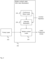
- FIG. 2 is a block diagram illustrating an embodiment of a mode-locked laser with gain modulation.
- mode-locked laser with gain modulation 200 comprises a system for optical comb carrier envelope offset frequency control.
- mode-locked laser with gain modulation 200 comprises mode-locked laser 204.
- mode-locked laser 204 comprises a fiber laser.
- Mode-locked laser 204 is pumped by pump laser 202.
- pump laser 202 comprises a laser diode, a gas laser, a solid-state laser, or any other appropriate laser type.
- Mode-locked laser with gain modulation 200 additionally comprises continuous wave laser 206 and intensity modulator 208.
- continuous wave laser 206 comprises a gas laser, a solid-state laser, a semiconductor laser, a laser diode, a dye laser, or any other appropriate laser type.
- intensity modulator 208 comprises a laser power attenuator, a laser power amplifier, an acousto-optic modulator, an electro-absorptive modulator, an electro-optic Mach-Zehnder intensity modulator, or any other appropriate intensity modulator.
- continuous wave laser 206 and intensity modulator 208 are integrated to form an intensity modulated continuous wave laser (e.g., a diode laser with an integrated modulator, a diode laser with distributed feedback, a distributed Bragg reflector laser, etc.).
- Continuous wave laser 206 and/or intensity modulator 208 are controlled by one or more control signals.
- intensity modulated continuous wave laser light couples into a laser cavity of mode-locked laser 204.
- intensity modulated continuous wave laser light affects a gain medium within the laser cavity of mode-locked laser 204.
- Figure 3 is a block diagram illustrating an embodiment of a mode-locked laser.
- mode-locked laser 300 comprises mode-locked laser 204 of Figure 2 .
- mode-locked laser 300 comprises a fiber laser.
- mode-locked laser with loss modulation 300 comprises a ring laser cavity.
- Mode-locked laser 300 comprises a set of elements coupled into a loop using optical fibers (e.g., optical fiber 310).
- Input output coupler 302 comprises an input output coupler for coupling input light (e.g., pump laser light, e.g., from pump laser 202 of Figure 2 ) into the fiber loop and for coupling output light (e.g., the output laser frequency comb) out from the fiber loop.
- input light e.g., pump laser light, e.g., from pump laser 202 of Figure 2
- output light e.g., the output laser frequency comb
- input output coupler 302 comprises a beam splitter (e.g., using a wavelength division multiplexer (WDM) tap isolator, a circulator, etc.).
- Gain fiber 306 comprises a gain medium for providing optical signal gain.
- gain fiber 306 comprises a rare-earth element doped gain medium (e.g., an erbium-doped gain medium, an ytterbium-doped gain medium, an erbium-ytterbium codoped gain medium, etc.).
- Mode-locker 308 comprises a mode-locker for shaping an optical pulse.
- mode-locker 308 comprises a passive mode-locker, a saturable absorber, a saturable absorber mirror, a semiconductor saturable absorber mirror (SESAM), a nonlinear loop mirror, Kerr lensing, nonlinear polarization rotation, or any other appropriate mode-locker.
- Input coupler 304 comprises an input coupler for coupling modulated continuous wave laser light into the fiber laser prior to the gain fiber.
- input coupler 304 comprises an optical circulator.
- the input coupler 304 is an optical circulator external to the laser cavity.
- modulated continuous wave laser light comprises modulated light from a continuous wave laser (e.g., continuous wave laser 206 of Figure 2 ).
- modulated continuous wave laser light affects gain fiber 306 (e.g., modulated continuous wave laser light depletes excited states of the gain medium).
- mode-locked laser 300 is implemented using a laser cavity configuration other than a ring cavity as shown in Figure 3 - for example, a linear cavity, a figure 8 cavity, a sigma cavity, etc.
- Figure 4 is a block diagram illustrating an embodiment of a mode-locked laser with closed-loop gain modulation.
- mode-locked laser with closed-loop gain modulation 400 comprises mode-locked laser with gain modulation 200 of Figure 2 additionally comprising a feedback loop.
- mode-locked laser with closed loop gain modulation 400 comprises a system for optical comb carrier envelope offset frequency control.
- mode-locked laser with closed-loop gain modulation 400 comprises mode-locked laser 404.
- Mode-locked laser 404 is pumped by pump laser 402.
- Mode-locked laser with gain modulation 200 additionally comprises continuous wave laser 406 and intensity modulator 408.
- intensity modulator 408 comprises an intensity modulator external to the laser cavity.
- continuous wave laser 406 and intensity modulator 408 are integrated to form an intensity modulated continuous wave laser.
- Continuous wave laser 406 and/or intensity modulator 408 are controlled by one or more control signals.
- intensity modulated continuous wave laser light couples into a laser cavity of mode-locked laser 404.
- intensity modulated continuous wave laser light affects a gain medium within the laser cavity of mode-locked laser 404.
- continuous wave laser 406 is one of the followings: a pulse laser, an LED, a part of the laser frequency comb, or any other appropriate source.
- the laser frequency comb output by frequency shifter 404 is split by beam splitter 414.
- a portion of the light is output as the mode-locked laser frequency comb output with closed-loop gain modulation, and a portion of the light is provided to beat note generator 410 for creation of a feedback control signal.
- beat note generator 410 comprises a beat note generator for extracting a carrier envelope offset frequency from a laser frequency comb.
- beat note generator 410 extracts a carrier envelope offset frequency from a laser frequency comb by comparing the laser frequency comb with a frequency doubled version of itself.
- the light from the original laser frequency comb and a frequency doubled version of itself are combined using a beam splitter combiner.
- the combiner comprises guiding the combined light onto the same spot on a photodiode.
- the photodiode converts the optical intensity beatnote into an electrical signal at the carrier envelope offset frequency.
- the carrier envelope offset frequency is provided to gain control signal generator 412.
- Gain control signal generator 412 receives the carrier envelope offset frequency and a reference frequency comprising the desired carrier envelope offset frequency and generates a control signal for providing to continuous wave laser 406 and/or intensity modulator 408 in order to stabilize the carrier envelope offset frequency to a controlled carrier envelope offset frequency.
- the control signal generator 412 comprises a phase-locked loop.
- a phase error detector is used to produce an output signal related to the phase difference between the input signals.
- a filter is used to filter the phase error detector output.
- the filter comprises a filter for stabilizing a control loop.
- the filter comprises a servo control filter that includes gain.
- gain control signal generator 412 creates more than one control signal (e.g., two control signals, three control signals, etc.).
- gain control signal generator 412 additionally produces a control signal for controlling pump laser 402 for mode locked laser 404. Since the carrier envelope frequency is controlled via depletion of the upper-state population in the gain medium, the actuation bandwidth is limited by the upper-state lifetime. In some embodiments, where an erbium fiber mode-locked laser is used, the bandwidth can be limited by a 10-30 kHz pole in the transfer function depending on the laser parameters. In order to combat the roll-off in the actuator, the transfer function of the servo loop filter is constructed with several lead stages (derivative paths) in order to extend the gain and phase margin of the control loop.
- the zero of the first lead stage is chosen at the same frequency as the pole in the gain modulation transfer function, while the frequency of the pole of the second lead stage is chosen an order of magnitude larger in frequency.
- the bandwidth of the control loop can be extended to in excess of 500 kHz.
- Figure 5 is a block diagram illustrating an embodiment of a mode-locked laser with loss modulation.
- mode-locked laser 500 comprises mode-locked laser 204 of Figure 2 .
- mode-locked laser with loss modulation 500 comprises a system for optical comb carrier envelope offset frequency control.
- mode-locked laser with loss modulation 500 comprises a fiber laser.
- mode-locked laser with loss modulation 500 comprises a ring laser cavity.
- Mode-locked laser with loss modulation 500 comprises a set of elements coupled into a loop using optical fibers (e.g., optical fiber 512).
- Input output coupler 504 comprises an input output coupler for coupling input light (e.g., pump laser light from pump laser 502) into the fiber loop and for coupling output light (e.g., the output laser frequency comb) out from the fiber loop.
- input output coupler 504 comprises a beam splitter (e.g., using a wavelength division multiplexer (WDM) tap isolator, a circulator, etc.).
- Gain fiber 506 comprises a gain fiber for providing optical signal gain.
- gain fiber 506 comprises a rare-earth element (e.g., erbium, ytterbium, thulium, etc.) doped fiber.
- Mode-locker 508 comprises a mode-locker for shaping an optical pulse.
- mode-locker 508 comprises a passive mode-locker, a saturable absorber, a saturable absorber mirror, a semiconductor saturable absorber mirror (SESAM), a nonlinear loop mirror, Kerr lensing, nonlinear polarization rotation, or any other appropriate mode-locker.
- Loss modulator 510 comprises a loss modulator for modulating a laser pulse. In some embodiments, loss modulator 510 comprises a controllable optical attenuator. In all embodiments, loss modulator 510 comprises a Mach-Zehnder intensity modulator.
- mode-locked laser with modulation 500 is implemented using a laser cavity configuration other than a ring cavity as shown in Figure 5 - for example, a linear cavity, a figure 8 cavity, a sigma cavity, etc.
- Figure 6 is a block diagram illustrating an embodiment of a loss modulator.
- loss modulator 600 comprises loss modulator 510 of Figure 5 .
- loss modulator 600 comprises a Mach-Zehnder intensity modulator.
- loss modulator 600 comprises a fiber-coupled waveguide modulator.
- loss modulator 600 comprises a dual-drive intensity modulator (e.g. z-cut LiNbO 3 crystal with independent drive for each waveguide, etc.); in this case, to make the device be zero-chirp, two signals that are out of phase must be fed to each drive.
- dual-drive intensity modulator e.g. z-cut LiNbO 3 crystal with independent drive for each waveguide, etc.
- loss modulator 600 comprises a zero-chirp modulator (e.g., a LiNbO 3 crystal with push-pull electrodes, a cross-cut LiNbO 3 crystal, etc.).
- a zero-chirp modulator e.g., a LiNbO 3 crystal with push-pull electrodes, a cross-cut LiNbO 3 crystal, etc.
- light enters optical waveguide 602, splits to follow an upper path and a lower path, and recombines on an exit path to exit the waveguide.
- Electrode 604 and electrode 606 are held at ground potential, and control voltages are applied to electrode 608 and electrode 610.
- Electrode 608 comprises a high frequency response control voltage (e.g., a fast modulation control signal) and electrode 610 comprises a low frequency response control voltage (e.g., a slow control signal for an intensity set point, wherein the intensity set point controls a mean value of the controlled carrier envelope offset frequency, as well as the sensitivity of the modulator (% loss per volt))
- a control signal applied to electrode 608 or electrode 610 causes a differential phase shift between the upper path and the lower path, causing destructive interference when the paths recombine.
- electrode 612 is held at ground potential and a phase control voltage is applied to electrode 614.
- electrode 614 and electrode 612 comprise an integrated waveguide phase modulator to control laser cavity length.
- loss modulator 600 does not include electrode 612 and electrode 614.
- loss modulator 600 comprises one set of electrodes (for example, electrode 608 and electrode 610 are combined into a single electrode).
- the one set of electrodes comprises a high frequency response control voltage and a low frequency response control voltage (e.g., a fast modulation control signal and a slow control signal for an intensity set point that are electrically combined).
- a fast modulation control signal and a slow control signal are electrically combined using a bias tree and/or a summing amplifier.
- Figure 7 is a block diagram illustrating an embodiment of a mode-locked laser with closed-loop loss modulation.
- mode-locked laser with closed-loop loss modulation 700 comprises mode-locked laser with loss modulation 500 of Figure 5 additionally comprising a feedback loop.
- mode-locked laser with closed loop loss modulation 700 comprises a system for optical comb carrier envelope offset frequency control.
- mode-locked laser with closed-loop loss modulation 700 comprises a fiber laser.
- Mode-locked laser with closed-loop loss modulation 700 comprises a set of elements coupled into a loop using optical fibers (e.g., optical fiber 718).
- Input output coupler 704 comprises an input output coupler for coupling input light (e.g., pump laser light from pump laser 702) into the fiber loop and for coupling output light (e.g., the output laser frequency comb) out from the fiber loop.
- input output coupler 704 comprises a beam splitter (e.g., using a wavelength division multiplexer (WDM) tap isolator, a circulator, etc.).
- WDM wavelength division multiplexer
- Gain fiber 706 comprises a gain fiber for providing optical signal gain.
- Mode-locker 708 comprises a mode-locker for shaping an optical pulse.
- Loss modulator 710 comprises a loss modulator for modulating a laser pulse.
- the loss modulator 710 comprises a Mach-Zehnder intensity modulator.
- photodetector 720 located after beamsplitter 718 is used to measure the mode-locked laser output intensity.
- mode-locked laser is implemented using a laser cavity configuration other than the ring cavity of shown in Figure 7 - for example, a linear cavity, a figure 8 cavity, a sigma cavity, etc.
- the laser frequency comb output from input output coupler 704 is split by beam splitter 716.
- a portion of the light is output as the mode-locked laser frequency comb output with closed-loop loss modulation, and a portion of the light is provided to beat note generator 712 for creation of a feedback control signal.
- beat note generator 712 comprises a beat note generator for extracting a carrier envelope offset frequency from a laser frequency comb.
- beat note generator 712 extracts a carrier envelope offset frequency from a laser frequency comb by comparing the laser frequency comb with a frequency doubled version of itself.
- the carrier envelope offset frequency is provided to loss control signal generator 714.
- the laser intensity measured by photodetector 720 is also provided to loss control signal generator 714.
- Loss control signal generator 714 receives the carrier envelope offset frequency and a reference frequency comprising the desired carrier envelope offset frequency and generates a control signal for providing to loss modulator 710 in order to stabilize the carrier envelope offset frequency to a controlled carrier envelope offset frequency.
- loss control signal generator 714 creates more than one control signal (e.g., two control signals, three control signals, etc.).
- control signal of the electrodes 610 is a low-pass filtered version of the control signal applied to electrodes 608.
- loss control signal generator 714 is used in a phase-locked loop. In some embodiments, loss control signal generator 714 additionally produces a control signal for controlling pump laser 702 for mode locked laser with closed-loop loss modulation 700.
- FIG 8 is a block diagram illustrating an embodiment of a beat note generator.
- beat note generator 800 comprises beat note generator 712 of Figure 7 .
- incoming laser light received by beat note generator 800 is split by beam splitter 812.
- a portion of the incoming light is received by spectrum extender 802 and a portion of the incoming light is received by frequency doubler 804.
- Spectrum extender 802 comprises a spectrum extending optical element (e.g., a nonlinear fiber, a photonic crystal fiber) for increasing the light intensity at higher frequencies.
- the laser light intensity at higher frequencies is already high enough and spectrum extender 802 is not used.
- Frequency doubler 804 comprises a frequency doubler (e.g., a frequency doubling crystal) for doubling the light frequency (e.g., without changing the envelope frequency, thus doubling the carrier envelope offset frequency).
- a frequency doubler e.g., a frequency doubling crystal
- Light from spectrum extender 802 and frequency doubler 804 is combined using combiner 806.
- combiner 806 comprises a beam splitter combiner.
- combiner 806 comprises guiding light from spectrum extender 802 and frequency doubler 804 onto the same spot on photodiode 808.
- Photodiode 808 comprises a photodiode for converting a light intensity into an electrical signal.
- the lowest frequency component comprises a beat note at the carrier envelope offset frequency.
- Higher frequency components are removed by filter 810 and a beat note output is created comprising the carrier envelope offset frequency.
- the beat note generator generates the beat note by determining a frequency difference between a spectrum extended version of the frequency shifted laser output and a frequency doubled version of the frequency shifted laser output.
- the beat note generator generates the beat note by determining a frequency difference between the frequency shifted laser output and a frequency doubled version of the frequency shifted laser output.
- FIG 9 is a block diagram illustrating an embodiment of a control signal generator.
- control signal generator 900 comprises gain control signal generator 412 of Figure 4 or loss control signal generator 714 of Figure 7 .
- control signal generator 900 is used in a phase-locked loop.
- control signal generator 900 receives a reference frequency comprising a desired carrier envelope offset frequency and a beat note comprising a measured carrier envelope offset frequency.
- Phase error detector 902 comprises a phase error detector for producing an output signal related to the phase difference between the input signals.
- phase error detector 902 comprises a phase/frequency error detector.
- Filter 904 comprises a filter for filtering the phase error detector output.
- filter 904 comprises a filter for stabilizing a control loop.
- filter 904 comprises a servo control filter that includes gain. In some embodiments, filter 904 also receives a reference voltage from the intensity photodetector (e.g., photodetector 720 of Figure 7 ). Filter 904 produces one or more signals for controlling a modulator (e.g., intensity modulator 408 of Figure 4 , loss modulator 710 of Figure 7 ) or a pump laser (e.g., pump laser 402 of Figure 4 or pump laser 702 of Figure 7 ). In the example shown, control signal generator 900 of Figure 9 produces a DC (e.g., direct current) control signal.
- DC direct current
- Figure 10 is a flow diagram illustrating an embodiment of a process for optical comb carrier envelope offset frequency control.
- the process of Figure 10 is executed by mode-locked laser with closed loop loss modulation 700 of Figure 7 .
- production of an output beam is caused using an input pump beam and one or more control signals, wherein the output beam includes a controlled carrier envelope offset frequency.
- production of a beat note signal using a portion of the output beam is caused.
- production of the one more control signals to set the beat note signal by modulating the intensity within the mode-locked oscillator is caused, wherein modulating the intensity includes using a Mach-Zehnder intensity modulator.
- the mode-locked laser output, the intensity modulator, the optical beat note generator, and pump laser modules are disposed so that carrier envelope offset frequency is controlled. In some embodiments, the mode-locked laser output, the intensity modulator, the optical beat note generator, and pump laser modules are fiber coupled.
- Figure 11 is a flow diagram illustrating an embodiment of a process for optical comb carrier envelope offset frequency control.
- the process of Figure 11 is executed by mode-locked laser with closed loop gain modulation 400 of Figure 4 .
- production of an output beam is caused using an input pump beam and one or more control signals, wherein the output beam includes a controlled carrier envelope offset frequency.
- production of a beat note signal using a portion of the output beam is caused.
- production of the one more control signals to set the beat note signal by modulating the intensity within the mode-locked oscillator is caused, wherein modulating the intensity includes using an intensity modulated laser to affect a gain medium within the mode-locked laser.
- the mode-locked laser output, the intensity modulator, the optical beat note generator, and pump laser modules are disposed so that carrier envelope offset frequency is controlled. In some embodiments, the mode-locked laser output, the intensity modulator, the optical beat note generator, and pump laser modules are fiber coupled.
Landscapes
- Physics & Mathematics (AREA)
- Electromagnetism (AREA)
- Nonlinear Science (AREA)
- Optics & Photonics (AREA)
- Engineering & Computer Science (AREA)
- Plasma & Fusion (AREA)
- General Physics & Mathematics (AREA)
- Chemical & Material Sciences (AREA)
- Crystallography & Structural Chemistry (AREA)
- Optical Modulation, Optical Deflection, Nonlinear Optics, Optical Demodulation, Optical Logic Elements (AREA)
- Lasers (AREA)
Claims (9)
- Modengekoppelter Laser mit Closed-Loop-Verlustmodulationssystem (700) mit optischer Kammträgerhüllkurven-Versatzfrequenzregelung, der Folgendes umfasst:einen modengekoppelten Oszillator, der einen Ringhohlraum mit einer Verstärkungsfaser (706) und einem Modenkoppler (708) umfasst, wobei der modengekoppelte Oszillator einen Ausgangsstrahl mittels eines von einem Pumplaser (702) bereitgestellten Pumpstrahls und eines oder mehrerer Steuersignale erzeugt, und wobei der Ausgangsstrahl eine gesteuerte Trägerhüllkurven-Versatzfrequenz umfasst;wobei die genannten ein oder mehreren Steuersignale von einem Schwebungsgenerator (712) erzeugt werden, wobei der Schwebungsgenerator ein Schwebungssignal unter Verwendung eines Teils des Ausgangsstrahls erzeugt; undeinen Steuersignalgenerator (714), wobei der Steuersignalgenerator die ein oder mehreren Steuersignale erzeugt, um das Schwebungssignal durch Modulieren der Intensität innerhalb des modengekoppelten Oszillators einzustellen, und wobei das Modulieren der Intensität die Verwendung eines Mach-Zehnder-Intensitätsverlustmodulators (710) beinhaltet, wobei sich der Mach-Zehnder-Intensitätsmodulator innerhalb des Ringhohlraums befindet.
- System nach Anspruch 1, wobei der Mach-Zehnder-Intensitätsmodulator einen fasergekoppelten Wellenleitermodulator oder einen Doppelantriebsmodulator mit unabhängigen Elektroden für jeden Arm des Wellenleiterinterferometers umfasst.
- System nach Anspruch 1, wobei der Mach-Zehnder-Intensitätsmodulator einen Null-Chirp-Modulator umfasst.
- System nach Anspruch 3, wobei der Null-Chirp-Modulator einen LiNbO3-Kristall mit Push-Pull-Elektroden umfasst.
- System nach Anspruch 1, wobei der Mach-Zehnder-Intensitätsmodulator mittels der ein oder mehreren Steuersignale gesteuert wird.
- System nach Anspruch 4, wobei der Mach-Zehnder-Intensitätsmodulator zwei Sätze von Elektroden (604, 606, 608, 610) umfasst, und wobei ein erster Satz von Elektroden der zwei Sätze von Elektroden für ein schnelles Modulationssteuersignal und ein zweiter Satz von Elektroden der zwei Sätze von Elektroden für ein langsames Steuersignal für einen Intensitätssollwert vorgesehen ist, wobei der Intensitätssollwert einen Mittelwert der gesteuerten Trägerhüllkurven-Versatzfrequenz regelt; und
wobei optional das schnelle Modulationssteuersignal und das langsame Steuersignal mittels eines Bias-Baums oder eines schnellen Summierverstärkers elektrisch kombiniert werden. - System nach Anspruch 4, wobei der Mach-Zehnder-Intensitätsmodulator einen Satz von Elektroden (608, 610) umfasst, wobei der eine Satz von Elektroden ein schnelles Modulationssteuersignal und ein langsames Steuersignal für einen Intensitätssollwert umfasst, die elektrisch kombiniert werden.
- System nach Anspruch 1, wobei dem Mach-Zehnder-Intensitätsmodulator ein integrierter Wellenleiter-Phasenmodulator (612, 614) folgt, um die Länge des Laserresonators zu regeln; oder wobei optional der modengekoppelte Oszillator eines der folgenden für Modenkopplung verwendet: einen sättigbaren Absorber, einen sättigbaren Absorberspiegel, einen sättigbaren Halbleiterabsorberspiegel, einen nichtlinearen Loop-Mirror, Kerr-Linsen oder nichtlineare Polarisationsrotation; oder wobei optional der modengekoppelte Oszillator mit einem Ringlaserresonator implementiert ist.
- Verfahren zur optischen Kammträgerhüllkurven-Versatzfrequenzregelung unter Verwendung einer Vorrichtung nach Anspruch 1, das Folgendes beinhaltet:Veranlassen (1000) der Erzeugung eines Ausgangsstrahls mittels eines Eingangspumpstrahls und eines oder mehrerer Steuersignale, wobei der Ausgangsstrahl eine gesteuerte Trägerhüllkurven-Versatzfrequenz umfasst;Veranlassen (1002) der Erzeugung eines Schwebungssignals anhand eines Teils des Ausgangsstrahls; undVeranlassen (1004) der Erzeugung der ein oder mehreren Steuersignale, um das Schwebungssignal durch Modulieren der Intensität innerhalb des modengekoppelten Oszillators einzustellen, wobei das Modulieren der Intensität die Verwendung eines Mach-Zehnder-Intensitätsmodulators beinhaltet, wobei der Mach-Zehnder-Intensitätsmodulator innerhalb des modengekoppelten Oszillators ist.
Applications Claiming Priority (3)
| Application Number | Priority Date | Filing Date | Title |
|---|---|---|---|
| US201662308155P | 2016-03-14 | 2016-03-14 | |
| US15/457,929 US10824047B2 (en) | 2016-03-14 | 2017-03-13 | Optical comb carrier envelope-offset frequency control using intensity modulation |
| PCT/US2017/022253 WO2017160802A1 (en) | 2016-03-14 | 2017-03-14 | Optical comb carrier envelope-offset frequency control using intensity modulation |
Publications (3)
| Publication Number | Publication Date |
|---|---|
| EP3430471A1 EP3430471A1 (de) | 2019-01-23 |
| EP3430471A4 EP3430471A4 (de) | 2020-01-22 |
| EP3430471B1 true EP3430471B1 (de) | 2023-06-28 |
Family
ID=59786481
Family Applications (1)
| Application Number | Title | Priority Date | Filing Date |
|---|---|---|---|
| EP17767313.4A Active EP3430471B1 (de) | 2016-03-14 | 2017-03-14 | Hüllenversatzfrequenzsteuerung mit intensitätsmodulation eines optischen kammträgers |
Country Status (3)
| Country | Link |
|---|---|
| US (2) | US10824047B2 (de) |
| EP (1) | EP3430471B1 (de) |
| WO (2) | WO2017160802A1 (de) |
Families Citing this family (21)
| Publication number | Priority date | Publication date | Assignee | Title |
|---|---|---|---|---|
| US10557880B2 (en) * | 2017-09-01 | 2020-02-11 | X Development Llc | Modelocked laser electric field sensor |
| US10649019B2 (en) | 2017-09-01 | 2020-05-12 | X Development Llc | Optically probed multi-element electric field sensing system |
| GB2567470B (en) * | 2017-10-13 | 2022-03-09 | M Squared Lasers Ltd | A laser system comprising two phase-locked continuous-wave laser sources |
| FR3074371B1 (fr) * | 2017-11-24 | 2021-05-14 | Ixblue | Dispositif et procede d'interaction entre un faisceau laser agile et une transition energetique hyperfine d'une espece chimique |
| CN107942450B (zh) * | 2017-11-28 | 2019-05-31 | 中南大学 | 一种耦合封装硅光子芯片 |
| EP3518354A1 (de) | 2018-01-25 | 2019-07-31 | Max-Planck-Gesellschaft zur Förderung der Wissenschaften e.V. | Vorrichtung und verfahren zur erzeugung von laserpulsen durch kerr-linsenbasierte modenkopplung mit einer verlustmodulationsvorrichtung als kerr-medium |
| CN109361146A (zh) * | 2018-12-24 | 2019-02-19 | 光越科技(深圳)有限公司 | 基于单片机反馈调节的超短脉冲光纤激光器种子源系统 |
| US11670905B2 (en) * | 2019-03-05 | 2023-06-06 | Nlight, Inc. | Methods to maintain and control the polarization state from 3C optical fiber |
| KR102191987B1 (ko) * | 2019-04-18 | 2020-12-16 | 한국과학기술연구원 | 그래핀을 이용하여 레이저의 잡음을 감소하기 위한 광소자 |
| CN110535019A (zh) * | 2019-08-30 | 2019-12-03 | 中国空间技术研究院 | 基于电光相位调制频移反馈环路的双脉冲激光产生方法 |
| CN111129936B (zh) * | 2019-12-13 | 2021-04-02 | 北京无线电计量测试研究所 | 一种锁模脉冲激光的产生装置及方法 |
| US12080988B2 (en) * | 2020-02-24 | 2024-09-03 | The Regents Of The University Of Colorado, A Body Corporate | Photonic-based microwave generator and associated methods |
| WO2022099112A1 (en) * | 2020-11-06 | 2022-05-12 | Government Of The United States Of America, As Represented By The Secretary Of Commerce | Direct digital chirp synthesizer and generating a chirped optical frequency comb |
| JP7811761B2 (ja) * | 2020-12-04 | 2026-02-06 | パナソニックホールディングス株式会社 | 光周波数コム装置および計測装置 |
| CN113300203B (zh) * | 2021-07-26 | 2021-10-08 | 济南量子技术研究院 | 一种光频梳的快速锁模方法及系统 |
| CN114205003B (zh) * | 2021-12-09 | 2023-10-20 | 北京邮电大学 | 一种用于过光纤链路的信号光与本振光频差信号锁定的快慢环结合反馈控制系统与方法 |
| CN114421261B (zh) * | 2021-12-31 | 2025-09-26 | 河南省启封新源光电科技有限公司 | 一种高速机械式脉冲激光调制器及调制方法 |
| CN114414993B (zh) * | 2022-01-19 | 2023-07-14 | 电子科技大学 | 一种电光强度调制器芯片频率响应测试的方法 |
| CN115149386B (zh) * | 2022-07-11 | 2024-01-12 | 中国科学院精密测量科学与技术创新研究院 | 一种基于fpga的激光频率稳定自动控制系统 |
| US12107380B1 (en) * | 2023-10-03 | 2024-10-01 | Vector Atomic, Inc. | Controlling soliton self-frequency shift |
| CN119805902B (zh) * | 2024-12-30 | 2025-10-31 | 西安空间无线电技术研究所 | 一种基于高速伪码的激光时间传递系统及方法 |
Family Cites Families (23)
| Publication number | Priority date | Publication date | Assignee | Title |
|---|---|---|---|---|
| US5745284A (en) * | 1996-02-23 | 1998-04-28 | President And Fellows Of Harvard College | Solid-state laser source of tunable narrow-bandwidth ultraviolet radiation |
| US7190705B2 (en) | 2000-05-23 | 2007-03-13 | Imra America. Inc. | Pulsed laser sources |
| US6847484B2 (en) | 2001-03-15 | 2005-01-25 | Jay N. Damask | Methods and apparatus for generating polarization mode dispersion |
| US7505196B2 (en) | 2004-03-31 | 2009-03-17 | Imra America, Inc. | Method and apparatus for controlling and protecting pulsed high power fiber amplifier systems |
| US7408693B2 (en) | 2004-07-27 | 2008-08-05 | Jds Uniphase Corporation | Electro-optic device |
| US7522642B2 (en) | 2006-03-29 | 2009-04-21 | Amo Development Llc | Method and system for laser amplification using a dual crystal Pockels cell |
| EP2040117A4 (de) | 2006-07-11 | 2009-09-30 | Japan Science & Tech Agency | Vorrichtung und verfahren zur erzeugung von synchronisierten optischen signalen |
| US8018979B2 (en) | 2007-10-04 | 2011-09-13 | Femtolasers Produktions Gmbh | Mode-locked short pulse laser resonator and short pulse laser arrangement |
| DE102010022585B4 (de) | 2010-06-03 | 2012-03-08 | Bundesrepublik Deutschland, vertreten durch das Bundesministerium für Wirtschaft und Technologie, dieses vertreten durch den Präsidenten der Physikalisch-Technischen Bundesanstalt | Verfahren zum Erzeugen von phasenkohärenten Lichtfeldern mit vorgebbarem Wert ihrer Frequenz und optischer Frequenz-Synthesizer |
| JP2014512019A (ja) * | 2011-03-14 | 2014-05-19 | イムラ アメリカ インコーポレイテッド | 光ファイバを用いた中赤外コヒーレント・コンティニュームの広帯域発生 |
| US9088371B2 (en) | 2011-04-30 | 2015-07-21 | Rwth Aachen | WDM telecommunications link with coherent detection and optical frequency comb sources |
| WO2012166572A1 (en) | 2011-05-27 | 2012-12-06 | Imra America, Inc. | Compact optical frequency comb systems |
| US8831056B2 (en) | 2011-06-30 | 2014-09-09 | Oewaves, Inc. | Compact optical atomic clocks and applications based on parametric nonlinear optical mixing in whispering gallery mode optical resonators |
| WO2013040168A2 (en) | 2011-09-14 | 2013-03-21 | The Massachusetts Institute Of Technology | Methods and apparatus for broadband frequency comb stabilization |
| EP2756342B1 (de) | 2011-09-14 | 2016-11-30 | IMRA America, Inc. | Steuerbare faserlaserquelle mit mehreren wellenlängen |
| US9019506B1 (en) | 2012-01-31 | 2015-04-28 | AOSense, Inc. | Phase control for dual atom interferometers |
| US9065242B2 (en) | 2012-05-17 | 2015-06-23 | The United States Of America As Represented By The Administrator Of The National Aeronautics Space Administration | Apparatus and method to enable precision and fast laser frequency tuning |
| US10018888B2 (en) * | 2012-06-06 | 2018-07-10 | Eospace, Inc. | Advanced techniques for improving high-efficiency optical modulators |
| WO2014107537A1 (en) | 2013-01-02 | 2014-07-10 | Packet Photonics, Inc. | Tunable u-laser transmitter with integrated mach-zehnder modulator |
| WO2015049106A2 (en) * | 2013-10-01 | 2015-04-09 | Université De Neuchâtel | Laser source |
| EP2866311B8 (de) | 2013-10-25 | 2018-06-27 | Ludwig-Maximilians-Universität München | Verfahren und Vorrichtung zur Steuerung einer Träger-Einhüllenden-Phase und/oder einer Intensität von Ausgangsimpulsen einer Impulslaservorrichtung |
| US9698913B2 (en) | 2014-06-06 | 2017-07-04 | The John Hopkins University | System and method for distortion correction in phase-encoded photonic links |
| JP6476648B2 (ja) | 2014-08-21 | 2019-03-06 | 住友電気工業株式会社 | マッハツェンダ変調器 |
-
2017
- 2017-03-13 US US15/457,929 patent/US10824047B2/en active Active
- 2017-03-13 US US15/457,928 patent/US9977311B2/en active Active
- 2017-03-14 EP EP17767313.4A patent/EP3430471B1/de active Active
- 2017-03-14 WO PCT/US2017/022253 patent/WO2017160802A1/en not_active Ceased
- 2017-03-14 WO PCT/US2017/022247 patent/WO2017160798A1/en not_active Ceased
Also Published As
| Publication number | Publication date |
|---|---|
| EP3430471A1 (de) | 2019-01-23 |
| US20170261832A1 (en) | 2017-09-14 |
| WO2017160802A1 (en) | 2017-09-21 |
| WO2017160798A1 (en) | 2017-09-21 |
| US10824047B2 (en) | 2020-11-03 |
| US20170264070A1 (en) | 2017-09-14 |
| US9977311B2 (en) | 2018-05-22 |
| EP3430471A4 (de) | 2020-01-22 |
Similar Documents
| Publication | Publication Date | Title |
|---|---|---|
| US10824047B2 (en) | Optical comb carrier envelope-offset frequency control using intensity modulation | |
| Wu et al. | High-repetition-rate optical pulse generation using a rational harmonic mode-locked fiber laser | |
| Wu et al. | Direct selection and amplification of individual narrowly spaced optical comb modes via injection locking: design and characterization | |
| US10859888B2 (en) | System for generating brief or ultra-brief light pulses | |
| US20100284430A1 (en) | Systems and methods for generating high repetition rate ultra-short optical pulses | |
| Haverkamp et al. | Frequency stabilization of mode-locked Erbium fiber lasers using pump power control | |
| GB2369486A (en) | A mode locked laser | |
| US9680287B2 (en) | Opto-optical modulation of a saturable absorber for high bandwidth CEO stabilization of a femtosecond laser frequency comb | |
| USH1926H (en) | Actively mode-locked, single-polarization, picosecond optical fiber laser | |
| JP2018139279A (ja) | 光ファイバーレーザー装置 | |
| JP2019179918A (ja) | スペクトル細分によるシングルレーザーキャビティからのデュアルコム生成 | |
| WO2019053487A1 (en) | LASER OR STABILIZED OPTICAL AMPLIFIER AND METHOD OF STABILIZATION | |
| Smirnov et al. | Shaping of nanosecond pulses in ytterbium fiber lasers by synchronous sine-wave pump modulation | |
| CN103178436B (zh) | 主动锁模激光器超模噪声抑制方法及装置 | |
| CN117120922A (zh) | 用于产生持续时间和/或重复频率可调的亚皮秒持续时间光脉冲的系统和方法 | |
| KR100545778B1 (ko) | 유리수차 조화 모드-잠김 반도체 광섬유 레이저 내에서의펄스 진폭 균등화 장치 및 방법 | |
| Yang et al. | Comparison on different repetition rate locking methods in Er-doped fiber laser | |
| JP2013025284A (ja) | 短パルス光発生装置および方法 | |
| Ramirez et al. | Regenerative multi-tone injection locking for linewidth enhancement and repetition rate stabilization of a PIC mode-locked laser | |
| Nyushkov et al. | Hybrid fiber laser integrating fast and slow active media for accurate synthesis of high-energy arbitrary optical waveforms by cavity dumping | |
| JPH02310982A (ja) | モード同期ファイバレーザ装置 | |
| Singh et al. | Mode-locking of fibre ring lasers with a coherent-phase relationship among axial mode groups | |
| Ramirez et al. | Optical linewidth and RF phase noise reduction of a chip-scale CPM laser using COEO multi-tone injection locking | |
| JPH03229478A (ja) | モード同期レーザ装置 | |
| US20250260208A1 (en) | Mode-locking method and system |
Legal Events
| Date | Code | Title | Description |
|---|---|---|---|
| STAA | Information on the status of an ep patent application or granted ep patent |
Free format text: STATUS: THE INTERNATIONAL PUBLICATION HAS BEEN MADE |
|
| PUAI | Public reference made under article 153(3) epc to a published international application that has entered the european phase |
Free format text: ORIGINAL CODE: 0009012 |
|
| STAA | Information on the status of an ep patent application or granted ep patent |
Free format text: STATUS: REQUEST FOR EXAMINATION WAS MADE |
|
| 17P | Request for examination filed |
Effective date: 20180813 |
|
| AK | Designated contracting states |
Kind code of ref document: A1 Designated state(s): AL AT BE BG CH CY CZ DE DK EE ES FI FR GB GR HR HU IE IS IT LI LT LU LV MC MK MT NL NO PL PT RO RS SE SI SK SM TR |
|
| AX | Request for extension of the european patent |
Extension state: BA ME |
|
| RIN1 | Information on inventor provided before grant (corrected) |
Inventor name: CINGOZ, ARMAN Inventor name: ZHU, MIAO Inventor name: CHURIN, DMITRIY Inventor name: ROSLUND, JONATHAN |
|
| DAV | Request for validation of the european patent (deleted) | ||
| DAX | Request for extension of the european patent (deleted) | ||
| A4 | Supplementary search report drawn up and despatched |
Effective date: 20200102 |
|
| RIC1 | Information provided on ipc code assigned before grant |
Ipc: H04B 10/58 20130101ALI20191217BHEP Ipc: G04F 5/14 20060101ALI20191217BHEP Ipc: H03L 7/04 20060101ALI20191217BHEP Ipc: H04B 10/60 20130101ALI20191217BHEP Ipc: H04B 10/61 20130101ALI20191217BHEP Ipc: H03L 7/02 20060101ALI20191217BHEP Ipc: G02F 1/21 20060101AFI20191217BHEP Ipc: H04B 10/64 20130101ALI20191217BHEP Ipc: H01S 3/10 20060101ALI20191217BHEP |
|
| GRAP | Despatch of communication of intention to grant a patent |
Free format text: ORIGINAL CODE: EPIDOSNIGR1 |
|
| STAA | Information on the status of an ep patent application or granted ep patent |
Free format text: STATUS: GRANT OF PATENT IS INTENDED |
|
| INTG | Intention to grant announced |
Effective date: 20230320 |
|
| GRAS | Grant fee paid |
Free format text: ORIGINAL CODE: EPIDOSNIGR3 |
|
| GRAA | (expected) grant |
Free format text: ORIGINAL CODE: 0009210 |
|
| STAA | Information on the status of an ep patent application or granted ep patent |
Free format text: STATUS: THE PATENT HAS BEEN GRANTED |
|
| AK | Designated contracting states |
Kind code of ref document: B1 Designated state(s): AL AT BE BG CH CY CZ DE DK EE ES FI FR GB GR HR HU IE IS IT LI LT LU LV MC MK MT NL NO PL PT RO RS SE SI SK SM TR |
|
| REG | Reference to a national code |
Ref country code: CH Ref legal event code: EP |
|
| REG | Reference to a national code |
Ref country code: DE Ref legal event code: R081 Ref document number: 602017070688 Country of ref document: DE Owner name: AOSENSE, INC., FREMONT, US Free format text: FORMER OWNER: AOSENSE, INC., SUNNYVALE, CA, US |
|
| P01 | Opt-out of the competence of the unified patent court (upc) registered |
Effective date: 20230603 |
|
| REG | Reference to a national code |
Ref country code: AT Ref legal event code: REF Ref document number: 1583228 Country of ref document: AT Kind code of ref document: T Effective date: 20230715 |
|
| REG | Reference to a national code |
Ref country code: IE Ref legal event code: FG4D |
|
| REG | Reference to a national code |
Ref country code: DE Ref legal event code: R096 Ref document number: 602017070688 Country of ref document: DE |
|
| RAP4 | Party data changed (patent owner data changed or rights of a patent transferred) |
Owner name: AOSENSE, INC. |
|
| REG | Reference to a national code |
Ref country code: LT Ref legal event code: MG9D |
|
| PG25 | Lapsed in a contracting state [announced via postgrant information from national office to epo] |
Ref country code: SE Free format text: LAPSE BECAUSE OF FAILURE TO SUBMIT A TRANSLATION OF THE DESCRIPTION OR TO PAY THE FEE WITHIN THE PRESCRIBED TIME-LIMIT Effective date: 20230628 Ref country code: NO Free format text: LAPSE BECAUSE OF FAILURE TO SUBMIT A TRANSLATION OF THE DESCRIPTION OR TO PAY THE FEE WITHIN THE PRESCRIBED TIME-LIMIT Effective date: 20230928 |
|
| REG | Reference to a national code |
Ref country code: NL Ref legal event code: MP Effective date: 20230628 |
|
| REG | Reference to a national code |
Ref country code: AT Ref legal event code: MK05 Ref document number: 1583228 Country of ref document: AT Kind code of ref document: T Effective date: 20230628 |
|
| PG25 | Lapsed in a contracting state [announced via postgrant information from national office to epo] |
Ref country code: RS Free format text: LAPSE BECAUSE OF FAILURE TO SUBMIT A TRANSLATION OF THE DESCRIPTION OR TO PAY THE FEE WITHIN THE PRESCRIBED TIME-LIMIT Effective date: 20230628 Ref country code: NL Free format text: LAPSE BECAUSE OF FAILURE TO SUBMIT A TRANSLATION OF THE DESCRIPTION OR TO PAY THE FEE WITHIN THE PRESCRIBED TIME-LIMIT Effective date: 20230628 Ref country code: LV Free format text: LAPSE BECAUSE OF FAILURE TO SUBMIT A TRANSLATION OF THE DESCRIPTION OR TO PAY THE FEE WITHIN THE PRESCRIBED TIME-LIMIT Effective date: 20230628 Ref country code: LT Free format text: LAPSE BECAUSE OF FAILURE TO SUBMIT A TRANSLATION OF THE DESCRIPTION OR TO PAY THE FEE WITHIN THE PRESCRIBED TIME-LIMIT Effective date: 20230628 Ref country code: HR Free format text: LAPSE BECAUSE OF FAILURE TO SUBMIT A TRANSLATION OF THE DESCRIPTION OR TO PAY THE FEE WITHIN THE PRESCRIBED TIME-LIMIT Effective date: 20230628 Ref country code: GR Free format text: LAPSE BECAUSE OF FAILURE TO SUBMIT A TRANSLATION OF THE DESCRIPTION OR TO PAY THE FEE WITHIN THE PRESCRIBED TIME-LIMIT Effective date: 20230929 |
|
| PG25 | Lapsed in a contracting state [announced via postgrant information from national office to epo] |
Ref country code: FI Free format text: LAPSE BECAUSE OF FAILURE TO SUBMIT A TRANSLATION OF THE DESCRIPTION OR TO PAY THE FEE WITHIN THE PRESCRIBED TIME-LIMIT Effective date: 20230628 |
|
| PG25 | Lapsed in a contracting state [announced via postgrant information from national office to epo] |
Ref country code: SK Free format text: LAPSE BECAUSE OF FAILURE TO SUBMIT A TRANSLATION OF THE DESCRIPTION OR TO PAY THE FEE WITHIN THE PRESCRIBED TIME-LIMIT Effective date: 20230628 |
|
| PG25 | Lapsed in a contracting state [announced via postgrant information from national office to epo] |
Ref country code: ES Free format text: LAPSE BECAUSE OF FAILURE TO SUBMIT A TRANSLATION OF THE DESCRIPTION OR TO PAY THE FEE WITHIN THE PRESCRIBED TIME-LIMIT Effective date: 20230628 |
|
| PG25 | Lapsed in a contracting state [announced via postgrant information from national office to epo] |
Ref country code: IS Free format text: LAPSE BECAUSE OF FAILURE TO SUBMIT A TRANSLATION OF THE DESCRIPTION OR TO PAY THE FEE WITHIN THE PRESCRIBED TIME-LIMIT Effective date: 20231028 |
|
| PG25 | Lapsed in a contracting state [announced via postgrant information from national office to epo] |
Ref country code: SM Free format text: LAPSE BECAUSE OF FAILURE TO SUBMIT A TRANSLATION OF THE DESCRIPTION OR TO PAY THE FEE WITHIN THE PRESCRIBED TIME-LIMIT Effective date: 20230628 Ref country code: SK Free format text: LAPSE BECAUSE OF FAILURE TO SUBMIT A TRANSLATION OF THE DESCRIPTION OR TO PAY THE FEE WITHIN THE PRESCRIBED TIME-LIMIT Effective date: 20230628 Ref country code: RO Free format text: LAPSE BECAUSE OF FAILURE TO SUBMIT A TRANSLATION OF THE DESCRIPTION OR TO PAY THE FEE WITHIN THE PRESCRIBED TIME-LIMIT Effective date: 20230628 Ref country code: PT Free format text: LAPSE BECAUSE OF FAILURE TO SUBMIT A TRANSLATION OF THE DESCRIPTION OR TO PAY THE FEE WITHIN THE PRESCRIBED TIME-LIMIT Effective date: 20231030 Ref country code: IS Free format text: LAPSE BECAUSE OF FAILURE TO SUBMIT A TRANSLATION OF THE DESCRIPTION OR TO PAY THE FEE WITHIN THE PRESCRIBED TIME-LIMIT Effective date: 20231028 Ref country code: ES Free format text: LAPSE BECAUSE OF FAILURE TO SUBMIT A TRANSLATION OF THE DESCRIPTION OR TO PAY THE FEE WITHIN THE PRESCRIBED TIME-LIMIT Effective date: 20230628 Ref country code: EE Free format text: LAPSE BECAUSE OF FAILURE TO SUBMIT A TRANSLATION OF THE DESCRIPTION OR TO PAY THE FEE WITHIN THE PRESCRIBED TIME-LIMIT Effective date: 20230628 Ref country code: CZ Free format text: LAPSE BECAUSE OF FAILURE TO SUBMIT A TRANSLATION OF THE DESCRIPTION OR TO PAY THE FEE WITHIN THE PRESCRIBED TIME-LIMIT Effective date: 20230628 Ref country code: AT Free format text: LAPSE BECAUSE OF FAILURE TO SUBMIT A TRANSLATION OF THE DESCRIPTION OR TO PAY THE FEE WITHIN THE PRESCRIBED TIME-LIMIT Effective date: 20230628 |
|
| PG25 | Lapsed in a contracting state [announced via postgrant information from national office to epo] |
Ref country code: PL Free format text: LAPSE BECAUSE OF FAILURE TO SUBMIT A TRANSLATION OF THE DESCRIPTION OR TO PAY THE FEE WITHIN THE PRESCRIBED TIME-LIMIT Effective date: 20230628 |
|
| REG | Reference to a national code |
Ref country code: DE Ref legal event code: R097 Ref document number: 602017070688 Country of ref document: DE |
|
| PG25 | Lapsed in a contracting state [announced via postgrant information from national office to epo] |
Ref country code: DK Free format text: LAPSE BECAUSE OF FAILURE TO SUBMIT A TRANSLATION OF THE DESCRIPTION OR TO PAY THE FEE WITHIN THE PRESCRIBED TIME-LIMIT Effective date: 20230628 |
|
| PLBE | No opposition filed within time limit |
Free format text: ORIGINAL CODE: 0009261 |
|
| STAA | Information on the status of an ep patent application or granted ep patent |
Free format text: STATUS: NO OPPOSITION FILED WITHIN TIME LIMIT |
|
| PG25 | Lapsed in a contracting state [announced via postgrant information from national office to epo] |
Ref country code: IT Free format text: LAPSE BECAUSE OF FAILURE TO SUBMIT A TRANSLATION OF THE DESCRIPTION OR TO PAY THE FEE WITHIN THE PRESCRIBED TIME-LIMIT Effective date: 20230628 |
|
| 26N | No opposition filed |
Effective date: 20240402 |
|
| PG25 | Lapsed in a contracting state [announced via postgrant information from national office to epo] |
Ref country code: SI Free format text: LAPSE BECAUSE OF FAILURE TO SUBMIT A TRANSLATION OF THE DESCRIPTION OR TO PAY THE FEE WITHIN THE PRESCRIBED TIME-LIMIT Effective date: 20230628 |
|
| REG | Reference to a national code |
Ref country code: CH Ref legal event code: PL |
|
| PG25 | Lapsed in a contracting state [announced via postgrant information from national office to epo] |
Ref country code: BG Free format text: LAPSE BECAUSE OF FAILURE TO SUBMIT A TRANSLATION OF THE DESCRIPTION OR TO PAY THE FEE WITHIN THE PRESCRIBED TIME-LIMIT Effective date: 20230628 |
|
| PG25 | Lapsed in a contracting state [announced via postgrant information from national office to epo] |
Ref country code: LU Free format text: LAPSE BECAUSE OF NON-PAYMENT OF DUE FEES Effective date: 20240314 |
|
| PG25 | Lapsed in a contracting state [announced via postgrant information from national office to epo] |
Ref country code: MC Free format text: LAPSE BECAUSE OF FAILURE TO SUBMIT A TRANSLATION OF THE DESCRIPTION OR TO PAY THE FEE WITHIN THE PRESCRIBED TIME-LIMIT Effective date: 20230628 |
|
| PG25 | Lapsed in a contracting state [announced via postgrant information from national office to epo] |
Ref country code: MC Free format text: LAPSE BECAUSE OF FAILURE TO SUBMIT A TRANSLATION OF THE DESCRIPTION OR TO PAY THE FEE WITHIN THE PRESCRIBED TIME-LIMIT Effective date: 20230628 Ref country code: LU Free format text: LAPSE BECAUSE OF NON-PAYMENT OF DUE FEES Effective date: 20240314 Ref country code: BG Free format text: LAPSE BECAUSE OF FAILURE TO SUBMIT A TRANSLATION OF THE DESCRIPTION OR TO PAY THE FEE WITHIN THE PRESCRIBED TIME-LIMIT Effective date: 20230628 |
|
| REG | Reference to a national code |
Ref country code: BE Ref legal event code: MM Effective date: 20240331 |
|
| PG25 | Lapsed in a contracting state [announced via postgrant information from national office to epo] |
Ref country code: BE Free format text: LAPSE BECAUSE OF NON-PAYMENT OF DUE FEES Effective date: 20240331 |
|
| PG25 | Lapsed in a contracting state [announced via postgrant information from national office to epo] |
Ref country code: IE Free format text: LAPSE BECAUSE OF NON-PAYMENT OF DUE FEES Effective date: 20240314 |
|
| PG25 | Lapsed in a contracting state [announced via postgrant information from national office to epo] |
Ref country code: IE Free format text: LAPSE BECAUSE OF NON-PAYMENT OF DUE FEES Effective date: 20240314 Ref country code: BE Free format text: LAPSE BECAUSE OF NON-PAYMENT OF DUE FEES Effective date: 20240331 Ref country code: CH Free format text: LAPSE BECAUSE OF NON-PAYMENT OF DUE FEES Effective date: 20240331 |
|
| PG25 | Lapsed in a contracting state [announced via postgrant information from national office to epo] |
Ref country code: CY Free format text: LAPSE BECAUSE OF FAILURE TO SUBMIT A TRANSLATION OF THE DESCRIPTION OR TO PAY THE FEE WITHIN THE PRESCRIBED TIME-LIMIT; INVALID AB INITIO Effective date: 20170314 |
|
| PG25 | Lapsed in a contracting state [announced via postgrant information from national office to epo] |
Ref country code: HU Free format text: LAPSE BECAUSE OF FAILURE TO SUBMIT A TRANSLATION OF THE DESCRIPTION OR TO PAY THE FEE WITHIN THE PRESCRIBED TIME-LIMIT; INVALID AB INITIO Effective date: 20170314 |
|
| PG25 | Lapsed in a contracting state [announced via postgrant information from national office to epo] |
Ref country code: TR Free format text: LAPSE BECAUSE OF FAILURE TO SUBMIT A TRANSLATION OF THE DESCRIPTION OR TO PAY THE FEE WITHIN THE PRESCRIBED TIME-LIMIT Effective date: 20230628 |
|
| PGFP | Annual fee paid to national office [announced via postgrant information from national office to epo] |
Ref country code: GB Payment date: 20260219 Year of fee payment: 10 |
|
| PGFP | Annual fee paid to national office [announced via postgrant information from national office to epo] |
Ref country code: DE Payment date: 20260219 Year of fee payment: 10 |
|
| PGFP | Annual fee paid to national office [announced via postgrant information from national office to epo] |
Ref country code: FR Payment date: 20260220 Year of fee payment: 10 |