EP3432014A1 - Procédé et système d'entretien préventif des circuits intégrés - Google Patents
Procédé et système d'entretien préventif des circuits intégrés Download PDFInfo
- Publication number
- EP3432014A1 EP3432014A1 EP17182034.3A EP17182034A EP3432014A1 EP 3432014 A1 EP3432014 A1 EP 3432014A1 EP 17182034 A EP17182034 A EP 17182034A EP 3432014 A1 EP3432014 A1 EP 3432014A1
- Authority
- EP
- European Patent Office
- Prior art keywords
- electronic component
- propagation time
- signal propagation
- sensors
- values
- Prior art date
- Legal status (The legal status is an assumption and is not a legal conclusion. Google has not performed a legal analysis and makes no representation as to the accuracy of the status listed.)
- Withdrawn
Links
Images

Classifications
-
- G—PHYSICS
- G01—MEASURING; TESTING
- G01R—MEASURING ELECTRIC VARIABLES; MEASURING MAGNETIC VARIABLES
- G01R31/00—Arrangements for testing electric properties; Arrangements for locating electric faults; Arrangements for electrical testing characterised by what is being tested not provided for elsewhere
- G01R31/28—Testing of electronic circuits, e.g. by signal tracer
- G01R31/317—Testing of digital circuits
- G01R31/31725—Timing aspects, e.g. clock distribution, skew, propagation delay
-
- G—PHYSICS
- G01—MEASURING; TESTING
- G01K—MEASURING TEMPERATURE; MEASURING QUANTITY OF HEAT; THERMALLY-SENSITIVE ELEMENTS NOT OTHERWISE PROVIDED FOR
- G01K13/00—Thermometers specially adapted for specific purposes
-
- G—PHYSICS
- G01—MEASURING; TESTING
- G01R—MEASURING ELECTRIC VARIABLES; MEASURING MAGNETIC VARIABLES
- G01R31/00—Arrangements for testing electric properties; Arrangements for locating electric faults; Arrangements for electrical testing characterised by what is being tested not provided for elsewhere
- G01R31/28—Testing of electronic circuits, e.g. by signal tracer
- G01R31/2851—Testing of integrated circuits [IC]
- G01R31/2855—Environmental, reliability or burn-in testing
- G01R31/2856—Internal circuit aspects, e.g. built-in test features; Test chips; Measuring material aspects, e.g. electro migration [EM]
-
- G—PHYSICS
- G06—COMPUTING OR CALCULATING; COUNTING
- G06F—ELECTRIC DIGITAL DATA PROCESSING
- G06F11/00—Error detection; Error correction; Monitoring
-
- G—PHYSICS
- G01—MEASURING; TESTING
- G01K—MEASURING TEMPERATURE; MEASURING QUANTITY OF HEAT; THERMALLY-SENSITIVE ELEMENTS NOT OTHERWISE PROVIDED FOR
- G01K2217/00—Temperature measurement using electric or magnetic components already present in the system to be measured
-
- G—PHYSICS
- G01—MEASURING; TESTING
- G01R—MEASURING ELECTRIC VARIABLES; MEASURING MAGNETIC VARIABLES
- G01R31/00—Arrangements for testing electric properties; Arrangements for locating electric faults; Arrangements for electrical testing characterised by what is being tested not provided for elsewhere
- G01R31/28—Testing of electronic circuits, e.g. by signal tracer
- G01R31/2851—Testing of integrated circuits [IC]
- G01R31/2882—Testing timing characteristics
-
- G—PHYSICS
- G06—COMPUTING OR CALCULATING; COUNTING
- G06F—ELECTRIC DIGITAL DATA PROCESSING
- G06F2119/00—Details relating to the type or aim of the analysis or the optimisation
- G06F2119/04—Ageing analysis or optimisation against ageing
Definitions
- the present invention relates generally to the field of electronic systems and circuits, more particularly to integrated circuits such as e.g. Application Specific Integrated Circuits (ASICs) and Field Programmable Gate Arrays (FPGAs).
- ASICs Application Specific Integrated Circuits
- FPGAs Field Programmable Gate Arrays
- the present invention relates to a method for the predictive maintenance of an electronic component, which is designed as an integrated circuit, in particular as an ASIC or FPGA.
- This electronic component has sensors at at least one position, from which system parameters and a signal propagation time at the at least one position are determined during operation of the electronic component.
- the present invention also relates to an associated system for the predictive maintenance of an electronic component.
- the system reliability of the overall system is a key factor, especially in safety-critical applications.
- the system reliability of the overall system can in particular be strongly influenced by the lifetime of individual system components or assemblies or the underlying electronic components, wherein the life of a system component or an electronic component is usually referred to a time in which they are used without replacement or complete failure can.
- corresponding alarms can then be triggered and countermeasures can be taken in good time-ie before the failure of the respective system component or the overall system-such as, for example, timely maintenance and / or a timely replacement of the affected component.
- Methods of predictive maintenance for example, have been used for some time now in the field of aviation and space technology, for example for optimizing engine maintenance or the logistics required for this purpose.
- information is derived from a large number of existing sensor data from the engines, by means of which maintenance can be supported and optimized.
- An embedded system is an electronic system component (e.g., computer or computer) incorporated in a technical context, e.g. Monitoring, control and / or regulating functions takes over or e.g. is responsible for signal processing.
- Embedded systems are often adapted to the particular task and often have to meet real-time requirements.
- a malfunction or failure of an integrated circuit leads in many cases or almost always to a malfunction and as a result to a failure of the entire system and thus causes at least idle times.
- critical components which are often designed as integrated circuits such as ASICs or FPGAs, replaced in rather pessimistic - ie rather short-chosen - maintenance intervals. These maintenance intervals are very often determined by the electronic components designed as integrated circuits, in which malfunctions and / or fault conditions or failures can occur, in particular due to aging.
- Integrated circuits are usually electronic circuits which are deposited on a thin, usually a few millimeters thick die (die or die) of semiconductor material (e.g., silicon) and encased in a chip package for protection and easier contacting.
- the integrated circuit typically consists of a combination of numerous electrically connected electronic semiconductor devices (e.g., transistors, diodes, and / or other active and / or passive devices).
- electrically connected electronic semiconductor devices e.g., transistors, diodes, and / or other active and / or passive devices.
- the life of the respective electronic component or the respective integrated circuit can be used.
- ASIC application specific integrated circuit
- FPGA field-programmable gate array
- the manufacturer guarantees a maximum failure rate under certain conditions (eg temperature range for operation, maximum voltage, etc.). From a totality of the manufacturer's information for the respective individual electronic components or integrated circuits of the overall system, a service life and, as a result, a maintenance interval for the entire system can be derived.
- a disadvantage of this approach is that the manufacturer data such as e.g. the maximum failure rate, etc. for an integrated circuit is usually based on average or mean values of e.g. Reliability tests and / or stress tests at e.g. increased temperature and / or voltage, etc. are based. Therefore, no concrete assumptions can be made regarding the particular integrated circuits used in the overall system during operation.
- An integrated circuit can e.g. due to their use or operational range during operation have a slower or faster aging and thus a greater or lesser reliability or have a longer or shorter life than specified. On the one hand, this can be done especially with critical components, e.g. lead to relatively short maintenance intervals and / or any unnecessary or premature replacement of the electronic component and thus to additional costs.
- ASICs and / or FPGAs have to use predictive or predictive maintenance to detect malfunction / failure, fault conditions, and failures of electronic components early, especially due to aging.
- CMOS reliability challenges For example, a method for predicting integrated circuit failures, particularly based on CMOS technology, is known.
- CMOS reliability challenges For example, a method for predicting integrated circuit failures, particularly based on CMOS technology, is known.
- a large number of different sensors are attached to different positions in the semiconductor material or in the chip of an integrated circuit. From these sensors, information about various system parameters such as temperature, voltage, ring oscillator delay, complex, temporal relationships become more logical Signals, etc. collected.
- the information gathered by the sensors can then be evaluated on-chip or off-chip to identify abnormalities and predict any malfunction. Due to the large amount of information, however, this method requires a relative and possibly time-consuming and cost-intensive evaluation.
- the invention is therefore based on the object of specifying a method for the predictive maintenance of electronic components or of integrated circuits and an associated system for carrying out the method by which malfunctions and / or fault conditions of electronic components or with little effort and with little effort integrated circuits, in particular due to aging, can be detected early.
- the object is achieved by a method of the type mentioned, in which a central monitoring unit is mounted in the electronic component. From this central monitoring unit, the values of the system parameters, such as voltage and temperature, currently determined by the sensors in the electronic component at the at least one position and the currently determined signal propagation time at the at least one position are queried. On the basis of the currently determined values of the system parameters, the central monitoring unit determines a respectively valid limit value for the signal propagation time at the at least one position. The respective valid limit for the signal propagation time is compared with the currently determined value of the signal propagation time at the at least one position. When the respective valid limit value for the signal propagation time is exceeded by the currently determined value of the signal propagation time at the at least one position, a message is sent to a higher level by the central monitoring unit.
- the system parameters such as voltage and temperature
- the main aspect of the method according to the invention is that it can be recognized quickly, easily and with relatively little effort at an early stage that a malfunction and / or an error condition will occur in an electronic component in the near future.
- the method according to the invention not only saves costs, but also makes maintenance intervals better and / or more dynamic and demand-oriented, and reduces or partially eliminates downtimes.
- a significant deceleration of the signal propagation time can be determined very simply and rapidly. In the near future occurring malfunctions and fault conditions in electronic components or integrated circuits, which would occur due to aging, are thus detected early and can be reported to a higher level.
- Such a superordinate level can be, for example, an overall system in which the electronic component is installed, or a central control unit (for example for several complete systems).
- a maintenance of an entire system or an exchange of the affected system component in which the electronic component or the integrated circuit is used, or of the electronic component itself can be promptly initiated without, for example, causing it. to additional idle time comes.
- the sensors mounted in at least one position in the electronic component are combined in a position-specific manner in at least one monitoring element.
- the monitoring element bundles the sensors at a position of the electronic component or the values of the system parameters and the signal propagation time supplied by the sensors at this position, thereby simplifying their transmission to the central monitoring unit.
- integrated circuits which may have sensors for determining system parameters and the running time at a plurality of positions, by interrogating the sensors at the respective positions of the electronic component to monitoring elements, the query of the current values of the system parameters and the signal delay for the respective position for the central monitoring unit are considerably simplified.
- the respective position from which these values originate can be detected or determined by the central monitoring unit much more easily.
- the respectively determined, valid limit is ideally one specified tolerance or a specifiable guard interval below the critical value for the signal propagation time.
- the critical value for the signal propagation time depends on the particular application or on the respective use of the electronic component.
- the critical value indicates a signal transit time for the respective application, from which malfunction, fault conditions and / or failures will occur due to age-related signal delays and in which the electronic component must be replaced. Since the respectively determined, valid limit value for the signal propagation time is still below the critical value, for example the electronic component or the integrated circuit can be exchanged in good time - ie even before age-related malfunctions and / or fault conditions occur in the electronic, integrated component.
- the values of the system parameters and the signal propagation time currently determined by the sensors at the at least one position are continuously interrogated by the central monitoring unit during operation of the electronic component or of the overall system.
- the central monitoring unit is particularly important in safety-relevant applications and / or areas of application of the electronic component with high loads by e.g. Temperature and / or voltage, which may possibly lead to a faster aging of the chip, makes sense.
- the values of the system parameters and the signal propagation time determined by the sensors at the at least one position can advantageously be queried and evaluated by the central monitoring unit during predetermined, periodic self-test phases during operation.
- This can be used, for example, in electronic components a relatively long life or in the use of electronic components, which the chip is exposed to lower loads, for example by temperature and / or voltage, the cost of data evaluation in the central monitoring unit can be reduced.
- a supply voltage for the integrated circuit is controlled such that a signal delay does not exceed a defined value at which all delays in the chip are still adhered to.
- sensors for measuring temperature, voltage and signal propagation time are usually mounted at a plurality of positions in the semiconductor material of the electronic component or the integrated circuit. These existing sensors can ideally be used at least partially for the determination of the current values of the system parameters, in particular temperature and voltage, as well as the signal propagation time.
- temperature and voltage at the at least one position of the electronic component are determined as system parameters.
- the currently determined values of temperature and voltage of the respective position are determined by the central monitoring unit used as input values for the determination of the respective valid limit value for the signal propagation time of the respective position. It is thus concluded with a relatively low cost in the data query and evaluation by the central monitoring unit on the aging of the electronic component. Only current values of temperature and voltage at a position of the electronic component and the signal propagation time at this position are used as parameters for this purpose.
- the object is further achieved by a system for carrying out the method according to the invention for the predictive maintenance of electronic components or integrated circuits, in particular of ASICs or FPGAs.
- the system according to the invention in this case comprises at least sensors for determining current values of system parameters and a signal propagation time at at least one position of the electronic component.
- the sensors in the electronic components - e.g. in the semiconductor material of the electronic component - attached.
- the system comprises a central monitoring unit, which is also mounted in the electronic component.
- This central monitoring unit is set up to query the values of the system parameters and the signal propagation time currently determined at the at least one position of the electronic component, to determine a respectively valid limit value for the signal propagation time at the at least one position on the basis of the currently determined values of the system parameters and the respectively valid limit value with the currently determined value of the signal propagation time at the at least one position to compare.
- the central monitoring unit is also set up to send messages to a higher level at the at least one position when the currently valid limit value is exceeded by the currently determined value of the signal propagation time.
- the system according to the invention recognizes malfunctions and / or false states occurring in the near future with relatively little effort and in an electronic component or in an integrated circuit.
- a significant deceleration of the signal propagation time can be determined very easily and quickly by the central monitoring unit by the respectively determined, valid limit value for the signal propagation time.
- Failures or failures of electronic components due to aging which are to be expected in the near future are thus detected early and can be transmitted from the central monitoring unit to a superordinate level, such as e.g. the entire system in which the electronic component is inserted or a central control unit (e.g., for multiple whole systems) are reported.
- This not only saves costs, but also allows timely replacement of components and / or system components, reduces or partially eliminates downtime and makes maintenance intervals dynamic and demand-oriented.
- At least one monitoring element is provided in which the sensors mounted in the electronic component at the at least one position are combined.
- the sensors are combined at the at least one position of the electronic component and the values of the system parameters and the signal propagation time determined by the sensors are concentrated.
- a position-specific summarization of the sensors at the respective positions to monitoring elements to a substantial simplification of the data query by the central monitoring unit lead.
- the respective position from which the data or the current values of the system parameters and the signal propagation time originate can be determined much more easily by the central monitoring unit.
- At least one sensor for determining current temperature values and a sensor for determining current voltage values are used as sensors for determining current values of system parameters at the at least one position of the electronic component.
- an infrastructure of the so-called dynamic voltage scaling (DVS) or the dynamic voltage adjustment for loss of power minimization can be used.
- a special embodiment of the system according to the invention provides that the central monitoring unit is designed as an independent unit of the electronic component. That the central monitoring unit is realized as an independent module in the electronic component or in the integrated circuit. It can thus perform the interrogation and evaluation of the system parameter and signal propagation time values largely independently of the other units (for example, CPU, controller, etc.) of the electronic component.
- the central monitoring unit can be integrated into a system unit such as a CPU or processor unit, etc. of the electronic component.
- the query and evaluation of the system parameters and the signal delay of the sensors or the monitoring elements is then by the System unit processed.
- the central monitoring unit thus forms a functional unit of the system unit.
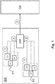
- FIG. 1 schematically shows an exemplary electronic component BE.
- the component BE is designed as an integrated circuit, for example as an application-specific, integrated circuit or ASIC. Alternatively, however, the electronic component BE can also be designed as a so-called Field Programmable Gate Array or FPGA.
- the electronic component BE can be, for example, a system component or part of a system component in an overall system GS, which functions as a superordinate level and is designed, for example, as an embedded system GS.
- electronic component BE has - among others for the sake of simplicity in FIG. 1 not shown units - at two exemplary position P1, P2 a plurality of sensors T1, U1, LZ1, T2, U2, LZ2, which are mounted for example in the semiconductor material of the electronic component BE or the integrated circuit. From the sensors T1, U1, LZ1, T2, U2, LZ2 current values of system parameters such as temperature and voltage and a signal propagation time at the respective position P1, P2 determined. That is to say that first sensors T1, U1, LZ1 determine, for example at a first position P1 of the electronic component BE, current temperature values from a sensor T1, current values from a sensor U1 and current values for the signal propagation time from sensor LZ1.
- the second sensors T2, U2, LZ2 likewise have a sensor T2 for determining current temperature values, a sensor U2 for determining current voltage values and a sensor LZ2, with which current values of the signal propagation time at the second position P2 can be determined.
- the sensors T1, U1, LZ1, T2, U2, LZ2 can be, for example, at least part of an existing infrastructure for a dynamic voltage adjustment for power dissipation minimization or a so-called dynamic voltage scaling (DVS).
- the electronic component BE has a central monitoring unit UW, by which the system according to the invention for a predictive maintenance of the electronic component BE is formed together with the sensors T1, U1, LZ1, T2, U2, LZ2 mounted in the electronic component BE.
- the central monitoring unit UW can be realized as an independent unit or as an independent module in the electronic component BE.
- the central monitoring unit UW can be transformed into a - in FIG. 1 not shown - system unit of the electronic component BE such as a CPU, a processor, etc. be integrated and run by this in the overall system GS as a functional unit.
- the central monitoring unit UW is set up to carry out the method according to the invention for predictive maintenance.
- a first method step 1 the sensors T1, U1, LZ1, T2, U2, LZ2 during the operation of the electronic component BE or of the overall system GS determined at the respective position P1, P2, the current values of the system parameters, in particular of temperature and voltage, and current values of a signal delay.
- the current values of the system parameters and the signal propagation time of the respective position P1, P2 are queried by the central monitoring unit UW.
- a query of the current values of the system parameters and the signal propagation time of the various positions P1, P2 by the central monitoring unit UW can be carried out, for example, continuously during the operation of the electronic component BE.
- the actual values of the system parameters and the signal propagation time determined by the sensors T1, U1, LZ1, T2, U2, LZ2 at the respective positions P1, P2 can also be interrogated during predefined self-test phases, wherein the self-test phases are periodically repeated or run through.
- the central monitoring unit UW uses the actual values of the system parameters determined at the respective position P1, P2, in particular based on the current temperature and voltage values, to set a valid limit value for the signal propagation time at the respective position P1, P2 determined.
- the determination of the respectively determined, valid limit value for the respective signal propagation time at the respective position P1, P2 is carried out in such a way that a respectively critical value for the signal propagation time at the respective position P1, P2 is not exceeded by the respectively determined, valid limit value.
- the respective valid limit value is a specifiable tolerance or guard interval below the respective critical value for the signal propagation time at the respective position P1, P2, wherein upon reaching the critical value for the signal propagation time at a position P1, P2 of the electronic component BE, the electronic Component BE should be replaced, for example due to occurring error conditions or must.
- a first valid limit value for the signal propagation time at the first position P1 is determined by the central monitoring unit UW in the second method step 2. Furthermore, the central monitoring unit UW determines, for the second position P2, on the basis of the second, respectively valid limit value for the signal propagation time at the second position P2, by the second sensors T2, U2.
- the respective valid limit value for the signal propagation time at the respective position P1, P2 is compared by the central monitoring unit UW with the currently determined value of the signal propagation time at the respective position P1, P2.
- the signal propagation time at different positions P1, P2 in the electronic component can slow down even under constant conditions (eg temperature, voltage, load, etc.).
- central monitoring unit UW can detect a significant deceleration of the signal propagation time at the respective position P1, P2 of the electronic component BE. This means that in the FIG.
- electronic component BE is compared by the central monitoring unit, for example, the first valid limit with current, determined values of the signal propagation time, which were determined by the sensor LZ1 at the first position P1.
- the second respectively valid limit value is then compared, for example, with actual, determined values of the signal propagation time which were determined by the sensor LZ2 at the second position P2.
- Step 3 of the central monitoring unit UW sent a message to the higher levels - eg to the overall system GS.
- the message can be sent from the central monitoring unit UW to a central control unit, from which, for example, the entire system GS or several systems are monitored. Due to the message can be reacted to the higher system level GS in a suitable manner - eg by alarms, by triggering appropriate measures, etc. It can, for example, demand-oriented replacement of the electronic component BE or the corresponding system component made or a maintenance of the overall system GS be prompted ,
- FIG. 2 again schematically shows the exemplary electronic component BE, which has the system for predictive maintenance.
- sensors T1, U1, LZ1, T2, U2, LZ2, T3, U3, LZ3 are mounted in the electronic component BE or in the semiconductor material of the electronic component BE, for example at several positions - eg at three positions P1, P2, P3 which current values of the system parameters (eg temperature, voltage) and the signal propagation time at the respective position P1, P2, P3 are determined.
- the system parameters eg temperature, voltage
- a first monitoring element UE1 includes, for example, first sensors T1, U1, LZ1 for determining the current values of the system parameters or of temperature and voltage as well as the signal propagation time at the first position P1.
- Second sensors T2, U2, LZ2 of the second position P2 are combined, for example, in a second monitoring element UE2, and a third monitoring element UE3 comprises, for example, third sensors T3, U3, LZ3 at a third position P3.
- the current values of the system parameters and the signal propagation time at the respective position P1, P2, P3 are again determined during operation in the first method step 1 by the respective sensors T1, U1, LZ1, T2, U2, LZ2, T3, U3, LZ3. Then, the currently determined values of the system parameters and the signal propagation time at the respective position P1, P2, P3 are bundled by the respective monitoring element UE1, UE2, UE3 and can be position-specifically from the respective monitoring element UE1, UE2, UE3 either continuously or while being specifiable by the central monitoring unit UW , Periodic self-test phases of the electronic component BE are queried.
- a valid limit value for the signal propagation time at the respective position P1, P2, P3 is determined by the central monitoring unit UW on the basis of the currently determined values of the system parameters for the respective position P1, P2, P3.
- the respectively valid limit value for the signal propagation time at the respective position P1, P2, P3 is then compared with actual values of the signal propagation time determined for the respective position P1, P2, P3. If at least one of the respectively valid limit values for the signal propagation time at the respective position P1, P2, P3 is exceeded by the corresponding currently determined value of the signal propagation time for the respective position P1, P2, P3, in the third method step 3 a message is sent to the higher level - eg the entire system GS - sent. It can then be initiated again appropriate measures and reactions.
- the second method step 2 of the method according to the invention can be at least partially shifted into the monitoring elements UE1, UE2, UE3. This means that the values of the system parameters and the signal propagation time determined by the respective sensors T1, U1, LZ1, T2, U2, LZ2, T3, U3, LZ3 are already locally evaluated in the respective monitoring element UE1, UE2, UE3.
- this part of the second method step 2 is also performed by the further monitoring element UE2, UE3 for the respective, further positions P2, P3.
- the monitoring elements UE1, UE2, UE3 can then be interrogated by the central monitoring unit UW, for example, and forward the respective comparison result (for example "limit value exceeded", "limit value not exceeded") to the central monitoring unit UW. If the central monitoring unit determines that a response from at least one monitoring element UE1, UE2, UE3 is to "limit value exceeded", the central monitoring unit UW can in the third method step 3 send a message to the higher level
Landscapes
- Engineering & Computer Science (AREA)
- Physics & Mathematics (AREA)
- General Physics & Mathematics (AREA)
- General Engineering & Computer Science (AREA)
- Computer Hardware Design (AREA)
- Microelectronics & Electronic Packaging (AREA)
- Environmental & Geological Engineering (AREA)
- Theoretical Computer Science (AREA)
- Quality & Reliability (AREA)
- Tests Of Electronic Circuits (AREA)
- Testing Of Individual Semiconductor Devices (AREA)
- Debugging And Monitoring (AREA)
Priority Applications (5)
| Application Number | Priority Date | Filing Date | Title |
|---|---|---|---|
| EP17182034.3A EP3432014A1 (fr) | 2017-07-19 | 2017-07-19 | Procédé et système d'entretien préventif des circuits intégrés |
| CN201880047799.6A CN110892277B (zh) | 2017-07-19 | 2018-07-18 | 用于集成电路的预测性维护的方法和系统 |
| PCT/EP2018/069530 WO2019016278A1 (fr) | 2017-07-19 | 2018-07-18 | Procédé et système de maintenance prédictive de circuits intégrés |
| EP18746644.6A EP3610276B1 (fr) | 2017-07-19 | 2018-07-18 | Procédé et système d'entretien préventif des circuits intégrés |
| US16/632,083 US11525858B2 (en) | 2017-07-19 | 2018-07-18 | Method and system for predictive maintenance of integrated circuits |
Applications Claiming Priority (1)
| Application Number | Priority Date | Filing Date | Title |
|---|---|---|---|
| EP17182034.3A EP3432014A1 (fr) | 2017-07-19 | 2017-07-19 | Procédé et système d'entretien préventif des circuits intégrés |
Publications (1)
| Publication Number | Publication Date |
|---|---|
| EP3432014A1 true EP3432014A1 (fr) | 2019-01-23 |
Family
ID=59409167
Family Applications (2)
| Application Number | Title | Priority Date | Filing Date |
|---|---|---|---|
| EP17182034.3A Withdrawn EP3432014A1 (fr) | 2017-07-19 | 2017-07-19 | Procédé et système d'entretien préventif des circuits intégrés |
| EP18746644.6A Active EP3610276B1 (fr) | 2017-07-19 | 2018-07-18 | Procédé et système d'entretien préventif des circuits intégrés |
Family Applications After (1)
| Application Number | Title | Priority Date | Filing Date |
|---|---|---|---|
| EP18746644.6A Active EP3610276B1 (fr) | 2017-07-19 | 2018-07-18 | Procédé et système d'entretien préventif des circuits intégrés |
Country Status (4)
| Country | Link |
|---|---|
| US (1) | US11525858B2 (fr) |
| EP (2) | EP3432014A1 (fr) |
| CN (1) | CN110892277B (fr) |
| WO (1) | WO2019016278A1 (fr) |
Families Citing this family (3)
| Publication number | Priority date | Publication date | Assignee | Title |
|---|---|---|---|---|
| DE102019104246A1 (de) * | 2019-02-20 | 2020-08-20 | Bayerische Motoren Werke Aktiengesellschaft | System und Verfahren zur Überwachung von Halbleiter-Bauteilen eines Fahrzeugs |
| DE102019121903A1 (de) * | 2019-08-14 | 2021-02-18 | Seg Automotive Germany Gmbh | Verfahren zum Herstellen einer Baugruppe mit mehreren Halbleiterbauteilen, Baugruppe und Verwendung einer Baugruppe |
| DE102023127066A1 (de) * | 2023-10-05 | 2025-04-10 | HELLA GmbH & Co. KGaA | Strompfaddiagnose mithilfe einer elektronischen Sicherung |
Citations (4)
| Publication number | Priority date | Publication date | Assignee | Title |
|---|---|---|---|---|
| US20110128055A1 (en) * | 2008-05-29 | 2011-06-02 | Nxp B.V. | Dll for period jitter measurement |
| US20130013247A1 (en) * | 2010-03-15 | 2013-01-10 | Kyushu Institute Of Technology | Semiconductor device, detection method and program |
| US20130080090A1 (en) * | 2010-07-30 | 2013-03-28 | Empire Technology Development Llc | Aging-based usage metering of components |
| US20130093488A1 (en) * | 2011-10-14 | 2013-04-18 | Ravi Karapatti Ramaswami | Test circuit and methods for speed characterization |
Family Cites Families (8)
| Publication number | Priority date | Publication date | Assignee | Title |
|---|---|---|---|---|
| US7248102B2 (en) | 2005-01-20 | 2007-07-24 | Infineon Technologies Ag | Internal reference voltage generation for integrated circuit testing |
| US7797596B2 (en) | 2007-09-26 | 2010-09-14 | Oracle America, Inc. | Method for monitoring and adjusting circuit performance |
| AT506092B1 (de) | 2008-08-13 | 2009-06-15 | Siemens Ag Oesterreich | Elektrische anlage |
| CN101706551B (zh) | 2009-10-30 | 2012-01-04 | 西安电子科技大学 | 预报集成电路负偏压不稳定性失效的测试电路 |
| CN101762781B (zh) | 2010-01-08 | 2012-05-09 | 西安西电科大射频集成电路有限责任公司 | 预报集成电路静电放电失效的测试电路及预测方法 |
| DE102010045278A1 (de) | 2010-09-14 | 2012-03-15 | Phoenix Contact Gmbh & Co. Kg | Vorrichtung zur Betriebsparameter-Überwachung integrierter Schaltkreise und integrierter Schaltkreis mit Betriebsparameter-Überwachung |
| US9587992B1 (en) * | 2013-03-13 | 2017-03-07 | Inphi Corporation | Voltage and temperature sensor for a serializer/deserializer communication application |
| US9823301B2 (en) * | 2014-02-07 | 2017-11-21 | Commissariat à l'énergie atomique et aux énergies alternatives | Method for characterizing the operation of a digital electronic circuit and digital electronic circuit |
-
2017
- 2017-07-19 EP EP17182034.3A patent/EP3432014A1/fr not_active Withdrawn
-
2018
- 2018-07-18 EP EP18746644.6A patent/EP3610276B1/fr active Active
- 2018-07-18 WO PCT/EP2018/069530 patent/WO2019016278A1/fr not_active Ceased
- 2018-07-18 CN CN201880047799.6A patent/CN110892277B/zh active Active
- 2018-07-18 US US16/632,083 patent/US11525858B2/en active Active
Patent Citations (4)
| Publication number | Priority date | Publication date | Assignee | Title |
|---|---|---|---|---|
| US20110128055A1 (en) * | 2008-05-29 | 2011-06-02 | Nxp B.V. | Dll for period jitter measurement |
| US20130013247A1 (en) * | 2010-03-15 | 2013-01-10 | Kyushu Institute Of Technology | Semiconductor device, detection method and program |
| US20130080090A1 (en) * | 2010-07-30 | 2013-03-28 | Empire Technology Development Llc | Aging-based usage metering of components |
| US20130093488A1 (en) * | 2011-10-14 | 2013-04-18 | Ravi Karapatti Ramaswami | Test circuit and methods for speed characterization |
Non-Patent Citations (1)
| Title |
|---|
| S. MITRA; M. AGARWAL: "Circuit failure prediction to overcome scaled CMOS reliability challenges", 2007 IEEE INTERNATIONAL TEST CONFERENCE, 2007, pages 1 - 3, XP031207047, DOI: doi:10.1109/TEST.2007.4437665 |
Also Published As
| Publication number | Publication date |
|---|---|
| US11525858B2 (en) | 2022-12-13 |
| EP3610276B1 (fr) | 2021-01-06 |
| US20200166568A1 (en) | 2020-05-28 |
| CN110892277B (zh) | 2022-06-03 |
| EP3610276A1 (fr) | 2020-02-19 |
| WO2019016278A1 (fr) | 2019-01-24 |
| CN110892277A (zh) | 2020-03-17 |
Similar Documents
| Publication | Publication Date | Title |
|---|---|---|
| EP2040957B1 (fr) | Procédé et dispositif de contrôle de plausibilité de valeurs de mesure dans l'environnement d'un véhicule à moteur | |
| DE102017107284B4 (de) | Verfahren und steuergerät zum überwachen eines bordnetzes eines fahrzeugs | |
| EP2191344B1 (fr) | Ensemble de circuits intégrés pour systèmes de régulation déterminants pour la sécurité | |
| DE102012023350B4 (de) | Systeme, Schaltungen und ein Verfahren zum Erzeugen einer konfigurierbaren Rückmeldung | |
| EP1092177B1 (fr) | Regulateur ou regulateur de propulseur, propulseur et procede pour reguler un systeme de reglage ou d'entrainement ou un propulseur | |
| EP3779365B1 (fr) | Procédé et système doté d'un capteur | |
| EP3610276B1 (fr) | Procédé et système d'entretien préventif des circuits intégrés | |
| EP3657288A1 (fr) | Surveillance sécurisée de la tension | |
| WO2010142535A1 (fr) | Procédé et dispositif visant à contrôler l'absence d'erreurs dans un système global comprenant plusieurs installations | |
| DE202007014753U1 (de) | Schaltung zum Überwachen, ob die Schaltschwelle eines Schaltgebers innerhalb eines vorgegebenen Toleranzbereichs liegt | |
| EP1594021B1 (fr) | Dispositif de circuit et procédé de test de contacts de commutation d'un circuit numérique de sortie | |
| EP3745596A1 (fr) | Circuit d'entrée numérique permettant de recevoir des signaux d'entrée numérique d'au moins un émetteur de signaux | |
| EP2786162B1 (fr) | Procédé de détection d'une erreur dans des lignes de connexion entre une unité centrale et une multiplicité d'unités électroniques indépendantes l'une de l'autre | |
| EP4063981A1 (fr) | Procédé d'exécution d'un processus de réparation automatique sur au moins une unité fonctionnelle d'une unité de base, et produit programme informatique et système de réparation | |
| DE102004033263B4 (de) | Steuer-und Regeleinheit | |
| EP1807760B1 (fr) | Systeme de traitement de donnees a frequence d'horloge variable | |
| EP3281365B1 (fr) | Dispositif d'extension d'interface pour un dispositif réseau et procédé de fonctionnement d'un dispositif d'extension d'interface | |
| EP1692578B1 (fr) | Unite peripherique d'un systeme de commande redondant | |
| EP1933008B1 (fr) | Système de protection pour une installation et procédé destiné à la surveillance d'un système de protection | |
| DE102015203253A1 (de) | Sicherheitsschaltungseinheit | |
| Fourlas et al. | A framework for fault detection of hybrid systems | |
| EP1674955A1 (fr) | Méthode et dispositif de surveillance du mode de fonctionnement d'un système d'automatisation dans une installation technique | |
| WO2018050491A1 (fr) | Surveillance de fonctions pertinentes pour la sécurité par une unité de calcul non sécurisée | |
| WO2016012496A1 (fr) | Procédé de détermination de la fiabilité du système d'un circuit logique | |
| DE102020212313A1 (de) | Verfahren zur Diagnose eines Betriebszustands von Feldgeräten eines industriellen Systems |
Legal Events
| Date | Code | Title | Description |
|---|---|---|---|
| PUAI | Public reference made under article 153(3) epc to a published international application that has entered the european phase |
Free format text: ORIGINAL CODE: 0009012 |
|
| STAA | Information on the status of an ep patent application or granted ep patent |
Free format text: STATUS: THE APPLICATION HAS BEEN PUBLISHED |
|
| AK | Designated contracting states |
Kind code of ref document: A1 Designated state(s): AL AT BE BG CH CY CZ DE DK EE ES FI FR GB GR HR HU IE IS IT LI LT LU LV MC MK MT NL NO PL PT RO RS SE SI SK SM TR |
|
| AX | Request for extension of the european patent |
Extension state: BA ME |
|
| STAA | Information on the status of an ep patent application or granted ep patent |
Free format text: STATUS: THE APPLICATION IS DEEMED TO BE WITHDRAWN |
|
| 18D | Application deemed to be withdrawn |
Effective date: 20190724 |