EP3432069A1 - Élément d'écran et dispositif d'affichage d'image - Google Patents
Élément d'écran et dispositif d'affichage d'image Download PDFInfo
- Publication number
- EP3432069A1 EP3432069A1 EP17766445.5A EP17766445A EP3432069A1 EP 3432069 A1 EP3432069 A1 EP 3432069A1 EP 17766445 A EP17766445 A EP 17766445A EP 3432069 A1 EP3432069 A1 EP 3432069A1
- Authority
- EP
- European Patent Office
- Prior art keywords
- light
- screen member
- image display
- optical
- local
- Prior art date
- Legal status (The legal status is an assumption and is not a legal conclusion. Google has not performed a legal analysis and makes no representation as to the accuracy of the status listed.)
- Withdrawn
Links
- 230000003287 optical effect Effects 0.000 claims abstract description 105
- 239000004065 semiconductor Substances 0.000 claims description 5
- 230000004907 flux Effects 0.000 description 24
- 238000009826 distribution Methods 0.000 description 23
- 238000000034 method Methods 0.000 description 18
- 230000008859 change Effects 0.000 description 13
- 230000000694 effects Effects 0.000 description 13
- 238000010586 diagram Methods 0.000 description 12
- 230000002093 peripheral effect Effects 0.000 description 12
- 238000009877 rendering Methods 0.000 description 8
- 230000000007 visual effect Effects 0.000 description 7
- 238000001514 detection method Methods 0.000 description 6
- 239000003086 colorant Substances 0.000 description 5
- 230000007423 decrease Effects 0.000 description 5
- 230000006870 function Effects 0.000 description 5
- 239000011521 glass Substances 0.000 description 5
- WYTGDNHDOZPMIW-RCBQFDQVSA-N alstonine Natural products C1=CC2=C3C=CC=CC3=NC2=C2N1C[C@H]1[C@H](C)OC=C(C(=O)OC)[C@H]1C2 WYTGDNHDOZPMIW-RCBQFDQVSA-N 0.000 description 4
- 238000003384 imaging method Methods 0.000 description 4
- 239000004973 liquid crystal related substance Substances 0.000 description 4
- 238000004519 manufacturing process Methods 0.000 description 3
- 206010047571 Visual impairment Diseases 0.000 description 2
- 238000003491 array Methods 0.000 description 2
- 230000015572 biosynthetic process Effects 0.000 description 2
- 230000001678 irradiating effect Effects 0.000 description 2
- 229910052451 lead zirconate titanate Inorganic materials 0.000 description 2
- 239000011347 resin Substances 0.000 description 2
- 229920005989 resin Polymers 0.000 description 2
- 230000008901 benefit Effects 0.000 description 1
- 230000000903 blocking effect Effects 0.000 description 1
- 230000000052 comparative effect Effects 0.000 description 1
- 230000008878 coupling Effects 0.000 description 1
- 238000010168 coupling process Methods 0.000 description 1
- 238000005859 coupling reaction Methods 0.000 description 1
- 238000005520 cutting process Methods 0.000 description 1
- 230000003247 decreasing effect Effects 0.000 description 1
- 238000001312 dry etching Methods 0.000 description 1
- 230000002708 enhancing effect Effects 0.000 description 1
- 230000007613 environmental effect Effects 0.000 description 1
- 238000005530 etching Methods 0.000 description 1
- 230000006872 improvement Effects 0.000 description 1
- 238000001746 injection moulding Methods 0.000 description 1
- 230000002452 interceptive effect Effects 0.000 description 1
- HFGPZNIAWCZYJU-UHFFFAOYSA-N lead zirconate titanate Chemical compound [O-2].[O-2].[O-2].[O-2].[O-2].[Ti+4].[Zr+4].[Pb+2] HFGPZNIAWCZYJU-UHFFFAOYSA-N 0.000 description 1
- 230000007246 mechanism Effects 0.000 description 1
- 230000005499 meniscus Effects 0.000 description 1
- 230000004048 modification Effects 0.000 description 1
- 238000012986 modification Methods 0.000 description 1
- 238000000206 photolithography Methods 0.000 description 1
- 230000008569 process Effects 0.000 description 1
- 230000009467 reduction Effects 0.000 description 1
- 230000004044 response Effects 0.000 description 1
- 238000004544 sputter deposition Methods 0.000 description 1
- 239000000758 substrate Substances 0.000 description 1
- 238000001771 vacuum deposition Methods 0.000 description 1
Images


Classifications
-
- G—PHYSICS
- G02—OPTICS
- G02B—OPTICAL ELEMENTS, SYSTEMS OR APPARATUS
- G02B3/00—Simple or compound lenses
- G02B3/0006—Arrays
- G02B3/0037—Arrays characterized by the distribution or form of lenses
- G02B3/0056—Arrays characterized by the distribution or form of lenses arranged along two different directions in a plane, e.g. honeycomb arrangement of lenses
-
- G—PHYSICS
- G02—OPTICS
- G02B—OPTICAL ELEMENTS, SYSTEMS OR APPARATUS
- G02B26/00—Optical devices or arrangements for the control of light using movable or deformable optical elements
- G02B26/08—Optical devices or arrangements for the control of light using movable or deformable optical elements for controlling the direction of light
- G02B26/0816—Optical devices or arrangements for the control of light using movable or deformable optical elements for controlling the direction of light by means of one or more reflecting elements
- G02B26/0833—Optical devices or arrangements for the control of light using movable or deformable optical elements for controlling the direction of light by means of one or more reflecting elements the reflecting element being a micromechanical device, e.g. a MEMS mirror, DMD
-
- G—PHYSICS
- G02—OPTICS
- G02B—OPTICAL ELEMENTS, SYSTEMS OR APPARATUS
- G02B27/00—Optical systems or apparatus not provided for by any of the groups G02B1/00 - G02B26/00, G02B30/00
- G02B27/01—Head-up displays
- G02B27/0101—Head-up displays characterised by optical features
-
- G—PHYSICS
- G02—OPTICS
- G02B—OPTICAL ELEMENTS, SYSTEMS OR APPARATUS
- G02B3/00—Simple or compound lenses
- G02B3/0006—Arrays
- G02B3/0037—Arrays characterized by the distribution or form of lenses
-
- G—PHYSICS
- G02—OPTICS
- G02B—OPTICAL ELEMENTS, SYSTEMS OR APPARATUS
- G02B3/00—Simple or compound lenses
- G02B3/02—Simple or compound lenses with non-spherical faces
- G02B3/04—Simple or compound lenses with non-spherical faces with continuous faces that are rotationally symmetrical but deviate from a true sphere, e.g. so called "aspheric" lenses
-
- G—PHYSICS
- G02—OPTICS
- G02B—OPTICAL ELEMENTS, SYSTEMS OR APPARATUS
- G02B3/00—Simple or compound lenses
- G02B3/02—Simple or compound lenses with non-spherical faces
- G02B3/06—Simple or compound lenses with non-spherical faces with cylindrical or toric faces
-
- G—PHYSICS
- G03—PHOTOGRAPHY; CINEMATOGRAPHY; ANALOGOUS TECHNIQUES USING WAVES OTHER THAN OPTICAL WAVES; ELECTROGRAPHY; HOLOGRAPHY
- G03B—APPARATUS OR ARRANGEMENTS FOR TAKING PHOTOGRAPHS OR FOR PROJECTING OR VIEWING THEM; APPARATUS OR ARRANGEMENTS EMPLOYING ANALOGOUS TECHNIQUES USING WAVES OTHER THAN OPTICAL WAVES; ACCESSORIES THEREFOR
- G03B21/00—Projectors or projection-type viewers; Accessories therefor
- G03B21/54—Accessories
- G03B21/56—Projection screens
- G03B21/60—Projection screens characterised by the nature of the surface
- G03B21/62—Translucent screens
-
- H—ELECTRICITY
- H04—ELECTRIC COMMUNICATION TECHNIQUE
- H04N—PICTORIAL COMMUNICATION, e.g. TELEVISION
- H04N9/00—Details of colour television systems
- H04N9/12—Picture reproducers
- H04N9/31—Projection devices for colour picture display, e.g. using electronic spatial light modulators [ESLM]
- H04N9/3129—Projection devices for colour picture display, e.g. using electronic spatial light modulators [ESLM] scanning a light beam on the display screen
-
- H—ELECTRICITY
- H04—ELECTRIC COMMUNICATION TECHNIQUE
- H04N—PICTORIAL COMMUNICATION, e.g. TELEVISION
- H04N9/00—Details of colour television systems
- H04N9/12—Picture reproducers
- H04N9/31—Projection devices for colour picture display, e.g. using electronic spatial light modulators [ESLM]
- H04N9/3141—Constructional details thereof
- H04N9/315—Modulator illumination systems
- H04N9/3155—Modulator illumination systems for controlling the light source
-
- H—ELECTRICITY
- H04—ELECTRIC COMMUNICATION TECHNIQUE
- H04N—PICTORIAL COMMUNICATION, e.g. TELEVISION
- H04N9/00—Details of colour television systems
- H04N9/12—Picture reproducers
- H04N9/31—Projection devices for colour picture display, e.g. using electronic spatial light modulators [ESLM]
- H04N9/3179—Video signal processing therefor
- H04N9/3182—Colour adjustment, e.g. white balance, shading or gamut
-
- G—PHYSICS
- G02—OPTICS
- G02B—OPTICAL ELEMENTS, SYSTEMS OR APPARATUS
- G02B27/00—Optical systems or apparatus not provided for by any of the groups G02B1/00 - G02B26/00, G02B30/00
- G02B27/01—Head-up displays
- G02B27/0101—Head-up displays characterised by optical features
- G02B2027/011—Head-up displays characterised by optical features comprising device for correcting geometrical aberrations, distortion
-
- G—PHYSICS
- G02—OPTICS
- G02B—OPTICAL ELEMENTS, SYSTEMS OR APPARATUS
- G02B27/00—Optical systems or apparatus not provided for by any of the groups G02B1/00 - G02B26/00, G02B30/00
- G02B27/01—Head-up displays
- G02B27/0101—Head-up displays characterised by optical features
- G02B2027/0118—Head-up displays characterised by optical features comprising devices for improving the contrast of the display / brillance control visibility
-
- G—PHYSICS
- G02—OPTICS
- G02B—OPTICAL ELEMENTS, SYSTEMS OR APPARATUS
- G02B27/00—Optical systems or apparatus not provided for by any of the groups G02B1/00 - G02B26/00, G02B30/00
- G02B27/01—Head-up displays
- G02B27/0101—Head-up displays characterised by optical features
- G02B2027/0145—Head-up displays characterised by optical features creating an intermediate image
-
- G—PHYSICS
- G02—OPTICS
- G02B—OPTICAL ELEMENTS, SYSTEMS OR APPARATUS
- G02B27/00—Optical systems or apparatus not provided for by any of the groups G02B1/00 - G02B26/00, G02B30/00
- G02B27/01—Head-up displays
-
- G—PHYSICS
- G09—EDUCATION; CRYPTOGRAPHY; DISPLAY; ADVERTISING; SEALS
- G09G—ARRANGEMENTS OR CIRCUITS FOR CONTROL OF INDICATING DEVICES USING STATIC MEANS TO PRESENT VARIABLE INFORMATION
- G09G3/00—Control arrangements or circuits, of interest only in connection with visual indicators other than cathode-ray tubes
- G09G3/02—Control arrangements or circuits, of interest only in connection with visual indicators other than cathode-ray tubes by tracing or scanning a light beam on a screen
Definitions
- the disclosures herein generally relate to a screen member, an image display apparatus, and an object apparatus.
- Patent Document 1 discloses a screen member having a plurality of optical elements (such as lenses and mirrors) provided in an array.
- Patent Document 1 Japanese Patent No. 5310810
- the screen member disclosed Patent Document 1 has scope for improvement in enhancing visibility while securing a visual field.
- a screen member irradiated with image display light includes at least one optical surface configured to reflect or refract light, wherein an absolute value of a local curvature of the optical surface changes in one direction, and becomes a local minimum at at least one position.
- HUD is an abbreviation for a head-up display.
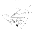
- FIG. 1 schematically illustrates a general arrangement of the HUD apparatus 100 according to the present embodiment.
- a projection method of a head-up display there is a panel method and a laser scanning method.
- an intermediate image is formed by using an imaging device such as a liquid crystal panel, a digital mirror device (DMD) panel, or a vacuum fluorescent display (VFD).
- an imaging device such as a liquid crystal panel, a digital mirror device (DMD) panel, or a vacuum fluorescent display (VFD).
- VFD vacuum fluorescent display
- an intermediate image is formed by scanning a laser beam emitted from a laser beam source by using a two-dimensional scanning device.
- the laser scanning method forms an image by assigning light emission and non-light emission for each pixel, allowing a high-contrast image to be formed.
- the HUD apparatus 100 employs the laser scanning method.
- the above-described panel method may also be used as a projection method.
- the HUD apparatus 100 is installed in a moving object such as a vehicle, an aircraft, a ship, or an industrial robot, and causes navigation information (such as a speed of the moving object, a travelling direction, a distance to a destination, a name of a current location, a presence or a position of an object in front of the moving object, signs such as speed limits, and traffic congestion information) required for the steering of the moving object to be visible on a front windshield 50 (see FIG. 1 ) of the moving object.
- the front windshield 50 also functions as a transmissive reflection member configured to transmit part of incident light and reflects at least part of the rest of the incident light.
- the HUD apparatus 100 includes the front windshield 50.
- the HUD apparatus 100 includes: an optical scanning device 10 including a light source device 11, an optical deflector 15, and a scanning mirror 20; a screen 30; and a concave mirror 40.
- an optical scanning device 10 including a light source device 11, an optical deflector 15, and a scanning mirror 20; a screen 30; and a concave mirror 40.
- a virtual image I can be made visible on the front windshield 50 from a viewpoint position of a viewer A (a driver who is an occupant of the automobile). Namely, the viewer A can visually identify an image (an intermediate image) formed (rendered) on the screen 30 as a virtual image I through the front windshield 50.
- the HUD apparatus 100 is disposed below a dashboard of the automobile, and a distance between the viewpoint position of the viewer A and the front windshield 50 is approximately several tens of centimeters to 1 meter.
- the concave mirror 40 is designed to have given converging power by using an existing optical design simulation software such that the virtual image I is formed at a desired position.
- the converging power of the concave mirror 40 is preferably set such that the virtual image I is formed at a position (a depth position) greater than or equal to 1 m to less than or equal to 10 m (preferably less than or equal to 6 m) away from the viewpoint position of the viewer A.
- the front windshield is not flat, but is slightly curved. Therefore, an image forming position of the virtual image I is determined by both the concave mirror 40 and the curved surface of the front windshield 50.
- the light source device 11 combines laser beams of three colors, red, green, and blue that are modulated in accordance with image data.
- the combined laser beam (in which the laser beams of the three colors are combined) is directed toward a reflective surface of the optical deflector 15.
- the optical deflector 15 is a two-axis microelectromechanical systems (MEMS) scanner manufactured by a semiconductor manufacturing process, and includes a single micro-mirror 150 (see FIG. 5 ) that can independently oscillate around two axes orthogonal to each other.
- MEMS microelectromechanical systems
- Light (pixel display light) emitted from the light source device 11 in accordance with the image data is deflected by the optical deflector 15, reflected by the scanning mirror 20, and irradiated to the screen 30.
- the concave mirror 40 is preferably designed and arranged to correct optical distortion that causes a horizontal line of an intermediate image to become upwardly or downwardly convex due to the shape of the front windshield 50.
- the light that has passed through the screen 30 is reflected by the concave mirror 40 toward the front windshield 50.
- Part of the light incident on the front windshield 50 is transmitted through the front windshield 50 and at least part of the rest of the light is reflected toward the viewpoint position of the viewer A.
- the viewer A can visually identify an enlarged virtual image I of the intermediate image through the front windshield A. Namely, when viewed from the viewer A, the virtual image I is enlargedly displayed through the front windshield 50.
- a combiner may be provided as a transmissive reflection member on the viewpoint position side of the viewer A relative to the front windshield 50. Similarly to a case in which only the front windshield 50 is irradiated with light from the concave mirror 40, a virtual image may be displayed by irradiating the combiner with light from the concave mirror 40.
- FIG. 2 is a block diagram illustrating a hardware configuration of a control system of the HUD apparatus 100.
- the control system of the HUD apparatus 100 includes a field-programmable gate array (FPGA) 600, a central processing unit (CPU) 602, read-only memory (ROM) 604, an interface (I/F) 608, a bus-line 610, a laser diode (LD) driver 6111, and a MEMS controller 615.
- FPGA field-programmable gate array
- CPU central processing unit
- ROM read-only memory
- I/F interface
- bus-line 610 a bus-line 610
- LD laser diode
- MEMS controller 615 MEMS controller
- the FPGA 600 drives LDs, which will be described later, by means of the LD driver 6111, and drives the optical deflector 15 by means of the MEMS controller 615.
- the CPU 602 controls functions of the HUD apparatus 100.
- the ROM 604 stores image processing programs executed by the CPU 602 to control the functions of the HUD apparatus 100.
- Random access memory (RAM) 606 is used as a work area of the CPU 602.
- the I/F 608 is an interface for communicating with an external controller and the like. For example, the I/F 608 is coupled to a Controller Area Network (CAN) of the automobile.
- CAN Controller Area Network
- FIG. 3 is a block diagram illustrating functions of the HUD apparatus.
- the HUD apparatus includes a vehicle information input unit 800, an external information input unit 802, an image data generating unit 804, and an image rendering unit 806.
- Information relating to a vehicle information such as a speed, a travel distance, a distance to an object, and outside brightness
- External information information such as navigation information from the global positioning system (GPS)
- GPS global positioning system
- the image data generating unit 804 generates image data of an image to be rendered, based on information input in the vehicle information input unit 800 and in the external information input unit 802, and sends the generated image data to the FPGA 600.
- the image rendering unit 806 includes a control unit 8060.
- the control unit 8060 sends a control signal for starting or finishing rendering an image to FPGA 600.
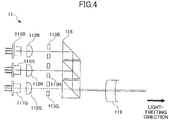
- FIG. 4 illustrates a configuration of the light source device 11.
- the light source device 11 includes a plurality of light emitting elements 111R, 111B, and 111G each having one or more light emitting points.
- the light emitting elements are laser diodes (LDs) and emit light flux having different wavelengths ⁇ R, ⁇ G, and ⁇ B, respectively.
- ⁇ R is 640 nm
- ⁇ G is 530 nm
- ⁇ B is 445 nm.
- the light fluxes having the wavelengths ⁇ R, ⁇ G, and ⁇ B emitted from the LDs 111R, 111G, and 111B are coupled to a subsequent optical system by corresponding coupling lenses 112R, 112G, and 112B, respectively.
- the light fluxes coupled to the optical system are shaped by corresponding aperture members 113R, 113G, and 113B.
- a shape of each of the aperture members may be set to any of various shapes, including a circular shape, an ellipse shape, a rectangular shape, and a square shape depending on, for example, the divergence angle of the light flux.
- the combining element 115 is a platelike or a prismatic dichroic mirror, and reflects or transmits a light flux therethrough in accordance with the wavelength and combines the light fluxes into a single optical path.
- the combined light flux is guided to the reflective surface of the optical deflector 15 by a lens 119.
- the lens 119 is a meniscus lens whose concave surface faces the optical deflector 15.
- FIG. 5 illustrates a configuration of the optical deflector 15.
- the optical deflector 15 is a two-axis MEMS scanner manufactured by a semiconductor manufacturing process, and includes a mirror 150 having a reflective surface and also includes a pair of serpentine units 152, as illustrated in FIG. 5 .
- the serpentine units 152 include a plurality of beams arranged in the X-axis direction, and neighboring two beams are connected to each other through a turning portion so as to meander. Neighboring two beams of the serpentine units 152 are referred to as a beam A (152a) and a beam B (152b), and are supported by a frame 154.
- a plurality of piezoelectric members 156 (for example, lead zirconate titanate (PZT)) is provided for the respective beams.
- PZT lead zirconate titanate
- two neighboring beams are deflected in different directions.
- the mirror 150 is caused to rotate at a large angle around the ⁇ -axis (in the vertical direction).
- optical scanning around the ⁇ -axis in the vertical direction can be performed at low voltage.
- resonant optical scanning around the ⁇ axis in the horizontal direction is performed using, for example, a torsion bar that is connected to the mirror 150.
- an imaging position of a virtual image formed by the HUD apparatus 100 may be set to any position in a predetermined display region where the virtual image can be formed.
- the display region is determined by design at the design phase of the HUD apparatus.
- the panel is required to be entirely irradiated with light. Therefore, because of the nature of the liquid crystal panel or the DMD panel, it is difficult to completely set the luminance to zero even with an image signal for the non-display state being sent. As a result, there may be a case in which black floating is seen. In the laser scanning method, it is possible to eliminate such black floating.
- the FPGA 600 controls the light-emission intensity, the timing of light emission, and the light waveform of each of the light emitting elements of the light source device 11, and the LD driver 6111 drives each of the light emitting elements to emit light.
- Light emitted from each of the light emitting elements and combined into a single optical path is two-dimensionally deflected by the optical deflector 15 around the X-axis and the Y-axis as illustrated in FIG. 6 , and the screen 30 is irradiated with the deflected light that has passed through the scanning mirror 20 (see FIG. 1 ).
- the deflected light serves as scanning light.
- the screen 30 is two-dimensionally scanned by the scanning light. In FIG. 6 , the scanning mirror 20 is not illustrated.
- the screen 30 includes a scanning light detection unit 60 in a peripheral region of an image rendering region (also referred to as an "effective scanning region").
- the scanning light detection unit 60 is disposed to detect an operation of the optical deflector 15. Further, the scanning light detection unit 60 is used to maintain image quality at a certain level by detecting scanning timing (a scanning position of a beam) in response to light emitted onto a signal region and by controlling characteristic changes of the optical deflector 15 associated with an environmental change or a change over time.
- an optical deflector such as a photodiode or a phototransistor can be used as the scanning light detection unit 60.
- An output signal from the scanning light detection unit 60 is sent to the FPGA 600.
- the FPGA 600 generates modulated signals (pulse signals) for the respective colors based on an output signal and image data from the detection unit 60, and sends the generated signals to the LD driver 6111.
- the LD driver 6111 applies driving currents corresponding to the modulated signals for respective colors to the light emitting elements corresponding to the respective colors. Accordingly, a color image (an intermediate image) in accordance with the image data is rendered on the screen 30.
- the screen 30 provided in a scanning range is scanned by scanning light in an oscillating manner (two-way scan) in a main scanning direction at a high frequency of about 20,000 to 40,000 hertz (Hz), and is scanned by scanning light (one-way scan) in a subscanning direction at a low frequency of about a few tens of Hz. Namely, raster scanning is performed. At this time, light emission of each of the light emitting elements is controlled in accordance with the scanning position (the position of the scanning light). Accordingly, an image can be rendered and a virtual image can be displayed per pixel. In FIG. 7 , the number of scanning lines is less than the actual number of scanning lines for convenience of explanation.
- the term "scanning range” refers to the entire range that can be scanned by the optical deflector 15.
- the image rendering region is illustrated as a rectangle shape, but may be distorted to a trapezoid shape or a circular sector shape. In particular, when the screen 30 is directly irradiated with light deflected by the optical deflector 15, it is inevitable that the image rendering region is distorted.
- an in-vehicle HUD is assumed to be used in an environment where brightness changes depending on the surrounding environment (for example, the entrance or exit of a tunnel and a road condition), the time of a day, the weather, and the like.
- a wide dynamic range is required for luminance of an image displayed.
- a display area on the screen greatly changes. This is because, for example, display and non-display of an image are switched as necessary.
- the screen 30 In the HUD apparatus 100 according to the present embodiment, a structure of the screen 30 is devised. In the following, the screen 30 will be described in detail.
- the screen 30 has a microlens array structure having microlenses 300, which are micro-convex lenses, arranged without a gap in the image rendering region on the surface of the incident side.
- the microlenses 300 each cause a laser beam, which is emitted from the light source device 11 and passes through the optical deflector 15 and the scanning mirror 20, to diverge at a desired divergence angle (see FIG. 9A ).
- an X-axis is a horizontal direction
- a Z-axis is an optical axis direction of each of the microlenses.
- the optical axis of each of the microlenses refers to a straight line passing through the optical center and the focal point of each of the microlenses.
- pixel display light refers to light of "image display light” for each pixel.
- a plurality of pixel display light beams forming the image display light is in one-to-one correspondence with the plurality of microlenses 300. Namely, each of the pixel display light beams is approximately entirely incident within an effective diameter range of the corresponding microlens 300.
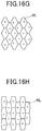
- the microlenses 300 each have a six-sided shape in planar view with a width of approximately a few hundred micrometers, for example.
- the six-sided shape allows the microlenses 300 to be most closely arranged.
- the shape of the microlenses 300 is not limited to the six-sided shape.
- the microlenses 300 may have a rectangular shape or a triangle shape.
- the screen 30 includes an optical plate 301 in which a microlens array (MLA) (microlens array structure) having the plurality of two-dimensionally arranged microlenses is formed on the surface of the incident side (the surface on the +Z side and parallel to a XY-plane) (see FIG. 9A ).
- MLA microlens array
- the screen 30 is made of a resin or glass, for example.
- the plurality of microlenses 300 is two-dimensionally arranged along the XY-plane.
- the light flux diverges and becomes divergent light 303.
- the structure of the microlenses 300 allows the incident light flux to diverge at a desired divergence angle 304.
- an arrangement period 305 of microlens array lenses is designed to be larger than a diameter 306 of the incident light flux. This prevents interference between the lenses and also prevents speckles from appearing.
- FIG. 9B illustrates an optical path of divergent light when light flux 311 has a diameter twice as large as an arrangement period 312 of the microlens array.
- the light flux 311 is concurrently incident on two lenses 313 and 314 and two divergent light beams 315 and 316 are formed.
- the two divergent light beams are concurrently present in a region 317, the two divergent light beams interfere with each other.
- speckles are observed.
- the arrangement period 305 of the microlens array is designed to be larger than the diameter 306 of the light flux such that speckles can be reduced.
- the arrangement period 305 of the lenses is designed to be 110 pm, 150 pm, or 200 pm, for example.
- FIG. 9 illustrates convex lenses, concave lenses exhibit a similar effect.
- FIG. 10 illustrates superimposed cross-sections including optical axes of two microlens arrays each, from a microlens array of spherical lenses and from a microlens array of aspherical lenses.
- a continuous line indicates a spherical surface (a curvature Cs)
- a dashed line indicates an aspherical surface (local curvatures (CX and CY)).
- CX and CY local curvatures
- CX and CY local curvatures
- CX and CY local curvatures in the X-direction and in the Y-direction, respectively.
- CX and CY represent local curvatures in the X-direction and in the Y-direction, respectively.
- "C" represents at least one of CX and CY.
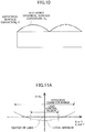
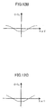
- FIG. 11A and FIG. 11B each illustrate curvature distribution of aspherical lenses AL1 and AL2 with respect to the curvature Cs of a spherical lens.
- the aspherical lenses AL1 and AL2 are specific examples of an aspherical lens AL used as each of the microlenses 300 in the microlens array (MLA) according to the present embodiment.
- Geometrical centers of the lenses illustrated in FIG. 11A and FIG. 11B coincide with each other and the geometrical centers are each regarded as the origin of the X-axis and the Y-axis.
- the optical center and the geometrical center coincide with each other in planar view (when viewed in the Z-axis direction).
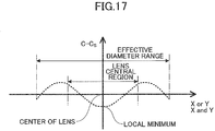
- At least one of absolute values of local curvatures CX and CY becomes a local minimum in a region (also referred to as a "lens central region") that includes a point of intersection (also referred to as a "a center of the lens surface” or a “center of the lens”) of a lens surface and an optical axis.
- the size of the lens central region is determined by the optical design (for example, the size and the position of the observer's eye box) of the HUD apparatus 100.
- the density of divergent light flux increases. Namely, by designing the aspherical lens AL such that the absolute value of a local curvature of the lens surface becomes a local minimum near the center of the lens, the density of divergent light flux increases and luminance improves.
- a curve (a dashed line) indicating curvature distribution on the lens surface is a downward convex curve having a local minimum (see FIG. 11A ).
- a curve (a dashed line) indicating curvature distribution on the lens surface is a curve having a local minimum and inflection points on both sides of the local minimum (see FIG. 11B ).
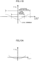
- Such an effect can be obtained not only when absolute values of local curvatures of the lens surface become local minima in both the X-direction and the Y-direction, but also when an absolute value becomes a local minimum in one of the X-direction and the Y-direction and does not become a local minimum in the other direction (see dashed lines in FIGS. 12A through 12D ).
- the absolute values of the local curvatures CX and CY become the local minima, points at which the absolute values become the local minima coincide. Therefore, in terms of symmetry with respect to the X-axis and the Y-axis, it is preferable to have the local minima at the center of the lens.
- the absolute values of the curvatures CX and CY may take the local minima at a point shifted from the center of the lens in at least one of the X-direction and the Y-direction.
- an absolute value of a local curvature of the lens surface may become a local minimum or does not necessarily become a local minimum.
- absolute values of local curvatures of the lens surface become local minima in both the X-direction and the Y-direction (when points at which the absolute values become the local minima coincide)
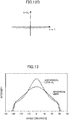
- a dashed line schematically indicates a divergence profile of the spherical lens and a continuous line schematically indicates a divergence profile of the aspherical lens AL according to the present embodiment.
- Each of the lenses is designed to have a reference curvature such that light flux diverges within a region of approximately ⁇ 30 degrees.
- the aspherical lens AL is designed such that an absolute value of a local curvature becomes a local minimum at the center of the lens. Accordingly, the density of divergence light flux becomes high, and luminance can be significantly improved.
- the curvature distribution of the lens is set such that an absolute value of a local curvature becomes a local minimum in a specific region corresponding to a desired region within a viewing range. Accordingly, while light flux incident on the lens can reach the viewing range as in the conventional manner, a divergence angle of light flux incident on a region where the absolute values become the local minima becomes smaller than that of the peripheral region, and thus the light beam density increases.
- the above-described effect of improving luminance can be exhibited when an absolute value of a local curvature of the lens surface becomes a local minimum in at least one of the X-direction and the Y-direction.
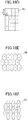
- FIGS. 14A through 14C illustrate angular distribution of divergence intensities after light passes through a six-sided microlens (a spherical lens) in planar view according to a comparative example.
- FIGS. 15A through 15C illustrate angular distribution of divergence intensities after light passes through the six-sided microlens (the aspherical lens AL) in planar view according to the present embodiment.
- both lenses indicate that changes in divergence intensities are moderate.
- peaks of the intensities in FIGS. 15A through 15C are significantly higher than those in FIGS. 14A through 14C .
- an absolute value of a local curvature can be set to a local minimum in the desired region. Therefore, it is possible to exhibit the above-described effect by setting the absolute value of the local curvature to the local minimum.
- an outer diameter of each of the lenses can be selected in such a manner that reduces interference by adjusting the aspect ratio of each of the lenses in accordance with the beam diameter or that controls vertical and horizontal divergence angles.
- an absolute value of a local curvature can be set to a local minimum in the lens central region.
- in-phase interference fringes or moire fringes are not likely to occur because the optical centers of the aspherical lens AL are non-periodically arranged.
- the aspherical lenses AL may have shapes different from each other.
- the microlens array (MLA) is technically achievable by using a known method.
- the microlens array (MLA) is made by injection molding using a mold.
- the microlens array (MLA) can be made by using a cutting method that forms aspherical lens shapes on a mold, or can be made by controlling selectivity such as designing a mask and adjusting a gas flow rate ratio when creating a curved surface of a mold by photolithography or dry etching.
- the screen 30 of the above-described embodiment is a screen member irradiated with image display light, and includes a plurality of microlenses 300 (optical elements) each having a lens surface (an optical surface that reflects light) on one side (an incident side).
- An absolute value of a local curvature of the lens surface changes in at least one of an X-direction and a Y-direction (two directions) in such a manner that becomes a local minimum at at least one position.
- the above two directions are perpendicular to each other on a plane (XY-plane) that is perpendicular to an optical axis of each of the microlenses 300.
- the absolute value of the local curvature of the lens surface becomes the local minimum, and thus luminance of the light can improve. Further, in the predetermined region that has the local minimum, the absolute value of the local curvature gradually increases from a position at which the absolute value becomes the local minimum toward the outer edge of the lens surface. Accordingly, the degree of light divergence can be controlled, and also the visual field can be prevented from being narrowed.
- a divergence profile changes by forming distribution of local curvatures on the lens surface.
- an absolute value of a local curvature is set smaller in a specific region of the lens surface corresponding to a desired region in a viewing range.
- the curvature distribution is set such that the absolute value becomes a local minimum in the specific region. Accordingly, light flux incident on each of the microlenses 300 can reach the viewing range as in the conventional manner. Also, a divergence angle of light flux incident on a region where an absolute value of a local curvature becomes a local minimum becomes smaller than that of the peripheral region, and thus the light beam density increases and luminance improves. As a result, visibility can be improved.
- Patent Document 1 discloses a method for setting "a curvature corresponding to a main viewing region" to be smaller than "curvatures corresponding to sub viewing regions” such that sub-viewing ranges are provided while securing luminance of a main viewing range.
- a required viewing angle (visual field) becomes unable to be obtained.
- the absolute value of the local curvature of the lens surface becomes the local minimum preferably in a region that includes a point of intersection of the lens surface and the optical axis of each of the microlenses 300.
- luminance of pixel display light can significantly improve by illuminating the lens surface with the pixel display light such that the light is incident on the region that includes the above-described point of intersection.
- the absolute value of the local curvature of the lens surface preferably changes such that the absolute value becomes a local minimum in each of the X-direction and the Y-direction.
- the absolute value of the local curvature of the lens surface preferably changes such that the absolute value becomes the local minimum in each of the X-direction and the Y-direction at the point of intersection described above.
- luminance can be improved in the region that includes the above-described point of intersection.
- an average absolute value of local curvatures of the lens surface in the X-direction may be different from that in the Y-direction.
- divergence angles in the X-direction and the Y-direction can be individually controlled.
- light utilization efficiency can be improved.
- a divergence angle in the X-direction can be made larger in order to increase a viewing angle in the horizontal direction where a wide viewing angle is required.
- a divergence angle in the Y-direction can be made smaller in order to decrease a viewing angle in the vertical direction where a wide viewing angle is not required.
- light utilization efficiency can be improved, compared to when divergence angles in the X-direction and the Y-direction are made larger or made smaller at the same rate.
- the absolute value of the local curvature of the lens surface preferably changes so as to be differentiable at a given position in at least one of the directions.
- the number of local minima for the absolute value of the local curvature of the lens surface in at least one of the directions (in which the absolute value becomes the local minimum) may be 1, and the differentiated value at a given position other than the position at which the absolute value becomes the local minimum may be a value other than 0.
- the local minimum for the absolute value of the local curvature of the lens surface can monotonically decrease on one side and the local minimum can monotonically increase on the other side. Accordingly, a preferable divergence profile can be obtained (see FIG. 13 ).
- the absolute value of the local curvature of the lens surface preferably changes in a curved shape in at least one of the directions (in which the absolute value becomes the local minimum).
- the absolute value of the local curvature of the lens surface can smoothly change in at least one of the directions.
- luminance can smoothly change in at least one of the directions.
- discomfort with visibility can be suppressed entirely on the lens surface in at least one of the directions.
- the absolute value of the local curvature preferably changes so as to be approximately line symmetrical about the optical axis of each of the microlenses 300 in at least one of the directions (in which the absolute value becomes the local minimum).
- a divergence profile can be axially symmetrical about the optical axis of each of the microlenses 300 in at least one of the above-described directions.
- divergence characteristics and luminance characteristics on one side of the optical axis can become the same as those on the other side of the optical axis in at least one of the above-described directions.
- the absolute value of the local curvature does not necessarily change so as to be approximately line symmetrical about the optical axis of each of the microlenses 300 in at least one of the directions (in which the absolute value becomes the local minimum). Even in this case, the above-described effect can be provided by causing the absolute value of the local curvature to have a local minimum.
- optical center of each of the microlenses 300 can be randomly (irregularly) shifted from the geometrical center in planar view.
- the HUD apparatus 100 (an image display apparatus) according to the present embodiment includes the light source device 11 (a light source unit) configured to emit light (pixel display light) modulated in accordance with image data, the optical deflector 15 (an image display light generating element) configured to generate image display light based on the light (the pixel display light) emitted from the light source device 11, and the screen 30 irradiated with the image display light.
- the light source device 11 a light source unit
- the optical deflector 15 an image display light generating element
- the HUD apparatus with improved visibility can be provided.
- pixel display light (light of image display light for each pixel) is preferably incident on a region that includes a point of intersection of the lens surface and the optical axis of each of the microlenses 300 on the screen 30.
- the HUD apparatus with significantly improved visibility can be provided.
- the light source device 11 preferably includes a semiconductor laser.
- the HUD apparatus 100 includes the concave mirror 40 (a light projecting unit) configured to project light (image display light), which has passed through the screen 30, onto the front windshield 50 (the transmissive reflection member).
- the concave mirror 40 a light projecting unit
- the front windshield 50 the transmissive reflection member
- a movable apparatus including the HUD apparatus 100 and a moving object in which the HUD apparatus 100 is installed, display images with high visibility can be provided to an occupant of the moving object.
- the screen 30 of the present embodiment is a screen member irradiated with image display light and includes a plurality of microlenses 300 (optical elements) each having a lens surface (an optical surface that reflects light) on one side (an incident side) .
- the absolute value of the local curvature of the lens surface gradually increases from a predetermined position (such as a position at which an absolute value becomes a local minimum) within the region toward the outer edge of the lens surface in at least one of an X-direction and a Y-direction (two directions).
- the two directions are perpendicular to each other on a plane (XY-plane) that is perpendicular to an optical axis of each of the microlenses 300.
- the absolute value of the local curvature of the lens surface becomes the local minimum, and also improve luminance of the light. Further, in the predetermined region that has the local minimum, the absolute value of the local curvature increases from the position at which the absolute value becomes the local minimum toward the outer edge of the lens surface. Accordingly, the degree of light divergence can be controlled. Also, the visual field can be prevented from being narrowed.
- the curvature of the lens surface preferably changes in a curved shape in at least one of the directions.
- the absolute value of the local curvature of the lens surface can smoothly change in at least one of the directions.
- luminance can also smoothly change.
- discomfort with visibility can be suppressed entirely in at least one of the directions of the lens surface.
- curvature distribution on the lens surface of each of the microlenses 300 (the aspherical lens AL) in at least one of the X-direction and the Y-direction is not limited to the above-described embodiments and may be changed as necessary.
- a curve may have a local minimum and may have local maxima on both sides of the local minimum.
- the absolute value becomes the local minimum in a lens central region similarly to the above-described aspherical lenses AL1 and AL2.
- at least one of curvature distribution of the aspherical lens AL in the X-direction and curvature distribution of the aspherical lens AL in the Y-direction may have a plurality of local minima.
- a transmissive screen having a microlens array has been described.
- a reflective screen a similar effect can also be obtained by using the same principle.
- a reflective screen is implemented by forming a micro-mirror array in which a plurality of micro-mirrors (optical elements each having an optical surface that reflects light) such as micro-convex mirrors or micro-concave mirrors are arranged in an array on an incident side.
- the micro-mirror array can be manufactured by applying specular finishing to a plurality of convex portions or concave portions formed on a substrate (made of a resin or glass, for example) in an array, or can be manufactured by forming a reflective film by vacuum deposition or sputtering onto the convex portions or concave portions.
- Such convex portions or concave portions are formed by a method similar to the above-described production method of a microlens array (MLA).
- MLA microlens array
- an optical axis of each of the micro-mirrors refers to a straight line passing through an optical center and a focal point of each of the micro-mirrors.
- either a transmissive screen or a reflective screen may be selected in accordance with the layout of the image display apparatus such as the HUD apparatus 100, for example.
- the transmissive screen according to the above-described embodiment has the micro-convex lenses as microlenses on the incident side.
- the transmissive screen may have micro-concave lenses.
- the micro-concave lenses can be provided on the incident side of the screen by directly etching a glass plate, for example.
- the screen 30 has the microlens array on the incident side.
- the screen 30 may have the microlens array on an emission side instead of or in addition to the incident side.
- concave lenses or convex lenses may be used as microlenses arranged on the emission side.
- an absolute value of a local curvature of the lens surface becomes a local minimum preferably in at least one of the X-direction and the Y-direction.
- an average absolute value of local curvatures of the lens surface in the X-direction may be different from that in the Y-direction.
- the optical deflector 15 (a two-axis MEMS scanner) is used as an image display light generating element.
- two MEMS scanners each including a micro-mirror and oscillating around one axis may be used in combination.
- a single galvano scanner or two galvano scanners may be used, for example.
- the optical deflector is used as an image display light generating element.
- an imaging device such as a liquid crystal panel, a DMD panel, or a vacuum fluorescent display may be used instead.
- the image rendering region of screen 30 is not necessarily a flat surface and may be a curved surface.
- the microlens array or the micro-mirror array may have a curved shape as a whole.
- the optical axis of at least one of microlenses or micro-mirrors may be inclined with respect to an XY-plane (a plane where the microlenses or the micro-mirrors are arranged).
- the light projecting unit is configured by the concave mirror 40.
- the present invention is not limited thereto, and the light projecting unit may be configured by a convex mirror.
- the scanning mirror 20 is included, the scanning mirror 20 is not required to be included. Namely, light deflected by the optical deflector 15 may be directly emitted onto the screen 30 or emitted via a convex lens without the optical path being turned back. Further, a plane mirror may be used as the scanning mirror 20.
- a laser diode an edge-emitting laser
- a vertical-cavity surface-emitting laser a surface-emitting laser or other laser may be used.
- the transmissive reflection member is not limited a front windshield of a moving object, and may be side glass or rear glass, for example.
- the transmissive reflection member is preferably a window member (a windshield, for example) that is attached to a moving object and allows an occupant to view the outside of the moving object.
- the image display apparatus has been described as being installed in a moving object such as a vehicle, an aircraft, and a ship; however, the image display apparatus (HUD apparatus) may be installed in any object.
- object includes a permanently installed object and a transportable object.
- the image display apparatus is not limited to a HUD apparatus installed in a moving object, and may be used for electronic devices, such as a head-mounted display, a teleprompter, and a projector, designed for users to view images or virtual images.
- the projector can be configured similarly to the HUD apparatus 100. Namely, image display light that has passed through the concave mirror 40 may be projected onto a projection screen or a wall. Further, the concave mirror 40 is not necessarily provided, and image display light that has passed through the screen 30 may be projected onto a projection screen or a wall without passing through the concave mirror 40. Further, instead of the concave mirror 40, a free-form curved mirror may be provided.
- a conventional head-up display an image is formed by irradiating a microlens array having a plurality of microlenses with a laser beam modulated in accordance with image data, and a virtual image of the formed image is made visible on a transmissive reflection member.
- a viewing range is adjusted by controlling curvatures of the microlenses so as to control divergence angles as desired.
- the conventional microlens array has a sphere shape or a simple spheroid
- a divergence profile is uniquely determined in accordance with the divergence angle.
- luminance decreases. Therefore, when the divergence angle is set in such a manner that a required viewing range can be maintained, the luminance decreases at a viewpoint position in a standard driving posture of a driver. Accordingly, there is a problem in that an image becomes not visible even in a clear weather environment where high luminance is required.
Landscapes
- Physics & Mathematics (AREA)
- General Physics & Mathematics (AREA)
- Optics & Photonics (AREA)
- Engineering & Computer Science (AREA)
- Multimedia (AREA)
- Signal Processing (AREA)
- Overhead Projectors And Projection Screens (AREA)
- Mechanical Optical Scanning Systems (AREA)
- Projection Apparatus (AREA)
- Transforming Electric Information Into Light Information (AREA)
Applications Claiming Priority (2)
| Application Number | Priority Date | Filing Date | Title |
|---|---|---|---|
| JP2016051811 | 2016-03-16 | ||
| PCT/JP2017/008905 WO2017159443A1 (fr) | 2016-03-16 | 2017-03-07 | Élément d'écran et dispositif d'affichage d'image |
Publications (2)
| Publication Number | Publication Date |
|---|---|
| EP3432069A1 true EP3432069A1 (fr) | 2019-01-23 |
| EP3432069A4 EP3432069A4 (fr) | 2019-03-06 |
Family
ID=59852284
Family Applications (1)
| Application Number | Title | Priority Date | Filing Date |
|---|---|---|---|
| EP17766445.5A Withdrawn EP3432069A4 (fr) | 2016-03-16 | 2017-03-07 | Élément d'écran et dispositif d'affichage d'image |
Country Status (4)
| Country | Link |
|---|---|
| US (1) | US10598830B2 (fr) |
| EP (1) | EP3432069A4 (fr) |
| JP (1) | JPWO2017159443A1 (fr) |
| WO (1) | WO2017159443A1 (fr) |
Cited By (1)
| Publication number | Priority date | Publication date | Assignee | Title |
|---|---|---|---|---|
| EP3712679A1 (fr) * | 2019-03-20 | 2020-09-23 | Ricoh Company, Ltd. | Scanner optique, système d'affichage et objet mobile |
Families Citing this family (2)
| Publication number | Priority date | Publication date | Assignee | Title |
|---|---|---|---|---|
| JP2019164239A (ja) * | 2018-03-19 | 2019-09-26 | 株式会社リコー | 表示装置及び機器 |
| CN112578593B (zh) * | 2019-09-30 | 2023-05-16 | 宁波舜宇车载光学技术有限公司 | 照明设备、显示器以及照明方法 |
Family Cites Families (44)
| Publication number | Priority date | Publication date | Assignee | Title |
|---|---|---|---|---|
| JPS5310810B2 (fr) | 1971-09-14 | 1978-04-17 | ||
| US4534614A (en) * | 1980-07-01 | 1985-08-13 | Plantronics, Inc. | Aspherical lens for concentrating diffuse optical radiation |
| US4740780A (en) * | 1985-06-24 | 1988-04-26 | Gec Avionics, Inc. | Head-up display for automobile |
| IT1242140B (it) * | 1990-09-20 | 1994-02-16 | Siv Soc Italiana Vetro | Dispositivo viasualizzatore del tipo a testa eretta per la presentazione di dati a bordo di autoveicoli |
| US5991075A (en) | 1996-11-25 | 1999-11-23 | Ricoh Company, Ltd. | Light polarizer and method of producing the light polarizer |
| JP2001047524A (ja) * | 1999-06-03 | 2001-02-20 | Ricoh Co Ltd | プラスチック光学素子の製造方法、その製造装置、及びその製造方法により製造したプラスチック光学素子 |
| JP2001147515A (ja) | 1999-09-07 | 2001-05-29 | Ricoh Co Ltd | フォトマスク設計方法、フォトマスク設計装置、コンピュータ読取可能な記憶媒体、フォトマスク、フォトレジスト、感光性樹脂、基板、マイクロレンズ及び光学素子 |
| TW578011B (en) * | 2000-09-21 | 2004-03-01 | Hitachi Ltd | Image display device |
| JP2002122707A (ja) * | 2000-10-13 | 2002-04-26 | Canon Inc | 非球面マイクロ構造体、及びその作製方法 |
| KR100629866B1 (ko) * | 2003-12-23 | 2006-09-29 | 엘지전자 주식회사 | 제어된 비구면 계수를 갖는 마이크로렌즈 배열 시트의 제조 방법 |
| JP4023479B2 (ja) * | 2004-08-23 | 2007-12-19 | 松下電工株式会社 | 凹面立体映像提示スクリーン及びそれを用いた凹面立体映像提示システム |
| JP2007034118A (ja) * | 2005-07-29 | 2007-02-08 | Seiko Epson Corp | スクリーン、スクリーンの製造方法及び画像表示装置 |
| US7794643B2 (en) * | 2006-03-24 | 2010-09-14 | Ricoh Company, Ltd. | Apparatus and method for molding object with enhanced transferability of transfer face and object made by the same |
| US7777960B2 (en) * | 2007-09-10 | 2010-08-17 | Microvision, Inc. | Wide field of view head-up display system |
| JP5222856B2 (ja) * | 2007-11-20 | 2013-06-26 | パナソニック株式会社 | 画像表示装置、その表示方法、プログラム、集積回路、眼鏡型ヘッドマウントディスプレイ、自動車、双眼鏡、及び卓上型ディスプレイ |
| JP5293950B2 (ja) * | 2008-03-04 | 2013-09-18 | 株式会社リコー | 個人認証装置及び電子機器 |
| JP2010145746A (ja) * | 2008-12-18 | 2010-07-01 | Equos Research Co Ltd | ヘッドアップディスプレイ装置 |
| JP2010271465A (ja) | 2009-05-20 | 2010-12-02 | Ricoh Co Ltd | 遮光膜付マイクロレンズアレイの製造方法、製造装置、及び遮光膜付マイクロレンズアレイ |
| WO2011074209A1 (fr) * | 2009-12-14 | 2011-06-23 | パナソニック株式会社 | Dispositif d'affichage transmissif |
| US8864316B2 (en) * | 2010-04-28 | 2014-10-21 | Lemoptix Sa | Optical MEMS scanning micro-mirror with speckle reduction |
| US8422137B2 (en) * | 2011-02-28 | 2013-04-16 | Pioneer Corporation | Optical element, head-up display and method for producing optical element |
| JP2013031054A (ja) * | 2011-07-29 | 2013-02-07 | Ricoh Co Ltd | 撮像装置及びこれを備えた物体検出装置、並びに、光学フィルタ及びその製造方法 |
| JP5310810B2 (ja) * | 2011-08-27 | 2013-10-09 | 株式会社デンソー | ヘッドアップディスプレイ装置 |
| JP5998593B2 (ja) | 2012-04-04 | 2016-09-28 | 株式会社リコー | 偏光素子及び画像表示装置 |
| JP2014060621A (ja) | 2012-09-18 | 2014-04-03 | Ricoh Co Ltd | 光学部品位置合わせ装置 |
| US9158124B2 (en) * | 2012-12-21 | 2015-10-13 | Ricoh Company, Ltd. | Image display device and vehicle incorporating the same |
| JP6265140B2 (ja) | 2012-12-21 | 2018-01-24 | 株式会社リコー | マイクロレンズアレイおよび移動体 |
| JP6237124B2 (ja) | 2012-12-21 | 2017-11-29 | 株式会社リコー | 2次元画像表示装置および2次元画像表示装置用の光走査装置および被走査面素子および移動体 |
| JP6237123B2 (ja) | 2012-12-21 | 2017-11-29 | 株式会社リコー | 2次元画像表示装置および2次元画像表示装置用の光走査装置および被走査面素子および移動体 |
| JP5682692B2 (ja) | 2012-12-21 | 2015-03-11 | 株式会社リコー | 画像表示装置 |
| JP2014172237A (ja) * | 2013-03-07 | 2014-09-22 | Ricoh Co Ltd | 射出成型金型、光学部品、光走査装置、画像形成装置 |
| JP2015095879A (ja) | 2013-11-14 | 2015-05-18 | 株式会社リコー | 撮像装置及び偏光フィルタ |
| JP2015131470A (ja) | 2014-01-15 | 2015-07-23 | 株式会社リコー | ルーフプリズムレンズアレイ成形用金型およびルーフプリズムレンズアレイ |
| JP2015147343A (ja) | 2014-02-06 | 2015-08-20 | 株式会社リコー | 射出成形用金型、樹脂成形品、及び光学機器 |
| JP2015169804A (ja) * | 2014-03-07 | 2015-09-28 | 株式会社リコー | レンズアレイ、画像表示装置、及び移動体 |
| GB2526081A (en) * | 2014-05-08 | 2015-11-18 | Barco Nv | Curved projection screen |
| US9509939B2 (en) * | 2014-06-04 | 2016-11-29 | Universal City Studios Llc | Display for immersive window effect |
| JP2016010950A (ja) | 2014-06-30 | 2016-01-21 | 株式会社リコー | 光学素子の製造システム、光学素子の製造方法、及びプログラム |
| JP6641709B2 (ja) | 2014-07-03 | 2020-02-05 | 株式会社リコー | 光偏向装置、画像形成装置、画像表示装置、移動体装置、及び光偏向装置の調整方法 |
| JP2016024419A (ja) | 2014-07-24 | 2016-02-08 | 株式会社リコー | ワイヤーグリッド偏光子、偏光画像撮像装置及びプロジェクター |
| JP6455802B2 (ja) | 2014-12-08 | 2019-01-23 | 株式会社リコー | 画像表示装置、物体装置、透過スクリーン及びスクリーン |
| JP6631040B2 (ja) * | 2015-05-26 | 2020-01-15 | セイコーエプソン株式会社 | 画像表示装置 |
| JP2017021079A (ja) * | 2015-07-07 | 2017-01-26 | 株式会社リコー | マイクロレンズアレイおよび画像表示装置 |
| US10921609B2 (en) * | 2016-04-27 | 2021-02-16 | Kuraray Co., Ltd. | Transmissive diffuser plate having a microlens angle modulation distribution group |
-
2017
- 2017-03-07 EP EP17766445.5A patent/EP3432069A4/fr not_active Withdrawn
- 2017-03-07 JP JP2018505831A patent/JPWO2017159443A1/ja active Pending
- 2017-03-07 WO PCT/JP2017/008905 patent/WO2017159443A1/fr not_active Ceased
-
2018
- 2018-09-12 US US16/129,360 patent/US10598830B2/en active Active
Cited By (1)
| Publication number | Priority date | Publication date | Assignee | Title |
|---|---|---|---|---|
| EP3712679A1 (fr) * | 2019-03-20 | 2020-09-23 | Ricoh Company, Ltd. | Scanner optique, système d'affichage et objet mobile |
Also Published As
| Publication number | Publication date |
|---|---|
| US10598830B2 (en) | 2020-03-24 |
| JPWO2017159443A1 (ja) | 2019-02-28 |
| US20190025473A1 (en) | 2019-01-24 |
| EP3432069A4 (fr) | 2019-03-06 |
| WO2017159443A1 (fr) | 2017-09-21 |
Similar Documents
| Publication | Publication Date | Title |
|---|---|---|
| US10573213B2 (en) | Image display apparatus and vehicle | |
| US10546561B2 (en) | Display device, mobile device, display method, and recording medium | |
| JP6478151B2 (ja) | 画像表示装置及び物体装置 | |
| US10845592B2 (en) | Head-up display, vehicle apparatus, display method, and recording medium | |
| JP6627886B2 (ja) | 光走査装置、画像表示装置、および車両 | |
| EP3348433B1 (fr) | Dispositif d'affichage d'informations et appareil de véhicule | |
| JP6606998B2 (ja) | スクリーン、画像表示装置及び物体装置 | |
| JP6735023B2 (ja) | 表示画像作成装置および画像表示装置 | |
| US20200301137A1 (en) | Optical scanner, display system, and mobile object | |
| US10598830B2 (en) | Screen member, image display apparatus, and object apparatus | |
| US20200285048A1 (en) | Optical scanner, display system, and mobile body | |
| JP6792188B2 (ja) | 光走査装置及び画像表示装置 | |
| JP6555568B2 (ja) | 画像表示装置 | |
| US10976548B2 (en) | Display system, mobile object, and optical element | |
| US20200132983A1 (en) | Display device, display system, and mobile object | |
| JP2019158991A (ja) | 表示装置、表示システムおよび移動体 | |
| EP3745184A1 (fr) | Scanner optique, système d'affichage et objet mobile | |
| JP2020060619A (ja) | 表示システム、移動体および透過部材 | |
| US11635618B2 (en) | Optical element, display system, and mobile object | |
| JP2020154280A (ja) | 表示システム、移動体および光学素子 | |
| JP2020024436A (ja) | 光学システム、画像表示装置及び物体装置 |
Legal Events
| Date | Code | Title | Description |
|---|---|---|---|
| STAA | Information on the status of an ep patent application or granted ep patent |
Free format text: STATUS: THE INTERNATIONAL PUBLICATION HAS BEEN MADE |
|
| PUAI | Public reference made under article 153(3) epc to a published international application that has entered the european phase |
Free format text: ORIGINAL CODE: 0009012 |
|
| STAA | Information on the status of an ep patent application or granted ep patent |
Free format text: STATUS: REQUEST FOR EXAMINATION WAS MADE |
|
| 17P | Request for examination filed |
Effective date: 20180907 |
|
| AK | Designated contracting states |
Kind code of ref document: A1 Designated state(s): AL AT BE BG CH CY CZ DE DK EE ES FI FR GB GR HR HU IE IS IT LI LT LU LV MC MK MT NL NO PL PT RO RS SE SI SK SM TR |
|
| AX | Request for extension of the european patent |
Extension state: BA ME |
|
| A4 | Supplementary search report drawn up and despatched |
Effective date: 20190205 |
|
| RIC1 | Information provided on ipc code assigned before grant |
Ipc: G02B 27/01 20060101ALI20190130BHEP Ipc: G02B 3/00 20060101ALI20190130BHEP Ipc: G03B 21/625 20140101ALI20190130BHEP Ipc: H04N 5/74 20060101ALI20190130BHEP Ipc: G02B 3/04 20060101ALI20190130BHEP Ipc: G03B 21/62 20140101AFI20190130BHEP Ipc: G02B 26/10 20060101ALI20190130BHEP Ipc: G02B 3/06 20060101ALI20190130BHEP |
|
| DAV | Request for validation of the european patent (deleted) | ||
| DAX | Request for extension of the european patent (deleted) | ||
| STAA | Information on the status of an ep patent application or granted ep patent |
Free format text: STATUS: EXAMINATION IS IN PROGRESS |
|
| 17Q | First examination report despatched |
Effective date: 20200206 |
|
| STAA | Information on the status of an ep patent application or granted ep patent |
Free format text: STATUS: THE APPLICATION HAS BEEN WITHDRAWN |
|
| 18W | Application withdrawn |
Effective date: 20200422 |