EP3435111A1 - Module d'antenne à micro-ondes destiné à des applications spatiales comprenant un module d'émission/réception hybride de type boîtier sur boîtier - Google Patents
Module d'antenne à micro-ondes destiné à des applications spatiales comprenant un module d'émission/réception hybride de type boîtier sur boîtier Download PDFInfo
- Publication number
- EP3435111A1 EP3435111A1 EP18186105.5A EP18186105A EP3435111A1 EP 3435111 A1 EP3435111 A1 EP 3435111A1 EP 18186105 A EP18186105 A EP 18186105A EP 3435111 A1 EP3435111 A1 EP 3435111A1
- Authority
- EP
- European Patent Office
- Prior art keywords
- microwave
- antenna module
- package
- microwave antenna
- signals
- Prior art date
- Legal status (The legal status is an assumption and is not a legal conclusion. Google has not performed a legal analysis and makes no representation as to the accuracy of the status listed.)
- Granted
Links
Images


Classifications
-
- H—ELECTRICITY
- H01—ELECTRIC ELEMENTS
- H01Q—ANTENNAS, i.e. RADIO AERIALS
- H01Q13/00—Waveguide horns or mouths; Slot antennas; Leaky-waveguide antennas; Equivalent structures causing radiation along the transmission path of a guided wave
- H01Q13/10—Resonant slot antennas
- H01Q13/18—Resonant slot antennas the slot being backed by, or formed in boundary wall of, a resonant cavity ; Open cavity antennas
-
- G—PHYSICS
- G01—MEASURING; TESTING
- G01S—RADIO DIRECTION-FINDING; RADIO NAVIGATION; DETERMINING DISTANCE OR VELOCITY BY USE OF RADIO WAVES; LOCATING OR PRESENCE-DETECTING BY USE OF THE REFLECTION OR RERADIATION OF RADIO WAVES; ANALOGOUS ARRANGEMENTS USING OTHER WAVES
- G01S7/00—Details of systems according to groups G01S13/00, G01S15/00, G01S17/00
- G01S7/02—Details of systems according to groups G01S13/00, G01S15/00, G01S17/00 of systems according to group G01S13/00
- G01S7/03—Details of HF subsystems specially adapted therefor, e.g. common to transmitter and receiver
- G01S7/032—Constructional details for solid-state radar subsystems
-
- G—PHYSICS
- G01—MEASURING; TESTING
- G01S—RADIO DIRECTION-FINDING; RADIO NAVIGATION; DETERMINING DISTANCE OR VELOCITY BY USE OF RADIO WAVES; LOCATING OR PRESENCE-DETECTING BY USE OF THE REFLECTION OR RERADIATION OF RADIO WAVES; ANALOGOUS ARRANGEMENTS USING OTHER WAVES
- G01S7/00—Details of systems according to groups G01S13/00, G01S15/00, G01S17/00
- G01S7/02—Details of systems according to groups G01S13/00, G01S15/00, G01S17/00 of systems according to group G01S13/00
- G01S7/03—Details of HF subsystems specially adapted therefor, e.g. common to transmitter and receiver
- G01S7/034—Duplexers
-
- G—PHYSICS
- G01—MEASURING; TESTING
- G01S—RADIO DIRECTION-FINDING; RADIO NAVIGATION; DETERMINING DISTANCE OR VELOCITY BY USE OF RADIO WAVES; LOCATING OR PRESENCE-DETECTING BY USE OF THE REFLECTION OR RERADIATION OF RADIO WAVES; ANALOGOUS ARRANGEMENTS USING OTHER WAVES
- G01S7/00—Details of systems according to groups G01S13/00, G01S15/00, G01S17/00
- G01S7/02—Details of systems according to groups G01S13/00, G01S15/00, G01S17/00 of systems according to group G01S13/00
- G01S7/40—Means for monitoring or calibrating
- G01S7/4004—Means for monitoring or calibrating of parts of a radar system
- G01S7/4017—Means for monitoring or calibrating of parts of a radar system of HF systems
-
- H—ELECTRICITY
- H01—ELECTRIC ELEMENTS
- H01P—WAVEGUIDES; RESONATORS, LINES, OR OTHER DEVICES OF THE WAVEGUIDE TYPE
- H01P3/00—Waveguides; Transmission lines of the waveguide type
- H01P3/003—Coplanar lines
-
- H—ELECTRICITY
- H01—ELECTRIC ELEMENTS
- H01P—WAVEGUIDES; RESONATORS, LINES, OR OTHER DEVICES OF THE WAVEGUIDE TYPE
- H01P3/00—Waveguides; Transmission lines of the waveguide type
- H01P3/02—Waveguides; Transmission lines of the waveguide type with two longitudinal conductors
- H01P3/06—Coaxial lines
-
- H—ELECTRICITY
- H01—ELECTRIC ELEMENTS
- H01P—WAVEGUIDES; RESONATORS, LINES, OR OTHER DEVICES OF THE WAVEGUIDE TYPE
- H01P3/00—Waveguides; Transmission lines of the waveguide type
- H01P3/12—Hollow waveguides
- H01P3/121—Hollow waveguides integrated in a substrate
-
- H—ELECTRICITY
- H01—ELECTRIC ELEMENTS
- H01P—WAVEGUIDES; RESONATORS, LINES, OR OTHER DEVICES OF THE WAVEGUIDE TYPE
- H01P5/00—Coupling devices of the waveguide type
- H01P5/12—Coupling devices having more than two ports
- H01P5/16—Conjugate devices, i.e. devices having at least one port decoupled from one other port
- H01P5/18—Conjugate devices, i.e. devices having at least one port decoupled from one other port consisting of two coupled guides, e.g. directional couplers
- H01P5/184—Conjugate devices, i.e. devices having at least one port decoupled from one other port consisting of two coupled guides, e.g. directional couplers the guides being strip lines or microstrips
- H01P5/185—Edge coupled lines
-
- H—ELECTRICITY
- H01—ELECTRIC ELEMENTS
- H01Q—ANTENNAS, i.e. RADIO AERIALS
- H01Q1/00—Details of, or arrangements associated with, antennas
- H01Q1/27—Adaptation for use in or on movable bodies
- H01Q1/28—Adaptation for use in or on aircraft, missiles, satellites, or balloons
- H01Q1/288—Satellite antennas
-
- H—ELECTRICITY
- H01—ELECTRIC ELEMENTS
- H01Q—ANTENNAS, i.e. RADIO AERIALS
- H01Q1/00—Details of, or arrangements associated with, antennas
- H01Q1/36—Structural form of radiating elements, e.g. cone, spiral, umbrella; Particular materials used therewith
- H01Q1/38—Structural form of radiating elements, e.g. cone, spiral, umbrella; Particular materials used therewith formed by a conductive layer on an insulating support
-
- H—ELECTRICITY
- H01—ELECTRIC ELEMENTS
- H01Q—ANTENNAS, i.e. RADIO AERIALS
- H01Q1/00—Details of, or arrangements associated with, antennas
- H01Q1/42—Housings not intimately mechanically associated with radiating elements, e.g. radome
- H01Q1/422—Housings not intimately mechanically associated with radiating elements, e.g. radome comprising two or more layers of dielectric material
-
- H—ELECTRICITY
- H01—ELECTRIC ELEMENTS
- H01Q—ANTENNAS, i.e. RADIO AERIALS
- H01Q13/00—Waveguide horns or mouths; Slot antennas; Leaky-waveguide antennas; Equivalent structures causing radiation along the transmission path of a guided wave
- H01Q13/08—Radiating ends of two-conductor microwave transmission lines, e.g. of coaxial lines, of microstrip lines
-
- H—ELECTRICITY
- H01—ELECTRIC ELEMENTS
- H01Q—ANTENNAS, i.e. RADIO AERIALS
- H01Q13/00—Waveguide horns or mouths; Slot antennas; Leaky-waveguide antennas; Equivalent structures causing radiation along the transmission path of a guided wave
- H01Q13/08—Radiating ends of two-conductor microwave transmission lines, e.g. of coaxial lines, of microstrip lines
- H01Q13/085—Slot-line radiating ends
-
- H—ELECTRICITY
- H01—ELECTRIC ELEMENTS
- H01Q—ANTENNAS, i.e. RADIO AERIALS
- H01Q19/00—Combinations of primary active antenna elements and units with secondary devices, e.g. with quasi-optical devices, for giving the antenna a desired directional characteristic
- H01Q19/10—Combinations of primary active antenna elements and units with secondary devices, e.g. with quasi-optical devices, for giving the antenna a desired directional characteristic using reflecting surfaces
- H01Q19/12—Combinations of primary active antenna elements and units with secondary devices, e.g. with quasi-optical devices, for giving the antenna a desired directional characteristic using reflecting surfaces wherein the surfaces are concave
- H01Q19/17—Combinations of primary active antenna elements and units with secondary devices, e.g. with quasi-optical devices, for giving the antenna a desired directional characteristic using reflecting surfaces wherein the surfaces are concave the primary radiating source comprising two or more radiating elements
-
- H—ELECTRICITY
- H01—ELECTRIC ELEMENTS
- H01Q—ANTENNAS, i.e. RADIO AERIALS
- H01Q3/00—Arrangements for changing or varying the orientation or the shape of the directional pattern of the waves radiated from an antenna or antenna system
- H01Q3/26—Arrangements for changing or varying the orientation or the shape of the directional pattern of the waves radiated from an antenna or antenna system varying the relative phase or relative amplitude of energisation between two or more active radiating elements; varying the distribution of energy across a radiating aperture
- H01Q3/267—Phased-array testing or checking devices
-
- H—ELECTRICITY
- H04—ELECTRIC COMMUNICATION TECHNIQUE
- H04B—TRANSMISSION
- H04B7/00—Radio transmission systems, i.e. using radiation field
- H04B7/14—Relay systems
- H04B7/15—Active relay systems
- H04B7/185—Space-based or airborne stations; Stations for satellite systems
- H04B7/1851—Systems using a satellite or space-based relay
- H04B7/18515—Transmission equipment in satellites or space-based relays
-
- G—PHYSICS
- G01—MEASURING; TESTING
- G01S—RADIO DIRECTION-FINDING; RADIO NAVIGATION; DETERMINING DISTANCE OR VELOCITY BY USE OF RADIO WAVES; LOCATING OR PRESENCE-DETECTING BY USE OF THE REFLECTION OR RERADIATION OF RADIO WAVES; ANALOGOUS ARRANGEMENTS USING OTHER WAVES
- G01S13/00—Systems using the reflection or reradiation of radio waves, e.g. radar systems; Analogous systems using reflection or reradiation of waves whose nature or wavelength is irrelevant or unspecified
- G01S13/02—Systems using reflection of radio waves, e.g. primary radar systems; Analogous systems
- G01S2013/0236—Special technical features
- G01S2013/0245—Radar with phased array antenna
- G01S2013/0254—Active array antenna
-
- G—PHYSICS
- G01—MEASURING; TESTING
- G01S—RADIO DIRECTION-FINDING; RADIO NAVIGATION; DETERMINING DISTANCE OR VELOCITY BY USE OF RADIO WAVES; LOCATING OR PRESENCE-DETECTING BY USE OF THE REFLECTION OR RERADIATION OF RADIO WAVES; ANALOGOUS ARRANGEMENTS USING OTHER WAVES
- G01S7/00—Details of systems according to groups G01S13/00, G01S15/00, G01S17/00
- G01S7/02—Details of systems according to groups G01S13/00, G01S15/00, G01S17/00 of systems according to group G01S13/00
- G01S7/027—Constructional details of housings, e.g. form, type, material or ruggedness
- G01S7/028—Miniaturisation, e.g. surface mounted device [SMD] packaging or housings
Definitions
- the present invention relates, in general, to antenna systems installed on board space platforms, such as satellite antennas.
- the present invention concerns the technical field of microwave antennas installed on board space platforms and provided with Transmit/Receive (T/R) modules, such as those exploited in phased array antenna systems (for example, employed in Synthetic Aperture Radars (SARs)), or in electronically steerable planar radiating arrays used as feeder in single/double-reflector antennas.
- T/R Transmit/Receive
- a phased array antenna system typically includes a plurality of T/R modules and a radiating array.
- microwave signals to be transmitted are fed to the T/R modules (for example, through a beam forming network) to be amplified (for example, by means of High Power Amplifiers (HPAs)) and phase-shifted by said T/R modules, and then radiated by the radiating array.
- HPAs High Power Amplifiers
- reception incoming microwave signals received by the radiating array are amplified (for example, by means of Low Noise Amplifiers (LNAs)) and phase-shifted by the T/R modules.
- LNAs Low Noise Amplifiers
- a typical example of radiating array employed in phased array antenna systems is a planar array of patch antennas made in the form of a single panel/board connected to the T/R modules by means of microwave connectors (such as coaxial cables), wherein each T/R module is coupled to a respective group of patch antennas (such as a row of patch antennas) for feeding said respective group of patch antennas with respective microwave signals to be radiated and for receiving respective incoming microwave signals received by said respective group of patch antennas.
- microwave connectors such as coaxial cables
- phased array antenna system is disclosed in US 7,151,502 B2 , which relates to a phased antenna array composed of one or more modules and having a plurality of antennas configured to operate as an array, wherein each module has at least one antenna; the modules have a substrate that supports the antenna, a microelectronic device for sending signals to or receiving signals from said antenna, and conductive traces that connect that antenna to the microelectronic device; in those embodiments where the phased antenna array has more than one module, a common substrate supports the modules; a combination of circuitry and interconnects achieves the desired electrical interconnection between the modules.
- 3D packaging technologies are also used to manufacture T/R modules for phased array radar applications.
- 3D packaging allows to reduce T/R module footprint and to increase microwave electronics density. Both aspects are very important in applications where inter-module spacing requirements (related to signals' wavelength) impose heavy geometrical constrains on radiating elements.
- An example of an application that benefits from such approach is an Active Electronically Scanned Array (AESA) antenna, in which the T/R modules disposition is tightly conditioned by the radiating elements inter-spacing.
- AESA Active Electronically Scanned Array
- 3D packaging enables enhanced performances and more efficient architectures.
- a 3D packaging approach for the T/R modules allows to increase the AESA maximum scanning angle and to implement a "tile-based" (planar) architecture for the AESA itself, which in turn greatly increases its integration level and reduces its weight and volume with respect to conventional "brick-based” architectures. Additional benefits that come from the tile-based architecture are: a reduction of external interfaces (which further improves AESA integration level), a lower complexity of the overall AESA sub-system (in particular, in relation to signals distribution), and a reduction in the overall manufacturing cost.
- 3D-packaging-based T/R module An example of 3D-packaging-based T/R module is disclosed in A. Fina et al., "An Advanced Transmit/Receive 3D Ceramic Hybrid Circuit Module for Space Applications", 2015 European Microwave Conference (EuMC), 7-10 September 2015, Paris, France, Proceedings of the 45th EuMC, pages 785-788 .
- FIG. 1 a schematic side view of the hybrid T/R module (denoted as a whole by 1) according to " An Advanced Transmit / Receive 3D Ceramic Hybrid Circuit Module for Space Applications " is shown.
- the hybrid T/R module 1 is a Package on Package (PoP) device and comprises:
- the first and second packages 11,13 connect to each other through the interposer connector 12, whose body can be made either of a metallic or a gold plated polymer material, so that a good electromagnetic isolation between the upper and lower cavities of the PoP hybrid T/R module 1 can be obtained.
- Hermetic package design of the PoP hybrid T/R module 1 is based on a metal-ceramic integral substrate package approach using Low Temperature Cofired Ceramics (LTCC).
- the PoP assembly is made up of two halves or "shells", each one being a hermetic metal ceramic housing.
- One half-module in particular, the second package 13
- the other half-module i.e., the first package 11
- contains one SMP antenna connector and the lid both hermetically soldered to the ceramics).
- phased array antenna system in order to properly operate, requires periodical calibration, whereby phase shifts and amplification values applied by the T/R modules are periodically checked and, if necessary, tuned so as to obtain a desired phase and amplitude distribution and, hence, the required radiating performance.
- directional couplers are typically employed in T/R modules employed in phased array antenna systems.
- Figure 2 schematically illustrates a typical architecture of a directional coupler (denoted as a whole by 2).
- the directional coupler 2 includes a main transmission line 21 and a coupled transmission line 22 arranged in close proximity to each other so as to be electromagnetically coupled.
- the main transmission line 21 includes a first port 211 at one end, and a second port 212 at the other end;
- the coupled transmission line 22 comprises a coupling port 221 at one end, and an isolation port 222 at the other end; said isolation port 222 is connected to an impedance 23 matching the characteristic impedance of the coupled transmission line 22 (typically, a 50 Q impedance is used).
- the propagation of a signal along the main transmission line 21 induces the propagation of a coupled signal in the coupled transmission line 22, which coupled signal can be extracted at the coupling port 221.
- Main parameters characterizing a coupler typically include coupling factor, isolation and directivity.
- the coupling factor indicates the ratio of power propagating in the main transmission line 21 in a forward direction (i.e., from the first port 211 to the second port 212) to power extracted at the coupling port 221.
- the isolation indicates leakage of power appearing at the other end of the coupled transmission line 22 (i.e., amount of power coupled from the first port 211 to the isolation port 222), and is desired to be high in modulus (i.e., a small leakage is desired).
- the directivity indicates the difference between isolation and coupling factor, wherein the higher directivity, the better coupler.
- HF transceiver for HF applications (such as radar applications).
- Said HF transceiver includes a transmit/receive switch coupled to a transmission path and to a receive path of the module.
- the transmit/receive switch includes a 3 dB directional coupler based on stripline technology and having first, second and third ports, and a decoupled port which is connected to the receive path.
- Two HF power amplifiers are connected to the first and second ports of the transmit/receive switch to form a balanced amplifier in the transmission path.
- a HF switch is connected to the first and second ports of the transmit receive switch for short-circuiting the HF output of the balanced amplifier.
- a switching device is connected to the HF switch and to the receive path for selectively switching the transmission path and the receive path to be operational.
- a general object of the present invention is that of providing a microwave antenna module for space applications, which microwave antenna module provides better performance than existing solutions.
- a specific object of the present invention is that of providing a microwave antenna module provided with a package on package (PoP) hybrid T/R module of the type disclosed in the scientific paper "An Advanced Transmit/Receive 3D Ceramic Hybrid Circuit Module for Space Applications " , which PoP hybrid T/R module is fitted with:
- PoP package on package
- the present invention relates to a microwave antenna module designed, in general, for space applications and, in particular, for microwave antenna systems installed on board space platforms (such as satellites) and fitted with T/R modules, such as those exploited in phased array antenna systems (for example, employed in SARs), or in electronically steerable planar radiating arrays used as feeder in single/double-reflector antennas.
- T/R modules such as those exploited in phased array antenna systems (for example, employed in SARs), or in electronically steerable planar radiating arrays used as feeder in single/double-reflector antennas.
- the microwave antenna module according to the present invention includes a hybrid T/R module of the package on package (PoP) type, which hybrid T/R module is fitted with:
- the stripline-coplanar configuration greatly improves coupler directivity thereby solving the poor directivity problem affecting current directional couplers (in particular, standard microstrip directional couplers), and guarantees, at the same time, a wide operating bandwidth.
- said high-directivity coupler in stripline-coplanar configuration allows to perform a highly accurate calibration of the hybrid T/R module and, hence, of a phased array antenna system integrating the microwave antenna module according to the present invention.
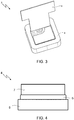
- the microwave antenna module 3 includes the hybrid T/R module 4, which comprises a first package 7 and a second package 8, that are hermetically sealed to one another and that are multilayer ceramic substrate packages.
- said first and second packages 7,8 are metal-ceramic Integral Substrate Packages (ISPs). More preferably, said first and second packages 7,8 are manufactured by using a multilayer ceramic substrate technology, such as LTCC (low temperature cofired ceramics) or HTCC (high temperature cofired ceramics) technology.
- LTCC low temperature cofired ceramics
- HTCC high temperature cofired ceramics
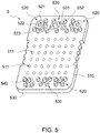
- the hybrid T/R module 4 further comprises the interposer connector 5, that is interposed between said first and second packages 7 and 8, and comprises a body 510 and connection means provided in said body 510.
- First electronic circuitry is arranged within a first hermetic internal cavity of the first package 7, and second electronic circuitry is arranged within a second hermetic internal cavity of the second package 8.
- the first and second electronic circuitries are connected to the connection means of the interposer connector 5 for routing microwave, control and power signals through said connection means.
- the first electronic circuitry includes the directional coupler 6 in stripline-coplanar configuration, which is conveniently based on (i.e., manufactured by using) a multilayer ceramic substrate technology, either LTCC or HTCC, and which is conveniently integrated inside a multilayer ceramic substrate containing the remaining first electronic circuitry.
- connection means of the interposer connector 5 include one or more microwave connection assemblies 520 connected to the first and second electronic circuitries for microwave signals routing between said first and second electronic circuitries.
- Each microwave connection assembly 520 includes:
- the respective first metal element 521 has a rotational symmetry with respect to an axis of symmetry perpendicular to the top and bottom surfaces of the body 510, and the respective second metal elements 523 are arranged, equidistant or in irregularly way, along a circumference, or a semicircumference, or an arc of a circumference, centered on said axis of symmetry.
- said respective second metal elements 523 might be arranged around the respective first dielectric element 522 without following any regular arrangement or specific geometry.
- Each microwave connection assembly 520 implements a transmission line for microwave signals by means of a respective coaxial, semi-coaxial or non-regular configuration formed by the respective first metal element 521, the respective first dielectric element 522 and the respective second metal elements 523. Thence, the microwave connection assemblies 520 can be advantageously used for the routing of microwave signals between the first package 7 and the second package 8.
- first and second metal elements 521,523 may be spring electrical contacts (for example, made of copper-beryllium and coated with gold), ball contacts, fuzz buttons, etc..
- the first dielectric elements 522 may be made of polytetrafluoroethylene (for example, Teflon), or a ceramic material. More in general, the dielectric material used to make the first dielectric elements 522 can be conveniently selected on the basis of the characteristic impedance desired for the transmission lines made by the microwave connection assemblies 520 and of the frequency of the signals to be routed therethrough.
- the microwave antenna module 3 includes also a wide-band antenna 9 (more preferably, a tapered slot antenna, such as a Vivaldi antenna) directly assembled onto the hybrid T/R module 4, in particular mounted on the first package 7.
- the antenna 9 is based on (i.e., is manufactured by using) a ceramic thin film technology.
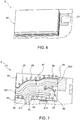
- the directional coupler 6 includes a signal transmission line 61 and a calibration transmission line 62 electromagnetically coupled to each other (in particular, arranged in close proximity to each other so as to be electromagnetically coupled).
- the signal transmission line 61 includes, at a respective first end, a first input/output port 611 and, at a respective second end, a second input/output port 612 connected to the antenna 9.
- the first input/output port 611 is designed to be fed with microwave signals to be radiated by the antenna 9.
- the second input/output port 612 is connected to said antenna 9 to feed the latter with the microwave signals to be radiated, and to receive incoming microwave signals received by said antenna 9.
- the first input/output port 611 is further designed to output the incoming microwave signals.
- the second input/output port 612 is connected to the antenna 9 by means of one of the following RF connection means/technologies:
- the calibration transmission line 62 includes, at a respective first end, a calibration port 621 and, at a respective second end, an isolation port 622, that is coupled to an impedance 63 matching the characteristic impedance of the calibration transmission line 62 (conveniently, the impedance 63 is a 50 Q impedance).
- the directional coupler 6 includes a multilayer structure 60 (conveniently based on multilayer ceramic substrate technology, such as LTCC or HTCC) including dielectric and metal layers stacked on one another.
- a multilayer structure 60 (conveniently based on multilayer ceramic substrate technology, such as LTCC or HTCC) including dielectric and metal layers stacked on one another.
- the signal and calibration transmission lines 61,62 are formed in a first region of one and the same given metal layer of the multilayer structure 60, which given metal layer is interposed between two dielectric layers arranged immediately on and below said given metal layer (in Figure 7 the dielectric layer arranged immediately below said given metal layer being denoted by 64).
- a ground structure 65 is formed in a second region of said given metal layer and is spaced apart from the signal and calibration transmission lines 61 and 62, thereby resulting in said signal and calibration transmission lines 61,62 being arranged on one and the same plane along with the ground structure 65, and in a gap being present between said ground structure 65 and said signal and calibration transmission lines 61 and 62.
- Said gap is filled with a dielectric material (conveniently, the same dielectric material forming the two dielectric layers arranged immediately on and below the given metal layer), which surrounds said signal and calibration transmission lines 61 and 62.
- vias 66 are formed to electrically connect the ground structure 65 to upper and lower metal layers of the multilayer structure 60, thereby resulting in ground planes being arranged above and below the signal and calibration transmission lines 61 and 62.
- said vias 66 extend vertically through the multilayer structure 60, orthogonally to the metal and dielectric layers thereof.
- the signal and calibration transmission lines 61,62 are surrounded by a dielectric with ground planes arranged above and below said signal and calibration transmission lines 61,62, whereby a stripline configuration is implemented. Moreover, the signal and calibration transmission lines 61,62 and the ground structure 65 are arranged on one and the same plane, whereby also a coplanar configuration is implemented. Therefore, the directional coupler 6 has a combined stripline-coplanar configuration.
- connection means of the interposer connector 5 include at least two microwave connection assembly 520, and the first electronic circuitry further includes:
- said transmit/receive switch (or said circulator), said LNA and said HPA are integrated into a Single Chip Front End (SCFE) Monolithic Microwave Integrated Circuit (MMIC). More conveniently, also the directional coupler 6 is integrated into said SCFE MMIC.
- SCFE Single Chip Front End
- MMIC Microwave Integrated Circuit
- the first electronic circuitry may comprise further devices, such as passive electronic components (resistors, capacitors, etc.), active electronic components (for example, semiconductor devices), Surface-Mount Devices (SMDs), etc..
- passive electronic components resistors, capacitors, etc.
- active electronic components for example, semiconductor devices
- SMDs Surface-Mount Devices
- the second electronic circuitry comprises one or more variable phase shifters, one or more attenuators, and one or more amplifiers.
- the second electronic circuitry may comprise also further devices, such as passive electronic components (resistors, capacitors, etc.), active electronic components (for example, semiconductor devices), Surface-Mount Devices (SMDs), etc..
- passive electronic components resistors, capacitors, etc.
- active electronic components for example, semiconductor devices
- SMDs Surface-Mount Devices
- connection means of the interposer connector 5 further include one or more control/power connection assemblies 530 connected to the first and second electronic circuitries for control signals routing between, and/or for power supply to, said first and second electronic circuitries.
- Each control/power connection assemblies 530 includes:
- the control/power connection assemblies 530 implement transmission lines for control signals carrying commands and/or data, and/or for high/low power signals for power supply. Thence, the control/power connection assemblies 530 can be advantageously used for the routing of control and/or power supply signals between the first package 7 and the second package 8.
- the third metal elements 531 may be spring electrical contacts (for example, made of copper-beryllium and coated with gold), ball contacts, fuzz buttons, etc..
- the second dielectric elements 532 may be made of polytetrafluoroethylene (for example, Teflon), or a ceramic material. More in general, also the dielectric material used to make the second dielectric elements 532 can be conveniently selected on the basis of the characteristic impedance desired for the transmission lines made by the control/power connection assemblies 530 and of the frequency of the signals to be routed therethrough.
- connection means of the interposer connector 5 further include one or more fourth metal elements 540 connected to the first and second electronic circuitries for reference/ground voltage routing between said first and second electronic circuitries.
- Each fourth metal element 540 is a member of each fourth metal element 540.
- the fourth metal elements 540 can be advantageously used to route one or more reference/ground voltages between the first and second packages 7,8.
- the fourth metal elements 540 may be spring electrical contacts (for example, made of copper-beryllium and coated with gold), ball contacts, fuzz buttons, etc..
- the body 510 of the interposer connector 5 is:
- the body 510 is made of a multilayer ceramic material, passive electronic components (such as resistors, capacitors, etc.) may conveniently be integrated inside said body 510 to implement predefined signal routing paths.
- passive electronic components such as resistors, capacitors, etc.
- a plurality of through holes 511 with metalized walls are formed in the body 510 of the interposer connector 5, wherein said through holes 511 extend through said body 510 between the top surface and the bottom surface thereof, perpendicularly to said top and bottom surfaces. Said through holes 511 and the respective metalized walls allow to electrically connect the top surface and the bottom surface of the body 510.
- the body 510 of the interposer connector 5 may be conveniently made of metal (such as aluminium coated with nickel and/or gold). In this case, a better electromagnetic shielding between the first electronic circuitry and the second electronic circuitry is achieved. If the body 510 is made of metal, the through holes 511 are not necessary.
- the first and second packages 7,8 are seam-welded to one another, or welded to one another by a solder of gold and tin, or laser-sealed to one another, thereby resulting in said first and second packages 7,8 being hermetically sealed to one another.
- the first and second packages 7,8 include, each, a respective attachment structure made of metal or a ceramic material; conveniently, said respective attachment structure is ring-shaped; more conveniently, said respective attachment structure is made up of one or more gold plated parts, that may be made of one or more metal materials (such as Kovar® or Invar®) or one or more ceramic materials.
- the attachment structures of the first and second packages 7,8 can be conveniently used to seal the hybrid T/R module 4.
- the respective attachment structures may be conveniently glued (for example, by using adhesive materials/means) or welded together (for example, by means of a solder of gold and tin, or by using a laser sealing technique or a seam welding technique).
- the interposer connector 5 is housed, i.e., encapsulated, within a ring-shaped cavity formed by gluing/welding the attachment structures of said first and second packages 7,8.
- these latter may conveniently comprise parts made of diamond-based composites (such as copper-diamond, aluminium-diamond, silver-diamond), or copper-tungsten, or molybdenum, or copper-molybdenum.
- diamond-based composites such as copper-diamond, aluminium-diamond, silver-diamond
- copper-tungsten or molybdenum, or copper-molybdenum.
- one or more of the following devices/means may be arranged/mounted/installed/integrated/housed on/in the interposer connector 5:
- the interposer connector 5 can be advantageously used to arrange/mount/install/integrate/house devices/means for purifying the first and second hermetic internal cavities, for sensing, for electromagnetic optimization, etc..
- first and second packages 7,8 are 3D structures (in particular, rectangular parallelepiped structures) having, each, a substantially rectangular base with base sizes bigger than a respective height
- said first and second packages 7,8 might have shapes and sizes different than the ones shown in Figure 4 (for example, they might conveniently have substantially square bases and/or, each, respective base sizes that are substantially equal to, or even smaller than, the respective height).
- interposer connector 5 is a 3D structure (in particular, a rectangular parallelepiped structure), that has a substantially rectangular base with base sizes bigger than a respective height, and that has beveled corners
- said interposer connector 5 might have a shape and sizes different than the ones shown in Figure 5 (for example, it might conveniently have no beveled corners, or a substantially square base with or without beveled corners, and/or respective base sizes that are substantially equal to, or even smaller than, the respective height).
- the interposer connector 5 might conveniently have base sizes smaller than the ones of the first package 7, and/or said first package 7 might have base sizes that are substantially equal to, or even bigger than, the ones of the second package 8 (in this case, the interposer connector 5 might have base sizes substantially equal to, or smaller than, the ones of the second package 8), and/or the heights of the first and second packages 7,8 and of the interposer connector 5 might be substantially equal to one another.
- Figures 8 and 9 show simulated plots, respectively, of the return loss at the second input/output port 612 of the signal transmission line 61 of the directional coupler 6, and of the far-field radiation pattern of the microwave antenna module 3, for an example of specific configuration operating in X band.
Landscapes
- Engineering & Computer Science (AREA)
- Remote Sensing (AREA)
- Physics & Mathematics (AREA)
- General Physics & Mathematics (AREA)
- Radar, Positioning & Navigation (AREA)
- Computer Networks & Wireless Communication (AREA)
- Astronomy & Astrophysics (AREA)
- Aviation & Aerospace Engineering (AREA)
- Signal Processing (AREA)
- Variable-Direction Aerials And Aerial Arrays (AREA)
- Electromagnetism (AREA)
Applications Claiming Priority (1)
| Application Number | Priority Date | Filing Date | Title |
|---|---|---|---|
| IT102017000086529A IT201700086529A1 (it) | 2017-07-27 | 2017-07-27 | Modulo d'antenna a microonde per applicazioni spaziali comprendente un modulo trasmetti/ricevi ibrido di tipo package su package |
Publications (2)
| Publication Number | Publication Date |
|---|---|
| EP3435111A1 true EP3435111A1 (fr) | 2019-01-30 |
| EP3435111B1 EP3435111B1 (fr) | 2020-03-11 |
Family
ID=60570127
Family Applications (1)
| Application Number | Title | Priority Date | Filing Date |
|---|---|---|---|
| EP18186105.5A Active EP3435111B1 (fr) | 2017-07-27 | 2018-07-27 | Module d'antenne à micro-ondes destiné à des applications spatiales comprenant un module d'émission/réception hybride de type boîtier sur boîtier |
Country Status (3)
| Country | Link |
|---|---|
| US (1) | US10665952B2 (fr) |
| EP (1) | EP3435111B1 (fr) |
| IT (1) | IT201700086529A1 (fr) |
Cited By (2)
| Publication number | Priority date | Publication date | Assignee | Title |
|---|---|---|---|---|
| CN110911836A (zh) * | 2019-12-23 | 2020-03-24 | 航天南湖电子信息技术股份有限公司 | 一种x波段数字相控阵分布式子阵t/r组件馈电电路 |
| TWI741695B (zh) * | 2019-08-16 | 2021-10-01 | 稜研科技股份有限公司 | 天線封裝驗證板 |
Families Citing this family (5)
| Publication number | Priority date | Publication date | Assignee | Title |
|---|---|---|---|---|
| CN112838366B (zh) * | 2020-12-31 | 2024-02-20 | 中国电子科技集团公司第四十三研究所 | 一种多通道表贴式t/r组件 |
| CN113437501B (zh) * | 2021-04-27 | 2023-02-14 | 中国电子科技集团公司第十四研究所 | 一种小型化高集成天线接口模块 |
| CN113203989A (zh) * | 2021-04-29 | 2021-08-03 | 上海航天电子通讯设备研究所 | 正反面pcb基板共面多通道瓦片式收发组件 |
| US12587231B2 (en) * | 2022-08-16 | 2026-03-24 | Infineon Technologies Ag | Broadband high power TRX hybrid implementation |
| CN115529060B (zh) * | 2022-09-22 | 2024-08-23 | 中国电子科技集团公司第十三研究所 | 瓦片式多通道集成天线微波t/r组件 |
Citations (4)
| Publication number | Priority date | Publication date | Assignee | Title |
|---|---|---|---|---|
| US5446464A (en) | 1992-02-11 | 1995-08-29 | Deutsche Aerospace Ag | Transceiver module |
| EP1307078A2 (fr) * | 2001-10-25 | 2003-05-02 | Hitachi, Ltd. | Module de circuit à haute fréquence |
| EP1311072A1 (fr) * | 2000-08-17 | 2003-05-14 | Hitachi, Ltd. | Module d'emetteur et de recepteur |
| US7151502B2 (en) | 2004-12-29 | 2006-12-19 | Tessera, Inc. | Phased antenna array module |
Family Cites Families (3)
| Publication number | Priority date | Publication date | Assignee | Title |
|---|---|---|---|---|
| US10103447B2 (en) * | 2014-06-13 | 2018-10-16 | Nxp Usa, Inc. | Integrated circuit package with radio frequency coupling structure |
| US9620841B2 (en) * | 2014-06-13 | 2017-04-11 | Nxp Usa, Inc. | Radio frequency coupling structure |
| US9887449B2 (en) * | 2014-08-29 | 2018-02-06 | Nxp Usa, Inc. | Radio frequency coupling structure and a method of manufacturing thereof |
-
2017
- 2017-07-27 IT IT102017000086529A patent/IT201700086529A1/it unknown
-
2018
- 2018-07-27 US US16/047,407 patent/US10665952B2/en active Active
- 2018-07-27 EP EP18186105.5A patent/EP3435111B1/fr active Active
Patent Citations (4)
| Publication number | Priority date | Publication date | Assignee | Title |
|---|---|---|---|---|
| US5446464A (en) | 1992-02-11 | 1995-08-29 | Deutsche Aerospace Ag | Transceiver module |
| EP1311072A1 (fr) * | 2000-08-17 | 2003-05-14 | Hitachi, Ltd. | Module d'emetteur et de recepteur |
| EP1307078A2 (fr) * | 2001-10-25 | 2003-05-02 | Hitachi, Ltd. | Module de circuit à haute fréquence |
| US7151502B2 (en) | 2004-12-29 | 2006-12-19 | Tessera, Inc. | Phased antenna array module |
Non-Patent Citations (2)
| Title |
|---|
| A. FINA ET AL.: "An Advanced Transmit/Receive 3D Ceramic Hybrid Circuit Module for Space Applications", 2015 EUROPEAN MICROWAVE CONFERENCE (EUMC, 7 September 2015 (2015-09-07), pages 785 - 788, XP032823025, DOI: doi:10.1109/EuMC.2015.7345881 |
| FINA ANTONIO ET AL: "An advanced transmit/receive 3D ceramic hybrid circuit module for space applications", 2015 EUROPEAN MICROWAVE CONFERENCE (EUMC), EUMA, 7 September 2015 (2015-09-07), pages 785 - 788, XP032823025, DOI: 10.1109/EUMC.2015.7345881 * |
Cited By (3)
| Publication number | Priority date | Publication date | Assignee | Title |
|---|---|---|---|---|
| TWI741695B (zh) * | 2019-08-16 | 2021-10-01 | 稜研科技股份有限公司 | 天線封裝驗證板 |
| CN110911836A (zh) * | 2019-12-23 | 2020-03-24 | 航天南湖电子信息技术股份有限公司 | 一种x波段数字相控阵分布式子阵t/r组件馈电电路 |
| CN110911836B (zh) * | 2019-12-23 | 2021-10-26 | 航天南湖电子信息技术股份有限公司 | 一种x波段数字相控阵分布式子阵t/r组件馈电电路 |
Also Published As
| Publication number | Publication date |
|---|---|
| IT201700086529A1 (it) | 2019-01-27 |
| US20190067824A1 (en) | 2019-02-28 |
| EP3435111B1 (fr) | 2020-03-11 |
| US10665952B2 (en) | 2020-05-26 |
Similar Documents
| Publication | Publication Date | Title |
|---|---|---|
| EP3435111B1 (fr) | Module d'antenne à micro-ondes destiné à des applications spatiales comprenant un module d'émission/réception hybride de type boîtier sur boîtier | |
| KR102466972B1 (ko) | 스위칭 가능한 송수신 페이즈드 어레이 안테나 | |
| US11658390B2 (en) | Wireless communications package with integrated antenna array | |
| US9819098B2 (en) | Antenna-in-package structures with broadside and end-fire radiations | |
| CN109792109B (zh) | 天线元件 | |
| US7119745B2 (en) | Apparatus and method for constructing and packaging printed antenna devices | |
| EP1515389B1 (fr) | Composant HF multi-couches à antenne plane et procédé de fabrication associé | |
| US6512431B2 (en) | Millimeterwave module compact interconnect | |
| US20150257254A1 (en) | High-frequency circuit package and sensor module | |
| US10854984B2 (en) | Air-filled quad-ridge radiator for AESA applications | |
| US9252497B2 (en) | Hybrid single aperture inclined antenna | |
| EP2575167B1 (fr) | Dispositif électronique | |
| KR20120078697A (ko) | 정밀 도파관 인터페이스 | |
| US11233303B2 (en) | High frequency filter | |
| JP4658535B2 (ja) | 高周波モジュール | |
| Oppermann et al. | Multifunctional MMICs–key enabler for future AESA panel arrays | |
| Oppermann et al. | RF modules (Tx-Rx) with multifunctional MMICs | |
| CN116613507A (zh) | 一种星载可扩展高密度多波束有源阵列的实现方法 | |
| KR102717918B1 (ko) | 리액티브 어레이 | |
| JP2025500198A (ja) | レーダセンサ用高周波モジュール | |
| Edward et al. | W-band active transmit and receive phased array antennas | |
| JP2000133735A (ja) | 高周波集積回路用外囲器 |
Legal Events
| Date | Code | Title | Description |
|---|---|---|---|
| PUAI | Public reference made under article 153(3) epc to a published international application that has entered the european phase |
Free format text: ORIGINAL CODE: 0009012 |
|
| STAA | Information on the status of an ep patent application or granted ep patent |
Free format text: STATUS: THE APPLICATION HAS BEEN PUBLISHED |
|
| AK | Designated contracting states |
Kind code of ref document: A1 Designated state(s): AL AT BE BG CH CY CZ DE DK EE ES FI FR GB GR HR HU IE IS IT LI LT LU LV MC MK MT NL NO PL PT RO RS SE SI SK SM TR |
|
| AX | Request for extension of the european patent |
Extension state: BA ME |
|
| STAA | Information on the status of an ep patent application or granted ep patent |
Free format text: STATUS: REQUEST FOR EXAMINATION WAS MADE |
|
| 17P | Request for examination filed |
Effective date: 20190729 |
|
| RBV | Designated contracting states (corrected) |
Designated state(s): AL AT BE BG CH CY CZ DE DK EE ES FI FR GB GR HR HU IE IS IT LI LT LU LV MC MK MT NL NO PL PT RO RS SE SI SK SM TR |
|
| RIC1 | Information provided on ipc code assigned before grant |
Ipc: H01P 3/06 20060101ALI20190822BHEP Ipc: H01Q 3/26 20060101ALI20190822BHEP Ipc: G01S 7/40 20060101ALI20190822BHEP Ipc: H01Q 1/28 20060101ALI20190822BHEP Ipc: H01Q 19/17 20060101ALI20190822BHEP Ipc: H01P 3/12 20060101ALI20190822BHEP Ipc: H01P 5/18 20060101ALI20190822BHEP Ipc: H05K 5/06 20060101ALI20190822BHEP Ipc: H01Q 13/08 20060101ALI20190822BHEP Ipc: G01S 7/02 20060101ALN20190822BHEP Ipc: H04B 7/185 20060101ALI20190822BHEP Ipc: H01P 3/00 20060101ALI20190822BHEP Ipc: G01S 13/02 20060101ALI20190822BHEP Ipc: G01S 7/03 20060101AFI20190822BHEP |
|
| GRAP | Despatch of communication of intention to grant a patent |
Free format text: ORIGINAL CODE: EPIDOSNIGR1 |
|
| STAA | Information on the status of an ep patent application or granted ep patent |
Free format text: STATUS: GRANT OF PATENT IS INTENDED |
|
| INTG | Intention to grant announced |
Effective date: 20191002 |
|
| RIN1 | Information on inventor provided before grant (corrected) |
Inventor name: DI CARLOFELICE, ALESSANDRO Inventor name: DE PAULIS, FRANCESCO Inventor name: SURIANI, ANDREA Inventor name: TOGNOLATTI, PIERO Inventor name: ORLANDI, ANTONIO Inventor name: FINA, ANTONIO Inventor name: DI MARCANTONIO, ULISSE |
|
| GRAS | Grant fee paid |
Free format text: ORIGINAL CODE: EPIDOSNIGR3 |
|
| GRAA | (expected) grant |
Free format text: ORIGINAL CODE: 0009210 |
|
| STAA | Information on the status of an ep patent application or granted ep patent |
Free format text: STATUS: THE PATENT HAS BEEN GRANTED |
|
| AK | Designated contracting states |
Kind code of ref document: B1 Designated state(s): AL AT BE BG CH CY CZ DE DK EE ES FI FR GB GR HR HU IE IS IT LI LT LU LV MC MK MT NL NO PL PT RO RS SE SI SK SM TR |
|
| REG | Reference to a national code |
Ref country code: GB Ref legal event code: FG4D |
|
| RIN1 | Information on inventor provided before grant (corrected) |
Inventor name: SURIANI, ANDREA Inventor name: DE PAULIS, FRANCESCO Inventor name: FINA, ANTONIO Inventor name: DI MARCANTONIO, ULISSE Inventor name: DI CARLOFELICE, ALESSANDRO Inventor name: TOGNOLATTI, PIERO Inventor name: ORLANDI, ANTONIO |
|
| REG | Reference to a national code |
Ref country code: CH Ref legal event code: EP |
|
| REG | Reference to a national code |
Ref country code: AT Ref legal event code: REF Ref document number: 1243841 Country of ref document: AT Kind code of ref document: T Effective date: 20200315 |
|
| REG | Reference to a national code |
Ref country code: DE Ref legal event code: R096 Ref document number: 602018002969 Country of ref document: DE |
|
| REG | Reference to a national code |
Ref country code: IE Ref legal event code: FG4D |
|
| REG | Reference to a national code |
Ref country code: NL Ref legal event code: FP |
|
| PG25 | Lapsed in a contracting state [announced via postgrant information from national office to epo] |
Ref country code: RS Free format text: LAPSE BECAUSE OF FAILURE TO SUBMIT A TRANSLATION OF THE DESCRIPTION OR TO PAY THE FEE WITHIN THE PRESCRIBED TIME-LIMIT Effective date: 20200311 Ref country code: FI Free format text: LAPSE BECAUSE OF FAILURE TO SUBMIT A TRANSLATION OF THE DESCRIPTION OR TO PAY THE FEE WITHIN THE PRESCRIBED TIME-LIMIT Effective date: 20200311 Ref country code: NO Free format text: LAPSE BECAUSE OF FAILURE TO SUBMIT A TRANSLATION OF THE DESCRIPTION OR TO PAY THE FEE WITHIN THE PRESCRIBED TIME-LIMIT Effective date: 20200611 |
|
| PG25 | Lapsed in a contracting state [announced via postgrant information from national office to epo] |
Ref country code: SE Free format text: LAPSE BECAUSE OF FAILURE TO SUBMIT A TRANSLATION OF THE DESCRIPTION OR TO PAY THE FEE WITHIN THE PRESCRIBED TIME-LIMIT Effective date: 20200311 Ref country code: LV Free format text: LAPSE BECAUSE OF FAILURE TO SUBMIT A TRANSLATION OF THE DESCRIPTION OR TO PAY THE FEE WITHIN THE PRESCRIBED TIME-LIMIT Effective date: 20200311 Ref country code: BG Free format text: LAPSE BECAUSE OF FAILURE TO SUBMIT A TRANSLATION OF THE DESCRIPTION OR TO PAY THE FEE WITHIN THE PRESCRIBED TIME-LIMIT Effective date: 20200611 Ref country code: GR Free format text: LAPSE BECAUSE OF FAILURE TO SUBMIT A TRANSLATION OF THE DESCRIPTION OR TO PAY THE FEE WITHIN THE PRESCRIBED TIME-LIMIT Effective date: 20200612 Ref country code: HR Free format text: LAPSE BECAUSE OF FAILURE TO SUBMIT A TRANSLATION OF THE DESCRIPTION OR TO PAY THE FEE WITHIN THE PRESCRIBED TIME-LIMIT Effective date: 20200311 |
|
| REG | Reference to a national code |
Ref country code: LT Ref legal event code: MG4D |
|
| PG25 | Lapsed in a contracting state [announced via postgrant information from national office to epo] |
Ref country code: RO Free format text: LAPSE BECAUSE OF FAILURE TO SUBMIT A TRANSLATION OF THE DESCRIPTION OR TO PAY THE FEE WITHIN THE PRESCRIBED TIME-LIMIT Effective date: 20200311 Ref country code: SK Free format text: LAPSE BECAUSE OF FAILURE TO SUBMIT A TRANSLATION OF THE DESCRIPTION OR TO PAY THE FEE WITHIN THE PRESCRIBED TIME-LIMIT Effective date: 20200311 Ref country code: IS Free format text: LAPSE BECAUSE OF FAILURE TO SUBMIT A TRANSLATION OF THE DESCRIPTION OR TO PAY THE FEE WITHIN THE PRESCRIBED TIME-LIMIT Effective date: 20200711 Ref country code: SM Free format text: LAPSE BECAUSE OF FAILURE TO SUBMIT A TRANSLATION OF THE DESCRIPTION OR TO PAY THE FEE WITHIN THE PRESCRIBED TIME-LIMIT Effective date: 20200311 Ref country code: PT Free format text: LAPSE BECAUSE OF FAILURE TO SUBMIT A TRANSLATION OF THE DESCRIPTION OR TO PAY THE FEE WITHIN THE PRESCRIBED TIME-LIMIT Effective date: 20200805 Ref country code: EE Free format text: LAPSE BECAUSE OF FAILURE TO SUBMIT A TRANSLATION OF THE DESCRIPTION OR TO PAY THE FEE WITHIN THE PRESCRIBED TIME-LIMIT Effective date: 20200311 Ref country code: CZ Free format text: LAPSE BECAUSE OF FAILURE TO SUBMIT A TRANSLATION OF THE DESCRIPTION OR TO PAY THE FEE WITHIN THE PRESCRIBED TIME-LIMIT Effective date: 20200311 Ref country code: LT Free format text: LAPSE BECAUSE OF FAILURE TO SUBMIT A TRANSLATION OF THE DESCRIPTION OR TO PAY THE FEE WITHIN THE PRESCRIBED TIME-LIMIT Effective date: 20200311 |
|
| REG | Reference to a national code |
Ref country code: AT Ref legal event code: MK05 Ref document number: 1243841 Country of ref document: AT Kind code of ref document: T Effective date: 20200311 |
|
| REG | Reference to a national code |
Ref country code: DE Ref legal event code: R097 Ref document number: 602018002969 Country of ref document: DE |
|
| PLBE | No opposition filed within time limit |
Free format text: ORIGINAL CODE: 0009261 |
|
| STAA | Information on the status of an ep patent application or granted ep patent |
Free format text: STATUS: NO OPPOSITION FILED WITHIN TIME LIMIT |
|
| PG25 | Lapsed in a contracting state [announced via postgrant information from national office to epo] |
Ref country code: AT Free format text: LAPSE BECAUSE OF FAILURE TO SUBMIT A TRANSLATION OF THE DESCRIPTION OR TO PAY THE FEE WITHIN THE PRESCRIBED TIME-LIMIT Effective date: 20200311 Ref country code: DK Free format text: LAPSE BECAUSE OF FAILURE TO SUBMIT A TRANSLATION OF THE DESCRIPTION OR TO PAY THE FEE WITHIN THE PRESCRIBED TIME-LIMIT Effective date: 20200311 Ref country code: ES Free format text: LAPSE BECAUSE OF FAILURE TO SUBMIT A TRANSLATION OF THE DESCRIPTION OR TO PAY THE FEE WITHIN THE PRESCRIBED TIME-LIMIT Effective date: 20200311 |
|
| 26N | No opposition filed |
Effective date: 20201214 |
|
| PG25 | Lapsed in a contracting state [announced via postgrant information from national office to epo] |
Ref country code: MC Free format text: LAPSE BECAUSE OF FAILURE TO SUBMIT A TRANSLATION OF THE DESCRIPTION OR TO PAY THE FEE WITHIN THE PRESCRIBED TIME-LIMIT Effective date: 20200311 Ref country code: PL Free format text: LAPSE BECAUSE OF FAILURE TO SUBMIT A TRANSLATION OF THE DESCRIPTION OR TO PAY THE FEE WITHIN THE PRESCRIBED TIME-LIMIT Effective date: 20200311 Ref country code: SI Free format text: LAPSE BECAUSE OF FAILURE TO SUBMIT A TRANSLATION OF THE DESCRIPTION OR TO PAY THE FEE WITHIN THE PRESCRIBED TIME-LIMIT Effective date: 20200311 |
|
| REG | Reference to a national code |
Ref country code: BE Ref legal event code: MM Effective date: 20200731 |
|
| PG25 | Lapsed in a contracting state [announced via postgrant information from national office to epo] |
Ref country code: LU Free format text: LAPSE BECAUSE OF NON-PAYMENT OF DUE FEES Effective date: 20200727 |
|
| PG25 | Lapsed in a contracting state [announced via postgrant information from national office to epo] |
Ref country code: BE Free format text: LAPSE BECAUSE OF NON-PAYMENT OF DUE FEES Effective date: 20200731 |
|
| PG25 | Lapsed in a contracting state [announced via postgrant information from national office to epo] |
Ref country code: IE Free format text: LAPSE BECAUSE OF NON-PAYMENT OF DUE FEES Effective date: 20200727 |
|
| REG | Reference to a national code |
Ref country code: CH Ref legal event code: PL |
|
| PG25 | Lapsed in a contracting state [announced via postgrant information from national office to epo] |
Ref country code: LI Free format text: LAPSE BECAUSE OF NON-PAYMENT OF DUE FEES Effective date: 20210731 Ref country code: CH Free format text: LAPSE BECAUSE OF NON-PAYMENT OF DUE FEES Effective date: 20210731 |
|
| PG25 | Lapsed in a contracting state [announced via postgrant information from national office to epo] |
Ref country code: TR Free format text: LAPSE BECAUSE OF FAILURE TO SUBMIT A TRANSLATION OF THE DESCRIPTION OR TO PAY THE FEE WITHIN THE PRESCRIBED TIME-LIMIT Effective date: 20200311 Ref country code: MT Free format text: LAPSE BECAUSE OF FAILURE TO SUBMIT A TRANSLATION OF THE DESCRIPTION OR TO PAY THE FEE WITHIN THE PRESCRIBED TIME-LIMIT Effective date: 20200311 Ref country code: CY Free format text: LAPSE BECAUSE OF FAILURE TO SUBMIT A TRANSLATION OF THE DESCRIPTION OR TO PAY THE FEE WITHIN THE PRESCRIBED TIME-LIMIT Effective date: 20200311 |
|
| PG25 | Lapsed in a contracting state [announced via postgrant information from national office to epo] |
Ref country code: MK Free format text: LAPSE BECAUSE OF FAILURE TO SUBMIT A TRANSLATION OF THE DESCRIPTION OR TO PAY THE FEE WITHIN THE PRESCRIBED TIME-LIMIT Effective date: 20200311 Ref country code: AL Free format text: LAPSE BECAUSE OF FAILURE TO SUBMIT A TRANSLATION OF THE DESCRIPTION OR TO PAY THE FEE WITHIN THE PRESCRIBED TIME-LIMIT Effective date: 20200311 |
|
| P01 | Opt-out of the competence of the unified patent court (upc) registered |
Effective date: 20230518 |
|
| PGFP | Annual fee paid to national office [announced via postgrant information from national office to epo] |
Ref country code: NL Payment date: 20250724 Year of fee payment: 8 |
|
| PGFP | Annual fee paid to national office [announced via postgrant information from national office to epo] |
Ref country code: DE Payment date: 20250728 Year of fee payment: 8 |
|
| PGFP | Annual fee paid to national office [announced via postgrant information from national office to epo] |
Ref country code: IT Payment date: 20250627 Year of fee payment: 8 |
|
| PGFP | Annual fee paid to national office [announced via postgrant information from national office to epo] |
Ref country code: GB Payment date: 20250722 Year of fee payment: 8 |
|
| PGFP | Annual fee paid to national office [announced via postgrant information from national office to epo] |
Ref country code: FR Payment date: 20250725 Year of fee payment: 8 |