EP3435741A1 - Laminierte reflektierende elektrodenfolie, laminiertes reflektierendes elektrodenmuster und verfahren zur herstellung des laminierten reflektierenden elektrodenmusters - Google Patents
Laminierte reflektierende elektrodenfolie, laminiertes reflektierendes elektrodenmuster und verfahren zur herstellung des laminierten reflektierenden elektrodenmusters Download PDFInfo
- Publication number
- EP3435741A1 EP3435741A1 EP17770251.1A EP17770251A EP3435741A1 EP 3435741 A1 EP3435741 A1 EP 3435741A1 EP 17770251 A EP17770251 A EP 17770251A EP 3435741 A1 EP3435741 A1 EP 3435741A1
- Authority
- EP
- European Patent Office
- Prior art keywords
- film
- balance
- reflection electrode
- multilayer reflection
- transparent conductive
- Prior art date
- Legal status (The legal status is an assumption and is not a legal conclusion. Google has not performed a legal analysis and makes no representation as to the accuracy of the status listed.)
- Granted
Links
Images
Classifications
-
- H—ELECTRICITY
- H01—ELECTRIC ELEMENTS
- H01B—CABLES; CONDUCTORS; INSULATORS; SELECTION OF MATERIALS FOR THEIR CONDUCTIVE, INSULATING OR DIELECTRIC PROPERTIES
- H01B1/00—Conductors or conductive bodies characterised by the conductive materials; Selection of materials as conductors
- H01B1/02—Conductors or conductive bodies characterised by the conductive materials; Selection of materials as conductors mainly consisting of metals or alloys
-
- H—ELECTRICITY
- H05—ELECTRIC TECHNIQUES NOT OTHERWISE PROVIDED FOR
- H05B—ELECTRIC HEATING; ELECTRIC LIGHT SOURCES NOT OTHERWISE PROVIDED FOR; CIRCUIT ARRANGEMENTS FOR ELECTRIC LIGHT SOURCES, IN GENERAL
- H05B33/00—Electroluminescent light sources
- H05B33/10—Apparatus or processes specially adapted to the manufacture of electroluminescent light sources
-
- H—ELECTRICITY
- H05—ELECTRIC TECHNIQUES NOT OTHERWISE PROVIDED FOR
- H05B—ELECTRIC HEATING; ELECTRIC LIGHT SOURCES NOT OTHERWISE PROVIDED FOR; CIRCUIT ARRANGEMENTS FOR ELECTRIC LIGHT SOURCES, IN GENERAL
- H05B33/00—Electroluminescent light sources
- H05B33/12—Light sources with substantially two-dimensional [2D] radiating surfaces
- H05B33/26—Light sources with substantially two-dimensional [2D] radiating surfaces characterised by the composition or arrangement of the conductive material used as an electrode
-
- H—ELECTRICITY
- H10—SEMICONDUCTOR DEVICES; ELECTRIC SOLID-STATE DEVICES NOT OTHERWISE PROVIDED FOR
- H10K—ORGANIC ELECTRIC SOLID-STATE DEVICES
- H10K50/00—Organic light-emitting devices
-
- H—ELECTRICITY
- H10—SEMICONDUCTOR DEVICES; ELECTRIC SOLID-STATE DEVICES NOT OTHERWISE PROVIDED FOR
- H10K—ORGANIC ELECTRIC SOLID-STATE DEVICES
- H10K50/00—Organic light-emitting devices
- H10K50/80—Constructional details
- H10K50/805—Electrodes
- H10K50/81—Anodes
- H10K50/818—Reflective anodes, e.g. ITO combined with thick metallic layers
-
- H—ELECTRICITY
- H10—SEMICONDUCTOR DEVICES; ELECTRIC SOLID-STATE DEVICES NOT OTHERWISE PROVIDED FOR
- H10K—ORGANIC ELECTRIC SOLID-STATE DEVICES
- H10K59/00—Integrated devices, or assemblies of multiple devices, comprising at least one organic light-emitting element covered by group H10K50/00
- H10K59/80—Constructional details
- H10K59/805—Electrodes
- H10K59/8051—Anodes
- H10K59/80518—Reflective anodes, e.g. ITO combined with thick metallic layers
-
- H—ELECTRICITY
- H10—SEMICONDUCTOR DEVICES; ELECTRIC SOLID-STATE DEVICES NOT OTHERWISE PROVIDED FOR
- H10K—ORGANIC ELECTRIC SOLID-STATE DEVICES
- H10K71/00—Manufacture or treatment specially adapted for the organic devices covered by this subclass
-
- H—ELECTRICITY
- H10—SEMICONDUCTOR DEVICES; ELECTRIC SOLID-STATE DEVICES NOT OTHERWISE PROVIDED FOR
- H10K—ORGANIC ELECTRIC SOLID-STATE DEVICES
- H10K71/00—Manufacture or treatment specially adapted for the organic devices covered by this subclass
- H10K71/60—Forming conductive regions or layers, e.g. electrodes
-
- H—ELECTRICITY
- H10—SEMICONDUCTOR DEVICES; ELECTRIC SOLID-STATE DEVICES NOT OTHERWISE PROVIDED FOR
- H10K—ORGANIC ELECTRIC SOLID-STATE DEVICES
- H10K2102/00—Constructional details relating to the organic devices covered by this subclass
Definitions
- the present disclosure relates to a multilayer reflection electrode film that can be used as, for example, an anode of an organic electroluminescence (EL) element, a multilayer reflection electrode pattern formed of the multilayer reflection electrode film, and a method of forming the multilayer reflection electrode pattern.
- EL organic electroluminescence
- an organic EL display is formed of organic EL elements arranged on a transparent substrate.
- An organic EL element includes an anode, an organic EL light emitting layer, and a cathode that are formed on a transparent substrate in a predetermined pattern and is a light emitting element that uses a principle in which light is emitted when holes and electrons are injected into the organic EL layer from the anode and the cathode, respectively, and are combined with each other in the organic EL light emitting layer.
- a bottom emission type of extracting light from the transparent substrate side and a top emission type of extracting light from a side opposite to the transparent substrate are known.
- the top emission type has a higher aperture ratio than the bottom emission type, and thus is advantageous in increasing luminance.
- the anode used in the top emission type organic EL element is desired to have a reflectance that is high in order to efficiently extract light generated from the electroluminescence layer to the outside; a high conductivity; and a work function that is sufficiently high such that holes can be efficiently injected into the electroluminescence layer.
- Patent Documents 1 and 2 a multilayer film in which a work function is increased by performing an oxygen plasma treatment or the like on a surface of a metal film to form a surface oxide film is used as an anode of an organic EL element.
- Patent Documents 3, 4, and 5 a multilayer film in which a transparent conductive film such as an ITO film is formed on a surface of a metal film is used as an electrode of an organic EL element. Further, in Patent Document 6, a surface-modified ITO film in which a work function is increased by irradiating a surface of an ITO film with oxygen ions or electrons to modify the surface is used as an anode of an organic EL element.
- Patent Document 7 describes that zinc oxide (ZnO), aluminum-doped zinc oxide (AZO), or gallium-doped zinc oxide (GZO) is used as a metal oxide in a multilayer film in which a metal oxide thin film is laminated on a conductive layer including Ag as a major component.
- ZnO zinc oxide
- AZO aluminum-doped zinc oxide
- GZO gallium-doped zinc oxide
- a metal oxide including ZnO is likely to be dissolved in a resist remover (weak alkali) used in an etching method. Therefore, it is difficult to form a fine electrode pattern in which a multilayer film using a metal oxide including ZnO such as AZO or GZO is used as an electrode for an organic EL display through an etching method.
- Non-Patent Document 1 " Technology of Transparent Conductive Films (Second Revised Edition)", p. 171-172, JAPANESE SOCIETY FOR THE PROMOTION OF SCIENCE The 166th Committee on Photonic and Electronic Oxide, Ohmsha Ltd., Second Edition First Printing, December 20, 2006
- the multilayer reflection electrode film is required to have low electrical resistance and high reflectance equivalent to those of pure silver.
- it is required to enable the easy formation of a fine electrode pattern formed of a multilayer reflection electrode film using an etching method.
- the reflectance may decrease and the resistivity may increase due to damage by the oxygen plasma treatment.
- sulfur resistance is insufficient, and thus the reflectance may decrease and the resistivity may increase during use in the atmosphere.
- the reflectance of visible light in particular, the reflectance of light in a blue wavelength range (400 to 500 nm) may decrease.
- the surface of the ITO film is irradiated with oxygen ions or electrons to modify the surface as described in Patent Document 6, the surface of the ITO film is roughened such that light may be scattered.
- the etching rate of the Ag alloy film is higher than that of the ITO film. Therefore, in a case where the Ag alloy film and the ITO film are collectively etched using the same etchant, the Ag alloy film may be over-etched, or ITO film residues may remain.
- the present disclosure has been made in consideration of the above-described circumstances, and an object thereof is to provide: a multilayer reflection electrode film having a high reflectance in a visible range, in particular, in a blue wavelength range and having a low resistance value with which a fine electrode pattern can be easily formed using an etching method; a multilayer reflection electrode pattern formed of the multilayer reflection electrode film; and a method of forming the multilayer reflection electrode pattern.
- a multilayer reflection electrode film including: a Ag film that is formed of Ag or an Ag alloy; and a transparent conductive oxide film that is disposed on the Ag film, in which the transparent conductive oxide film is formed of an oxide that includes Zn and Ga and further includes one element or two or more elements selected from the group consisting of Sn, Y, and Ti.
- the multilayer reflection electrode film according to the present disclosure includes the Ag film, and thus has low electrical resistance.
- the transparent conductive oxide film formed of the oxide that includes Zn and Ga and further includes one element or two or more elements selected from the group consisting of Sn, Y, and Ti is disposed on the Ag film. Therefore, the reflectance in a visible light, in particular, in a blue wavelength range is high. The reason for this is presumed to be that a refractive index of the transparent conductive oxide film in the visible range, in particular, in the blue wavelength range, is lower than that of other transparent conductive oxides such as ITO.
- the transparent conductive oxide film further includes one element or two or more elements selected from the group consisting of Sn, Y, and Ti. Therefore, alkali resistance is improved, and the transparent conductive oxide film is not likely to be dissolved in an alkaline resist remover. Therefore, with the multilayer reflection electrode film according to the present disclosure, an electrode pattern can be formed using an etching method.
- the difference in etching rate is small. Accordingly, in a case where an electrode pattern is formed using an etching method with the multilayer reflection electrode film according to the present disclosure, the amount of over-etching is small.
- the transparent conductive oxide film has a higher work function than ITO and thus can also be used without modifying the surface by irradiation of oxygen ions or electrons.
- atomic proportions with respect to all the metal elements included in the transparent conductive oxide film are Ga: 0.5 at% to 30.0 at%, each of Sn, Y, and Ti: 0.1 at% to 10.0 at%, and a balance of Zn.
- the Ga content with respect to all the metal elements included in the transparent conductive oxide film is in a range of 0.5 at% to 30.0 at%. Therefore, adhesiveness between the Ag film and the transparent conductive oxide film can be improved while preventing an increase in electrical resistance.
- each of the contents of Sn, Y, and Ti is in a range of 0.1 at% to 10.0 at%. Therefore, alkali resistance and environment resistance can be improved while preventing an increase in electrical resistance. Further, in order to further improve the effect of improving alkali resistance, it is more preferable that the transparent conductive oxide film 13 further includes Y.
- atomic proportions with respect to all the metal elements included in the transparent conductive oxide film are Ga: 0.5 at% to 18.0 at%, each of Sn, Y, and Ti: 0.1 at% to 10.0 at%, and a balance of Zn.
- the Ga content with respect to all the metal elements included in the transparent conductive oxide film is in a range of 0.5 at% to 18.0 at%. Therefore, adhesiveness between the Ag film and the transparent conductive oxide film can be further improved while further preventing an increase in electrical resistance.
- each of the contents of Sn, Y, and Ti is in a range of 0.1 at% to 10.0 at%. Therefore, alkali resistance and environment resistance can be improved while preventing an increase in electrical resistance.
- atomic proportions with respect to all the metal elements included in the transparent conductive oxide film are Ga: 0.5 at% to 14.0 at%, each of Sn, Y, and Ti: 0.1 at% to 10.0 at%, and a balance of Zn.
- the Ga content with respect to all the metal elements included in the transparent conductive oxide film is in a range of 0.5 at% to 14.0 at%. Therefore, adhesiveness between the Ag film and the transparent conductive oxide film can be further improved while further preventing an increase in electrical resistance.
- each of the contents of Sn, Y, and Ti is in a range of 0.1 at% to 10.0 at%. Therefore, alkali resistance and environment resistance can be improved while preventing an increase in electrical resistance.
- the Ag film is formed of an Ag alloy including 0.2 at% to 2.0 at% of one element or two or more elements in total selected from the group consisting of Cu, In, Sn, Sb, Ti, Mg, Zn, Ge, Al, Ga, Pd, Au, Pt, Bi, Mn, Sc, Y, Nd, Sm, Eu, Gd, Tb, and Er and a balance of Ag and inevitable impurities.
- the Ag film includes one element or two or more elements in total selected from the group consisting of Cu, In, Sn, Sb, Ti, Mg, Zn, Ge, Al, Ga, Pd, Au, Pt, Bi, Mn, Sc, Y, Nd, Sm, Eu, Gd, Tb, and Er and a balance of Ag and inevitable impurities. Therefore, sulfur resistance, heat resistance, or the like of the Ag film can be improved, and deterioration can be prevented. As a result, the Ag film can be stably used for a long period of time.
- a thickness of the Ag film is 50 nm or more, and it is preferable that a thickness of the transparent conductive oxide film is 100 nm or less.
- the thickness of the Ag film is 50 nm or more. Therefore, the amount of visible light reflected from the surface of the Ag film increases, and the reflectance of visible light is improved.
- the thickness of the transparent conductive oxide film is 100 nm or less. Therefore, the transmittance of visible light in the transparent conductive oxide film is improved, and the amount of visible light reflected from the surface of the Ag film increases
- a multilayer reflection electrode pattern is provided that is formed of the above-described multilayer reflection electrode film, the multilayer reflection electrode pattern including a predetermined pattern.
- the multilayer reflection electrode pattern according to the present disclosure is formed of the above-described multilayer reflection electrode film. Therefore, the electrical resistance is low, and the reflectance of visible light, in particular, light in a blue wavelength range is high.
- a method of forming the multilayer reflection electrode pattern including: a multilayer reflection electrode film forming step of forming the multilayer reflection electrode film including the Ag film and the transparent conductive oxide film on a film forming surface of a base material; a resist film forming step of forming a resist film having a predetermined pattern shape on the multilayer reflection electrode film; an etching step of collectively etching the multilayer reflection electrode film on which the resist film is formed by using an acidic mixed solution including phosphoric acid and acetic acid as an etchant; and a resist film removing step of removing the resist film after etching.
- the method of forming the multilayer reflection electrode pattern having the above-described configuration in a case where the acidic mixed solution including phosphoric acid and acetic acid is used as an etchant, a difference in etching rate between the Ag film and the transparent conductive oxide film is small. Therefore, even in a case where the multilayer reflection electrode film is collectively etched, the over-etching of the Ag film or the remaining of residues of the transparent conductive oxide film can be prevented, and the electrode pattern can be accurately formed.
- alkali resistance of the transparent conductive oxide film is improved due to the addition of one element or two or more elements selected from the group consisting of Sn, Y, and Ti. Therefore, even in a case where the resist film is removed using the alkaline resist remover in the resist film removing step, deterioration of the characteristics of the multilayer reflection electrode pattern can be prevented.
- a method of forming the multilayer reflection electrode pattern including: a resist film forming step of forming a resist film having a reverse pattern shape of the predetermined pattern on a film forming surface of a base material; a multilayer reflection electrode film forming step of forming the multilayer reflection electrode film including the Ag film and the transparent conductive oxide film on the film forming surface of the base material on which the resist film is formed; and a resist film removing step of removing the resist film.
- the resist film is formed on the film forming surface of the base material in a reverse pattern shape of the predetermined pattern, and the multilayer reflection electrode film is formed on the film forming surface of the base material on which the resist film is formed.
- the multilayer reflection electrode film remains only in a region the resist film is not formed, and the multilayer reflection electrode pattern including the predetermined pattern can be formed. Therefore, it is not necessary to perform the etching step, and the predetermined pattern can be accurately formed.
- alkali resistance of the transparent conductive oxide film is improved due to the addition of one element or two or more elements selected from the group consisting of Sn, Y, and Ti. Therefore, even in a case where the resist film is removed using the alkaline resist remover in the resist film removing step, deterioration of the characteristics of the multilayer reflection electrode pattern can be prevented.
- a multilayer reflection electrode film having a high reflectance in a visible range, in particular, in a blue wavelength range and having a low resistance value with which a fine electrode pattern can be easily formed using an etching method a multilayer reflection electrode pattern formed of the multilayer reflection electrode film; and a method of forming the multilayer reflection electrode pattern.
- a multilayer reflection electrode film 10 according to the embodiment is used as an anode of an organic EL element and particularly is used as an anode of a top emission type organic EL element.
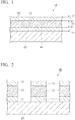
- the multilayer reflection electrode film 10 is shown in FIG. 1 .
- the multilayer reflection electrode film 10 includes: an underlayer oxide film 11 that is formed as an underlayer on one surface of a substrate 20 as a base material; a Ag film 12 that is formed on the underlayer oxide film 11; and a transparent conductive oxide film 13 that is formed on the Ag film 12.
- a substrate 20 for example, a glass substrate or a resin film can be used.
- the reflectance in a visible range, in particular, in a blue wavelength range is high, and the resistance value is low.
- the average reflectance of the multilayer reflection electrode film 10 in a visible range is preferably 95% or higher and more preferably 96% or higher.
- the average reflectance of the multilayer reflection electrode film 10 in a blue wavelength range is preferably 86% or higher and more preferably 88% or higher. The higher the average transmittance, the better. Therefore, the upper limit value is not particularly limited.
- the reflectance in a visible range is preferably 99% or lower and more preferably 98% or lower.
- the reflectance in a blue wavelength range is preferably 95% or lower and more preferably 90% or lower.
- the sheet resistance value of multilayer reflection electrode film 10 is preferably 1.0 ⁇ /sq. or lower and more preferably 0.5 ⁇ /sq. or lower. The lower the sheet resistance value of the multilayer reflection electrode film 10, the better. Therefore, the lower limit value is not particularly limited but is preferably 0.1 ⁇ /sq. and more preferably 0.2 ⁇ /sq.
- the underlayer oxide film 11 is formed of an oxide.
- the underlayer oxide film 11 has an effect of suppressing penetration of moisture or sulfur into the Ag film 12 to suppress deterioration of the Ag film 12.
- the underlayer oxide film 11 has higher adhesiveness with the Ag film 12 than the substrate 20, and thus has an effect of preventing peeling of the Ag film 12.
- an oxide forming the underlayer oxide film 11 the same oxide as that forming the transparent conductive oxide film 13 can be used.
- the composition of the oxide forming the underlayer oxide film 11 is not necessarily the same as that of the transparent conductive oxide film 13.
- the underlayer oxide film 11 is formed of the same oxide as that forming the transparent conductive oxide film 13.
- the Ag film 12 is formed of Ag or an Ag alloy.
- Ag or the Ag alloy forming the Ag film 12 may be pure Ag having a purity of 99.9 mass% or higher or an Ag alloy including additive elements such as Cu, In, Sn, Sb, Ti, Mg, Zn, Ge, Al, Ga, Pd, Au, Pt, Bi, Mn, Sc, Y, Nd, Sm, Eu, Gd, Tb, and Er.
- the content of the additive elements is preferably 2.0 at% or lower.
- the Ag film 12 is formed of an Ag alloy including 0.2 at% to 2.0 at% of one element or two or more elements in total selected from the group consisting of Cu, In, Sn, Sb, Ti, Mg, Zn, Ge, Al, Ga, Pd, Au, Pt, Bi, Mn, Sc, Y, Nd, Sm, Eu, Gd, Tb, and Er and a balance of Ag and inevitable impurities.
- Cu, In, Sn, Sb, Ti, Mg, Zn, Ge, Al, Ga, Pd, Au, Pt, Bi, Mn, Sc, Y, Nd, Sm, Eu, Gd, Tb, and Er included in the Ag alloy forming the Ag film 12 are elements having an effect of improving sulfur resistance or heat resistance of the Ag film 12, and can suppress aggregation in a forming process of the Ag film 12 or deterioration in an usage environment of the Ag film 12.
- the reflectance of the Ag film 12 may decrease and the resistance value may increase.
- the total content of one element or two or more elements selected from the group consisting of Cu, In, Sn, Sb, Ti, Mg, Zn, Ge, Al, Ga, Pd, Au, Pt, Bi, Mn, Sc, Y, Nd, Sm, Eu, Gd, Tb, and Er in the Ag alloy forming the Ag film 12 is in a range of 0.2 at% to 2.0 at%.
- the lower limit of the total content of one element or two or more elements selected from the group consisting of Cu, In, Sn, Sb, Ti, Mg, Zn, Ge, Al, Ga, Pd, Au, Pt, Bi, Mn, Sc, Y, Nd, Sm, Eu, Gd, Tb, and Er in the Ag alloy forming the Ag film 12 is preferably 0.3 at% or higher and more preferably 0.5 at% or higher.
- the upper limit of the total content of one element or two or more elements selected from the group consisting of Cu, In, Sn, Sb, Ti, Mg, Zn, Ge, Al, Ga, Pd, Au, Pt, Bi, Mn, Sc, Y, Nd, Sm, Eu, Gd, Tb, and Er is preferably 1.8 at% or lower and more preferably 1.5 at% or lower.
- the transparent conductive oxide film 13 is formed of an oxide that includes Zn and Ga and further includes one element or two or more elements selected from the group consisting of Sn, Y, and Ti. That is, the transparent conductive oxide film 13 is formed of a Zn oxide to which Ga and one element or two or more elements selected from the group consisting of Sn, Y, and Ti are added.
- the atomic proportion of Ga and the atomic proportion of one element or two or more elements selected from the group consisting of Sn, Y, and Ti with respect to all the metal elements included in the transparent conductive oxide film 13 are Ga: 0.5 at% to 30.0 at% and each of Sn, Y, and Ti: 0.1 at% to 10.0 at%.
- the Ga content (the atomic proportion of Ga with respect to all the metal elements) with respect to all the metal elements included in transparent conductive oxide film 13 is 0.5 at% or higher.
- adhesiveness between the Ag film 12 and the transparent conductive oxide film 13 can be improved, and an increase in the electrical resistance of the transparent conductive oxide film 13 can be prevented.
- the Ga content by adjusting the Ga content to be 30.0 at% or lower, an increase in the electrical resistance of the transparent conductive oxide film 13 can be prevented.
- the lower limit of the Ga content is preferably 1.0 at% or higher and more preferably 2.0 at% or higher.
- the upper limit of the Ga content is preferably 25.0 at% or lower, more preferably 20.0 at% or lower, still more preferably 18.0 at% or lower, and even still more preferably 14.0 at% or lower.
- the transparent conductive oxide film 13 further includes Y.
- the lower limit of each of the contents of Sn, Y, and Ti is preferably 0.2 at% or higher and more preferably 0.5 at% or higher.
- the upper limit of each of the contents of Sn, Y, and Ti is preferably 9.0 at% or lower and more preferably 8.0 at% or lower.
- the total content of Ga, Sn, Y, and Ti is preferably 35.0 at% or lower, more preferably 30.0 at% or lower, and still more preferably 25.0 at% or lower.
- a thickness t2 of the Ag film 12 is set to be 50 nm or more.
- the thickness t2 of the Ag film 12 is preferably 60 nm or more and more preferably 80 nm or more.
- the upper limit value of the thickness t2 of the Ag film 12 is not particularly limited. However, the thickness t2 of the Ag film 12 is preferably 200 nm or less and more preferably 150 nm or less.
- a thickness t3 of the transparent conductive oxide film 13 is set to be 100 nm or less. In order to further improve the transmittance, the thickness t3 of the transparent conductive oxide film 13 is preferably 80 nm or less and more preferably 50 nm or less. In addition, the lower limit of t3 of the transparent conductive oxide film 13 is preferably 5 nm.
- a thickness t1 of the underlayer oxide film 11 is not particularly limited and may be the same as the thickness t3 of the transparent conductive oxide film 13.
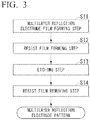
- a predetermined pattern is formed on the multilayer reflection electrode film 10 shown in FIG. 1 .
- a plurality of rectangular electrode units having one side length in a range of 10 ⁇ m to 500 ⁇ m are arranged on the substrate.
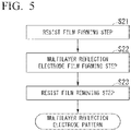
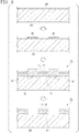
- the multilayer reflection electrode pattern 30 is formed as follows.
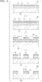
- the multilayer reflection electrode film 10 is formed on a film forming surface of the substrate 20 as a base material (multilayer reflection electrode film forming step S11).
- the underlayer oxide film 11 is formed as an underlayer on the substrate 20. It is preferable that the underlayer oxide film 11 is formed by DC sputtering using a sintered target with which the film composition can be easily controlled.
- the Ag film 12 is formed on the formed underlayer oxide film 11 by DC sputtering using an Ag target.
- the Ag target has a composition corresponding to the composition of the formed Ag film 12.
- the transparent conductive oxide film 13 is formed on the formed Ag film 12 by DC sputtering using a transparent conductive oxide target. It is preferable that the transparent conductive oxide target is a sintered target with which the film composition can be easily controlled. This way, the multilayer reflection electrode film 10 according to the embodiment is formed.
- a resist film 41 is formed on the multilayer reflection electrode film 10 formed on the surface of the substrate 20, and the resist film 41 is exposed and developed. As a result, a multilayer reflection electrode pattern is formed (resist film forming step S12).
- the multilayer reflection electrode film 10 on which the resist film 41 is formed is collectively etched by using an acidic mixed solution including phosphoric acid and acetic acid as an etchant (etching step S13).
- an acidic mixed solution including phosphoric acid and acetic acid it is preferable that the content of the phosphoric acid is 55 vol% or lower and the content of the acetic acid is 30 vol% or lower.
- the mixed solution may include 20 vol% or lower of nitric acid in addition to phosphoric acid and acetic acid.
- resist film removing step S14 the resist film 41 is removed using an alkaline resist remover.
- the multilayer reflection electrode film 10 positioned below the resist film 41 having a multilayer reflection electrode pattern shape remains, and the multilayer reflection electrode pattern 30 including the predetermined pattern is formed.
- the underlayer oxide film 11 is formed as an underlayer on the surface of the substrate 20, and the Ag film 12 is formed on the underlayer oxide film 11. Therefore, penetration of moisture or sulfur into the Ag film 12 can be suppressed, and deterioration of the Ag film 12 can be suppressed for a long period of time.
- Ga and one element or two or more elements selected from the group consisting of Sn, Y, and Ti are added to a Zn oxide, and atomic proportions with respect to all the metal elements included in each of the oxide films are Ga: 0.5 at% to 30.0 at%, each of Sn, Y, and Ti: 0.1 at% to 10.0 at%, and a balance of Zn. Therefore, due to the addition of Ga, adhesiveness between the Ag film 12 and the transparent conductive oxide film 13 can be improved, and an increase in electrical resistance can be suppressed. In addition, alkali resistance can be improved due to the addition of Sn, Y, and Ti. Further, the underlayer oxide film 11 and the transparent conductive oxide film 13 can suppress penetration of moisture or sulfur into the Ag film 12 to suppress deterioration of the Ag film 12.
- the Ag film 12 is formed of an Ag alloy including 0.2 at% to 2.0 at% of one element or two or more elements in total selected from the group consisting of Cu, In, Sn, Sb, Ti, Mg, Zn, Ge, Al, Ga, Pd, Au, Pt, Bi, Mn, Sc, Y, Nd, Sm, Eu, Gd, Tb, and Er and a balance of Ag and inevitable impurities. Therefore, sulfur resistance, heat resistance, or the like of the Ag film can be improved, and deterioration can be prevented. As a result, the Ag film 12 can be stably used for a long period of time.
- the multilayer reflection electrode pattern 30 has a high reflectance in a visible range, in particular, in a blue wavelength range, and a low resistance value.
- an organic EL display forms an image by combining blue light, green light, and red light emitted from an organic EL element that emits blue light, an organic EL element that emits green light, an organic EL element that emits red light, respectively. Therefore, in a case where the reflectance of the anode in a blue wavelength range is lower than that in a green wavelength range or red wavelength range, the emission amount of blue light increases, and thus it is necessary to increase the power input to the organic EL element that emits blue light. However, in a case where a large amount of power is input to the organic EL element that emits blue light, deterioration is likely to progress, and the emission amount of blue light decreases due to the deterioration of the organic EL element that emits blue light.
- the multilayer reflection electrode pattern 30 according to the embodiment has high reflectance with respect to light in a blue wavelength range. Therefore, it is not necessary to input a large amount of power to the organic EL element that emits blue light, and deterioration of the organic EL element is suppressed. As a result, a color balance of the organic EL display as a whole is stable for a long period of time.
- the acidic mixed solution including phosphoric acid and acetic acid is used as an etchant in the etching step S13, a difference in etching rate between the Ag film 12, the underlayer oxide film 11, and the transparent conductive oxide film 13 is small. Therefore, even in a case where the multilayer reflection electrode film 10 is collectively etched, the over-etching of the Ag film 12 or the remaining of residues of the underlayer oxide film 11 and the transparent conductive oxide film 13 can be prevented, and the multilayer reflection electrode pattern 30 can be accurately formed.
- alkali resistance of the transparent conductive oxide film 13 is improved due to the addition of one element or two or more elements selected from the group consisting of Sn, Y, and Ti. Therefore, even in a case where the resist film is removed using the alkaline resist remover in the resist film removing step S14, deterioration of the characteristics of the multilayer reflection electrode pattern can be prevented.
- the Ag film 12 is formed of an Ag alloy including 0.2 at% to 2.0 at% of one element or two or more elements in total selected from the group consisting of Cu, In, Sn, Sb, Ti, Mg, Zn, Ge, Al, Ga, Pd, Au, Pt, Bi, Mn, Sc, Y, Nd, Sm, Eu, Gd, Tb, and Er and a balance of Ag and inevitable impurities.
- the Ag film 12 is not limited to this configuration, and may be formed of pure Ag or an Ag alloy including another metal element that is solid-soluble in Ag.
- the underlayer oxide film 11 is formed of the same oxide as that forming the transparent conductive oxide film 13.
- the embodiment is not limited to this configuration.
- the underlayer oxide film 11 may be formed of ZnO or AZO. It is preferable that the underlayer oxide film 11 is formed of an oxide having a small difference in etching rate from the Ag film 12 and the transparent conductive oxide film 13.
- the underlayer oxide film 11 is disposed as an underlayer between the substrate 20 and the Ag film 12.
- the embodiment is not limited to this configuration, and the Ag film 12 may be directly disposed on the surface of the substrate 20.
- the multilayer reflection electrode pattern 30 is formed using an etching method.
- the embodiment is not limited to this configuration, and the multilayer reflection electrode pattern 30 may be formed using a lift-off method as shown in FIGS. 5 and 6 .
- the resist film 41 is formed on the film forming surface of the substrate 20, and the resist film 41 is exposed and developed. As a result, a reverse pattern having a reverse pattern shape of the multilayer reflection electrode pattern is formed (resist film forming step S21).
- the underlayer oxide film 11, the Ag film 12, and the transparent conductive oxide film 13 are sequentially formed using a sputtering method on the substrate 20 on which the resist film 41 including the reverse pattern is formed.
- the multilayer reflection electrode film 10 is formed on the resist film 41 and the substrate 20 (the multilayer reflection electrode film forming step S22).
- resist film removing step S23 the resist film 41 is removed using an alkaline resist remover.
- the multilayer reflection electrode film 10 formed on the resist film 41 having the reverse pattern shape is removed, and the multilayer reflection electrode pattern 30 including the predetermined pattern is formed.
- the predetermined pattern can be accurately formed without performing the etching step.
- alkali resistance of the transparent conductive oxide film 13 is improved due to the addition of one element or two or more elements selected from the group consisting of Sn, Y, and Ti. Therefore, even in a case where the resist film is removed using the alkaline resist remover in the resist film removing step S23, deterioration of the characteristics of the multilayer reflection electrode pattern 30 can be prevented.
- Each of multilayer reflection electrode films having structures shown in Tables 1 to 5 was formed on a surface of a glass substrate (non-alkali glass: 50 mm ⁇ 50 mm ⁇ 1 mmt) using a sputtering method.
- the thicknesses of the Ag film and the transparent conductive oxide films in each of Examples according to the present disclosure and Comparative Examples were measured using a film thickness meter (DEKTAK, manufactured by ULVAC Inc.).
- compositions of the transparent conductive oxide films and the Ag alloy film were obtained by performing elemental quantitative analysis using an ICP atomic emission spectrometer (STS-3500DD, manufactured by Hitachi High-Tech Science Corporation).
- oxide sintered body targets having compositions shown in Tables 1 to 5 were used.
- the composition of the ITO film (an oxide obtained by adding Sn to In 2 O3) shown in Table 5 was In: 35.6 at%, Sn: 3.6 at%, and O: 60.8 at%.
- multilayer reflection electrode films including a GZO film a composition of the film includes Zn: 47.3 at%, Ga: 2.2 at%, and O: 50.5 at%) instead of the ITO film in the compositions of Comparative Examples 1 to 5 were also prepared.
- Film forming conditions of each of the films are as follows.
- the evaluation methods are as follows.
- a reflectance spectrum in a wavelength range of 400 nm to 800 nm was measured to obtain an average reflectance in a blue wavelength range (400 to 500 nm) and an average reflectance in a visible range (400 to 800 nm).
- the measurement results are shown in Tables 6 to 10.
- a resist film was formed on the multilayer reflection electrode film using a photolithography method in an electrode pattern shape (line width/space width: 30 ⁇ m/30 ⁇ m).
- the multilayer transparent conductive film was collectively etched using a mixed solution (SEA-5, manufactured by Kanto Kagaku) including phosphoric acid and acetic acid as an etchant. Etching was performed for an appropriate etching time (20 seconds to 240 seconds) without heating.
- SEA-5 manufactured by Kanto Kagaku
- Etching was performed for an appropriate etching time (20 seconds to 240 seconds) without heating.
- the content of the phosphoric acid was 55 vol% or lower, and the content of the acetic acid was 30 vol%.
- the resist film was removed using an alkaline resist remover (pH9, TOK-104, manufactured by Tokyo Ohka Kogyo Co., Ltd.) to form an electrode pattern, and the formed electrode pattern was observed using an optical microscope (laser microscope VK-X200, manufactured by Keyence Corporation) at a magnification of 50 times to determine whether or not residues of the transparent conductive oxide film 13 were present. Specifically, in a case where the presence of the transparent conductive oxide film remaining in a needle shape or a particle shape without being etched was recognized, it was determined the residues of the transparent conductive oxide film 13 were present. Otherwise, it was determined that the residues of the transparent conductive oxide film 13 were not present.
- an alkaline resist remover pH9, TOK-104, manufactured by Tokyo Ohka Kogyo Co., Ltd.
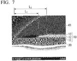
- FIG. 7 shows the result of observing a cross-sectional shape of the electrode pattern obtained in the patterning test in which thee multilayer reflection electrode film formed in Example 2 was used. As shown in FIG.
- the length L 1 is the length between an end portion of the resist film 41 and an end portion of the Ag film 12 in a direction parallel to the film forming surface of the substrate 20.
- the length L 2 is the length between an end portion of the resist film 41 and an end portion of the transparent conductive oxide film 13 in the direction parallel to the film forming surface of the substrate 20.
- a resist solution was applied to the substrate, a photomask on which an electrode pattern (line width/space width: 30 ⁇ m/30 ⁇ m) was formed was attached thereto, and the substrate was exposed to ultraviolet light using an exposure machine. Next, the exposed portion was removed using a developer, and a reverse pattern was formed using a photolithography method.
- the multilayer reflection electrode film was formed using the sputtering device as described above on the substrate on which the reverse pattern was formed.
- the substrate was dipped in a resist remover (ph9, TOK-104, manufactured by Tokyo Ohka Kogyo Co., Ltd.) to remove the multilayer reflection electrode film formed on the resist film, and then the formed electrode pattern was observed using an optical microscope (laser microscope VK-X200, manufactured by Keyence Corporation) at a magnification of 50 times to measure the accuracy of the electrode pattern.
- a resist remover ph9, TOK-104, manufactured by Tokyo Ohka Kogyo Co., Ltd.
- the average reflectance in a blue wavelength range was 86% or higher and the average reflectance in the visible range was 95% or higher, and the sheet resistance after film formation was 0.5 ⁇ /sq. or lower except for the samples (Examples 52 and 70) in which the thickness of the Ag film was 50 nm. Therefore, it was found that the multilayer film having high reflectance and sufficiently low resistance was obtained. In Examples 52 and 70, the thickness of the Ag film was thin at 50 nm. Therefore, the sheet resistance was about 0.8 ⁇ /sq., and the reflectance was slightly low.
- the thickness of the transparent conductive oxide film formed on the Ag film was thick at 100 nm, and the absorptance increased. Therefore, the reflectance was slightly lower than that of the sample having a thickness of 10 nm.
- the average reflectance in the blue wavelength range were lower than 86% and the average reflectance in a visible range were lower than 95%, which were lower than those of Examples.
- the results of the patterning test using the etching method are as follows.
- the length of over-etching of the multilayer film was 1 ⁇ m or less, and thus it was found that an electrode pattern having no residues of the transparent conductive oxide film can be accurately formed.
- the results of observing the surface of electrode pattern by visual inspection after the removal of the resist are as follows. In Examples, a change of the surface was not observed as compared to that before the test. On the other hand, in the multilayer films according to Comparative Examples in which the GZO film not including Sn, Y, and Ti was formed as the transparent conductive oxide film, film peeling was observed in places after the removal of the resist.
- the reflectance in the visible range, in particular, in the blue wavelength range is high, and the resistance value is low.
- a fine electrode pattern can be easily formed using an etching method. Therefore, the multilayer reflection electrode film can be suitably used as, for example, an anode of an organic electroluminescence (EL) element.
- EL organic electroluminescence
Landscapes
- Engineering & Computer Science (AREA)
- Manufacturing & Machinery (AREA)
- Physics & Mathematics (AREA)
- Optics & Photonics (AREA)
- Electroluminescent Light Sources (AREA)
- Laminated Bodies (AREA)
Applications Claiming Priority (3)
| Application Number | Priority Date | Filing Date | Title |
|---|---|---|---|
| JP2016059097 | 2016-03-23 | ||
| JP2017024269A JP6776931B2 (ja) | 2016-03-23 | 2017-02-13 | 積層反射電極膜、積層反射電極パターン、積層反射電極パターンの製造方法 |
| PCT/JP2017/011347 WO2017164211A1 (ja) | 2016-03-23 | 2017-03-22 | 積層反射電極膜、積層反射電極パターン、積層反射電極パターンの製造方法 |
Publications (3)
| Publication Number | Publication Date |
|---|---|
| EP3435741A1 true EP3435741A1 (de) | 2019-01-30 |
| EP3435741A4 EP3435741A4 (de) | 2019-12-04 |
| EP3435741B1 EP3435741B1 (de) | 2021-09-08 |
Family
ID=60007631
Family Applications (1)
| Application Number | Title | Priority Date | Filing Date |
|---|---|---|---|
| EP17770251.1A Not-in-force EP3435741B1 (de) | 2016-03-23 | 2017-03-22 | Laminierte reflektierende elektrodenfolie, laminiertes reflektierendes elektrodenmuster und verfahren zur herstellung des laminierten reflektierenden elektrodenmusters |
Country Status (6)
| Country | Link |
|---|---|
| US (1) | US10971695B2 (de) |
| EP (1) | EP3435741B1 (de) |
| JP (1) | JP6776931B2 (de) |
| KR (1) | KR102327961B1 (de) |
| CN (1) | CN108886857B (de) |
| TW (1) | TWI722146B (de) |
Families Citing this family (10)
| Publication number | Priority date | Publication date | Assignee | Title |
|---|---|---|---|---|
| JP6888318B2 (ja) * | 2016-03-23 | 2021-06-16 | 三菱マテリアル株式会社 | 積層透明導電膜、積層配線膜及び積層配線膜の製造方法 |
| CN109524575A (zh) * | 2018-12-05 | 2019-03-26 | 武汉华星光电半导体显示技术有限公司 | Oled显示面板的制作方法及oled显示面板 |
| JP2020090706A (ja) | 2018-12-05 | 2020-06-11 | 三菱マテリアル株式会社 | 金属膜、及び、スパッタリングターゲット |
| JP2020090708A (ja) | 2018-12-05 | 2020-06-11 | 三菱マテリアル株式会社 | 金属膜、及び、スパッタリングターゲット |
| JP2020090707A (ja) | 2018-12-05 | 2020-06-11 | 三菱マテリアル株式会社 | 金属膜、及び、スパッタリングターゲット |
| WO2021176506A1 (ja) * | 2020-03-02 | 2021-09-10 | シャープ株式会社 | 表示装置およびその製造方法 |
| EP3958291A1 (de) * | 2020-08-21 | 2022-02-23 | Ams Ag | Verfahren zur herstellung einer abhebemaskenstruktur |
| CN113054142B (zh) * | 2021-04-02 | 2023-01-31 | 深圳市芯视佳半导体科技有限公司 | 一种硅基oled微显示器阳极及其制备方法和应用 |
| CN117970687A (zh) * | 2022-10-26 | 2024-05-03 | 瀚宇彩晶股份有限公司 | 显示面板 |
| CN118057597A (zh) * | 2022-11-18 | 2024-05-21 | 瀚宇彩晶股份有限公司 | 蚀刻液和显示面板的制作方法 |
Family Cites Families (24)
| Publication number | Priority date | Publication date | Assignee | Title |
|---|---|---|---|---|
| JPH1040740A (ja) * | 1996-07-26 | 1998-02-13 | Kojundo Chem Lab Co Ltd | 透明導電膜および透明導電材料 |
| JP2000133466A (ja) | 1998-10-23 | 2000-05-12 | Canon Inc | 表面改質ito膜、その表面処理方法およびそれを用いた電荷注入型発光素子 |
| US6559594B2 (en) | 2000-02-03 | 2003-05-06 | Semiconductor Energy Laboratory Co., Ltd. | Light-emitting device |
| JP2002363732A (ja) | 2001-03-15 | 2002-12-18 | Asahi Glass Co Ltd | 透明導電膜の製造方法および透明導電膜付き透明基板 |
| JP4186101B2 (ja) | 2002-09-04 | 2008-11-26 | ソニー株式会社 | 有機el表示装置 |
| JP2004156070A (ja) * | 2002-11-01 | 2004-06-03 | Kanto Chem Co Inc | 透明導電膜を含む積層膜のエッチング液組成物 |
| JP2006098856A (ja) | 2004-09-30 | 2006-04-13 | Ulvac Japan Ltd | Ag系反射膜およびその作製方法 |
| JP2006294261A (ja) | 2005-04-05 | 2006-10-26 | Fuji Electric Holdings Co Ltd | 有機el発光素子およびその製造方法 |
| KR101241524B1 (ko) * | 2005-09-01 | 2013-03-11 | 이데미쓰 고산 가부시키가이샤 | 스퍼터링 타겟, 투명 도전막 및 투명 전극 |
| FR2924274B1 (fr) | 2007-11-22 | 2012-11-30 | Saint Gobain | Substrat porteur d'une electrode, dispositif electroluminescent organique l'incorporant, et sa fabrication |
| JP5003600B2 (ja) | 2008-06-13 | 2012-08-15 | 住友金属鉱山株式会社 | 酸化物焼結体、ターゲット、およびそれを用いて得られる透明導電膜、導電性積層体 |
| JP4295811B1 (ja) | 2008-09-17 | 2009-07-15 | 三井金属鉱業株式会社 | 酸化亜鉛系ターゲット |
| JP4723692B2 (ja) | 2008-09-19 | 2011-07-13 | パナソニック株式会社 | 有機エレクトロルミネッセンス素子及びその製造方法 |
| KR101422362B1 (ko) * | 2009-07-10 | 2014-07-22 | 가부시키가이샤 한도오따이 에네루기 켄큐쇼 | 표시 장치, 표시 패널 및 전자 기기 |
| KR101047652B1 (ko) * | 2009-12-18 | 2011-07-07 | 엘지이노텍 주식회사 | 발광소자 및 그 제조방법 |
| KR20120123185A (ko) * | 2011-04-19 | 2012-11-08 | 삼성디스플레이 주식회사 | 유기 전계 발광 표시 장치 |
| JP2012246511A (ja) | 2011-05-25 | 2012-12-13 | Geomatec Co Ltd | 金属薄膜積層基板の製造方法及び静電容量型タッチパネルの製造方法 |
| KR20130000218A (ko) * | 2011-06-22 | 2013-01-02 | 삼성디스플레이 주식회사 | 자성체 물질을 함유한 전극 및 상기 전극을 갖는 유기발광소자 |
| JP2013105546A (ja) | 2011-11-10 | 2013-05-30 | Ulvac Japan Ltd | 有機el表示装置、led装置、太陽電池、反射膜 |
| US9419174B2 (en) * | 2012-09-26 | 2016-08-16 | University Of Florida Research Foundation, Inc. | Transparent quantum dot light-emitting diodes with dielectric/metal/dielectric electrode |
| JP6375658B2 (ja) * | 2014-03-19 | 2018-08-22 | 三菱マテリアル株式会社 | 積層膜 |
| JP2016040411A (ja) * | 2014-08-12 | 2016-03-24 | 三菱マテリアル株式会社 | 積層膜、積層配線膜及び積層配線膜の製造方法 |
| CN106575090B (zh) * | 2014-08-25 | 2020-02-07 | 日产化学工业株式会社 | 用于soc图案上的图案反转的被覆用组合物 |
| WO2016063169A1 (en) | 2014-10-23 | 2016-04-28 | Semiconductor Energy Laboratory Co., Ltd. | Light-emitting element |
-
2017
- 2017-02-13 JP JP2017024269A patent/JP6776931B2/ja not_active Expired - Fee Related
- 2017-03-22 KR KR1020187025183A patent/KR102327961B1/ko not_active Expired - Fee Related
- 2017-03-22 CN CN201780018466.6A patent/CN108886857B/zh not_active Expired - Fee Related
- 2017-03-22 US US16/086,623 patent/US10971695B2/en not_active Expired - Fee Related
- 2017-03-22 TW TW106109573A patent/TWI722146B/zh not_active IP Right Cessation
- 2017-03-22 EP EP17770251.1A patent/EP3435741B1/de not_active Not-in-force
Also Published As
| Publication number | Publication date |
|---|---|
| EP3435741A4 (de) | 2019-12-04 |
| CN108886857B (zh) | 2021-04-02 |
| KR20180124855A (ko) | 2018-11-21 |
| CN108886857A (zh) | 2018-11-23 |
| TWI722146B (zh) | 2021-03-21 |
| EP3435741B1 (de) | 2021-09-08 |
| JP6776931B2 (ja) | 2020-10-28 |
| KR102327961B1 (ko) | 2021-11-17 |
| US10971695B2 (en) | 2021-04-06 |
| TW201803409A (zh) | 2018-01-16 |
| US20190103580A1 (en) | 2019-04-04 |
| JP2017183274A (ja) | 2017-10-05 |
Similar Documents
| Publication | Publication Date | Title |
|---|---|---|
| EP3435741B1 (de) | Laminierte reflektierende elektrodenfolie, laminiertes reflektierendes elektrodenmuster und verfahren zur herstellung des laminierten reflektierenden elektrodenmusters | |
| EP3435385B1 (de) | Laminierte transparente leitfähige folie, laminierte verdrahtungsfolie und verfahren zur herstellung einer laminierten verdrahtungsfolie | |
| JP5235011B2 (ja) | 有機elディスプレイ用の反射アノード電極 | |
| KR101745290B1 (ko) | 반사 전극용 Ag 합금막 및 반사 전극 | |
| JP2010161185A (ja) | 有機el表示装置、有機el表示装置の製造方法 | |
| JP2004158442A (ja) | 積層体、配線付き基体、有機el表示素子、有機el表示素子の接続端子及びそれらの製造方法 | |
| JP6962376B2 (ja) | 透明導電体及び有機デバイス | |
| JP6870332B2 (ja) | 積層透明導電膜、積層配線膜及び積層配線膜の製造方法 | |
| WO2017164211A1 (ja) | 積層反射電極膜、積層反射電極パターン、積層反射電極パターンの製造方法 | |
| KR102198608B1 (ko) | 은 박막 식각액 조성물 및 이를 이용한 식각 방법 및 금속 패턴의 형성 방법 | |
| WO2006132412A1 (ja) | 電極、配線及び電磁波遮蔽用の銀合金 | |
| WO2014041974A1 (ja) | 有機EL素子のアノード電極用Al合金膜、有機EL素子およびAl合金スパッタリングターゲット | |
| KR102623991B1 (ko) | 은 함유 박막 식각액 조성물 및 이를 이용하여 제조된 표시장치용 어레이기판 및 이의 제조방법 | |
| JP6384147B2 (ja) | 半透明Ag合金膜 | |
| KR20210000301A (ko) | 은 박막 식각액 조성물 및 이를 이용한 식각 방법 및 금속 패턴의 형성 방법 | |
| JPWO2005031681A1 (ja) | 配線付き基体形成用積層体、配線付き基体およびそれらの製造方法 | |
| WO2014038560A1 (ja) | 有機EL素子、有機EL素子の反射電極の製造方法、および有機EL素子の反射電極形成用Al合金スパッタリングターゲット | |
| JP2008235004A (ja) | ZnS系透明導電性薄膜、ZnS系透明導電性蛍光体薄膜、および、この薄膜の成膜用のスパッタリングターゲット材料 | |
| TW202109934A (zh) | 層合膜 | |
| WO2014020789A1 (ja) | 有機電界発光素子および有機電界発光素子の製造方法 |
Legal Events
| Date | Code | Title | Description |
|---|---|---|---|
| STAA | Information on the status of an ep patent application or granted ep patent |
Free format text: STATUS: THE INTERNATIONAL PUBLICATION HAS BEEN MADE |
|
| PUAI | Public reference made under article 153(3) epc to a published international application that has entered the european phase |
Free format text: ORIGINAL CODE: 0009012 |
|
| STAA | Information on the status of an ep patent application or granted ep patent |
Free format text: STATUS: REQUEST FOR EXAMINATION WAS MADE |
|
| 17P | Request for examination filed |
Effective date: 20180925 |
|
| AK | Designated contracting states |
Kind code of ref document: A1 Designated state(s): AL AT BE BG CH CY CZ DE DK EE ES FI FR GB GR HR HU IE IS IT LI LT LU LV MC MK MT NL NO PL PT RO RS SE SI SK SM TR |
|
| AX | Request for extension of the european patent |
Extension state: BA ME |
|
| DAV | Request for validation of the european patent (deleted) | ||
| DAX | Request for extension of the european patent (deleted) | ||
| RAP1 | Party data changed (applicant data changed or rights of an application transferred) |
Owner name: MITSUBISHI MATERIALS CORPORATION |
|
| A4 | Supplementary search report drawn up and despatched |
Effective date: 20191106 |
|
| RIC1 | Information provided on ipc code assigned before grant |
Ipc: H05B 33/10 20060101ALI20191030BHEP Ipc: H05B 33/26 20060101AFI20191030BHEP Ipc: H01L 51/50 20060101ALI20191030BHEP Ipc: H01B 1/02 20060101ALI20191030BHEP Ipc: H01L 51/52 20060101ALI20191030BHEP |
|
| STAA | Information on the status of an ep patent application or granted ep patent |
Free format text: STATUS: EXAMINATION IS IN PROGRESS |
|
| 17Q | First examination report despatched |
Effective date: 20201020 |
|
| GRAP | Despatch of communication of intention to grant a patent |
Free format text: ORIGINAL CODE: EPIDOSNIGR1 |
|
| STAA | Information on the status of an ep patent application or granted ep patent |
Free format text: STATUS: GRANT OF PATENT IS INTENDED |
|
| INTG | Intention to grant announced |
Effective date: 20210423 |
|
| GRAS | Grant fee paid |
Free format text: ORIGINAL CODE: EPIDOSNIGR3 |
|
| GRAA | (expected) grant |
Free format text: ORIGINAL CODE: 0009210 |
|
| STAA | Information on the status of an ep patent application or granted ep patent |
Free format text: STATUS: THE PATENT HAS BEEN GRANTED |
|
| AK | Designated contracting states |
Kind code of ref document: B1 Designated state(s): AL AT BE BG CH CY CZ DE DK EE ES FI FR GB GR HR HU IE IS IT LI LT LU LV MC MK MT NL NO PL PT RO RS SE SI SK SM TR |
|
| REG | Reference to a national code |
Ref country code: GB Ref legal event code: FG4D |
|
| REG | Reference to a national code |
Ref country code: AT Ref legal event code: REF Ref document number: 1429758 Country of ref document: AT Kind code of ref document: T Effective date: 20210915 Ref country code: CH Ref legal event code: EP |
|
| REG | Reference to a national code |
Ref country code: IE Ref legal event code: FG4D |
|
| REG | Reference to a national code |
Ref country code: DE Ref legal event code: R096 Ref document number: 602017045711 Country of ref document: DE |
|
| REG | Reference to a national code |
Ref country code: LT Ref legal event code: MG9D |
|
| REG | Reference to a national code |
Ref country code: NL Ref legal event code: MP Effective date: 20210908 |
|
| PG25 | Lapsed in a contracting state [announced via postgrant information from national office to epo] |
Ref country code: HR Free format text: LAPSE BECAUSE OF FAILURE TO SUBMIT A TRANSLATION OF THE DESCRIPTION OR TO PAY THE FEE WITHIN THE PRESCRIBED TIME-LIMIT Effective date: 20210908 Ref country code: RS Free format text: LAPSE BECAUSE OF FAILURE TO SUBMIT A TRANSLATION OF THE DESCRIPTION OR TO PAY THE FEE WITHIN THE PRESCRIBED TIME-LIMIT Effective date: 20210908 Ref country code: SE Free format text: LAPSE BECAUSE OF FAILURE TO SUBMIT A TRANSLATION OF THE DESCRIPTION OR TO PAY THE FEE WITHIN THE PRESCRIBED TIME-LIMIT Effective date: 20210908 Ref country code: LT Free format text: LAPSE BECAUSE OF FAILURE TO SUBMIT A TRANSLATION OF THE DESCRIPTION OR TO PAY THE FEE WITHIN THE PRESCRIBED TIME-LIMIT Effective date: 20210908 Ref country code: BG Free format text: LAPSE BECAUSE OF FAILURE TO SUBMIT A TRANSLATION OF THE DESCRIPTION OR TO PAY THE FEE WITHIN THE PRESCRIBED TIME-LIMIT Effective date: 20211208 Ref country code: ES Free format text: LAPSE BECAUSE OF FAILURE TO SUBMIT A TRANSLATION OF THE DESCRIPTION OR TO PAY THE FEE WITHIN THE PRESCRIBED TIME-LIMIT Effective date: 20210908 Ref country code: FI Free format text: LAPSE BECAUSE OF FAILURE TO SUBMIT A TRANSLATION OF THE DESCRIPTION OR TO PAY THE FEE WITHIN THE PRESCRIBED TIME-LIMIT Effective date: 20210908 Ref country code: NO Free format text: LAPSE BECAUSE OF FAILURE TO SUBMIT A TRANSLATION OF THE DESCRIPTION OR TO PAY THE FEE WITHIN THE PRESCRIBED TIME-LIMIT Effective date: 20211208 |
|
| REG | Reference to a national code |
Ref country code: AT Ref legal event code: MK05 Ref document number: 1429758 Country of ref document: AT Kind code of ref document: T Effective date: 20210908 |
|
| PG25 | Lapsed in a contracting state [announced via postgrant information from national office to epo] |
Ref country code: LV Free format text: LAPSE BECAUSE OF FAILURE TO SUBMIT A TRANSLATION OF THE DESCRIPTION OR TO PAY THE FEE WITHIN THE PRESCRIBED TIME-LIMIT Effective date: 20210908 Ref country code: GR Free format text: LAPSE BECAUSE OF FAILURE TO SUBMIT A TRANSLATION OF THE DESCRIPTION OR TO PAY THE FEE WITHIN THE PRESCRIBED TIME-LIMIT Effective date: 20211209 |
|
| PG25 | Lapsed in a contracting state [announced via postgrant information from national office to epo] |
Ref country code: AT Free format text: LAPSE BECAUSE OF FAILURE TO SUBMIT A TRANSLATION OF THE DESCRIPTION OR TO PAY THE FEE WITHIN THE PRESCRIBED TIME-LIMIT Effective date: 20210908 |
|
| PGFP | Annual fee paid to national office [announced via postgrant information from national office to epo] |
Ref country code: DE Payment date: 20220314 Year of fee payment: 6 |
|
| PG25 | Lapsed in a contracting state [announced via postgrant information from national office to epo] |
Ref country code: IS Free format text: LAPSE BECAUSE OF FAILURE TO SUBMIT A TRANSLATION OF THE DESCRIPTION OR TO PAY THE FEE WITHIN THE PRESCRIBED TIME-LIMIT Effective date: 20220108 Ref country code: SM Free format text: LAPSE BECAUSE OF FAILURE TO SUBMIT A TRANSLATION OF THE DESCRIPTION OR TO PAY THE FEE WITHIN THE PRESCRIBED TIME-LIMIT Effective date: 20210908 Ref country code: SK Free format text: LAPSE BECAUSE OF FAILURE TO SUBMIT A TRANSLATION OF THE DESCRIPTION OR TO PAY THE FEE WITHIN THE PRESCRIBED TIME-LIMIT Effective date: 20210908 Ref country code: RO Free format text: LAPSE BECAUSE OF FAILURE TO SUBMIT A TRANSLATION OF THE DESCRIPTION OR TO PAY THE FEE WITHIN THE PRESCRIBED TIME-LIMIT Effective date: 20210908 Ref country code: PT Free format text: LAPSE BECAUSE OF FAILURE TO SUBMIT A TRANSLATION OF THE DESCRIPTION OR TO PAY THE FEE WITHIN THE PRESCRIBED TIME-LIMIT Effective date: 20220110 Ref country code: PL Free format text: LAPSE BECAUSE OF FAILURE TO SUBMIT A TRANSLATION OF THE DESCRIPTION OR TO PAY THE FEE WITHIN THE PRESCRIBED TIME-LIMIT Effective date: 20210908 Ref country code: NL Free format text: LAPSE BECAUSE OF FAILURE TO SUBMIT A TRANSLATION OF THE DESCRIPTION OR TO PAY THE FEE WITHIN THE PRESCRIBED TIME-LIMIT Effective date: 20210908 Ref country code: EE Free format text: LAPSE BECAUSE OF FAILURE TO SUBMIT A TRANSLATION OF THE DESCRIPTION OR TO PAY THE FEE WITHIN THE PRESCRIBED TIME-LIMIT Effective date: 20210908 Ref country code: CZ Free format text: LAPSE BECAUSE OF FAILURE TO SUBMIT A TRANSLATION OF THE DESCRIPTION OR TO PAY THE FEE WITHIN THE PRESCRIBED TIME-LIMIT Effective date: 20210908 Ref country code: AL Free format text: LAPSE BECAUSE OF FAILURE TO SUBMIT A TRANSLATION OF THE DESCRIPTION OR TO PAY THE FEE WITHIN THE PRESCRIBED TIME-LIMIT Effective date: 20210908 |
|
| REG | Reference to a national code |
Ref country code: DE Ref legal event code: R097 Ref document number: 602017045711 Country of ref document: DE |
|
| PLBE | No opposition filed within time limit |
Free format text: ORIGINAL CODE: 0009261 |
|
| STAA | Information on the status of an ep patent application or granted ep patent |
Free format text: STATUS: NO OPPOSITION FILED WITHIN TIME LIMIT |
|
| PG25 | Lapsed in a contracting state [announced via postgrant information from national office to epo] |
Ref country code: DK Free format text: LAPSE BECAUSE OF FAILURE TO SUBMIT A TRANSLATION OF THE DESCRIPTION OR TO PAY THE FEE WITHIN THE PRESCRIBED TIME-LIMIT Effective date: 20210908 |
|
| 26N | No opposition filed |
Effective date: 20220609 |
|
| PG25 | Lapsed in a contracting state [announced via postgrant information from national office to epo] |
Ref country code: SI Free format text: LAPSE BECAUSE OF FAILURE TO SUBMIT A TRANSLATION OF THE DESCRIPTION OR TO PAY THE FEE WITHIN THE PRESCRIBED TIME-LIMIT Effective date: 20210908 |
|
| PG25 | Lapsed in a contracting state [announced via postgrant information from national office to epo] |
Ref country code: MC Free format text: LAPSE BECAUSE OF FAILURE TO SUBMIT A TRANSLATION OF THE DESCRIPTION OR TO PAY THE FEE WITHIN THE PRESCRIBED TIME-LIMIT Effective date: 20210908 |
|
| REG | Reference to a national code |
Ref country code: CH Ref legal event code: PL |
|
| GBPC | Gb: european patent ceased through non-payment of renewal fee |
Effective date: 20220322 |
|
| REG | Reference to a national code |
Ref country code: BE Ref legal event code: MM Effective date: 20220331 |
|
| PG25 | Lapsed in a contracting state [announced via postgrant information from national office to epo] |
Ref country code: LU Free format text: LAPSE BECAUSE OF NON-PAYMENT OF DUE FEES Effective date: 20220322 Ref country code: LI Free format text: LAPSE BECAUSE OF NON-PAYMENT OF DUE FEES Effective date: 20220331 Ref country code: IT Free format text: LAPSE BECAUSE OF FAILURE TO SUBMIT A TRANSLATION OF THE DESCRIPTION OR TO PAY THE FEE WITHIN THE PRESCRIBED TIME-LIMIT Effective date: 20210908 Ref country code: IE Free format text: LAPSE BECAUSE OF NON-PAYMENT OF DUE FEES Effective date: 20220322 Ref country code: GB Free format text: LAPSE BECAUSE OF NON-PAYMENT OF DUE FEES Effective date: 20220322 Ref country code: FR Free format text: LAPSE BECAUSE OF NON-PAYMENT OF DUE FEES Effective date: 20220331 Ref country code: CH Free format text: LAPSE BECAUSE OF NON-PAYMENT OF DUE FEES Effective date: 20220331 |
|
| PG25 | Lapsed in a contracting state [announced via postgrant information from national office to epo] |
Ref country code: BE Free format text: LAPSE BECAUSE OF NON-PAYMENT OF DUE FEES Effective date: 20220331 |
|
| REG | Reference to a national code |
Ref country code: DE Ref legal event code: R119 Ref document number: 602017045711 Country of ref document: DE |
|
| PG25 | Lapsed in a contracting state [announced via postgrant information from national office to epo] |
Ref country code: DE Free format text: LAPSE BECAUSE OF NON-PAYMENT OF DUE FEES Effective date: 20231003 |
|
| PG25 | Lapsed in a contracting state [announced via postgrant information from national office to epo] |
Ref country code: HU Free format text: LAPSE BECAUSE OF FAILURE TO SUBMIT A TRANSLATION OF THE DESCRIPTION OR TO PAY THE FEE WITHIN THE PRESCRIBED TIME-LIMIT; INVALID AB INITIO Effective date: 20170322 |
|
| PG25 | Lapsed in a contracting state [announced via postgrant information from national office to epo] |
Ref country code: MK Free format text: LAPSE BECAUSE OF FAILURE TO SUBMIT A TRANSLATION OF THE DESCRIPTION OR TO PAY THE FEE WITHIN THE PRESCRIBED TIME-LIMIT Effective date: 20210908 Ref country code: CY Free format text: LAPSE BECAUSE OF FAILURE TO SUBMIT A TRANSLATION OF THE DESCRIPTION OR TO PAY THE FEE WITHIN THE PRESCRIBED TIME-LIMIT Effective date: 20210908 |
|
| PG25 | Lapsed in a contracting state [announced via postgrant information from national office to epo] |
Ref country code: MT Free format text: LAPSE BECAUSE OF FAILURE TO SUBMIT A TRANSLATION OF THE DESCRIPTION OR TO PAY THE FEE WITHIN THE PRESCRIBED TIME-LIMIT Effective date: 20210908 |
|
| PG25 | Lapsed in a contracting state [announced via postgrant information from national office to epo] |
Ref country code: TR Free format text: LAPSE BECAUSE OF FAILURE TO SUBMIT A TRANSLATION OF THE DESCRIPTION OR TO PAY THE FEE WITHIN THE PRESCRIBED TIME-LIMIT Effective date: 20210908 |