EP3438677B1 - Verfahren zur bestimmung eines elektrischen parameters und messanordnung zur bestimmung eines elektrischen parameters - Google Patents
Verfahren zur bestimmung eines elektrischen parameters und messanordnung zur bestimmung eines elektrischen parameters Download PDFInfo
- Publication number
- EP3438677B1 EP3438677B1 EP17184021.8A EP17184021A EP3438677B1 EP 3438677 B1 EP3438677 B1 EP 3438677B1 EP 17184021 A EP17184021 A EP 17184021A EP 3438677 B1 EP3438677 B1 EP 3438677B1
- Authority
- EP
- European Patent Office
- Prior art keywords
- capacitor
- discharging
- time
- voltage
- measurement
- Prior art date
- Legal status (The legal status is an assumption and is not a legal conclusion. Google has not performed a legal analysis and makes no representation as to the accuracy of the status listed.)
- Active
Links
Images

Classifications
-
- G—PHYSICS
- G01—MEASURING; TESTING
- G01R—MEASURING ELECTRIC VARIABLES; MEASURING MAGNETIC VARIABLES
- G01R27/00—Arrangements for measuring resistance, reactance, impedance, or electric characteristics derived therefrom
- G01R27/02—Measuring real or complex resistance, reactance, impedance, or other two-pole characteristics derived therefrom, e.g. time constant
- G01R27/26—Measuring inductance or capacitance; Measuring quality factor, e.g. by using the resonance method; Measuring loss factor; Measuring dielectric constants ; Measuring impedance or related variables
- G01R27/2605—Measuring capacitance
-
- G—PHYSICS
- G01—MEASURING; TESTING
- G01R—MEASURING ELECTRIC VARIABLES; MEASURING MAGNETIC VARIABLES
- G01R27/00—Arrangements for measuring resistance, reactance, impedance, or electric characteristics derived therefrom
- G01R27/02—Measuring real or complex resistance, reactance, impedance, or other two-pole characteristics derived therefrom, e.g. time constant
Definitions
- the proposed concept allows for employing a similar or equal starting voltage at the measurement of the first discharge time and at the measurement of the second discharge time.
- the starting voltages may be represented by the common supply voltage and have a similar or same level of noise which tends to cancel out in the ratio calculation of the electrical parameter.
- fewer or even no noise is introduced to the measurement by the common supply voltage as power supply.
- the effect of the power supply voltage noise on the measurements can be reduced or eliminated completely.
- a higher power supply noise can be tolerated. This allows for increased measurement accuracy without increasing the amount of external components.
- the discharging of the first capacitor comprises further steps.
- the discharging is started and stopped when the first voltage reaches a threshold voltage.
- the first discharge time denotes a time between start and stop of discharging the first capacitor.
- discharging the second capacitor is started and stopped when the second of voltage reaches the threshold voltage.
- the second discharge time then denotes a time between start and stop of discharging the second capacitor.
- the first capacitor and the second capacitor are charged simultaneously.
- the parallel charging of the first and the second capacitor starts at a same instant in time, e.g. are synchronized to each other.
- the first capacitor has a first capacitance value.
- the second capacitor has a second capacitance value.
- the capacitance values may be close in value to each other, e.g. the capacitance values are the same with process parameters or may differ only by values smaller than 10% or smaller than 1%.
- the first and second capacitance value can be proportional in value to each other. In some embodiments the first and second capacitance value can be matched or even be same in value.
- the first capacitor is charged with the common supply voltage using the second capacitor.
- the capacitor is charged before the first capacitor is discharged for a second time.
- the second capacitor is used to recharge the first capacitor with the common supply voltage. Then the first capacitor can be discharged to yield the second (or further) discharge time.
- further capacitors are charged from the common supply voltage in parallel with the first and the second capacitors. Further discharge times are determined by discharging the further capacitors, respectively. Further electrical parameters are then determined from ratios of the first, the second and the further discharge times, respectively.
- the same concepts described herein with respect to the first and the second capacitor may be applied also to the further capacitors.
- the electrical parameter to be determined may be formulated as a function of several capacitance and/or resistance values.
- At least one electrical parameter to be determined is a resistance ratio and/or a capacitance ratio.
- the resistance ratio and/or a capacitance ratio is indicative of a measurement object such as a sensor which may be connected to a measurement arrangement, e.g. by means of terminals and switches, wherein the measurement arrangement implements the method for determining the electrical parameter as disclosed herein.
- a measurement arrangement for determining an electrical parameter comprises a measurement path and a data analysis path.
- the measurement path is arranged to be connected to a first and a second capacitor, respectively.
- the measurement path is further arranged to provide a common supply voltage.
- the data analysis path is connected to the measurement path and configured to determine the electrical parameter according to the method for determining the electrical parameter as discussed above.
- the data analysis path further comprises a comparator, a time-to-digital converter and a control and processing unit, which are connected in series.
- the comparator is arranged to provide a trigger signal when a voltage applied at an input side reaches a threshold voltage.
- the comparator is connected to the measurement path.
- the time-to-digital converter is arranged to provide a timing signal depending on the trigger signal.
- control and processing unit is arranged to select the first and the second selectable terminal in order to charge, in parallel, the first and the second capacitor from the common supply voltage provided at the load supply terminal. Furthermore, the control and processing unit is also arranged to select the first and the second selectable terminal to discharge the first and/or the second capacitor, respectively.
- the measurement arrangement comprises an integrated circuit.
- the first and second capacitor and/or the at least one resistor or integrated into the same integrated circuit or, alternatively, are connected to the selectable terminals as external components, respectively.
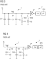
- Figure 1 shows a method and measurement arrangement for determining a resistance ratio.
- the measurement arrangement comprises a measurement path 1 and a data analysis path 2.
- the measurement arrangement can be implemented as an integrated circuit with the measurement path 1 and the data analysis path 2 integrated into the same integrated circuit, e.g. a common die or package.
- the measurement arrangement comprises selectable input terminals to connect a strain gauge SG or a capacitive sensor to be measured.
- the time-to-digital converter TDC is connected to an output of the comparator, and, further, to connected to the control and processing unit CPU.
- the time-to-digital converter TDC is adapted to recognize events, such as a start and a stop of discharging a capacitor, and to provide a digital output signal which is a representation of the respective instances in time.
- the time-to-digital converter TDC might output a start signal indicating the start of discharging a capacitor.
- a stop signal might be output indicating the stop of discharging a capacitor.
- a discharge time could then be derived from a digital difference of the start and stop signals.
- the discharge time can be measured directly as a time interval between start and stop instances of discharging rather than as an absolute time difference.
- a first measurement sequence can be used to determine a ratio of resistance values.
- the first measurement sequence involves the following procedural steps.
- step s1-2 the first capacitor CL1 is discharged through the first resistor R1.
- Switches S1 and S3 are open while switch S2 remains closed.
- Discharging the first capacitor CL1 by means of the first resistor R1 is started by closing switch S4 while S5 remains open.
- the time-to-digital converter TDC is triggered to start a measurement of a first discharge time t11.
- the start can be triggered by the control and processing unit CPU or by detecting the voltage VL1 stored on the first capacitor CL1 to drop, e.g. measured by means of the comparator CP.
- the comparator CP switches when the voltage VL1 drops below a threshold voltage Vth.
- a trigger signal Sout which is provided by the comparator CP when the voltage applied at its input side reaches the threshold voltage Vth.
- the trigger signal Sout defines a stop of discharging the first capacitor CL1 and can be provided to the time-to-digital converter TDC in order to stop the measurement of the discharge time.
- the trigger signal Sout can be provided to the control and processing unit CPU which, in turn, issues a stop signal to time-to-digital converter TDC to stop the measurement of the discharge time. In either case, a characteristic first discharge time t11 is determined.
- the first discharge time t11 denotes a time difference between start and stop of discharging the first capacitor, e.g. it denotes a characteristic time for the capacitor to drop from the common supply voltage to the threshold voltage Vth, when discharged via the first resistor R1.
- step s1-4 the second capacitor CL2 is discharged.
- Switch S1 remains open, i.e. the second capacitor remains at the previously charged common supply voltage VL.
- Switch S3 is closed.
- switches S2 and S4 remain open.
- Discharging the second capacitor CL2 by means of the second resistor R2 is started by opening switch S5 while S4 remains closed.
- the time-to-digital converter TDC is triggered to start a measurement of a second discharge time t12. The start can be triggered by the control and processing unit CPU or by detecting the voltage stored on the capacitor to drop, e.g. by means of the comparator CP as in step s1-2.
- step s1-5 the comparator CP switches when the voltage VL2 on the second capacitor CL2 drops below the threshold voltage Vth.
- This step is essentially the same as step s1-3, but with the first and second capacitors interchanged.
- the comparator CP switches when the voltage drops VL2 below the threshold voltage Vth, thus giving the second discharge time t12.
- step s1-6 the first capacitor CL1 and the second capacitor CL2 are charged in parallel with the common supply voltage VL again.
- Switches S1, S2, and S3 are open while switches S4 and S5 remain closed.
- step s1-7 the first capacitor CL1 is discharged through the second resistor R2.
- Switches S1 and S3 are open while switch S2 is closed.
- Discharging the first capacitor CL1 by means of the second resistor R2 is started by closing switch S5 while S4 remains open.
- the time-to-digital converter TDC is triggered to start a measurement of a third discharge time t21.
- the start can be triggered by the control and processing unit CPU or by detecting the voltage VL1 stored on the first capacitor CL1 to drop, e.g. measured by means of the comparator CP.
- steps 2-1, 2-2, and 2-3 correspond to steps 1-1, 1-2, and 1-3, respectively.
- step 2-4 the first capacitor CL1 is charged again with the common supply voltage VL.
- a voltage VL1 stored after charging on the first capacitor CL1 for the first time is the same in value than a voltage VL1' stored after charging the first capacitor CL1 by means of the second capacitor CL2.
- switches S1, S4 and S5 are open and only switches S2 and S3 are closed.
- step 2-5 the first capacitor CL1 is discharged by means of the second resistor R2, as opposed to being discharged by means of the first resistor R1 in step s2-2.
- Switches S1, S3 and S4 are open, switches S2 and S5 are closed.
- the comparator CP switches when the voltage VL2 on the first capacitor CL1 drops below the threshold voltage Vth.
- step 2-7 both capacitors are charged with the common supply VL again.
- steps s2-8 to s2-12 are essentially the same as steps s2-2 to 2-6, but with the first and second resistors R1, R2 interchanged.
- a voltage VL2 stored after charging on the first capacitor CL1 for the third time is the same in value than a voltage VL2' stored after charging the first capacitor CL1 by means of the second capacitor CL2.
- the procedure according to steps 2-1 to 2-12 results in a set of four discharge times t11, t12, t21 and t22.
- Steps s3-1 to s3-5 are similar to steps s1-1 to s1-5, respectively, discussed above.
- step s3-1 the first capacitor CL1 and the second capacitor CL2 are charged in parallel with the common supply voltage VL. Switches S1, S2, and S3 are closed while switch S4 remains open. As a consequence a first voltage VL1 stored after charging on the first capacitor CL1 is the same in value than a second voltage VL1' stored after charging on the second capacitor CL2.
- step s1-2 the first capacitor CL1 is discharged through the first resistor R1.
- Switches S1 and S3 are open while switch S2 remains closed.
- Discharging the first capacitor CL1 by means of the first resistor R1 is started by closing switch S4.
- the time-to-digital converter TDC measures a first discharge time t1.
Landscapes
- Physics & Mathematics (AREA)
- General Physics & Mathematics (AREA)
- Measurement Of Resistance Or Impedance (AREA)
Claims (13)
- Verfahren zur Bestimmung eines elektrischen Parameters, das die folgenden Schritte umfasst:- paralleles Laden eines ersten und eines zweiten Kondensators (CL1, CL2) von einer gemeinsamen Versorgungsspannung (VL),- Messen einer ersten Entladezeit (t11) durch Entladen des ersten Kondensators (CL1), und- Messen einer zweiten Entladezeit (t12) durch ein zweites Entladen des ersten Kondensators (CL1) oder durch Entladen des zweiten Kondensators (CL2), wobei- nach dem Entladen des ersten und des zweiten Kondensators (CL1, CL2) und dem Bestimmen der ersten und der zweiten Entladezeit (t11, t12) der erste und der zweite Kondensator (CL1, CL2) ein zweites Mal parallel von der gemeinsamen Versorgungsspannung (VL) geladen werden,- eine dritte Entladezeit (t21) durch Entladen des ersten Kondensators (CL1) bestimmt wird,- eine vierte Entladezeit (t22) durch Entladen des ersten Kondensators (CL1) oder durch Entladen des zweiten Kondensators (CL2) bestimmt wird, und- der elektrische Parameter aus einem Verhältnis der ersten, zweiten, dritten und vierten Entladezeit (t11, t12, t21, t22) bestimmt wird,
gekennzeichnet dadurchdass die erste und die zweite Entladezeit (t11, t12) aus dem Entladen des ersten und des zweiten Kondensators (CL1, CL2) mittels eines ersten Widerstandes (R1) gemessen werden, unddie dritte und die vierte Entladezeit (t21, t22) aus dem Entladen des ersten und des zweiten Kondensators (CL1, CL2) mittels eines zweiten Widerstandes (R2) gemessen werden. - Verfahren nach Anspruch 1, wobei- das Entladen des ersten Kondensators (CL1) die weiteren Schritte des Startens des Entladens und des Stoppens des Entladens umfasst, wenn eine erste Spannung (VL1) an dem ersten Kondensator (CL1) eine Schwellenspannung (Vth) erreicht,- die erste Entladezeit (t11) eine Zeit zwischen Beginn und Ende des Entladens des ersten Kondensators (CL1) bezeichnet, und/oder- das Entladen des zweiten Kondensators (CL2) die weiteren Schritte des Startens des Entladens und des Stoppens des Entladens des zweiten Kondensators (CL2) umfasst, wenn eine zweite Spannung (VL2) an dem zweiten Kondensator (CL2) die Schwellenspannung (Vth) erreicht,- die zweite Entladezeit (t12) eine Zeit zwischen Beginn und Ende der Entladung des zweiten Kondensators (CL2) bezeichnet.
- Verfahren nach Anspruch 1 oder 2, wobei der erste Kondensator (CL1) und der zweite Kondensator (CL2) gleichzeitig geladen werden und/oder das parallele Laden des ersten Kondensators (CL1) und des zweiten Kondensators (CL2) zum gleichen Zeitpunkt beginnt.
- Verfahren nach einem der Ansprüche 1 bis 3, wobeider erste Kondensator (CL1) einen ersten Kapazitätswert und der zweite Kondensator (CL2) einen zweiten Kapazitätswert aufweist, undwobei der erste Kapazitätswert und der zweite Kapazitätswert nahe beieinander liegen, so dass- die ersten und zweiten Kapazitätswerte bei den Prozessparametern gleich sind oder sich nur um Werte kleiner als 10 % oder kleiner als 1 % unterscheiden, oder dass- der erste und der zweite Kapazitätswert proportional zueinander sind.
- Verfahren nach einem der Ansprüche 1 bis 4, wobei der erste Kondensator (CL1) mit Hilfe des zweiten Kondensators (CL2) mit der gemeinsamen Versorgungsspannung (VL) geladen wird, bevor der erste Kondensator (CL1) ein zweites Mal entladen wird.
- Verfahren nach einem der Ansprüche 1 bis 5, wobei- weitere Kondensatoren von der gemeinsamen Versorgungsspannung (VL) parallel zum ersten und zweiten Kondensator (CL1, CL2) geladen werden,- weitere Entladezeiten durch Entladen der weiteren Kondensatoren bestimmt werden und- weitere elektrische Parameter aus den Verhältnissen der ersten, der zweiten und der weiteren Entladezeit bestimmt werden.
- Verfahren nach einem der Ansprüche 1 bis 6, wobei mindestens ein zu bestimmender elektrischer Parameter ein Widerstandsverhältnis ist.
- Verfahren nach einem der Ansprüche 1 bis 6, wobei mindestens ein zu bestimmender elektrischer Parameter ein Kapazitätsverhältnis ist.
- Messanordnung zur Bestimmung eines elektrischen Parameters, umfassend- einen Messpfad (1), der so angeordnet ist, dass er mit einem ersten bzw. einem zweiten Kondensator (CL1, CL2) verbunden wird, und der ferner so angeordnet ist, dass er eine gemeinsame Versorgungsspannung (VL) bereitstellt, und- einen Datenanalysepfad (2), der an dem Messpfad (1) angeschlossen und so konfiguriert ist, dass er einen elektrischen Parameter gemäß dem Verfahren nach einem der Ansprüche 1 bis 8 bestimmt.
- Messanordnung nach Anspruch 9, wobei der Messpfad (1) weiter umfasst:- einen Lastversorgungsanschluss, der an die gemeinsame Versorgungsspannung (VL) anzuschließen ist,- einen ersten und einen zweiten auswählbaren Anschluss (CIN1, CIN2), um den ersten und den zweiten Kondensator (CL1, CL2) anzuschließen,wobei der Datenanalysepfad (2) ferner einen Komparator (CP), einen Zeit-Digital-Wandler (TDC) und eine Steuer- und Verarbeitungseinheit (CPU) umfasst, die in Reihe geschaltet sind, und wobei:- der Komparator (CP) so beschaffen ist, dass er ein Triggersignal (Sout) liefert, wenn eine an einer mit dem Messpfad (1) verbundenen Eingangsseite angelegte Spannung eine Schwellenspannung (Vth) erreicht,- der Zeit-Digital-Wandler (TDC) so beschaffen ist, dass er ein Zeitsignal (TS) in Abhängigkeit von dem Triggersignal (Sout) bereitstellt, und- die Steuer- und Verarbeitungseinheit (CPU) so angeordnet ist, dass sie den ersten und den zweiten wählbaren Anschluss (CIN1, CIN2) auswählt, um den ersten und den zweiten Kondensator (CL1, CL2) parallel von der gemeinsamen Versorgungsspannung (VL) zu laden, und ferner so angeordnet ist, dass sie den ersten und den zweiten wählbaren Anschluss (CIN1, CIN2) auswählt, um den ersten und/oder den zweiten Kondensator (CL1, CL2) zu entladen.
- Messanordnung nach Anspruch 9 oder 10, wobei ein Dehnungsmessstreifen mit mindestens einem Widerstand (R1, R2) an mindestens einem weiteren wählbaren Anschluss (RIN1, RIN2) angeschlossen ist.
- Messanordnung nach Anspruch 9 oder 10, wobei ein kapazitiver Sensor an mindestens einen der ersten oder zweiten wählbaren Anschlüsse (CIN1, CIN2) angeschlossen ist und mindestens einen der ersten oder zweiten Kondensatoren (CL1, CL2) umfasst.
- Messanordnung nach Anspruch 11 oder 12, umfassend eine integrierte Schaltung, wobei der erste, der zweite Kondensator (CL1, CL2) und/oder der mindestens eine Widerstand (R1, R2)- in die genannte integrierte Schaltung integriert sind, oder- jeweils an die wählbaren Anschlüsse (CIN1, CIN2, RIN1, RIN2) als externe Komponenten angeschlossen sind.
Priority Applications (4)
| Application Number | Priority Date | Filing Date | Title |
|---|---|---|---|
| EP17184021.8A EP3438677B1 (de) | 2017-07-31 | 2017-07-31 | Verfahren zur bestimmung eines elektrischen parameters und messanordnung zur bestimmung eines elektrischen parameters |
| CN201880048172.2A CN110998338B (zh) | 2017-07-31 | 2018-07-05 | 确定电参数的方法和确定电参数的测量装置 |
| PCT/EP2018/068258 WO2019025116A1 (en) | 2017-07-31 | 2018-07-05 | METHOD FOR DETERMINING AN ELECTRICAL PARAMETER AND MEASUREMENT CONFIGURATION FOR DETERMINING AN ELECTRICAL PARAMETER |
| US16/634,477 US11243237B2 (en) | 2017-07-31 | 2018-07-05 | Method for determining an electrical parameter and measurement arrangement for determining an electrical parameter |
Applications Claiming Priority (1)
| Application Number | Priority Date | Filing Date | Title |
|---|---|---|---|
| EP17184021.8A EP3438677B1 (de) | 2017-07-31 | 2017-07-31 | Verfahren zur bestimmung eines elektrischen parameters und messanordnung zur bestimmung eines elektrischen parameters |
Publications (2)
| Publication Number | Publication Date |
|---|---|
| EP3438677A1 EP3438677A1 (de) | 2019-02-06 |
| EP3438677B1 true EP3438677B1 (de) | 2024-07-10 |
Family
ID=59592828
Family Applications (1)
| Application Number | Title | Priority Date | Filing Date |
|---|---|---|---|
| EP17184021.8A Active EP3438677B1 (de) | 2017-07-31 | 2017-07-31 | Verfahren zur bestimmung eines elektrischen parameters und messanordnung zur bestimmung eines elektrischen parameters |
Country Status (4)
| Country | Link |
|---|---|
| US (1) | US11243237B2 (de) |
| EP (1) | EP3438677B1 (de) |
| CN (1) | CN110998338B (de) |
| WO (1) | WO2019025116A1 (de) |
Families Citing this family (1)
| Publication number | Priority date | Publication date | Assignee | Title |
|---|---|---|---|---|
| CN108195490B (zh) * | 2018-01-31 | 2019-10-11 | 北京他山科技有限公司 | 具有分时、分区域屏蔽功能的传感器、电子皮肤和机器人 |
Family Cites Families (12)
| Publication number | Priority date | Publication date | Assignee | Title |
|---|---|---|---|---|
| JPS539542B2 (de) * | 1972-09-21 | 1978-04-06 | ||
| US3913129A (en) * | 1974-09-26 | 1975-10-14 | Westinghouse Electric Corp | Outage indicating apparatus for meter telemetry systems including data recorders |
| US4621227A (en) * | 1984-02-29 | 1986-11-04 | Borg-Warner Corporation | Measuring system for determining the capacitance ratio of a pair of capacitors |
| DE10119080B4 (de) | 2001-04-19 | 2005-05-04 | Acam-Messelectronic Gmbh | Verfahren und Schaltanordnung zur Widerstandsmessung |
| DE10329856A1 (de) * | 2003-07-02 | 2005-02-03 | Micronas Gmbh | Verfahren und Vorrichtung zur Ermittlung des Verhältnisses zwischen einer RC-Zeitkonstante in einer integrierten Schaltung und einem Sollwert |
| EP1719990B1 (de) | 2005-05-06 | 2013-11-06 | Acam-messelectronic GmbH | Verfahren und Vorrichtung zur Temperaturkompensation einer Messbrücke |
| DE102006020301B4 (de) | 2005-05-07 | 2014-07-31 | Acam-Messelectronic Gmbh | Verfahren und Vorrichtung zum Messen von Kapazitäten |
| JP4937293B2 (ja) * | 2009-03-31 | 2012-05-23 | 本田技研工業株式会社 | 地絡検知システムを備える電気自動車 |
| CN102193032A (zh) * | 2010-03-08 | 2011-09-21 | 上海海栎创微电子有限公司 | 一种具有高精度高稳定性的自电容变化测量电路 |
| DE102010048677B4 (de) | 2010-10-16 | 2014-10-02 | Acam-Messelectronic Gmbh | Schaltung und Verfahren zum Messen der Entladezeit eines Kondensators über mindestens einen Messwiderstand |
| US9470739B2 (en) * | 2013-11-12 | 2016-10-18 | Ford Global Technologies, Llc | DC link capacitance measurement for electric vehicle drivetrain |
| CN105527501B (zh) | 2015-12-08 | 2019-04-05 | 中国电子科技集团公司第四十八研究所 | 一种微小电容测量方法 |
-
2017
- 2017-07-31 EP EP17184021.8A patent/EP3438677B1/de active Active
-
2018
- 2018-07-05 CN CN201880048172.2A patent/CN110998338B/zh active Active
- 2018-07-05 US US16/634,477 patent/US11243237B2/en active Active
- 2018-07-05 WO PCT/EP2018/068258 patent/WO2019025116A1/en not_active Ceased
Also Published As
| Publication number | Publication date |
|---|---|
| EP3438677A1 (de) | 2019-02-06 |
| WO2019025116A1 (en) | 2019-02-07 |
| CN110998338A (zh) | 2020-04-10 |
| US20200158767A1 (en) | 2020-05-21 |
| US11243237B2 (en) | 2022-02-08 |
| CN110998338B (zh) | 2022-07-01 |
Similar Documents
| Publication | Publication Date | Title |
|---|---|---|
| US5073757A (en) | Apparatus for and method of measuring capacitance of a capacitive element | |
| US9244104B2 (en) | Detecting a dielectric article | |
| US7724000B2 (en) | Method of automatically testing an electronic circuit with a capacitive sensor and electronic circuit for the implementation of the same | |
| TWI651930B (zh) | 使用三角積分轉換之電容近接偵測 | |
| US10983187B2 (en) | Measuring bridge arrangement with improved error detection | |
| US20180164358A1 (en) | Input/output multiplexer bus | |
| US20050071114A1 (en) | Device and method for reading out a differential capacitor comprising a first and second partial capacitor | |
| US4816745A (en) | Method and arrangement for measuring the resistance ratio in a resistance half-bridge | |
| US10161765B2 (en) | Capacitive sensor, the associated evaluation circuit and actuator for a motor vehicle | |
| EP3447481B1 (de) | Verfahren zum betreiben einer gassensoranordnung und gassensoranordnung | |
| JP2001204141A (ja) | 組電池のセル電圧検出装置及び検出方法 | |
| CN104871019A (zh) | 高电压器件的电容测量 | |
| EP3438677B1 (de) | Verfahren zur bestimmung eines elektrischen parameters und messanordnung zur bestimmung eines elektrischen parameters | |
| EP3296709B1 (de) | Temperatur-zu-digital-umwandler | |
| Narayanan et al. | A novel single-element inductance-to-digital converter with automatic offset eliminator | |
| US11460495B2 (en) | Measurement circuit and method for measuring characteristic of passive component by means of comparison signals | |
| RU2502076C1 (ru) | Микроконтроллерный измерительный преобразователь сопротивления в двоичный код с генератором, управляемым напряжением | |
| JP5039169B2 (ja) | 容量検出装置、抵抗検出装置 | |
| EP3018484A1 (de) | Vorrichtung und verfahren zur messung elektrischer grössen von analogen sensoren | |
| JP3802431B2 (ja) | 静電容量型センサ | |
| JP3829064B2 (ja) | 静電容量型センサ | |
| George et al. | Novel switched-capacitor dual slope capacitance to digital converter for differential capacitive sensors | |
| JP3036561B2 (ja) | A/d変換装置 | |
| SU1756835A1 (ru) | Цифровой измеритель отношений электрических емкостей | |
| Ahadpour et al. | An Improved Switched Capacitor Signal Conditioning Circuit for Differential Capacitive Sensors |
Legal Events
| Date | Code | Title | Description |
|---|---|---|---|
| PUAI | Public reference made under article 153(3) epc to a published international application that has entered the european phase |
Free format text: ORIGINAL CODE: 0009012 |
|
| STAA | Information on the status of an ep patent application or granted ep patent |
Free format text: STATUS: THE APPLICATION HAS BEEN PUBLISHED |
|
| AK | Designated contracting states |
Kind code of ref document: A1 Designated state(s): AL AT BE BG CH CY CZ DE DK EE ES FI FR GB GR HR HU IE IS IT LI LT LU LV MC MK MT NL NO PL PT RO RS SE SI SK SM TR |
|
| AX | Request for extension of the european patent |
Extension state: BA ME |
|
| STAA | Information on the status of an ep patent application or granted ep patent |
Free format text: STATUS: REQUEST FOR EXAMINATION WAS MADE |
|
| 17P | Request for examination filed |
Effective date: 20190725 |
|
| RBV | Designated contracting states (corrected) |
Designated state(s): AL AT BE BG CH CY CZ DE DK EE ES FI FR GB GR HR HU IE IS IT LI LT LU LV MC MK MT NL NO PL PT RO RS SE SI SK SM TR |
|
| RAP1 | Party data changed (applicant data changed or rights of an application transferred) |
Owner name: SCIOSENSE B.V. |
|
| STAA | Information on the status of an ep patent application or granted ep patent |
Free format text: STATUS: EXAMINATION IS IN PROGRESS |
|
| 17Q | First examination report despatched |
Effective date: 20220203 |
|
| GRAP | Despatch of communication of intention to grant a patent |
Free format text: ORIGINAL CODE: EPIDOSNIGR1 |
|
| STAA | Information on the status of an ep patent application or granted ep patent |
Free format text: STATUS: GRANT OF PATENT IS INTENDED |
|
| INTG | Intention to grant announced |
Effective date: 20240201 |
|
| P01 | Opt-out of the competence of the unified patent court (upc) registered |
Effective date: 20240314 |
|
| GRAS | Grant fee paid |
Free format text: ORIGINAL CODE: EPIDOSNIGR3 |
|
| GRAA | (expected) grant |
Free format text: ORIGINAL CODE: 0009210 |
|
| STAA | Information on the status of an ep patent application or granted ep patent |
Free format text: STATUS: THE PATENT HAS BEEN GRANTED |
|
| AK | Designated contracting states |
Kind code of ref document: B1 Designated state(s): AL AT BE BG CH CY CZ DE DK EE ES FI FR GB GR HR HU IE IS IT LI LT LU LV MC MK MT NL NO PL PT RO RS SE SI SK SM TR |
|
| REG | Reference to a national code |
Ref country code: CH Ref legal event code: EP |
|
| REG | Reference to a national code |
Ref country code: DE Ref legal event code: R096 Ref document number: 602017083149 Country of ref document: DE |
|
| REG | Reference to a national code |
Ref country code: LT Ref legal event code: MG9D |
|
| REG | Reference to a national code |
Ref country code: NL Ref legal event code: MP Effective date: 20240710 |
|
| PG25 | Lapsed in a contracting state [announced via postgrant information from national office to epo] |
Ref country code: PT Free format text: LAPSE BECAUSE OF FAILURE TO SUBMIT A TRANSLATION OF THE DESCRIPTION OR TO PAY THE FEE WITHIN THE PRESCRIBED TIME-LIMIT Effective date: 20241111 |
|
| REG | Reference to a national code |
Ref country code: AT Ref legal event code: MK05 Ref document number: 1702485 Country of ref document: AT Kind code of ref document: T Effective date: 20240710 |
|
| PG25 | Lapsed in a contracting state [announced via postgrant information from national office to epo] |
Ref country code: NL Free format text: LAPSE BECAUSE OF FAILURE TO SUBMIT A TRANSLATION OF THE DESCRIPTION OR TO PAY THE FEE WITHIN THE PRESCRIBED TIME-LIMIT Effective date: 20240710 |
|
| PG25 | Lapsed in a contracting state [announced via postgrant information from national office to epo] |
Ref country code: PT Free format text: LAPSE BECAUSE OF FAILURE TO SUBMIT A TRANSLATION OF THE DESCRIPTION OR TO PAY THE FEE WITHIN THE PRESCRIBED TIME-LIMIT Effective date: 20241111 Ref country code: NL Free format text: LAPSE BECAUSE OF FAILURE TO SUBMIT A TRANSLATION OF THE DESCRIPTION OR TO PAY THE FEE WITHIN THE PRESCRIBED TIME-LIMIT Effective date: 20240710 |
|
| PG25 | Lapsed in a contracting state [announced via postgrant information from national office to epo] |
Ref country code: NO Free format text: LAPSE BECAUSE OF FAILURE TO SUBMIT A TRANSLATION OF THE DESCRIPTION OR TO PAY THE FEE WITHIN THE PRESCRIBED TIME-LIMIT Effective date: 20241010 |
|
| PG25 | Lapsed in a contracting state [announced via postgrant information from national office to epo] |
Ref country code: GR Free format text: LAPSE BECAUSE OF FAILURE TO SUBMIT A TRANSLATION OF THE DESCRIPTION OR TO PAY THE FEE WITHIN THE PRESCRIBED TIME-LIMIT Effective date: 20241011 Ref country code: FI Free format text: LAPSE BECAUSE OF FAILURE TO SUBMIT A TRANSLATION OF THE DESCRIPTION OR TO PAY THE FEE WITHIN THE PRESCRIBED TIME-LIMIT Effective date: 20240710 Ref country code: PL Free format text: LAPSE BECAUSE OF FAILURE TO SUBMIT A TRANSLATION OF THE DESCRIPTION OR TO PAY THE FEE WITHIN THE PRESCRIBED TIME-LIMIT Effective date: 20240710 |
|
| PG25 | Lapsed in a contracting state [announced via postgrant information from national office to epo] |
Ref country code: BG Free format text: LAPSE BECAUSE OF FAILURE TO SUBMIT A TRANSLATION OF THE DESCRIPTION OR TO PAY THE FEE WITHIN THE PRESCRIBED TIME-LIMIT Effective date: 20240710 |
|
| PG25 | Lapsed in a contracting state [announced via postgrant information from national office to epo] |
Ref country code: LV Free format text: LAPSE BECAUSE OF FAILURE TO SUBMIT A TRANSLATION OF THE DESCRIPTION OR TO PAY THE FEE WITHIN THE PRESCRIBED TIME-LIMIT Effective date: 20240710 |
|
| PG25 | Lapsed in a contracting state [announced via postgrant information from national office to epo] |
Ref country code: AT Free format text: LAPSE BECAUSE OF FAILURE TO SUBMIT A TRANSLATION OF THE DESCRIPTION OR TO PAY THE FEE WITHIN THE PRESCRIBED TIME-LIMIT Effective date: 20240710 Ref country code: IS Free format text: LAPSE BECAUSE OF FAILURE TO SUBMIT A TRANSLATION OF THE DESCRIPTION OR TO PAY THE FEE WITHIN THE PRESCRIBED TIME-LIMIT Effective date: 20241110 |
|
| PG25 | Lapsed in a contracting state [announced via postgrant information from national office to epo] |
Ref country code: HR Free format text: LAPSE BECAUSE OF FAILURE TO SUBMIT A TRANSLATION OF THE DESCRIPTION OR TO PAY THE FEE WITHIN THE PRESCRIBED TIME-LIMIT Effective date: 20240710 |
|
| PG25 | Lapsed in a contracting state [announced via postgrant information from national office to epo] |
Ref country code: ES Free format text: LAPSE BECAUSE OF FAILURE TO SUBMIT A TRANSLATION OF THE DESCRIPTION OR TO PAY THE FEE WITHIN THE PRESCRIBED TIME-LIMIT Effective date: 20240710 Ref country code: RS Free format text: LAPSE BECAUSE OF FAILURE TO SUBMIT A TRANSLATION OF THE DESCRIPTION OR TO PAY THE FEE WITHIN THE PRESCRIBED TIME-LIMIT Effective date: 20241010 |
|
| PG25 | Lapsed in a contracting state [announced via postgrant information from national office to epo] |
Ref country code: RS Free format text: LAPSE BECAUSE OF FAILURE TO SUBMIT A TRANSLATION OF THE DESCRIPTION OR TO PAY THE FEE WITHIN THE PRESCRIBED TIME-LIMIT Effective date: 20241010 Ref country code: PL Free format text: LAPSE BECAUSE OF FAILURE TO SUBMIT A TRANSLATION OF THE DESCRIPTION OR TO PAY THE FEE WITHIN THE PRESCRIBED TIME-LIMIT Effective date: 20240710 Ref country code: NO Free format text: LAPSE BECAUSE OF FAILURE TO SUBMIT A TRANSLATION OF THE DESCRIPTION OR TO PAY THE FEE WITHIN THE PRESCRIBED TIME-LIMIT Effective date: 20241010 Ref country code: LV Free format text: LAPSE BECAUSE OF FAILURE TO SUBMIT A TRANSLATION OF THE DESCRIPTION OR TO PAY THE FEE WITHIN THE PRESCRIBED TIME-LIMIT Effective date: 20240710 Ref country code: IS Free format text: LAPSE BECAUSE OF FAILURE TO SUBMIT A TRANSLATION OF THE DESCRIPTION OR TO PAY THE FEE WITHIN THE PRESCRIBED TIME-LIMIT Effective date: 20241110 Ref country code: HR Free format text: LAPSE BECAUSE OF FAILURE TO SUBMIT A TRANSLATION OF THE DESCRIPTION OR TO PAY THE FEE WITHIN THE PRESCRIBED TIME-LIMIT Effective date: 20240710 Ref country code: GR Free format text: LAPSE BECAUSE OF FAILURE TO SUBMIT A TRANSLATION OF THE DESCRIPTION OR TO PAY THE FEE WITHIN THE PRESCRIBED TIME-LIMIT Effective date: 20241011 Ref country code: FI Free format text: LAPSE BECAUSE OF FAILURE TO SUBMIT A TRANSLATION OF THE DESCRIPTION OR TO PAY THE FEE WITHIN THE PRESCRIBED TIME-LIMIT Effective date: 20240710 Ref country code: ES Free format text: LAPSE BECAUSE OF FAILURE TO SUBMIT A TRANSLATION OF THE DESCRIPTION OR TO PAY THE FEE WITHIN THE PRESCRIBED TIME-LIMIT Effective date: 20240710 Ref country code: BG Free format text: LAPSE BECAUSE OF FAILURE TO SUBMIT A TRANSLATION OF THE DESCRIPTION OR TO PAY THE FEE WITHIN THE PRESCRIBED TIME-LIMIT Effective date: 20240710 Ref country code: AT Free format text: LAPSE BECAUSE OF FAILURE TO SUBMIT A TRANSLATION OF THE DESCRIPTION OR TO PAY THE FEE WITHIN THE PRESCRIBED TIME-LIMIT Effective date: 20240710 |
|
| REG | Reference to a national code |
Ref country code: CH Ref legal event code: PL |
|
| PG25 | Lapsed in a contracting state [announced via postgrant information from national office to epo] |
Ref country code: LU Free format text: LAPSE BECAUSE OF NON-PAYMENT OF DUE FEES Effective date: 20240731 |
|
| PG25 | Lapsed in a contracting state [announced via postgrant information from national office to epo] |
Ref country code: LU Free format text: LAPSE BECAUSE OF NON-PAYMENT OF DUE FEES Effective date: 20240731 |
|
| REG | Reference to a national code |
Ref country code: DE Ref legal event code: R097 Ref document number: 602017083149 Country of ref document: DE |
|
| PG25 | Lapsed in a contracting state [announced via postgrant information from national office to epo] |
Ref country code: SM Free format text: LAPSE BECAUSE OF FAILURE TO SUBMIT A TRANSLATION OF THE DESCRIPTION OR TO PAY THE FEE WITHIN THE PRESCRIBED TIME-LIMIT Effective date: 20240710 Ref country code: DK Free format text: LAPSE BECAUSE OF FAILURE TO SUBMIT A TRANSLATION OF THE DESCRIPTION OR TO PAY THE FEE WITHIN THE PRESCRIBED TIME-LIMIT Effective date: 20240710 Ref country code: RO Free format text: LAPSE BECAUSE OF FAILURE TO SUBMIT A TRANSLATION OF THE DESCRIPTION OR TO PAY THE FEE WITHIN THE PRESCRIBED TIME-LIMIT Effective date: 20240710 |
|
| PG25 | Lapsed in a contracting state [announced via postgrant information from national office to epo] |
Ref country code: MC Free format text: LAPSE BECAUSE OF FAILURE TO SUBMIT A TRANSLATION OF THE DESCRIPTION OR TO PAY THE FEE WITHIN THE PRESCRIBED TIME-LIMIT Effective date: 20240710 Ref country code: CH Free format text: LAPSE BECAUSE OF NON-PAYMENT OF DUE FEES Effective date: 20240731 Ref country code: EE Free format text: LAPSE BECAUSE OF FAILURE TO SUBMIT A TRANSLATION OF THE DESCRIPTION OR TO PAY THE FEE WITHIN THE PRESCRIBED TIME-LIMIT Effective date: 20240710 Ref country code: BE Free format text: LAPSE BECAUSE OF NON-PAYMENT OF DUE FEES Effective date: 20240731 |
|
| PG25 | Lapsed in a contracting state [announced via postgrant information from national office to epo] |
Ref country code: CZ Free format text: LAPSE BECAUSE OF FAILURE TO SUBMIT A TRANSLATION OF THE DESCRIPTION OR TO PAY THE FEE WITHIN THE PRESCRIBED TIME-LIMIT Effective date: 20240710 |
|
| PG25 | Lapsed in a contracting state [announced via postgrant information from national office to epo] |
Ref country code: IT Free format text: LAPSE BECAUSE OF FAILURE TO SUBMIT A TRANSLATION OF THE DESCRIPTION OR TO PAY THE FEE WITHIN THE PRESCRIBED TIME-LIMIT Effective date: 20240710 Ref country code: SK Free format text: LAPSE BECAUSE OF FAILURE TO SUBMIT A TRANSLATION OF THE DESCRIPTION OR TO PAY THE FEE WITHIN THE PRESCRIBED TIME-LIMIT Effective date: 20240710 |
|
| PLBE | No opposition filed within time limit |
Free format text: ORIGINAL CODE: 0009261 |
|
| STAA | Information on the status of an ep patent application or granted ep patent |
Free format text: STATUS: NO OPPOSITION FILED WITHIN TIME LIMIT |
|
| REG | Reference to a national code |
Ref country code: BE Ref legal event code: MM Effective date: 20240731 |
|
| 26N | No opposition filed |
Effective date: 20250411 |
|
| PG25 | Lapsed in a contracting state [announced via postgrant information from national office to epo] |
Ref country code: IE Free format text: LAPSE BECAUSE OF NON-PAYMENT OF DUE FEES Effective date: 20240731 |
|
| PG25 | Lapsed in a contracting state [announced via postgrant information from national office to epo] |
Ref country code: SE Free format text: LAPSE BECAUSE OF FAILURE TO SUBMIT A TRANSLATION OF THE DESCRIPTION OR TO PAY THE FEE WITHIN THE PRESCRIBED TIME-LIMIT Effective date: 20240710 |
|
| PGFP | Annual fee paid to national office [announced via postgrant information from national office to epo] |
Ref country code: DE Payment date: 20250721 Year of fee payment: 9 |
|
| PGFP | Annual fee paid to national office [announced via postgrant information from national office to epo] |
Ref country code: GB Payment date: 20250724 Year of fee payment: 9 |
|
| PGFP | Annual fee paid to national office [announced via postgrant information from national office to epo] |
Ref country code: FR Payment date: 20250723 Year of fee payment: 9 |
|
| PG25 | Lapsed in a contracting state [announced via postgrant information from national office to epo] |
Ref country code: CY Free format text: LAPSE BECAUSE OF FAILURE TO SUBMIT A TRANSLATION OF THE DESCRIPTION OR TO PAY THE FEE WITHIN THE PRESCRIBED TIME-LIMIT; INVALID AB INITIO Effective date: 20170731 |
|
| PG25 | Lapsed in a contracting state [announced via postgrant information from national office to epo] |
Ref country code: HU Free format text: LAPSE BECAUSE OF FAILURE TO SUBMIT A TRANSLATION OF THE DESCRIPTION OR TO PAY THE FEE WITHIN THE PRESCRIBED TIME-LIMIT; INVALID AB INITIO Effective date: 20170731 |