EP3440492B1 - Procédé et dispositif d'analyse d'un échantillon - Google Patents
Procédé et dispositif d'analyse d'un échantillon Download PDFInfo
- Publication number
- EP3440492B1 EP3440492B1 EP17717127.9A EP17717127A EP3440492B1 EP 3440492 B1 EP3440492 B1 EP 3440492B1 EP 17717127 A EP17717127 A EP 17717127A EP 3440492 B1 EP3440492 B1 EP 3440492B1
- Authority
- EP
- European Patent Office
- Prior art keywords
- illumination
- detection
- sample
- light
- illuminated
- Prior art date
- Legal status (The legal status is an assumption and is not a legal conclusion. Google has not performed a legal analysis and makes no representation as to the accuracy of the status listed.)
- Active
Links
Images




Classifications
-
- G—PHYSICS
- G02—OPTICS
- G02B—OPTICAL ELEMENTS, SYSTEMS OR APPARATUS
- G02B21/00—Microscopes
- G02B21/16—Microscopes adapted for ultraviolet illumination ; Fluorescence microscopes
-
- G—PHYSICS
- G02—OPTICS
- G02B—OPTICAL ELEMENTS, SYSTEMS OR APPARATUS
- G02B21/00—Microscopes
- G02B21/0004—Microscopes specially adapted for specific applications
- G02B21/002—Scanning microscopes
- G02B21/0024—Confocal scanning microscopes (CSOMs) or confocal "macroscopes"; Accessories which are not restricted to use with CSOMs, e.g. sample holders
- G02B21/0032—Optical details of illumination, e.g. light-sources, pinholes, beam splitters, slits, fibers
-
- G—PHYSICS
- G02—OPTICS
- G02B—OPTICAL ELEMENTS, SYSTEMS OR APPARATUS
- G02B21/00—Microscopes
- G02B21/0004—Microscopes specially adapted for specific applications
- G02B21/002—Scanning microscopes
- G02B21/0024—Confocal scanning microscopes (CSOMs) or confocal "macroscopes"; Accessories which are not restricted to use with CSOMs, e.g. sample holders
- G02B21/0036—Scanning details, e.g. scanning stages
-
- G—PHYSICS
- G02—OPTICS
- G02B—OPTICAL ELEMENTS, SYSTEMS OR APPARATUS
- G02B21/00—Microscopes
- G02B21/36—Microscopes arranged for photographic purposes or projection purposes or digital imaging or video purposes including associated control and data processing arrangements
- G02B21/365—Control or image processing arrangements for digital or video microscopes
- G02B21/367—Control or image processing arrangements for digital or video microscopes providing an output produced by processing a plurality of individual source images, e.g. image tiling, montage, composite images, depth sectioning, image comparison
Definitions
- the invention relates to a method for examining a sample.
- the invention also relates to a microscope, in particular for carrying out such a method.
- SPIM Single Plane Illumination Microscopy
- SPIM Single Plane Illumination Microscopy
- a well-known application of SPIM technology is fluorescence microscopy, where fluorophores in the sample are excited with laser light. With SPIM technology, excitation occurs only in one of the illumination light sheets. This prevents damage to the sample caused by illumination light in other planes.
- An optical device operating according to the SPIM method is DE 102 57 423 A1
- a sample is illuminated with a thin light sheet, while observation occurs perpendicular to the plane of the illuminating light sheet.
- Illumination and detection are performed via two separate optical beam paths, each with separate optics, specifically two separate, mutually perpendicular objectives.
- a microscope which has an illumination device with which a light sheet is generated for illuminating a sample area, which is approximately flat in the direction of an illumination axis of an illumination beam path and in the direction of a transverse axis which is transverse to the illumination axis.
- the microscope also has a detection device with which light is detected which is emitted from the sample area along a detection axis of a detection beam path, wherein the illumination axis and detection axis as well as the transverse axis and detection axis are at an angle different from zero to one another, and wherein the detection device also comprises a detection objective in the detection beam path.
- the Detection device further comprises an optical detection element which is arranged spatially separated from a front lens of the detection objective and is independently adjustable therefrom, by means of which the size of a detection image field can be continuously varied and/or by means of which a detection focal plane in the sample area can be continuously displaced.
- An SPIM arrangement is known with an illumination device for generating a light sheet illuminating a sample and a detection device comprising a detector for detecting light emanating from the sample.
- the SPIM arrangement is designed and developed in such a way that the detection device has a device for assigning different focal planes of the light sheet to different regions of the detector.
- the device can, for example, have a multi-focus grating or a chromatic correction grating.
- a light-sheet microscope is known that has two diametrically opposed illumination objectives that illuminate the sample in two offset sample planes.
- Two detector units are located on opposite sides of the sample, each consisting of a detection objective, a tube lens, and an attached detector. Of the two illuminated sample planes, one is imaged onto one detector, the other onto the other detector.
- the object is achieved by a method according to claim 1, which is characterized in that the sample is illuminated simultaneously in several mutually different sample planes, each along a line (illumination line), each with an illumination light beam, and wherein each sample region illuminated along an illumination line is scanned with its own detection PSF, and the detection light emanating from the illuminated sample regions is detected simultaneously and spatially separately from one another.
- a microscope according to claim 10 which is characterized by an illumination arrangement which has an illumination objective and which is designed to illuminate a sample simultaneously in several mutually different sample planes, each along an illumination line, with an illumination light beam, and by a detection arrangement which has a detection objective and at least one detector and which is designed such that each sample region illuminated along an illumination line is scanned with its own detection PSF and the detection light emanating from the illuminated sample regions is detected simultaneously and spatially separately from one another.
- the invention makes it possible to generate image data simultaneously from different, in particular parallel, sample planes at high resolution in order to obtain a 3D stack of image data.
- a special feature of the invention is that the sample is illuminated simultaneously in several sample planes, each along an illumination line located in the respective sample plane. This approach advantageously allows the illumination lines to be offset relative to one another in such a way that crosstalk of the detection light from the individual sample planes to the detection channels of the other sample planes is effectively avoided.
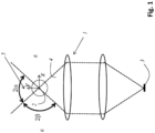
- a detection objective 1 forms the part of the light emanating from a sample area illuminated along a first illumination line 2 Detection light is directed onto a line detector 3, which propagates in a wedge-shaped volume 4 with an aperture angle 2 ⁇ depending on the numerical aperture of the objective 1.
- the first illumination line is perpendicular to the paper plane (z-direction).
- the configuration of the detection beam path and, in particular, of the detection objective 1 defines a detection volume, namely a detection PSF 5 (PSF: point spread function), whereby the detection light emanating from the detection PSF 5 passes through the wedge-shaped volume 4 to the detection objective 1.
- PSF 5 point spread function
- the other illumination line is preferably arranged outside the wedge-shaped volume 4 with the opening angle 2 ⁇ , namely in one of the two wedge-shaped regions 6 with the opening angle 2 ⁇ . This is preferably done in such a way that the other illumination line is arranged in a different sample plane, which allows two different sample planes to be scanned simultaneously by simultaneously shifting the illumination lines laterally, without crosstalk occurring.
- this principle explained using two illumination lines, can also be implemented with a higher number of illumination lines, with adjacent illumination lines being offset in the manner mentioned.
- Crosstalk is advantageously avoided by ensuring that the distance between two adjacent illumination lines is greater than the sum of the illumination beam radius and the radius of the adjacent detection PSF in the plane of the illumination beam.
- the position of the illumination lines is selected such that the illumination beams do not lie in the detection cone (of the detection PSF) of other lines in other planes.
- the present invention allows several sample planes, in particular those parallel to one another, to be scanned simultaneously with at least one illumination line each, wherein the illumination lines are shifted, preferably simultaneously, along the sample planes (i.e., along a vector parallel to a sample plane).
- the illumination lines are arranged offset from one another in a direction along the sample planes and perpendicular to the direction of propagation of the illumination light.
- the illumination lines it is also possible for the illumination lines to be arranged offset from one another in the direction along the sample planes and perpendicular to the optical axis of a detection objective.
- a particularly high image contrast can be achieved by performing a confocal line detection for each illumination line. This is achieved by using a confocally arranged slit detector arrangement achieved.
- the detection light emanating from a sample area illuminated along an illumination line is detected by a detector, in particular an area detector, which is preceded by a slit diaphragm.
- a slit diaphragm can, for example, be formed by an optical element in which a surface leaving a slit is mirrored.
- a mechanical slit diaphragm is complex, however, because when the illumination line is moved, the slit detector arrangement must also be moved at the same time, or alternatively, the detection light must be descanned, for example by means of a beam deflection device arranged in the detection beam path and adjustable with regard to the deflection angle, so that the detection light emanating from the moving illumination line can strike the slit diaphragm. Further details on this can be found below, in particular with reference to the exemplary embodiments.
- the upstream slit diaphragm can be a mechanical shutter curtain, as used in SLR cameras.
- the area detector can be active across its entire sensor area, especially while the slit diaphragm is moving synchronously with the illumination light beam moving along the illumination lines.
- the slit diaphragm can also be particularly advantageously designed as a non-mechanical component.
- the slit diaphragm can be designed as a sectionally switchable mirror or as a sectionally switchable absorber, e.g., based on liquid crystals.
- the detection light emanating from a sample area illuminated along an illumination line to be detected by a detector that functions as a slit detector, wherein the slit detector is formed by the actively switched part of an area detector, for example a CMOS detector or sCMOS detector.
- the slit detector is formed by the actively switched part of an area detector, for example a CMOS detector or sCMOS detector.
- the area detector can remain stationary, in particular relative to the detection objective and/or the illumination objective and/or the sample and/or relative to the incident detection light, with different parts of the sensor surface of the area detector, which then each form the slit detector, being activated in succession; namely, in such a way that only the detection light falling on the activated part is detected, while detection light falling on the parts of the area detector that are respectively deactivated is not detected.
- a region of actively activated pixels can move uniformly and synchronously along the sensor surface of the area detector with an illumination light beam illuminating it along an illumination line.
- a design has the particular advantage of a long service life because movement-related wear, for example of mechanical apertures, is avoided.
- each illuminated sample area is assigned its own detector.
- the detectors assigned to the different sample areas can be arranged in different detection planes, thus taking into account the fact that the sample areas illuminated along a respective illumination line are arranged in different sample planes.
- each illuminated sample area its own detection area on a common area detector.
- a common area detector To ensure that the detection light of all sample areas is focused into the same detection plane, namely the detection plane of the area detector, when using a common area detector, different elements can be used in the different detection beam paths to Adjustment of the optical light path, for example glass blocks of different thicknesses, and/or different focusing or defocusing elements, for example adjustable lenses, can be arranged.
- the detection light emanating from the sample is divided into different detection beam paths by means of at least one beam splitter depending on the location of its origin, i.e. the location of the sample area illuminated by an illumination line.
- the Figure 1 The principle explained above can also be implemented by illuminating the sample simultaneously along at least two adjacent illumination lines, instead of each with its own illumination light beam, with a light sheet that illuminates both illumination light lines simultaneously.
- the light sheet plane is preferably arranged obliquely, i.e. at an angle other than zero degrees to the sample planes.
- crosstalk of the detection light of one illumination line to the detector assigned to the other illumination line can advantageously be reduced.
- the parallel offset ⁇ x of adjacent illumination lines is greater than the sum of the detection PSF radius and half the extension of the light sheet in the direction of the sample plane perpendicular to the light propagation direction, as is Figure 3 illustrated.
- the method according to the invention can be carried out, for example, in such a way that the illumination light is focused by means of an illumination objective and that the detection light emanating from the sample passes through a detection objective, wherein the optical axis of the illumination objective and the optical axis of the detection objective are arranged in mutually perpendicular planes.
- the optical axis of the illumination objective and the optical axis of the detection objective are aligned parallel or coaxially to each other.
- a deflection device can be arranged downstream of the illumination objective, which deflects the illumination light after it has passed through the illumination objective, for example, at a right angle.
- Such a configuration also enables the use of standard upright or inverted microscope stands.
- the microscope according to the invention can advantageously be constructed on the basis of a scanning microscope, in particular a confocal scanning microscope.
- a scanning microscope possibly already available in a laboratory for carrying out the method according to the invention is particularly advantageous in this respect.
- a beam deflection device adjustable in terms of the deflection angle can be used.
- a beam deflection device can, for example, comprise at least one galvanometer mirror.
- the already existing beam deflection device of a scanning microscope, in particular a confocal scanning microscope can also be used; this is particularly true if the microscope according to the invention is manufactured by converting a scanning microscope or the method according to the invention is carried out using a scanning microscope.
- a simple grating or a special diffractive element that generates exactly the desired number of beams and, at the same time, preferably ensures that all illumination light beams are equally bright can be arranged in a plane conjugate to the pupil of the illumination objective. It is important that the desired beam offset along the detection axis is combined with a sufficient offset in the direction of the sample planes. With a grating, this can be achieved by rotating the grating structure in the x-y plane (i.e., around the optical axis of the illumination beam path). Alternatively or additionally, splitting via polarization is also possible using birefringent materials or acousto-optical components.
- the grating can also be flexibly implemented, for example, using an SLM (Spatial Light Modulator).
- chromatic filters in particular chromatic bandpass filters, and/or chromatic beam splitters. take place.
- the microscope according to the invention can advantageously have a control device, in particular an electronic and/or computer-based control device, which synchronously controls the movement of the illumination light illuminating along the illumination lines and/or the movement of the slit detectors or a descanning beam deflection device.
- a control device in particular an electronic and/or computer-based control device, which synchronously controls the movement of the illumination light illuminating along the illumination lines and/or the movement of the slit detectors or a descanning beam deflection device.
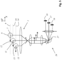
- Fig. 2 shows a schematic representation of the illumination and detection beam path of a first embodiment of a microscope according to the invention.
- a sample is illuminated along a first illumination line 7, which is perpendicular to the plane of the drawing, by means of a first illumination light beam 8 that propagates along the first illumination line 7.
- the first illumination light beam 8 has an illumination light beam radius ⁇ .
- the first illumination line 7 is located in its first sample plane 9.
- a second sample plane 10 which is arranged parallel to the first sample plane 9, the sample is illuminated along a second illumination line 11 by means of a second illumination light beam 12 that propagates along the second illumination line 11.
- the second illumination line 11 is arranged parallel to the first illumination line 7.
- the second illumination line 11 is offset by the amount ⁇ x perpendicular to the optical axis of a detection objective 1, wherein the first sample plane 9 and the second sample plane 10 are spaced apart by a distance ⁇ y.
- the sample is illuminated along a third illumination line 13 in a third sample plane 14 by means of a third illumination light beam 15.
- the detection light emanating from the sample area illuminated by the first illumination light beam 8 is imaged via a detection lens 1 (or detection optics) onto a first line detector 16.
- the detection light emanating from the sample area illuminated by the second illumination light beam 12 is imaged onto a second line detector 17.
- the detection light emanating from the sample area illuminated by the third illumination light beam 15 is imaged onto a third line detector 18.
- the line detectors 16, 17, and 18 are located in different detection planes that are conjugated to the respective illumination planes. In the illustrated embodiment, illumination is performed using three illumination light beams 8, 12, and 15, and detection is performed using three line detectors 16, 17, 18. In principle, however, there is no limit to the number of usable illumination light beams and the number of illuminated sample planes. Therefore, it is also possible to illuminate the sample simultaneously with an even higher number of illumination light beams in an even higher number of sample planes.
- the offset ⁇ x of neighboring illumination lines in the x-direction is chosen such that: ⁇ x > ⁇ + ⁇ .
- the offset ⁇ y of adjacent illumination lines in the y-direction is chosen, for example, such that the sum of the radii r of the corresponding illumination light beams is greater than ⁇ y. (This is in Figure 2 not shown.)
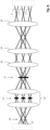
- Figure 3 shows a schematic representation of the illumination and the detection beam path of a second embodiment in which, in contrast to the Figure 2
- the illumination lines 7, 11, 13 are not illuminated with individual, spatially separate illumination light beams 8, 12, 15, but rather with an inclined light sheet 19.
- the light sheet 19 propagates in the direction of the illumination lines 7, 11, 13 (i.e., perpendicular to the plane of the drawing). Due to the inclined position of the light sheet plane of the light sheet 19 relative to the sample planes 9, 10, 14, illumination along the illumination lines 7, 11, 13 arranged in different illumination planes 9, 10, 14 is possible, whereby the use of line detectors also prevents crosstalk, at least to a certain extent.
- This design is not as optically high-quality as the one in Figure 2 illustrated embodiment, because crosstalk can only be avoided to a lesser extent, which is essentially due to the necessarily greater thickness of the light sheet 19.
- Figure 4 shows a schematic representation of the illumination and detection beam path of a third embodiment of a microscope, which does not fall under the terms of the claims.
- the illumination light beam 8, which covers a sample area along a Illumination line 7 in a first sample plane, the second illumination light beam 12 illuminating a second sample region along a second illumination line 11 in a second sample plane 10, and the third illumination light beam 15 illuminating a third sample region along a third illumination line 13 in a third sample plane 14 are simultaneously shifted along the sample planes 9, 10, 14 in order to successively scan each of the sample planes 9, 10, 14 and to result in a 3D stack of data of the sample.
- the detection beam path has a deflection mirror 22, by means of which the detection light emanating from the first sample region illuminated by the first illumination light beam 8 is directed onto a first area detector 23.
- the detection beam path also has a first beam splitter 21, which deflects the detection light emanating from the sample region illuminated by the second illumination light beam 12 onto a second area detector 24.
- the detection beam path also includes a second beam splitter 20, which deflects the detection light emanating from the sample region illuminated by the third illumination light beam 15 to a third area detector 25.
- the area detectors 23, 24, 25 are arranged in such a way that a sharp image of the illuminated sample areas is achieved. During detection, the foci of the respective detection partial light beams move along the surface of the area detectors 23, 24, 25 in accordance with the movement of the illumination light beams 8, 10, 15. It can advantageously be provided that only a narrow strip of each area detector 23, 24, 25 is activated, while the neighboring areas are each deactivated. In this way, a slit detector is realized in each case, which allows confocal detection.
- a movement of the respectively active part of the respective area detector 23, 24, 25 can be realized, thus creating a type of "rolling shutter," i.e., a slit detector arrangement that moves synchronously with the movement of the illuminating light beams 8, 12, 15.
- a particularly advantageous subclass of this method consists in exciting different fluorophores in different sample planes, for example, with different laser lines. Subsequently, a separation in the detection beam path can be achieved with the aid of of chromatic filters, in particular chromatic bandpass filters, and/or with the help of chromatic beam splitters.
- FIG. 5 shows a schematic representation of the illumination and detection beam path of a fourth embodiment.
- a beam deflection device 26 adjustable in terms of deflection angle, is located in the detection beam path.
- This beam deflection device includes a mirror 27 rotatably mounted by means of a galvanometer drive.
- the beam deflection device is controlled synchronously with the movement of the illumination light beams 8, 10, 12 such that the foci of the detection light, unlike in the Figure 4
- the beams do not migrate on the surface of the line detectors 16, 17, 18, but rather remain stationary.
- Such a design has the particular advantage that, in particular, fixed mechanical apertures can also be used.
- Figure 6 shows a schematic representation of the illumination and detection beam path of a fifth embodiment of a microscope according to the invention.
- a single area detector 28 is present, with each illuminated sample area being assigned its own detection area on the common area detector 28.
- a means 29 for influencing the optical path length is arranged in each of the partial detection beam paths.
- This means consists of a first, thinner glass block 30, a second, slightly thicker glass block 31, and a third, even thicker glass block 32.
- the glass blocks can have a correspondingly shaped surface to avoid aberrations, in particular spherical aberrations.
- Figure 7 shows a schematic representation of the illumination and beam path of a sixth embodiment of a microscope, which does not fall under the terms of the claims.
- This embodiment includes a further beam deflection device in the detection beam path, the deflection angle of which is adjustable, in order to rescan the strip images filtered by confocal apertures 33 synchronously with the movement of the illumination light beams 8, 12, 15. This allows confocal image data of the individual sample planes to be recorded directly with one area detector 23, 24, 25 each, without the need for continuous spatial activation.
- Figure 8 shows schematically an example of an arrangement for generating a plurality of illumination light beams 8, 12, 15 for simultaneous illumination along a plurality of offset illumination lines.
- the arrangement comprises a grating 34 which forms a primary Illumination light beam 35, which can in particular be generated by a laser light source, is spatially split.
- Illumination light beams 8, 12, 15 then pass through a telescope arrangement 36, which can additionally include a filter 41.
- a beam deflection device 37 the deflection angle of which can be adjusted in order to be able to move the illumination light beams 8, 12, 15 in their respective sample planes.
- the illumination light beams 8, 12, 15 coming from the beam deflection device 37 pass through a scanning lens 38, a tube lens 39, and finally reach the illumination objective 40. After passing through the illumination objective 40, the illumination light beams 8, 12, 15 reach the sample (not shown here) directly or after further deflection.
Landscapes
- Physics & Mathematics (AREA)
- Chemical & Material Sciences (AREA)
- Analytical Chemistry (AREA)
- General Physics & Mathematics (AREA)
- Optics & Photonics (AREA)
- Engineering & Computer Science (AREA)
- Multimedia (AREA)
- Computer Vision & Pattern Recognition (AREA)
- Microscoopes, Condenser (AREA)
- Investigating, Analyzing Materials By Fluorescence Or Luminescence (AREA)
Claims (18)
- Procédé d'analyse d'un échantillon, dans lequel l'échantillon est éclairé simultanément dans plusieurs plans d'échantillon (9, 10, 14) différents les uns des autres respectivement le long d'une ligne d'éclairage (7, 11, 13) avec respectivement un faisceau lumineux d'éclairage (8, 12, 15) et dans lequel chaque zone d'échantillon éclairée le long d'une ligne d'éclairage (7, 11, 13) est balayée à l'aide d'un seul et même objectif de détection (1) chacune avec sa propre PSF de détection et la lumière de détection émanant des zones d'échantillon éclairées est détectée simultanément et séparément dans l'espace, et dans lequel soitla lumière de détection émanant des zones d'échantillon éclairées est détectée à l'aide de détecteurs linéaires (16, 17, 18) qui se situent dans différents plans de détection qui sont conjugués aux plans d'éclairage respectifs ; soitdans lequel la lumière de détection émanant des zones d'échantillon éclairées est détectée à l'aide d'un détecteur de surface (28), dans lequel une zone de détection propre est attribuée à chaque zone d'échantillon éclairée sur le détecteur de surface (28), et dans lequel un moyen (29) d'influence de la longueur de chemin optique est agencé dans chaque chemin de faisceau de détection partiel.
- Procédé selon la revendication 1, caractérisé en ce que des plans d'échantillon (9, 10, 14) sont orientés parallèlement les uns aux autres.
- Procédé selon la revendication 1 ou 2, caractérisé en ce quea. les lignes d'éclairage (7, 11, 13) sont disposées décalées les unes par rapport aux autres dans une direction le long des plans d'échantillon (9, 10, 14) et perpendiculairement au sens de propagation de la lumière d'éclairage des faisceaux lumineux d'éclairage (8, 12, 15), et/ou en ce queb. les lignes d'éclairage (7, 11, 13) sont disposées décalées les unes par rapport aux autres dans un sens le long des plans d'échantillon (9, 10, 14) et perpendiculairement à l'axe optique de l'objectif de détection (1), et/ou en ce quec. aucune autre des lignes d'éclairage (7, 11, 13) n'est disposée dans le faisceau lumineux de détection émanant d'une zone d'échantillon éclairée avec une ligne d'éclairage (7, 11, 13).
- Procédé selon l'une quelconque des revendications 1 à 3, caractérisé en ce que chacun des plans d'échantillon (9, 10, 14) est balayé successivement par déplacement synchrone, en particulier déplacement parallèle, du faisceau lumineux d'éclairage (8, 12, 15) respectif et de la PSF de détection respective.
- Procédé selon l'une quelconque des revendications 1 à 4, caractérisé en ce quea. une détection de ligne confocale est réalisée et/ou en ce queb. la lumière de détection émanant respectivement d'une zone d'échantillon éclairée le long d'une ligne d'éclairage (7, 11, 13) est détectée par un détecteur, en amont duquel est placé un diaphragme à fente, et/ou en ce quec. la lumière de détection émanant respectivement d'une zone d'échantillon éclairée le long d'une ligne d'éclairage (7, 11, 13) est détectée par un détecteur qui fonctionne comme détecteur à fente, dans lequel le détecteur à fente est formé par la partie respectivement activée d'un détecteur de surface.
- Procédé selon l'une quelconque des revendications 1 à 5, caractérisé en ce qu'un détecteur propre est attribué à chaque zone d'échantillon éclairée ou en ce qu'une zone de détection propre est attribuée à chaque zone d'échantillon éclairée sur un détecteur de surface commun.
- Procédé selon l'une quelconque des revendications 1 à 6, caractérisé en ce que la lumière de détection émanant de l'échantillon est répartie en fonction du lieu de sa formation au moyen d'au moins un séparateur de faisceau (20, 21) sur différentes branches de chemin de faisceau de détection.
- Procédé selon l'une quelconque des revendications 1 à 7, caractérisé en ce quea. l'échantillon est éclairé simultanément au moins le long de deux lignes d'éclairage (7, 11, 13) adjacentes plutôt qu'avec respectivement un faisceau lumineux d'éclairage (8, 12, 15) propre avec une feuille lumineuse (19), et/ou en ce queb. l'échantillon est éclairé simultanément au moins le long de deux lignes d'éclairage (7, 11, 13) adjacentes plutôt qu'avec respectivement un faisceau lumineux d'éclairage (8, 12, 15) propre avec une feuille lumineuse (19), dans lequel l'écart des lignes d'éclairage (7, 11, 13) est supérieur à la somme du rayon de PSF de détection (δ) et de la demi-extension de la feuille lumineuse dans le sens du plan d'échantillon perpendiculairement au sens de propagation de la lumière.
- Procédé selon l'une quelconque des revendications 1 à 8, caractérisé en ce quea. la lumière d'éclairage est focalisée au moyen d'un objectif d'éclairage (40) et en ce que la lumière de détection émanant de l'échantillon traverse l'objectif de détection (1), dans lequel l'axe optique de l'objectif d'éclairage (40) et l'axe optique de l'objectif de détection (1) sont disposés dans des plans perpendiculaires l'un par rapport à l'autre, ou en ce queb. la lumière d'éclairage est focalisée au moyen d'un objectif d'éclairage (40) et en ce que la lumière de détection émanant de l'échantillon traverse l'objectif de détection (1), dans lequel l'axe optique de l'objectif d'éclairage (40) et l'axe optique de l'objectif de détection (1) sont orientés parallèlement ou coaxialement l'un par rapport à l'autre.
- Microscope pour la mise en œuvre d'un procédé selon l'une quelconque des revendications 1 à 9, caractérisé par un agencement d'éclairage qui présente un objectif d'éclairage (40) et qui est conçu pour éclairer simultanément un échantillon dans plusieurs plans d'échantillon (9, 10, 14) différents les uns des autres respectivement le long d'une ligne d'éclairage (7, 11, 13) avec respectivement un faisceau lumineux d'éclairage (8, 12, 15), et caractérisé par un agencement de détection qui présente un objectif de détection (1) et au moins un détecteur et qui est conçu pour que chaque zone d'échantillon éclairée le long d'une ligne d'éclairage (7, 11, 13) soit balayée à l'aide de l'objectif de détection (1) respectivement avec une PSF de détection propre et que la lumière de détection émanant des zones d'échantillon éclairées soit détectée simultanément et séparément dans l'espace,dans lequel soit le microscope comprend des détecteurs linéaires (16, 17, 18) qui sont conçus pour détecter la lumière de détection émanant des zones d'échantillon éclairées et qui se situent dans différents niveaux de détection qui sont conjugués aux plans d'éclairage respectifs ; soitdans lequel le microscope comprend un détecteur de surface (28) qui est conçu pour détecter la lumière de détection émanant des zones d'échantillon éclairées, dans lequel une zone de détection propre est attribuée à chaque zone d'échantillon éclairée sur le détecteur de surface (28), et dans lequel un moyen (29) pour l'influence de la longueur de chemin optique est agencé dans chaque chemin de faisceau de détection partiel.
- Microscope selon la revendication 10, caractérisé en ce que des plans d'échantillon (9, 10, 14) sont orientés parallèlement les uns aux autres.
- Microscope selon la revendication 10 ou 11, caractérisé en ce quea. des lignes d'éclairage sont disposées décalées les unes par rapport aux autres dans un sens le long des plans d'échantillon (9, 10, 14) et perpendiculairement au sens de propagation de la lumière d'éclairage des faisceaux lumineux d'éclairage (8, 12, 15), et/ou en ce queb. les lignes d'éclairage (7, 11, 13) sont disposées décalées les unes par rapport aux autres dans un sens le long des plans d'échantillon (9, 10, 14) et perpendiculairement à l'axe optique de l'objectif de détection (1), et/ou en ce quec. aucune autre des lignes d'éclairage (7, 11, 13) n'est disposée dans le faisceau lumineux de détection émanant d'une zone d'échantillon éclairée avec une ligne d'éclairage (7, 11, 13).
- Procédé selon l'une quelconque des revendications 10 à 12, caractérisé en ce quea. l'agencement d'éclairage présente un dispositif de déviation de faisceau (26) réglable en ce qui concerne l'angle de déviation, au moyen duquel les faisceaux lumineux d'éclairage (8, 12, 15) peuvent être déplacés parallèlement, et/ou en ce queb. l'agencement de détection présente un dispositif de déviation de faisceau (26) réglable en ce qui concerne l'angle de déviation, qui entraîne un déscannage de la lumière de détection.
- Microscope selon l'une quelconque des revendications 10 à 13, caractérisé en ce qu'un détecteur propre est attribué à chaque zone d'échantillon éclairée ou en ce qu'une zone de détection propre est attribuée à chaque zone d'échantillon éclairée sur un détecteur de surface commun.
- Microscope selon l'une quelconque des revendications 10 à 14, caractérisé en ce quea. une détection de ligne confocale est réalisée et/ou en ce queb. la lumière de détection émanant respectivement d'une zone d'échantillon éclairée le long d'une ligne d'éclairage (7, 11, 13) est détectée par un détecteur, en amont duquel est placé un diaphragme à fente, et/ou en ce quec. la lumière de détection émanant respectivement d'une zone d'échantillon éclairée le long d'une ligne d'éclairage (7, 11, 13) est détectée par un détecteur qui fonctionne comme détecteur à fente, dans lequel le détecteur à fente s'étend à travers la partie respectivement activée d'un détecteur de surface.
- Microscope selon l'une quelconque des revendications 10 à 15, caractérisé en ce que l'agencement de détection présente au moins un séparateur de faisceau (20, 21) qui répartit la lumière de détection émanant de l'échantillon en fonction du lieu de sa formation sur différentes branches de chemin de faisceau de détection.
- Microscope selon l'une quelconque des revendications 10 à 16, caractérisé en ce quea. l'agencement d'éclairage génère une feuille lumineuse (19) qui, au lieu d'un éclairage avec respectivement un faisceau lumineux d'éclairage (8, 12, 15) propre, éclaire simultanément l'échantillon à examiner le long d'au moins deux lignes d'éclairage (7, 11, 13) adjacentes, et/ou en ce queb. l'agencement d'éclairage génère une feuille lumineuse (19) qui, au lieu d'un éclairage avec respectivement un faisceau lumineux d'éclairage (8, 12, 15) propre, éclaire simultanément l'échantillon à examiner le long d'au moins deux lignes d'éclairage (7, 11, 13) adjacentes,dans lequel la distance entre les lignes d'éclairage (7, 11, 13) est supérieure à la somme du rayon de PSF de détection et de la demi-extension de la feuille lumineuse dans le sens du plan d'échantillon (9, 10, 14) perpendiculairement au sens de propagation de la lumière.
- Microscope selon l'une quelconque des revendications 10 à 17, caractérisé en ce quea. l'axe optique de l'objectif d'éclairage (40) et l'axe optique de l'objectif de détection (1) sont disposés dans des plans perpendiculaires l'un par rapport à l'autre, ou en ce queb. l'axe optique de l'objectif d'éclairage (40) et l'axe optique de l'objectif de détection (1) sont orientés parallèlement ou coaxialement l'un par rapport à l'autre.
Applications Claiming Priority (2)
| Application Number | Priority Date | Filing Date | Title |
|---|---|---|---|
| LU93022A LU93022B1 (de) | 2016-04-08 | 2016-04-08 | Verfahren und Mikroskop zum Untersuchen einer Probe |
| PCT/EP2017/058420 WO2017174792A1 (fr) | 2016-04-08 | 2017-04-07 | Procédé et dispositif d'analyse d'un échantillon |
Publications (2)
| Publication Number | Publication Date |
|---|---|
| EP3440492A1 EP3440492A1 (fr) | 2019-02-13 |
| EP3440492B1 true EP3440492B1 (fr) | 2025-03-12 |
Family
ID=55967355
Family Applications (1)
| Application Number | Title | Priority Date | Filing Date |
|---|---|---|---|
| EP17717127.9A Active EP3440492B1 (fr) | 2016-04-08 | 2017-04-07 | Procédé et dispositif d'analyse d'un échantillon |
Country Status (6)
| Country | Link |
|---|---|
| US (1) | US10459209B2 (fr) |
| EP (1) | EP3440492B1 (fr) |
| JP (1) | JP7094225B2 (fr) |
| CN (1) | CN108885336B (fr) |
| LU (1) | LU93022B1 (fr) |
| WO (1) | WO2017174792A1 (fr) |
Families Citing this family (4)
| Publication number | Priority date | Publication date | Assignee | Title |
|---|---|---|---|---|
| CN110914673B (zh) * | 2017-04-20 | 2023-10-24 | 生物梅里埃公司 | 光密度仪器及使用光密度仪器的系统和方法 |
| DE102018204940B4 (de) * | 2018-03-29 | 2023-03-30 | Leica Microsystems Cms Gmbh | Optisches System mit verkippter Beleuchtungsebene und Verfahren zum Beleuchten eines Probenvolumens in einem optischen System mit verkippter Beleuchtungsebene |
| EP3627205A1 (fr) * | 2018-09-20 | 2020-03-25 | Koninklijke Philips N.V. | Microscope confocal à balayage laser conçu pour générer des foyers linéaires |
| JP7803048B2 (ja) * | 2021-06-17 | 2026-01-21 | 日本精工株式会社 | 三次元検出顕微鏡システム |
Family Cites Families (25)
| Publication number | Priority date | Publication date | Assignee | Title |
|---|---|---|---|---|
| EP1064579A4 (fr) * | 1998-03-16 | 2007-11-07 | Praelux Inc | Systeme d'imagerie confocal pour microscopie |
| KR20010083041A (ko) * | 1998-06-02 | 2001-08-31 | 추후 | 파수 도메인 반사측정과 배경 진폭 감소 및 보상을 사용한공초점 간섭 마이크로스코피용 방법 및 장치 |
| JP4488259B2 (ja) * | 1999-09-13 | 2010-06-23 | オリンパス株式会社 | 量子ドット観察装置 |
| JP2003043365A (ja) * | 2001-07-30 | 2003-02-13 | Japan Science & Technology Corp | 断層面観測装置 |
| DE10257423A1 (de) | 2002-12-09 | 2004-06-24 | Europäisches Laboratorium für Molekularbiologie (EMBL) | Mikroskop |
| DE102007018048A1 (de) * | 2007-04-13 | 2008-10-16 | Michael Schwertner | Verfahren und Anordnung zur optischen Abbildung mit Tiefendiskriminierung |
| DE102009044983A1 (de) | 2009-09-24 | 2011-03-31 | Carl Zeiss Microimaging Gmbh | Mikroskop |
| DE102010060121C5 (de) * | 2010-10-22 | 2023-09-28 | Leica Microsystems Cms Gmbh | SPIM-Mikroskop mit sequenziellem Lightsheet |
| DE102011003603B4 (de) * | 2011-02-03 | 2019-12-24 | Leica Microsystems (Schweiz) Ag | Durchlichtbeleuchtungseinrichtung für ein Mikroskop |
| US10908403B2 (en) * | 2011-02-14 | 2021-02-02 | European Molecular Biology Laboratory (Embl) | Light-pad microscope for high-resolution 3D fluorescence imaging and 2D fluctuation spectroscopy |
| DE102011051042B4 (de) * | 2011-06-14 | 2016-04-28 | Leica Microsystems Cms Gmbh | Abtastmikroskop und Verfahren zur lichtmikroskopischen Abbildung eines Objektes |
| DE102011055426B4 (de) * | 2011-11-16 | 2026-03-19 | Miltenyi Imaging Gmbh | Mikroskopieverfahren zur Erkennung biologischer Zielobjekte |
| WO2013090360A2 (fr) * | 2011-12-15 | 2013-06-20 | President And Fellows Of Harvard College | Microscopie haute résolution à double objectif |
| ITPI20120034A1 (it) * | 2012-03-31 | 2013-10-01 | Cnr Consiglio Naz Delle Ricer Che | Metodo e dispositivo perfezionati per microscopia video-confocale |
| DE102012009836A1 (de) * | 2012-05-16 | 2013-11-21 | Carl Zeiss Microscopy Gmbh | Lichtmikroskop und Verfahren zur Bildaufnahme mit einem Lichtmikroskop |
| DE102012214568A1 (de) * | 2012-08-16 | 2014-02-20 | Leica Microsystems Cms Gmbh | Optische Anordnung und ein Mikroskop |
| DE102013213781A1 (de) * | 2013-03-20 | 2014-09-25 | Leica Microsystems Cms Gmbh | Verfahren und optische Anordnung zum Manipulieren und Abbilden einer mikroskopischen Probe |
| DE102013205115A1 (de) | 2013-03-22 | 2014-09-25 | Leica Microsystems Cms Gmbh | SPIM-Anordnung |
| US9229213B2 (en) * | 2013-05-24 | 2016-01-05 | Steven E. Richfield | Coincident focus microscope having superior resolution and contrast in three dimensions |
| DE102013211426A1 (de) * | 2013-06-18 | 2014-12-18 | Leica Microsystems Cms Gmbh | Verfahren und optische Vorrichtung zum mikroskopischen Untersuchen einer Vielzahl von Proben |
| DE102013016367A1 (de) * | 2013-09-30 | 2015-04-02 | Carl Zeiss Microscopy Gmbh | Lichtmikroskop und Verfahren zum Untersuchen einer Probe mit einem Lichtmikroskop |
| US10539772B2 (en) * | 2013-10-09 | 2020-01-21 | Howard Hughes Medical Institute | Multiview light-sheet microscopy |
| CN103645136A (zh) * | 2013-11-22 | 2014-03-19 | 深圳先进技术研究院 | 一种提高多光子荧光显微镜成像分辨率的方法及装置 |
| KR20170013855A (ko) * | 2014-05-30 | 2017-02-07 | 더 보드 오브 트러스티스 오브 더 리랜드 스탠포드 쥬니어 유니버시티 | 큰 손상되지 않은 조직 샘플들을 이미징하기 위한 방법들 및 디바이스들 |
| CN105486667A (zh) * | 2015-07-01 | 2016-04-13 | 上海睿钰生物科技有限公司 | 集成式荧光激发光源装置 |
-
2016
- 2016-04-08 LU LU93022A patent/LU93022B1/de active IP Right Grant
-
2017
- 2017-04-07 EP EP17717127.9A patent/EP3440492B1/fr active Active
- 2017-04-07 WO PCT/EP2017/058420 patent/WO2017174792A1/fr not_active Ceased
- 2017-04-07 JP JP2018552762A patent/JP7094225B2/ja active Active
- 2017-04-07 US US16/091,522 patent/US10459209B2/en active Active
- 2017-04-07 CN CN201780020220.2A patent/CN108885336B/zh active Active
Also Published As
| Publication number | Publication date |
|---|---|
| CN108885336B (zh) | 2021-12-14 |
| WO2017174792A1 (fr) | 2017-10-12 |
| JP7094225B2 (ja) | 2022-07-01 |
| US10459209B2 (en) | 2019-10-29 |
| US20190129156A1 (en) | 2019-05-02 |
| CN108885336A (zh) | 2018-11-23 |
| LU93022B1 (de) | 2017-11-08 |
| JP2019514060A (ja) | 2019-05-30 |
| EP3440492A1 (fr) | 2019-02-13 |
Similar Documents
| Publication | Publication Date | Title |
|---|---|---|
| EP2860566B1 (fr) | Microscopie à balayage haute résolution | |
| DE102018210603B4 (de) | Verfahren zum Erzeugen eines Übersichtsbilds unter Verwendung eines hochaperturigen Objektivs | |
| DE10063276C2 (de) | Scanmikroskop | |
| DE102016119268B3 (de) | Schiefebenenmikroskop | |
| EP3084399B1 (fr) | Dispositif et procédé d'analyse d'un échantillon par tomographie optique de projection | |
| EP3173838A1 (fr) | Microscope à feuille de lumière | |
| DE102020209889A1 (de) | Mikroskop und Verfahren zur mikroskopischen Bildaufnahme mit variabler Beleuchtung | |
| DE102013022538B3 (de) | Verfahren zum Erstellen eines Mikroskopbildes und Mikroskopievorrichtung | |
| EP3283917B2 (fr) | Procédé et dispositif d'analyse d'un échantillon | |
| DE10038622A1 (de) | Scan-Mikroskop,optische Anordnung und Verfahren zur Bildaufnahme in der Scan-Mikroskopie | |
| DE102015209756A1 (de) | Anordnung und Verfahren zur Lichtblattmikroskopie | |
| EP3440491B1 (fr) | Microscope et procédé de reproduction d'un échantillon | |
| LU92925B1 (de) | Verfahren zum Untersuchen einer Probe mittels Lichtblatt-Mikroskopie und Lichtblatt-Mikroskop | |
| EP3475750B1 (fr) | Dispositif d'éclairage pour un microscope | |
| EP3828616A1 (fr) | Procédé d'ajustement d'un microscope à fluorescence - scanner laser et microscope à fluorescence - scanner laser comprenant un appareil d'ajustement automatique | |
| EP4453627B1 (fr) | Microscope et procédé pour microscopie | |
| EP1664888A1 (fr) | Microscope a balayage avec eclairage evanescent | |
| EP1128200A2 (fr) | Structure de microscope | |
| DE102023100926A1 (de) | Mikroskop | |
| LU93022B1 (de) | Verfahren und Mikroskop zum Untersuchen einer Probe | |
| DE102023005252A1 (de) | Mikroskop mit schneller quasikonfokaler Detektion | |
| EP3482247B1 (fr) | Procédé d'analyse d'un échantillon et dispositif permettant la mise en oeuvre dudit procédé | |
| DE102004029733A1 (de) | Rastermikroskop und Verfahren zur Rastermikroskopie | |
| DE102018126009A1 (de) | Verfahren und Mikroskop zur Bestimmung der Dicke eines Deck- oder Tragglases | |
| DE102017116436A1 (de) | Anordnung zur Einkopplung von Beleuchtungsstrahlung und Auskopplung von einer Probe zurückkommender Strahlung in einen Mikroskopstrahlengang |
Legal Events
| Date | Code | Title | Description |
|---|---|---|---|
| STAA | Information on the status of an ep patent application or granted ep patent |
Free format text: STATUS: UNKNOWN |
|
| STAA | Information on the status of an ep patent application or granted ep patent |
Free format text: STATUS: THE INTERNATIONAL PUBLICATION HAS BEEN MADE |
|
| PUAI | Public reference made under article 153(3) epc to a published international application that has entered the european phase |
Free format text: ORIGINAL CODE: 0009012 |
|
| STAA | Information on the status of an ep patent application or granted ep patent |
Free format text: STATUS: REQUEST FOR EXAMINATION WAS MADE |
|
| 17P | Request for examination filed |
Effective date: 20181108 |
|
| AK | Designated contracting states |
Kind code of ref document: A1 Designated state(s): AL AT BE BG CH CY CZ DE DK EE ES FI FR GB GR HR HU IE IS IT LI LT LU LV MC MK MT NL NO PL PT RO RS SE SI SK SM TR |
|
| AX | Request for extension of the european patent |
Extension state: BA ME |
|
| DAV | Request for validation of the european patent (deleted) | ||
| DAX | Request for extension of the european patent (deleted) | ||
| STAA | Information on the status of an ep patent application or granted ep patent |
Free format text: STATUS: EXAMINATION IS IN PROGRESS |
|
| 17Q | First examination report despatched |
Effective date: 20211015 |
|
| P01 | Opt-out of the competence of the unified patent court (upc) registered |
Effective date: 20230414 |
|
| GRAP | Despatch of communication of intention to grant a patent |
Free format text: ORIGINAL CODE: EPIDOSNIGR1 |
|
| STAA | Information on the status of an ep patent application or granted ep patent |
Free format text: STATUS: GRANT OF PATENT IS INTENDED |
|
| INTG | Intention to grant announced |
Effective date: 20240717 |
|
| GRAJ | Information related to disapproval of communication of intention to grant by the applicant or resumption of examination proceedings by the epo deleted |
Free format text: ORIGINAL CODE: EPIDOSDIGR1 |
|
| STAA | Information on the status of an ep patent application or granted ep patent |
Free format text: STATUS: EXAMINATION IS IN PROGRESS |
|
| GRAP | Despatch of communication of intention to grant a patent |
Free format text: ORIGINAL CODE: EPIDOSNIGR1 |
|
| STAA | Information on the status of an ep patent application or granted ep patent |
Free format text: STATUS: GRANT OF PATENT IS INTENDED |
|
| INTC | Intention to grant announced (deleted) | ||
| INTG | Intention to grant announced |
Effective date: 20241023 |
|
| GRAS | Grant fee paid |
Free format text: ORIGINAL CODE: EPIDOSNIGR3 |
|
| GRAA | (expected) grant |
Free format text: ORIGINAL CODE: 0009210 |
|
| STAA | Information on the status of an ep patent application or granted ep patent |
Free format text: STATUS: THE PATENT HAS BEEN GRANTED |
|
| AK | Designated contracting states |
Kind code of ref document: B1 Designated state(s): AL AT BE BG CH CY CZ DE DK EE ES FI FR GB GR HR HU IE IS IT LI LT LU LV MC MK MT NL NO PL PT RO RS SE SI SK SM TR |
|
| REG | Reference to a national code |
Ref country code: GB Ref legal event code: FG4D Free format text: NOT ENGLISH |
|
| REG | Reference to a national code |
Ref country code: CH Ref legal event code: EP |
|
| REG | Reference to a national code |
Ref country code: DE Ref legal event code: R096 Ref document number: 502017016738 Country of ref document: DE |
|
| REG | Reference to a national code |
Ref country code: IE Ref legal event code: FG4D Free format text: LANGUAGE OF EP DOCUMENT: GERMAN |
|
| PG25 | Lapsed in a contracting state [announced via postgrant information from national office to epo] |
Ref country code: RS Free format text: LAPSE BECAUSE OF FAILURE TO SUBMIT A TRANSLATION OF THE DESCRIPTION OR TO PAY THE FEE WITHIN THE PRESCRIBED TIME-LIMIT Effective date: 20250612 |
|
| PG25 | Lapsed in a contracting state [announced via postgrant information from national office to epo] |
Ref country code: FI Free format text: LAPSE BECAUSE OF FAILURE TO SUBMIT A TRANSLATION OF THE DESCRIPTION OR TO PAY THE FEE WITHIN THE PRESCRIBED TIME-LIMIT Effective date: 20250312 |
|
| PGFP | Annual fee paid to national office [announced via postgrant information from national office to epo] |
Ref country code: DE Payment date: 20250428 Year of fee payment: 9 |
|
| PG25 | Lapsed in a contracting state [announced via postgrant information from national office to epo] |
Ref country code: ES Free format text: LAPSE BECAUSE OF FAILURE TO SUBMIT A TRANSLATION OF THE DESCRIPTION OR TO PAY THE FEE WITHIN THE PRESCRIBED TIME-LIMIT Effective date: 20250312 |
|
| PGFP | Annual fee paid to national office [announced via postgrant information from national office to epo] |
Ref country code: GB Payment date: 20250422 Year of fee payment: 9 |
|
| REG | Reference to a national code |
Ref country code: LT Ref legal event code: MG9D |
|
| PG25 | Lapsed in a contracting state [announced via postgrant information from national office to epo] |
Ref country code: NO Free format text: LAPSE BECAUSE OF FAILURE TO SUBMIT A TRANSLATION OF THE DESCRIPTION OR TO PAY THE FEE WITHIN THE PRESCRIBED TIME-LIMIT Effective date: 20250612 |
|
| PG25 | Lapsed in a contracting state [announced via postgrant information from national office to epo] |
Ref country code: HR Free format text: LAPSE BECAUSE OF FAILURE TO SUBMIT A TRANSLATION OF THE DESCRIPTION OR TO PAY THE FEE WITHIN THE PRESCRIBED TIME-LIMIT Effective date: 20250312 |
|
| REG | Reference to a national code |
Ref country code: NL Ref legal event code: MP Effective date: 20250312 |
|
| PG25 | Lapsed in a contracting state [announced via postgrant information from national office to epo] |
Ref country code: LV Free format text: LAPSE BECAUSE OF FAILURE TO SUBMIT A TRANSLATION OF THE DESCRIPTION OR TO PAY THE FEE WITHIN THE PRESCRIBED TIME-LIMIT Effective date: 20250312 |
|
| PGFP | Annual fee paid to national office [announced via postgrant information from national office to epo] |
Ref country code: FR Payment date: 20250424 Year of fee payment: 9 |
|
| PG25 | Lapsed in a contracting state [announced via postgrant information from national office to epo] |
Ref country code: BG Free format text: LAPSE BECAUSE OF FAILURE TO SUBMIT A TRANSLATION OF THE DESCRIPTION OR TO PAY THE FEE WITHIN THE PRESCRIBED TIME-LIMIT Effective date: 20250312 Ref country code: GR Free format text: LAPSE BECAUSE OF FAILURE TO SUBMIT A TRANSLATION OF THE DESCRIPTION OR TO PAY THE FEE WITHIN THE PRESCRIBED TIME-LIMIT Effective date: 20250613 |
|
| PG25 | Lapsed in a contracting state [announced via postgrant information from national office to epo] |
Ref country code: NL Free format text: LAPSE BECAUSE OF FAILURE TO SUBMIT A TRANSLATION OF THE DESCRIPTION OR TO PAY THE FEE WITHIN THE PRESCRIBED TIME-LIMIT Effective date: 20250312 |
|
| PG25 | Lapsed in a contracting state [announced via postgrant information from national office to epo] |
Ref country code: SE Free format text: LAPSE BECAUSE OF FAILURE TO SUBMIT A TRANSLATION OF THE DESCRIPTION OR TO PAY THE FEE WITHIN THE PRESCRIBED TIME-LIMIT Effective date: 20250312 |
|
| PG25 | Lapsed in a contracting state [announced via postgrant information from national office to epo] |
Ref country code: SM Free format text: LAPSE BECAUSE OF FAILURE TO SUBMIT A TRANSLATION OF THE DESCRIPTION OR TO PAY THE FEE WITHIN THE PRESCRIBED TIME-LIMIT Effective date: 20250312 |
|
| PG25 | Lapsed in a contracting state [announced via postgrant information from national office to epo] |
Ref country code: PT Free format text: LAPSE BECAUSE OF FAILURE TO SUBMIT A TRANSLATION OF THE DESCRIPTION OR TO PAY THE FEE WITHIN THE PRESCRIBED TIME-LIMIT Effective date: 20250714 |
|
| PG25 | Lapsed in a contracting state [announced via postgrant information from national office to epo] |
Ref country code: PL Free format text: LAPSE BECAUSE OF FAILURE TO SUBMIT A TRANSLATION OF THE DESCRIPTION OR TO PAY THE FEE WITHIN THE PRESCRIBED TIME-LIMIT Effective date: 20250312 Ref country code: IT Free format text: LAPSE BECAUSE OF FAILURE TO SUBMIT A TRANSLATION OF THE DESCRIPTION OR TO PAY THE FEE WITHIN THE PRESCRIBED TIME-LIMIT Effective date: 20250312 |
|
| PG25 | Lapsed in a contracting state [announced via postgrant information from national office to epo] |
Ref country code: EE Free format text: LAPSE BECAUSE OF FAILURE TO SUBMIT A TRANSLATION OF THE DESCRIPTION OR TO PAY THE FEE WITHIN THE PRESCRIBED TIME-LIMIT Effective date: 20250312 Ref country code: CZ Free format text: LAPSE BECAUSE OF FAILURE TO SUBMIT A TRANSLATION OF THE DESCRIPTION OR TO PAY THE FEE WITHIN THE PRESCRIBED TIME-LIMIT Effective date: 20250312 |
|
| PG25 | Lapsed in a contracting state [announced via postgrant information from national office to epo] |
Ref country code: RO Free format text: LAPSE BECAUSE OF FAILURE TO SUBMIT A TRANSLATION OF THE DESCRIPTION OR TO PAY THE FEE WITHIN THE PRESCRIBED TIME-LIMIT Effective date: 20250312 |
|
| PG25 | Lapsed in a contracting state [announced via postgrant information from national office to epo] |
Ref country code: SK Free format text: LAPSE BECAUSE OF FAILURE TO SUBMIT A TRANSLATION OF THE DESCRIPTION OR TO PAY THE FEE WITHIN THE PRESCRIBED TIME-LIMIT Effective date: 20250312 |
|
| PG25 | Lapsed in a contracting state [announced via postgrant information from national office to epo] |
Ref country code: IS Free format text: LAPSE BECAUSE OF FAILURE TO SUBMIT A TRANSLATION OF THE DESCRIPTION OR TO PAY THE FEE WITHIN THE PRESCRIBED TIME-LIMIT Effective date: 20250712 |
|
| REG | Reference to a national code |
Ref country code: CH Ref legal event code: H13 Free format text: ST27 STATUS EVENT CODE: U-0-0-H10-H13 (AS PROVIDED BY THE NATIONAL OFFICE) Effective date: 20251125 |
|
| PG25 | Lapsed in a contracting state [announced via postgrant information from national office to epo] |
Ref country code: LU Free format text: LAPSE BECAUSE OF NON-PAYMENT OF DUE FEES Effective date: 20250407 |
|
| REG | Reference to a national code |
Ref country code: DE Ref legal event code: R097 Ref document number: 502017016738 Country of ref document: DE |
|
| PG25 | Lapsed in a contracting state [announced via postgrant information from national office to epo] |
Ref country code: MC Free format text: LAPSE BECAUSE OF FAILURE TO SUBMIT A TRANSLATION OF THE DESCRIPTION OR TO PAY THE FEE WITHIN THE PRESCRIBED TIME-LIMIT Effective date: 20250312 |
|
| REG | Reference to a national code |
Ref country code: BE Ref legal event code: MM Effective date: 20250430 |
|
| PG25 | Lapsed in a contracting state [announced via postgrant information from national office to epo] |
Ref country code: DK Free format text: LAPSE BECAUSE OF FAILURE TO SUBMIT A TRANSLATION OF THE DESCRIPTION OR TO PAY THE FEE WITHIN THE PRESCRIBED TIME-LIMIT Effective date: 20250312 |
|
| PG25 | Lapsed in a contracting state [announced via postgrant information from national office to epo] |
Ref country code: BE Free format text: LAPSE BECAUSE OF NON-PAYMENT OF DUE FEES Effective date: 20250430 |
|
| PLBE | No opposition filed within time limit |
Free format text: ORIGINAL CODE: 0009261 |
|
| STAA | Information on the status of an ep patent application or granted ep patent |
Free format text: STATUS: NO OPPOSITION FILED WITHIN TIME LIMIT |
|
| PG25 | Lapsed in a contracting state [announced via postgrant information from national office to epo] |
Ref country code: CH Free format text: LAPSE BECAUSE OF NON-PAYMENT OF DUE FEES Effective date: 20250430 |
|
| REG | Reference to a national code |
Ref country code: CH Ref legal event code: L10 Free format text: ST27 STATUS EVENT CODE: U-0-0-L10-L00 (AS PROVIDED BY THE NATIONAL OFFICE) Effective date: 20260121 |
|
| 26N | No opposition filed |
Effective date: 20251215 |
|
| PG25 | Lapsed in a contracting state [announced via postgrant information from national office to epo] |
Ref country code: IE Free format text: LAPSE BECAUSE OF NON-PAYMENT OF DUE FEES Effective date: 20250407 |