EP3440738B1 - Dispositif d'antenne - Google Patents
Dispositif d'antenne Download PDFInfo
- Publication number
- EP3440738B1 EP3440738B1 EP17716202.1A EP17716202A EP3440738B1 EP 3440738 B1 EP3440738 B1 EP 3440738B1 EP 17716202 A EP17716202 A EP 17716202A EP 3440738 B1 EP3440738 B1 EP 3440738B1
- Authority
- EP
- European Patent Office
- Prior art keywords
- emitter
- antenna device
- coupling
- radiator
- coupling point
- Prior art date
- Legal status (The legal status is an assumption and is not a legal conclusion. Google has not performed a legal analysis and makes no representation as to the accuracy of the status listed.)
- Active
Links
Images




Classifications
-
- H—ELECTRICITY
- H01—ELECTRIC ELEMENTS
- H01Q—ANTENNAS, i.e. RADIO AERIALS
- H01Q9/00—Electrically-short antennas having dimensions not more than twice the operating wavelength and consisting of conductive active radiating elements
- H01Q9/04—Resonant antennas
- H01Q9/0407—Substantially flat resonant element parallel to ground plane, e.g. patch antenna
- H01Q9/045—Substantially flat resonant element parallel to ground plane, e.g. patch antenna with particular feeding means
- H01Q9/0457—Substantially flat resonant element parallel to ground plane, e.g. patch antenna with particular feeding means electromagnetically coupled to the feed line
-
- H—ELECTRICITY
- H01—ELECTRIC ELEMENTS
- H01Q—ANTENNAS, i.e. RADIO AERIALS
- H01Q1/00—Details of, or arrangements associated with, antennas
- H01Q1/36—Structural form of radiating elements, e.g. cone, spiral, umbrella; Particular materials used therewith
- H01Q1/38—Structural form of radiating elements, e.g. cone, spiral, umbrella; Particular materials used therewith formed by a conductive layer on an insulating support
-
- H—ELECTRICITY
- H01—ELECTRIC ELEMENTS
- H01Q—ANTENNAS, i.e. RADIO AERIALS
- H01Q9/00—Electrically-short antennas having dimensions not more than twice the operating wavelength and consisting of conductive active radiating elements
- H01Q9/04—Resonant antennas
- H01Q9/0407—Substantially flat resonant element parallel to ground plane, e.g. patch antenna
- H01Q9/0428—Substantially flat resonant element parallel to ground plane, e.g. patch antenna radiating a circular polarised wave
- H01Q9/0435—Substantially flat resonant element parallel to ground plane, e.g. patch antenna radiating a circular polarised wave using two feed points
-
- H—ELECTRICITY
- H01—ELECTRIC ELEMENTS
- H01Q—ANTENNAS, i.e. RADIO AERIALS
- H01Q9/00—Electrically-short antennas having dimensions not more than twice the operating wavelength and consisting of conductive active radiating elements
- H01Q9/04—Resonant antennas
- H01Q9/0407—Substantially flat resonant element parallel to ground plane, e.g. patch antenna
- H01Q9/0471—Non-planar, stepped or wedge-shaped patch
-
- H—ELECTRICITY
- H01—ELECTRIC ELEMENTS
- H01Q—ANTENNAS, i.e. RADIO AERIALS
- H01Q9/00—Electrically-short antennas having dimensions not more than twice the operating wavelength and consisting of conductive active radiating elements
- H01Q9/04—Resonant antennas
- H01Q9/0407—Substantially flat resonant element parallel to ground plane, e.g. patch antenna
- H01Q9/0414—Substantially flat resonant element parallel to ground plane, e.g. patch antenna in a stacked or folded configuration
Definitions
- the invention relates to an antenna device.
- the antenna device is used in particular to transmit and / or receive electromagnetic signals.
- Antennas have different directional characteristics with different properties depending on their shape, size and power supply. There are a variety of antenna shapes to suit the amount of needs desired for the application.
- the supply or coupling of the signal source to the radiator element also plays a decisive role here, because in addition to the shape and size, the properties of the radiated wave and the base point impedance of the antenna are also determined.
- Such properties can e.g. B. Form of the radiation lobe, but also especially the polarization (linear, circular, elliptical), the polarization purity (polarization decoupling) and the omnidirectionality of the emitted free space wave.
- the impedance bandwidth and the frequency dependence of the directional characteristic are also decisive factors of an antenna for broadband wireless communication. In order to generate, for example, beamforming with group antennas that are as uniform and extremely similar as possible in different spatial directions, a high degree of polarization purity and omnidirectionality of the directional characteristic of the individual element is required.
- circularly polarized antennas are usually used to to reliably detect the mostly linearly polarized passive transponders even with very different orientations in the room.
- multi-lobe antennas are increasingly being used in order to cover a larger angular range or space with a large number of beam forms. This allows a large number of transponders, which are often arranged in bulk, to be reliably identified.
- such a multi-lobe antenna enables the position of the transponder in the room to be determined (localization). For this, very uniform and symmetrical beams are required, the generation of which is only possible through the mentioned radiation properties of the individual element of the group antennas.
- a radiator element (usually in the form of a patch antenna) is often coupled to two feed points offset by 90 ° (see, for example, "Patch Antenna (Circular), 860-930 MHz” from Poynting Antennas (Pty.) Ltd.). This is done galvanically, for example, through wire lines below the patch.
- a feed network (mostly in microstrip line technology) is usually required here, which enables the phase shift of the power supplied by 90 °.
- the directional characteristic here has poor polarization purity or cross-polarization discrimination (XPD), which results in asymmetrical lobes in beamforming.
- XPD cross-polarization discrimination
- This structure also means that the patch diameter must be on the order of half a wavelength and a large ground plane or a reflector are required in order to keep the reflection (cross-polarization) low. The bandwidth of such a structure is also very small.
- Ceramic antennas can be used in order to be able to develop antennas with small dimensions and thereby generate a directional characteristic with high polarization purity and omnidirectionality. However, these are very expensive and generally very narrow-band.
- a more economical method is to excite the radiator element at four feed points, each offset by 90 ° [1]. It is advantageous to use a radiator as a sheet metal element with connection segments bent by 90 ° on the four sides and to solder it directly to the board; Feeding through wire elements is also conceivable [2]. This requires a compact and decoupled feed network [1], which provides the four phases, each offset by 90 °. Thanks to the four-point feed, the diameter of the radiator element can be reduced to well below half a wavelength and a high bandwidth can be achieved at the same time.
- the bandwidth is slightly larger compared to the two-point fed solution.
- a very large ground area is required compared to the dimensions of the radiator element in order to keep the reflection (cross-polarization) low.
- the radiator element also has a significantly greater electrical overall height.
- Another possibility of coupling the patch element is to couple the line-guided wave through slots in the ground plane (see [3]).
- a microstrip line (usually orthogonally) crosses the slot in the ground line.
- the method of two- or four-point feeding can also be used here.
- a patch is not absolutely necessary for this, but in both cases a reflector is required in order to reduce the reflection and thus also to increase the profit.
- the disadvantage is that the dimensions of the opposite feed points (slots) and the diameter of the patch are approximately half the wavelength of the signals that are transmitted or received.
- the dimensions of the radiator element and the distances between the feed points are in the order of magnitude of half a wavelength. If these dimensions were to be reduced, the base point impedances of the radiator element would increase significantly in terms of amount: the smaller the radiator element, the greater the base point impedance. This makes impedance matching to 50 ohms or 100 ohms more difficult and is generally associated with high power losses due to the matching elements and a reduction in bandwidth. This makes a low-loss adaptation of radiator elements or, in the case of feed point spacings significantly smaller than half the wavelength (e.g. a quarter of the wavelength), almost impossible.
- a patch antenna in which a radiation surface is arranged on a dielectric substrate at a distance from a ground plane and is fed via conductive pins that extend through the dielectric substrate, is from the US 2014/0266963 A1 known.
- the US 2015/0042513 A1 discloses a patch antenna in which a radiation patch is fed electromagnetically via probes which extend from corners of the radiation patch with increasing width towards the center of the radiation patch.
- the US 2015/0214592 A1 discloses an antenna arrangement in which four columns are provided to couple a horizontal radiation unit to output ports of a feed network.
- HU FUGUO ET AL "Ultra-Wideband Dual-Polarized Patch Antenna With Four Capacitively Coupled Feeds", IEEE TRANSACTIONS ON ANTENNAS AND PROPAGATION, IEEE SERVICE CENTER, PISCATAWAY, NJ, US, vol. 62, no.5, pages 2440 - 2449, May 5, 2014 , disclose a broadband patch antenna that is capacitively fed on four sides.
- the US 2015/0015447 A1 discloses an antenna in which a conical radiation element is galvanically connected to a ground plane via four conductive elements.
- the US 2003/174098 A1 discloses a loop antenna that is capacitively fed on four sides.
- the object of the invention is to propose an antenna device which allows miniaturization without significant losses in the radiation properties.
- the invention achieves the object by means of an antenna device according to claim 1.
- the antenna device has a radiator element for radiating and / or receiving electromagnetic signals.
- the radiator element has at least one coupling point.
- the coupling point is connected to one side of the radiator element.
- the coupling point is designed for capacitive coupling and / or decoupling of electromagnetic signals.
- the coupling point is directly on one side of the radiator element available.
- the side refers to the outer surface or the outer border of the radiator element.
- the radiator element is expanded on the at least one side by an element - a wing element - which carries the coupling point.
- the at least one coupling point is thus located directly or indirectly - in particular via a wing element - on one side of the radiator element.
- the coupling point is an area via which electromagnetic signals are coupled into the radiator element for emission or via which signals received from the radiator element are decoupled from the radiator element.
- the antenna device is a single antenna or is part of several individual radiators or a group antenna.
- the radiator element is the part of the antenna device which is used for the actual emission or the actual reception of the electromagnetic signals.
- a web element for the capacitive coupling opens at the level of the radiator element side.
- the antenna device has a conductor structure for conducting electromagnetic signals.
- the conductor structure and the radiator element are capacitively coupled to one another via the coupling point.
- the conductor structure is z. B. formed from electrical lines or from conductor tracks on a semiconductor substrate. The connection between the radiator element and the conductor structure for transmitting the electromagnetic signals takes place capacitively and in particular free of galvanic coupling.
- the radiator element has at least one wing element.
- the radiator element and the wing element are galvanically coupled to one another.
- the wing element is arranged on the side of the radiator element.
- the radiator element and the wing element form an angle with one another and the wing element has the coupling point.
- the coupling point is thus located indirectly via the wing element on the side of the radiator element.
- the emitter element and wing element or possibly wing elements are in one piece executed or the wing element or the wing elements are connected to the radiator element.
- the wing element is made of an electrically conductive material, in particular a metal.
- the antenna device has a carrier element.
- the conductor structure is at least partially applied to the carrier element. If, in one embodiment, the conductor structure consists at least partially of conductor tracks, then in a supplementary embodiment these conductor tracks are applied or produced on the carrier element.
- the carrier element is, for example, a substrate on which the conductor structure - z. B. with thin-film or thick-film processes - has been applied.
- the wing element is angled away from the emitter element in the direction of the carrier element.
- the wing element thus runs from the side of the radiator element in the direction of the carrier element.
- the coupling point is located at a free end of the wing element.
- the free end is the end of the wing element which faces away from the side of the radiator element and therefore also from the radiator element. The free end is therefore an end that is not connected to the radiator element.
- the radiator element is only capacitively connected to the conductor structure or to other structures.
- the radiator element has at least one galvanic coupling in addition to the at least one capacitive coupling.
- an intermediate medium is present in the area of the coupling point, the capacitive coupling taking place via the intermediate medium.
- the intermediate medium is a dielectric and, alternatively, at least a non-conductor or an insulator.
- the intermediate medium influences the type of coupling and therefore also the further electrical properties of the antenna device.
- the intermediate medium is attached between two electrically conductive units, so that the capacitive coupling results. These two at least partially electrically conductive units are formed in one embodiment by a wing element and a web element.
- the radiator element is attached at a distance from the carrier element.
- the radiator element is located in this embodiment, for. B. above the carrier element. In one embodiment, the distance also has an effect on the radiation properties of the antenna device.
- the mechanical fastening and the electrical coupling of the radiator element are implemented via the same components (e.g. wing element and / or web element).
- a distance between the radiator element and the carrier element is at least dependent on the wing element.
- the distance between the radiator element and the carrier element is at least dependent on the configuration of the wing element and in particular on its geometric configuration.
- the wing element is at least part of a support structure which carries the steel element and thus also holds it at a distance from the support element.
- the conductor structure is applied to the carrier element, so that in one configuration in conjunction with the aforementioned configuration, the radiator element is located at a distance above at least part of the conductor structure. In this embodiment, the conductor structure is thus at least partially covered or protected by the radiator element.
- the antenna device has at least one web element.
- the web element is galvanically or capacitively coupled to a feed point of the conductor structure.
- the bar element and the radiator element are capacitively coupled to one another via the coupling point.
- the conductor structure has a feed point at which electromagnetic signals are thus extracted from the conductor structure or coupled into the conductor structure.
- a web element is galvanically or capacitively coupled to this at least one feed point.
- the bar element and the radiator element are capacitively coupled to one another via the coupling point.
- the web element and the wing element couple capacitively with one another.
- the coupling between the conductor structure and the radiator element therefore takes place indirectly via the web element and the wing element.
- a distance between the radiator element and the carrier element depends at least on the web element.
- the bar element thus also serves at least partially as a carrier element for the radiator element.
- the radiator element is fastened relative to the carrier element via the wing element or via the wing element and a web element.
- the wing element or the web element allow the electrical - and especially capacitive - connection between the radiator element and the conductor structure. In this embodiment, this is expanded to include corresponding mechanical properties that allow the wing element and / or the web element to carry the radiator element and thus to keep it at a predeterminable distance from the carrier element.
- the distance between the radiator element and the conductor structure or especially the carrier element - and possibly other components located thereon - can therefore be set in a targeted manner via the wing element or the bar or via the wing element and the bar element in order to achieve certain effects or properties of the radiation properties To achieve antenna device.
- the radiator element is designed as a surface radiator.
- a surface radiator differs from the so-called linear radiators (or also linear antennas) in that conducted waves are converted into free space waves at a surface area and vice versa.
- Surface emitters are used, for example, as directional emitters. The surface emitters are thus determined by a surface that they span or cover.
- the radiator element is designed as a surface radiator with an outer contour in the form of an n-corner.
- n is a natural number greater than or equal to three.
- the surface radiator therefore has the outer contour of a triangle, a square or any other n-corner.
- the outer contour relates to the projection of the radiator element onto the carrier element and therefore, in one embodiment, to the surface that is covered by the radiator element.
- the wing element is located between two corners on at least one side. The arrangement of the at least one coupling point or, depending on the configuration of the at least one wing element, takes place in one configuration in the middle on the assigned side.
- the radiator element is designed as a funnel-shaped surface radiator with a central depression.
- the radiator element is therefore not flat in this embodiment, but has a depression that makes it funnel-shaped.
- the radiator element is designed in the sense of a horn antenna.
- the radiator element has at least one recess within its outer contour.
- the radiator element is designed as an n-gon with n sides between the corners
- the at least one coupling point is arranged in the area of one side of the n-gon of the radiator element.
- the coupling point is arranged centrally on one side of the n-gon.
- n coupling points are present to match the n-cornered radiator element, each of which is arranged on one side of the surface radiator.
- the radiator element is designed as a sheet metal.
- a sheet has a significantly larger area than its height.
- the sheet preferably consists of an electrically conductive metal or metal mixture.
- the radiator element is designed as a monopole.
- a monopole or a monopole antenna is part of a dipole antenna (or half-wave dipole antenna) as a linear antenna. Such antennas have a linear current distribution in the antenna structure.
- the implementation involves, for example, an electrical conductor made of a metallic wire or a metallic rod that is thin compared to the wavelength.
- a monopole antenna also quarter-wave radiator or ground plane antenna
- the monopole is formed by a flat sheet metal, the coupling point then being located above or below the surface of the monopole.
- the radiator element is designed as a rod-shaped monopole.
- the coupling point is located along a longitudinal axis of the rod-shaped monopoly.
- the antenna device has a ground plane which, in a further embodiment, is located on the carrier element.
- the ground plane is connected to an electrical ground.
- the radiator element has coupling points on several sides.
- the radiator element is capacitively coupled to the conductor structure via at least one coupling point.
- the radiator element is capacitively coupled to the conductor structure via more than one coupling point.
- the coupling points or the wing elements having the coupling points are each located on the sides of a radiator element having an n-angular outer contour.
- the radiator element has four coupling points. In an associated embodiment, the radiator element is capacitively coupled to the conductor structure via all four coupling points.
- the coupling points are arranged symmetrically around the radiator element.
- the radiator element is connected to a signal source (e.g. in the form of a voltage source) via at least one coupling point.
- the signal source serves as a signal source for an electromagnetic signal that is emitted via the radiator element.
- the radiator element is connected to an idle via at least one coupling point.
- the coupling via the coupling point takes place capacitively in each case. In the case of idling, therefore, no coupling to a consumer or an electrical resistor is provided via the coupling point. There is thus an open end.
- the radiator element is connected to a short circuit via at least one coupling point.
- radiator elements there are at least two radiator elements.
- these at least two radiator elements are coupled to one another, in particular capacitively or via a short circuit, that is to say galvanically.
- the two radiator elements have different distances from the carrier element.
- the radiator elements are at different heights upset.
- the radiator elements overlap - z. B. in the projection perpendicular to the carrier element - and are free from an overlap in an alternative embodiment.
- one of the two radiator elements has a recess which is located, for example, in the center of the radiator element designed as a surface radiator.
- the other radiator element is arranged in the region of the recess.
- one radiator element corresponds to the recess of the other radiator element and, in addition to this, is located at a different height than the correspondingly associated recess in one embodiment.
- a part of a radiator element has, as it were, been offset in height.
- the two radiator elements are preferably capacitively coupled to one another.
- the radiator element has at least one bend.
- the radiator element is z. B. designed more rod-shaped or more as a flat element and has an angled or kinked course at at least one point.
- the antenna device according to the invention therefore results in the advantages of reducing the dimensions of the antenna device and thereby not or only slightly losing performance, such as radiation behavior with simultaneous impedance matching. Via the type of capacitive coupling and the components involved in it, radiation properties and an impedance matching can in particular also be specified or set in a targeted manner.
- the present invention essentially comprises an antenna element - specifically a radiator element - as part of the antenna device 1, which is fed via a novel capacitive coupling.
- the diameter of the electromagnetic signals to be emitted or received can be well below half a wavelength can be reduced and enables loss-free or low-loss impedance matching to significantly less than 100 ohms, e.g. B. 50 ohms. Depending on the design, this can be achieved up to a quarter of the wavelength and below. It is also possible here to dispense with the lossy adaptation elements required in the prior art for adapting radiators smaller than half a wavelength. In addition, no large ground plane or a reflector is required to suppress the reflection. As a result, the overall efficiency of the radiator element 4 drops significantly in the prior art.
- the antenna device 1 is designed, for example, for operation at 910 MHz. With exemplary dimensions (square carrier element with 175 mm edge length and square radiator element with 75 mm edge length) and a height of 30 mm, the real part of the base point impedance amounts to approx. 200 ohms with a purely galvanic coupling.
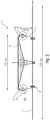
- the Fig. 1 shows a three-dimensional representation of an antenna device 1 with a carrier element 2 and a radiator element 4.
- a ground surface 10 is also located on the carrier element 2 here. It can be seen that the radiator element 4 has a square outer contour and descends in a funnel shape. The radiator element 4 is at a distance from the carrier element 2 and is held or supported here by the four coupling points or by the four wing elements 6.
- the Indian Fig. 1 circled area is in the Fig. 2 shown larger.
- the four wing elements 6 can be seen, which are located on the sides 40 of the here rectangular radiator element 4 and have coupling points 5 for the capacitive coupling at their free ends 60.
- Four web elements 7 extend from the carrier element 2 at the four feed points 8. The web elements 7 and the wing elements 6 meet at the coupling points 5 and cause the capacitive coupling there.
- the radiator element 4 lowers centrally towards the carrier element 2. It can also be seen that the wing elements 6 and thereby the coupling points 5 are located on the sides 40 of the radiator element 4, which is square here. Like the radiator element 4, the wing elements 6 are designed here as metal sheets and are in particular galvanically coupled to the radiator element 4. Between the wing elements 6 and the web elements 7 there is in each case an intermediate medium 9 in the coupling area 5, which is designed here as a dielectric and therefore also Has effects on the capacitive coupling and which enables the radiator element 4 to be fixed with a defined distance between the wing element 6 and the web element 7. Furthermore, the web elements 7 are galvanically coupled to the conductor structure on the carrier element 2 at the feed points 8. The wing elements 6 and the radiator element 4 or its outer border form an angle 14, which here is a 90 ° angle. The wing elements 6 face the carrier element 2 here and also face away from the top of the radiator element 4.
- the conductor structure 3 in the form of conductor tracks on the carrier element 2 shows Fig. 4 .
- the conductor structure 3 is located below the radiator element 4 and on the opposite side of the ground plane 10, i.e. below the carrier element 2.
- the earth plane 10 is below and the conductor structure 3 is above the carrier element 2.
- the ground plane 10 or the conductor structure 3 within any number of layered carrier elements 2.
- the web elements 7 or possibly existing elements that connect the conductor structure 3 to the web elements 7 therefore protrude through the carrier element 2 depending on the configuration.
- FIGs. 1 to 4 thus show the novel capacitive coupling of the radiator element 4 using the example of a patch with four feed points.
- the radiator element 4 can be easily adapted to a desired impedance, often 50 ohms, without a large ground plane 10 or without a reflector.
- the coupling points 5 are located on the sides 40 of the radiator element 4.
- the wings or wing elements 6) are attached to the sides of the radiator element 4 and are bent downwards.
- Four webs protrude from the carrier board 2 - one web (or web element 7) per feed point 8 - and couple capacitively with the wings 7 via an intermediate medium 9.
- This allows the width of the coupling gap between web 7 and wing 6 to be reduced and also enables a defined distance between web 7 and wing 6.
- an air gap can also be provided.
- the radiator element 4 or the wing elements 6 can also be attached to the webs 7, for. B. screwed, plugged, glued or soldered to the intermediate medium between web 7 and wing 6. Almost any impedance matching is possible due to the width, height and spacing of the coupling point 5 possible, which significantly simplifies the development of the antenna element 1, since no lossy matching network is required.
- the shape of the radiator element 4 and the capacitive coupling points 5 generate high field strengths at the coupling points 5, in which the majority of the energy fed in is concentrated. This imposes a wide electrical aperture on the radiator 4, as a result of which the lateral dimensions of the radiator 4 can be significantly reduced.
- Fig. 5 shows examples of some variants.
- the radiator element 4 can be shaped or configured differently.
- Fig. 6 shows examples of some variants.
- an n-cornered radiator element 4 is shown, the outer contour of which is formed by the n-corner.
- n is a natural number greater than three.
- the Fig. 7 shows variants with a monopole as a design of the radiator element 4. Furthermore, different variants for the coupling with web elements 7 are shown. In some of the configurations there are no wing elements, so that the radiator element 4 has the at least one coupling point directly on one side 40.
- the variants of the Fig. 7 a) to e) and l ) only have the radiator element 4 and the bar element 7.
- the variants of the Fig. 7 f) to k) have the radiator element 4, at least one wing element 5 and at least one web element 7.
- the radiator elements 4 are surface radiators, e.g. B. in the form of wide sheet metal elements. This shows the Fig. 7 I) who have a 90 ° rotated view of the design of the Fig. 7 b) allowed.
- the side 40 of the radiator element 4 is given here by the base area.
- the web element 7, designed here as a strip, is located on this side 40 through the coupling point 5 in a capacitive connection with the radiator element 4.
- the webs 7 can also be designed differently. These can vary in width, height, thickness and shape. They can also be straight or angled. In addition to air, an intermediate medium 9, e.g. B. dielectrics, ferrites, ferroelectrics and others.
- the fastening of the web elements 7 on the feeder board as an example for the carrier element 2 can be implemented differently like the fastening of the radiator element 4 to the web elements 7, e.g. B. screwed, plugged, glued or soldered.
- FIGS 9 and 10 show two further embodiments with four points for capacitive coupling between the conductor structure on the carrier element 2 and the radiator element 4.
- the wing elements 6 are located on the sides of the n-angular radiator element 4 and are bent in the direction of the carrier element 2.
- a capacitive coupling - here in particular via an air gap - between the web element 7 and the wing element 6, so that the capacitive coupling point 5 is also located between the two.
- the wing elements 6 can also be seen here as sheet metal strips that are attached to the sides of the radiator element 4 and are bent downwards. It can also be seen that, via the configurations of wing elements 6 and web elements 7, the distance between the radiator element 6 and the carrier element 2 or z. B. a ground plane on the carrier element 2 are adjustable.
- the at least one radiator element 4 is made from sheet metal, the wing elements 6 and the web elements 7 also being made from sheet metal.
- FIGS. 11 to 14 show a further embodiment of the antenna device 1 with two radiator elements 4, 4 '.
- This is, for example, a "stacked patch", e.g. B. for dual-band design or extended broadband design.
- the Fig. 11 shows the two differently configured radiator elements 4, 4 ′, both of which are spaced apart from the carrier element 2.
- the radiator element 4 located higher also the first radiator element
- the second radiator element 4 ' is located within the recess 21 and closer to the carrier element 2.
- the second radiator element 4' in the illustrated embodiment is also designed to be square.
- Both radiator elements 4, 4 ' are designed flat here and are here essentially parallel to the carrier element 2.
- the conductor structure 3 can be seen in the form of conductor tracks on the carrier element 2 with the four feed points 8, each of which is connected to a web element 7. This is done here to match the four coupling points 5 on the wing elements 6 on the four outer sides 40 of the upper radiator element 4.
- the Fig. 12 shows the different configuration of the two radiator elements 4, 4 'and their arrangement with respect to one another. It can also be seen that the wing elements 6 are located on the sides 40 of the upper or first square radiator element 4 and protrude from there in the direction of the carrier element 2. The capacitive coupling points 5 are therefore also on the sides. The flat course of the wing elements can also be seen, which extend from the sides of the upper radiator element 4 and are angled here in the direction of the carrier element 2.
- the Fig. 13 shows the enlarged section of the part of the antenna device 1 of FIG Fig. 12 .
- Tongue elements 15 protrude from the coupling points 5 to the radiator element 4 'located further in the direction of the carrier element 2 and therefore also generate an electrical - here in particular capacitive - coupling to this - second - radiator element 4'.
- the two radiating elements 4, 4 ′ are capacitively coupled to one another and one of the two radiating elements 4 is capacitively coupled to the conductor structure 3 via the wing elements 6.
- the cut of the Fig. 14 shows once again that the upper - first - radiator element 4 rests on the carrier element 2 via the connection of laterally located wing elements 6 and web elements 7 and is capacitively coupled to the feed points 8 via the coupling points 5.
- a dielectric is located between the web elements 7 and the wing elements 6 as an intermediate medium 9.
- the tongue elements 15 run in the direction of the lower - second - radiator element 4 ′, which also effect electrical and, here, capacitive contact.
- the carrier element 2 has a width of 175 mm and the upper radiator element 4 has a side length of 75 mm.
- the outer contour - here in particular square - of the upper radiator element 4 is located approximately 25 mm above the carrier element 2.
- UHF RFID antennas for use in logistics, production or automation offer a technical field of application. These include, for example, gate passages with bulk reading (recording of many transponders in a short time), automated inventory or personal checks (e.g. healthcare).
- Another possible application is mobile terminals for satellite or terrestrial mobile communication. Further applications are in the automotive sector or in the area of networking vehicles or road users (so-called Car2X).
Landscapes
- Physics & Mathematics (AREA)
- Electromagnetism (AREA)
- Details Of Aerials (AREA)
- Waveguide Aerials (AREA)
- Aerials With Secondary Devices (AREA)
- Variable-Direction Aerials And Aerial Arrays (AREA)
Claims (14)
- Dispositif d'antenne (1)
avec un élément de rayonnement (4) destiné à émettre et/ou recevoir des signaux électromagnétiques,
dans lequel l'élément de rayonnement (4) présente au moins un point de couplage (5),
dans lequel le point de couplage (5) est connecté à un côté (40) de l'élément de rayonnement (4), et
dans lequel le point de couplage (5) est conçu pour le couplage et/ou découplage capacitif de signaux électromagnétiques, dans lequel le dispositif d'antenne (1) présente une structure conductrice (3) destinée à conduire des signaux électromagnétiques, et
dans lequel la structure conductrice (3) et l'élément de rayonnement (4) sont couplés de manière capacitive l'un à l'autre par l'intermédiaire du point de couplage (5),
dans lequel l'élément de rayonnement (4) présente au moins un élément d'aile (6),
dans lequel l'élément de rayonnement (4) et l'élément d'aile (6) sont couplés de manière galvanique l'un à l'autre,
dans lequel l'élément d'aile (6) est disposé sur le côté (40) de l'élément de rayonnement (4),
dans lequel l'élément de rayonnement (4) et l'élément d'aile (6) forment un angle (14) entre eux,
dans lequel l'élément d'aile (6) présente le point de couplage (5), dans lequel le dispositif d'antenne (1) présente au moins un élément de bretelle (7),
dans lequel l'élément de bretelle (7) est couplé de manière galvanique ou de manière capacitive à un point d'alimentation (8) de la structure conductrice (3), et
dans lequel l'élément de bretelle (7) et l'élément de rayonnement (4) sont couplés de manière capacitive l'un à l'autre par l'intermédiaire du point de couplage (5),
dans lequel le dispositif d'antenne (1) présente un élément de support (2),
dans lequel l'élément d'aile (6) forme un angle en direction de l'élément de support (2) par rapport à l'élément de rayonnement (4), et le point de couplage (5) se situe à une extrémité libre (60) de l'élément d'aile (6),
caractérisé par le fait que l'élément de rayonnement (4) est conçu sous forme d'émetteur de surface. - Dispositif d'antenne (1) selon la revendication 1,
dans lequel est présent, à l'endroit du point de couplage (5), un milieu intermédiaire (9) et dans lequel le couplage capacitif a lieu par l'intermédiaire du milieu intermédiaire (9). - Dispositif d'antenne (1) selon la revendication 1 ou 2,
dans lequel l'élément de rayonnement (4) est fixé à distance de l'élément de support (2). - Dispositif d'antenne (1) selon la revendication 1,
dans lequel l'élément de rayonnement (4) est conçu sous forme d'émetteur de surface avec un contour extérieur en forme de polygone à n côtés; et
où n est un nombre naturel supérieur ou égal à trois. - Dispositif d'antenne (1) selon la revendication 1 ou 4,
dans lequel l'élément de rayonnement (4) est conçu sous forme d'émetteur de surface en forme d'entonnoir avec une dépression centrale. - Dispositif d'antenne (1) selon la revendication 4,
dans lequel le point de couplage (5) est disposé au centre dans la zone d'un côté du polygone à n côtés de l'élément de rayonnement (4). - Dispositif d'antenne (1) selon l'une des revendications 4 à 6,
dans lequel l'élément de rayonnement (4) est conçu sous forme de tôle. - Dispositif d'antenne (1) selon l'une des revendications 1 à 7,
dans lequel l'élément de rayonnement (4) présente des points de couplage (5) sur plusieurs côtés (40); et
dans lequel l'élément de rayonnement (4) est couplé de manière capacitive, par l'intermédiaire d'au moins un point de couplage (5), à la structure conductrice (3). - Dispositif d'antenne (1) selon la revendication 8,
dans lequel l'élément de rayonnement (4) est connecté, par l'intermédiaire d'au moins un point de couplage (5), à un circuit ouvert (12), de sorte que soit présente une extrémité ouverte. - Dispositif d'antenne (1) selon la revendication 8,
dans lequel l'élément de rayonnement (4) est connecté, par l'intermédiaire d'au moins un point de couplage (5), à un courtcircuit (13). - Dispositif d'antenne (1) selon l'une des revendications 1 à 10,
dans lequel le dispositif d'antenne (1) présente au moins deux éléments de rayonnement (4, 4'). - Dispositif d'antenne (1) selon la revendication 11,
dans lequel les deux éléments de rayonnement (4, 4') sont couplés l'un à l'autre, en particulier de manière capacitive ou galvanique. - Dispositif d'antenne (1) selon la revendication 11 ou 12,
dans lequel les deux éléments de rayonnement (4, 4') présentent des distances différentes par rapport à l'élément de support (2). - Dispositif d'antenne (1) selon l'une des revendications 11 à 13,
dans lequel un élément de rayonnement (4) parmi les deux éléments de rayonnement (4, 4') présente un évidement (21) et dans lequel un autre élément de rayonnement (4') parmi les deux éléments de rayonnement (4, 4') est disposé dans la zone de l'évidement (21).
Applications Claiming Priority (3)
| Application Number | Priority Date | Filing Date | Title |
|---|---|---|---|
| DE102016205842 | 2016-04-07 | ||
| DE102016207434.2A DE102016207434B4 (de) | 2016-04-07 | 2016-04-29 | Antennenvorrichtung |
| PCT/EP2017/058278 WO2017174736A1 (fr) | 2016-04-07 | 2017-04-06 | Dispositif d'antenne |
Publications (2)
| Publication Number | Publication Date |
|---|---|
| EP3440738A1 EP3440738A1 (fr) | 2019-02-13 |
| EP3440738B1 true EP3440738B1 (fr) | 2021-04-21 |
Family
ID=59930125
Family Applications (1)
| Application Number | Title | Priority Date | Filing Date |
|---|---|---|---|
| EP17716202.1A Active EP3440738B1 (fr) | 2016-04-07 | 2017-04-06 | Dispositif d'antenne |
Country Status (6)
| Country | Link |
|---|---|
| US (1) | US11223131B2 (fr) |
| EP (1) | EP3440738B1 (fr) |
| JP (1) | JP6795614B2 (fr) |
| CN (1) | CN109219906B (fr) |
| DE (1) | DE102016207434B4 (fr) |
| WO (1) | WO2017174736A1 (fr) |
Families Citing this family (14)
| Publication number | Priority date | Publication date | Assignee | Title |
|---|---|---|---|---|
| KR101609665B1 (ko) * | 2014-11-11 | 2016-04-06 | 주식회사 케이엠더블유 | 이동통신 기지국 안테나 |
| DE102018201575B3 (de) * | 2018-02-01 | 2019-06-13 | Fraunhofer-Gesellschaft zur Förderung der angewandten Forschung e.V. | Antennenvorrichtung |
| EP3671951A1 (fr) * | 2018-12-21 | 2020-06-24 | FRAUNHOFER-GESELLSCHAFT zur Förderung der angewandten Forschung e.V. | Dispositif antenne |
| CN113994542A (zh) * | 2019-05-24 | 2022-01-28 | 康普技术有限责任公司 | 其中具有支持大扫描角辐射的贴片型天线阵列的无线通信系统 |
| KR102765419B1 (ko) * | 2020-06-08 | 2025-02-11 | 삼성전자주식회사 | 안테나 구조 및 이를 포함하는 전자 장치 |
| CN111786078B (zh) * | 2020-08-04 | 2021-06-25 | 大连海事大学 | 一种圆极化波束宽的宽带射频识别读写器天线 |
| KR102928268B1 (ko) * | 2020-09-21 | 2026-02-19 | 삼성전자주식회사 | 안테나 구조 및 이를 포함하는 전자 장치 |
| CN113422200B (zh) * | 2021-07-05 | 2023-11-10 | 江苏方天电力技术有限公司 | 一种背反射多频点镂空内置天线及其设计方法 |
| CN114400442B (zh) * | 2022-03-25 | 2022-05-31 | 成都天锐星通科技有限公司 | 双圆极化天线单元和双圆极化阵面天线 |
| CN115101930B (zh) * | 2022-07-15 | 2022-11-15 | 广东工业大学 | 边缘加载谐振枝节的双频卫星导航天线 |
| DE102022132788A1 (de) * | 2022-12-09 | 2024-06-20 | Fuba Automotive Electronics Gmbh | Satellitenantenne |
| US12476364B2 (en) * | 2023-04-24 | 2025-11-18 | GM Global Technology Operations LLC | Ultra wideband antenna with partial cap |
| US12531351B2 (en) | 2023-09-27 | 2026-01-20 | GM Global Technology Operations LLC | Ultra wideband antenna including radio frequency balun |
| US12597708B2 (en) | 2023-09-27 | 2026-04-07 | GM Global Technology Operations LLC | Ultra wideband antenna including radio frequency balun |
Citations (1)
| Publication number | Priority date | Publication date | Assignee | Title |
|---|---|---|---|---|
| US20030174098A1 (en) * | 2002-01-29 | 2003-09-18 | Mitsmi Electric Co., Ltd. | Four-point feeding loop antenna capable of easily obtaining an impednace match |
Family Cites Families (10)
| Publication number | Priority date | Publication date | Assignee | Title |
|---|---|---|---|---|
| EP2073309B1 (fr) * | 2007-12-21 | 2015-02-25 | Alcatel Lucent | Élément de rayonnement à double polarisation pour antennes de station de base cellulaire |
| DE102010035934A1 (de) * | 2010-08-31 | 2012-03-01 | Heinz Lindenmeier | Empfangsantenne für zirkular polarisierte Satellitenfunksignale |
| US9647328B2 (en) | 2011-11-04 | 2017-05-09 | Kathrein-Werke Kg | Patch radiator |
| US8890766B2 (en) * | 2011-12-01 | 2014-11-18 | Sony Corporation | Low profile multi-band antennas and related wireless communications devices |
| DE102012101443B4 (de) * | 2012-02-23 | 2017-02-09 | Turck Holding Gmbh | Planare Antennenanordnung |
| CN202797284U (zh) * | 2012-10-10 | 2013-03-13 | 华为技术有限公司 | 一种馈电网络、天线及双极化天线阵列馈电电路 |
| US9246222B2 (en) * | 2013-03-15 | 2016-01-26 | Tyco Electronics Corporation | Compact wideband patch antenna |
| US9634396B2 (en) * | 2013-07-09 | 2017-04-25 | Galtronics Corporation Ltd. | Extremely low-profile antenna |
| US9711853B2 (en) * | 2013-08-07 | 2017-07-18 | Huawei Technologies Co., Ltd. | Broadband low-beam-coupling dual-beam phased array |
| EP3387705B1 (fr) * | 2016-04-26 | 2022-06-22 | Huawei Technologies Co., Ltd. | Agencement d'antenne |
-
2016
- 2016-04-29 DE DE102016207434.2A patent/DE102016207434B4/de active Active
-
2017
- 2017-04-06 EP EP17716202.1A patent/EP3440738B1/fr active Active
- 2017-04-06 WO PCT/EP2017/058278 patent/WO2017174736A1/fr not_active Ceased
- 2017-04-06 CN CN201780034015.1A patent/CN109219906B/zh active Active
- 2017-04-06 JP JP2018552833A patent/JP6795614B2/ja active Active
-
2018
- 2018-10-04 US US16/151,674 patent/US11223131B2/en active Active
Patent Citations (1)
| Publication number | Priority date | Publication date | Assignee | Title |
|---|---|---|---|---|
| US20030174098A1 (en) * | 2002-01-29 | 2003-09-18 | Mitsmi Electric Co., Ltd. | Four-point feeding loop antenna capable of easily obtaining an impednace match |
Also Published As
| Publication number | Publication date |
|---|---|
| JP2019514285A (ja) | 2019-05-30 |
| JP6795614B2 (ja) | 2020-12-02 |
| DE102016207434A1 (de) | 2017-10-12 |
| US11223131B2 (en) | 2022-01-11 |
| CN109219906A (zh) | 2019-01-15 |
| DE102016207434B4 (de) | 2017-11-23 |
| US20190044238A1 (en) | 2019-02-07 |
| CN109219906B (zh) | 2020-12-01 |
| EP3440738A1 (fr) | 2019-02-13 |
| WO2017174736A1 (fr) | 2017-10-12 |
Similar Documents
| Publication | Publication Date | Title |
|---|---|---|
| EP3440738B1 (fr) | Dispositif d'antenne | |
| EP1842262B1 (fr) | Antenne a orifice couple | |
| EP3411921B1 (fr) | Antenne à double polarisation | |
| DE102005010894B4 (de) | Planare Mehrbandantenne | |
| DE102017103161B4 (de) | Antennenvorrichtung und Antennenarray | |
| EP2664025B1 (fr) | Antenne de réception multibande pour la réception combinée de signaux satellites et de signaux radiophoniques à émission terrestre | |
| EP2721690B1 (fr) | Élément rayonnant "patch" | |
| DE102008023030B4 (de) | Radarantennenanordnung | |
| EP2135324B1 (fr) | Dispositif d'antenne pour émettre et recevoir des signaux électromagnétiques | |
| EP2256673B1 (fr) | Transpondeur RFID destiné au montage sur métal et son procédé de fabrication | |
| DE60213902T2 (de) | M-förmige Antenne | |
| DE102011076209B4 (de) | Antenne | |
| DE602005002330T2 (de) | Logarithmisch periodische Mikrostreifengruppenantenne mit geerdetem halbkoplanaren Übergang von Wellenleiter auf Mikrostreifenleitung | |
| DE102015007503A1 (de) | Dipolförmige Strahleranordnung | |
| DE102014018573B4 (de) | Antennenanordnung mit planarer geschlitzter Patchantenne hoher Bandbreite | |
| DE112021006900B4 (de) | Antennenvorrichtung | |
| DE102012016627A1 (de) | Patch-Strahler | |
| DE102012101443B4 (de) | Planare Antennenanordnung | |
| DE102004050598A1 (de) | Dualband-Antenne für zirkulare Polarisation | |
| WO2019158543A1 (fr) | Antenne de communication avec un transpondeur | |
| EP3827478B1 (fr) | Antenne à carte de circuit imprimé | |
| EP3349303B1 (fr) | Dispositif d'antenne combine | |
| EP3707775B1 (fr) | Dispositif de couplage et découplage entre un support de circuit et un guide d'onde | |
| EP4525210B1 (fr) | Antenne satellite |
Legal Events
| Date | Code | Title | Description |
|---|---|---|---|
| STAA | Information on the status of an ep patent application or granted ep patent |
Free format text: STATUS: UNKNOWN |
|
| STAA | Information on the status of an ep patent application or granted ep patent |
Free format text: STATUS: THE INTERNATIONAL PUBLICATION HAS BEEN MADE |
|
| PUAI | Public reference made under article 153(3) epc to a published international application that has entered the european phase |
Free format text: ORIGINAL CODE: 0009012 |
|
| STAA | Information on the status of an ep patent application or granted ep patent |
Free format text: STATUS: REQUEST FOR EXAMINATION WAS MADE |
|
| 17P | Request for examination filed |
Effective date: 20181004 |
|
| AK | Designated contracting states |
Kind code of ref document: A1 Designated state(s): AL AT BE BG CH CY CZ DE DK EE ES FI FR GB GR HR HU IE IS IT LI LT LU LV MC MK MT NL NO PL PT RO RS SE SI SK SM TR |
|
| AX | Request for extension of the european patent |
Extension state: BA ME |
|
| DAV | Request for validation of the european patent (deleted) | ||
| DAX | Request for extension of the european patent (deleted) | ||
| GRAP | Despatch of communication of intention to grant a patent |
Free format text: ORIGINAL CODE: EPIDOSNIGR1 |
|
| STAA | Information on the status of an ep patent application or granted ep patent |
Free format text: STATUS: GRANT OF PATENT IS INTENDED |
|
| INTG | Intention to grant announced |
Effective date: 20201104 |
|
| GRAS | Grant fee paid |
Free format text: ORIGINAL CODE: EPIDOSNIGR3 |
|
| GRAA | (expected) grant |
Free format text: ORIGINAL CODE: 0009210 |
|
| STAA | Information on the status of an ep patent application or granted ep patent |
Free format text: STATUS: THE PATENT HAS BEEN GRANTED |
|
| AK | Designated contracting states |
Kind code of ref document: B1 Designated state(s): AL AT BE BG CH CY CZ DE DK EE ES FI FR GB GR HR HU IE IS IT LI LT LU LV MC MK MT NL NO PL PT RO RS SE SI SK SM TR |
|
| REG | Reference to a national code |
Ref country code: GB Ref legal event code: FG4D Free format text: NOT ENGLISH |
|
| REG | Reference to a national code |
Ref country code: CH Ref legal event code: EP |
|
| REG | Reference to a national code |
Ref country code: DE Ref legal event code: R096 Ref document number: 502017010138 Country of ref document: DE Ref country code: IE Ref legal event code: FG4D Free format text: LANGUAGE OF EP DOCUMENT: GERMAN |
|
| REG | Reference to a national code |
Ref country code: AT Ref legal event code: REF Ref document number: 1385614 Country of ref document: AT Kind code of ref document: T Effective date: 20210515 |
|
| REG | Reference to a national code |
Ref country code: LT Ref legal event code: MG9D |
|
| REG | Reference to a national code |
Ref country code: NL Ref legal event code: MP Effective date: 20210421 |
|
| PG25 | Lapsed in a contracting state [announced via postgrant information from national office to epo] |
Ref country code: HR Free format text: LAPSE BECAUSE OF FAILURE TO SUBMIT A TRANSLATION OF THE DESCRIPTION OR TO PAY THE FEE WITHIN THE PRESCRIBED TIME-LIMIT Effective date: 20210421 Ref country code: BG Free format text: LAPSE BECAUSE OF FAILURE TO SUBMIT A TRANSLATION OF THE DESCRIPTION OR TO PAY THE FEE WITHIN THE PRESCRIBED TIME-LIMIT Effective date: 20210721 Ref country code: NL Free format text: LAPSE BECAUSE OF FAILURE TO SUBMIT A TRANSLATION OF THE DESCRIPTION OR TO PAY THE FEE WITHIN THE PRESCRIBED TIME-LIMIT Effective date: 20210421 Ref country code: LT Free format text: LAPSE BECAUSE OF FAILURE TO SUBMIT A TRANSLATION OF THE DESCRIPTION OR TO PAY THE FEE WITHIN THE PRESCRIBED TIME-LIMIT Effective date: 20210421 Ref country code: FI Free format text: LAPSE BECAUSE OF FAILURE TO SUBMIT A TRANSLATION OF THE DESCRIPTION OR TO PAY THE FEE WITHIN THE PRESCRIBED TIME-LIMIT Effective date: 20210421 |
|
| PG25 | Lapsed in a contracting state [announced via postgrant information from national office to epo] |
Ref country code: LV Free format text: LAPSE BECAUSE OF FAILURE TO SUBMIT A TRANSLATION OF THE DESCRIPTION OR TO PAY THE FEE WITHIN THE PRESCRIBED TIME-LIMIT Effective date: 20210421 Ref country code: GR Free format text: LAPSE BECAUSE OF FAILURE TO SUBMIT A TRANSLATION OF THE DESCRIPTION OR TO PAY THE FEE WITHIN THE PRESCRIBED TIME-LIMIT Effective date: 20210722 Ref country code: IS Free format text: LAPSE BECAUSE OF FAILURE TO SUBMIT A TRANSLATION OF THE DESCRIPTION OR TO PAY THE FEE WITHIN THE PRESCRIBED TIME-LIMIT Effective date: 20210821 Ref country code: PT Free format text: LAPSE BECAUSE OF FAILURE TO SUBMIT A TRANSLATION OF THE DESCRIPTION OR TO PAY THE FEE WITHIN THE PRESCRIBED TIME-LIMIT Effective date: 20210823 Ref country code: NO Free format text: LAPSE BECAUSE OF FAILURE TO SUBMIT A TRANSLATION OF THE DESCRIPTION OR TO PAY THE FEE WITHIN THE PRESCRIBED TIME-LIMIT Effective date: 20210721 Ref country code: PL Free format text: LAPSE BECAUSE OF FAILURE TO SUBMIT A TRANSLATION OF THE DESCRIPTION OR TO PAY THE FEE WITHIN THE PRESCRIBED TIME-LIMIT Effective date: 20210421 Ref country code: SE Free format text: LAPSE BECAUSE OF FAILURE TO SUBMIT A TRANSLATION OF THE DESCRIPTION OR TO PAY THE FEE WITHIN THE PRESCRIBED TIME-LIMIT Effective date: 20210421 Ref country code: RS Free format text: LAPSE BECAUSE OF FAILURE TO SUBMIT A TRANSLATION OF THE DESCRIPTION OR TO PAY THE FEE WITHIN THE PRESCRIBED TIME-LIMIT Effective date: 20210421 |
|
| REG | Reference to a national code |
Ref country code: DE Ref legal event code: R097 Ref document number: 502017010138 Country of ref document: DE |
|
| PG25 | Lapsed in a contracting state [announced via postgrant information from national office to epo] |
Ref country code: SM Free format text: LAPSE BECAUSE OF FAILURE TO SUBMIT A TRANSLATION OF THE DESCRIPTION OR TO PAY THE FEE WITHIN THE PRESCRIBED TIME-LIMIT Effective date: 20210421 Ref country code: SK Free format text: LAPSE BECAUSE OF FAILURE TO SUBMIT A TRANSLATION OF THE DESCRIPTION OR TO PAY THE FEE WITHIN THE PRESCRIBED TIME-LIMIT Effective date: 20210421 Ref country code: RO Free format text: LAPSE BECAUSE OF FAILURE TO SUBMIT A TRANSLATION OF THE DESCRIPTION OR TO PAY THE FEE WITHIN THE PRESCRIBED TIME-LIMIT Effective date: 20210421 Ref country code: ES Free format text: LAPSE BECAUSE OF FAILURE TO SUBMIT A TRANSLATION OF THE DESCRIPTION OR TO PAY THE FEE WITHIN THE PRESCRIBED TIME-LIMIT Effective date: 20210421 Ref country code: EE Free format text: LAPSE BECAUSE OF FAILURE TO SUBMIT A TRANSLATION OF THE DESCRIPTION OR TO PAY THE FEE WITHIN THE PRESCRIBED TIME-LIMIT Effective date: 20210421 Ref country code: DK Free format text: LAPSE BECAUSE OF FAILURE TO SUBMIT A TRANSLATION OF THE DESCRIPTION OR TO PAY THE FEE WITHIN THE PRESCRIBED TIME-LIMIT Effective date: 20210421 Ref country code: CZ Free format text: LAPSE BECAUSE OF FAILURE TO SUBMIT A TRANSLATION OF THE DESCRIPTION OR TO PAY THE FEE WITHIN THE PRESCRIBED TIME-LIMIT Effective date: 20210421 |
|
| PLBE | No opposition filed within time limit |
Free format text: ORIGINAL CODE: 0009261 |
|
| STAA | Information on the status of an ep patent application or granted ep patent |
Free format text: STATUS: NO OPPOSITION FILED WITHIN TIME LIMIT |
|
| 26N | No opposition filed |
Effective date: 20220124 |
|
| PG25 | Lapsed in a contracting state [announced via postgrant information from national office to epo] |
Ref country code: IS Free format text: LAPSE BECAUSE OF FAILURE TO SUBMIT A TRANSLATION OF THE DESCRIPTION OR TO PAY THE FEE WITHIN THE PRESCRIBED TIME-LIMIT Effective date: 20210821 Ref country code: AL Free format text: LAPSE BECAUSE OF FAILURE TO SUBMIT A TRANSLATION OF THE DESCRIPTION OR TO PAY THE FEE WITHIN THE PRESCRIBED TIME-LIMIT Effective date: 20210421 |
|
| PG25 | Lapsed in a contracting state [announced via postgrant information from national office to epo] |
Ref country code: IT Free format text: LAPSE BECAUSE OF FAILURE TO SUBMIT A TRANSLATION OF THE DESCRIPTION OR TO PAY THE FEE WITHIN THE PRESCRIBED TIME-LIMIT Effective date: 20210421 |
|
| REG | Reference to a national code |
Ref country code: CH Ref legal event code: PL |
|
| REG | Reference to a national code |
Ref country code: BE Ref legal event code: MM Effective date: 20220430 |
|
| PG25 | Lapsed in a contracting state [announced via postgrant information from national office to epo] |
Ref country code: MC Free format text: LAPSE BECAUSE OF FAILURE TO SUBMIT A TRANSLATION OF THE DESCRIPTION OR TO PAY THE FEE WITHIN THE PRESCRIBED TIME-LIMIT Effective date: 20210421 Ref country code: LU Free format text: LAPSE BECAUSE OF NON-PAYMENT OF DUE FEES Effective date: 20220406 Ref country code: LI Free format text: LAPSE BECAUSE OF NON-PAYMENT OF DUE FEES Effective date: 20220430 Ref country code: CH Free format text: LAPSE BECAUSE OF NON-PAYMENT OF DUE FEES Effective date: 20220430 |
|
| PG25 | Lapsed in a contracting state [announced via postgrant information from national office to epo] |
Ref country code: BE Free format text: LAPSE BECAUSE OF NON-PAYMENT OF DUE FEES Effective date: 20220430 |
|
| PG25 | Lapsed in a contracting state [announced via postgrant information from national office to epo] |
Ref country code: IE Free format text: LAPSE BECAUSE OF NON-PAYMENT OF DUE FEES Effective date: 20220406 |
|
| REG | Reference to a national code |
Ref country code: AT Ref legal event code: MM01 Ref document number: 1385614 Country of ref document: AT Kind code of ref document: T Effective date: 20220406 |
|
| P01 | Opt-out of the competence of the unified patent court (upc) registered |
Effective date: 20230524 |
|
| PG25 | Lapsed in a contracting state [announced via postgrant information from national office to epo] |
Ref country code: AT Free format text: LAPSE BECAUSE OF NON-PAYMENT OF DUE FEES Effective date: 20220406 |
|
| PG25 | Lapsed in a contracting state [announced via postgrant information from national office to epo] |
Ref country code: HU Free format text: LAPSE BECAUSE OF FAILURE TO SUBMIT A TRANSLATION OF THE DESCRIPTION OR TO PAY THE FEE WITHIN THE PRESCRIBED TIME-LIMIT; INVALID AB INITIO Effective date: 20170406 |
|
| PG25 | Lapsed in a contracting state [announced via postgrant information from national office to epo] |
Ref country code: MK Free format text: LAPSE BECAUSE OF FAILURE TO SUBMIT A TRANSLATION OF THE DESCRIPTION OR TO PAY THE FEE WITHIN THE PRESCRIBED TIME-LIMIT Effective date: 20210421 Ref country code: CY Free format text: LAPSE BECAUSE OF FAILURE TO SUBMIT A TRANSLATION OF THE DESCRIPTION OR TO PAY THE FEE WITHIN THE PRESCRIBED TIME-LIMIT Effective date: 20210421 |
|
| PG25 | Lapsed in a contracting state [announced via postgrant information from national office to epo] |
Ref country code: MT Free format text: LAPSE BECAUSE OF FAILURE TO SUBMIT A TRANSLATION OF THE DESCRIPTION OR TO PAY THE FEE WITHIN THE PRESCRIBED TIME-LIMIT Effective date: 20210421 |
|
| PGFP | Annual fee paid to national office [announced via postgrant information from national office to epo] |
Ref country code: DE Payment date: 20250417 Year of fee payment: 9 |
|
| PGFP | Annual fee paid to national office [announced via postgrant information from national office to epo] |
Ref country code: FR Payment date: 20250422 Year of fee payment: 9 |
|
| PG25 | Lapsed in a contracting state [announced via postgrant information from national office to epo] |
Ref country code: TR Free format text: LAPSE BECAUSE OF FAILURE TO SUBMIT A TRANSLATION OF THE DESCRIPTION OR TO PAY THE FEE WITHIN THE PRESCRIBED TIME-LIMIT Effective date: 20210421 |
|
| PGFP | Annual fee paid to national office [announced via postgrant information from national office to epo] |
Ref country code: GB Payment date: 20260324 Year of fee payment: 10 |