EP3441817A1 - Commutateur optique - Google Patents
Commutateur optique Download PDFInfo
- Publication number
- EP3441817A1 EP3441817A1 EP16901003.0A EP16901003A EP3441817A1 EP 3441817 A1 EP3441817 A1 EP 3441817A1 EP 16901003 A EP16901003 A EP 16901003A EP 3441817 A1 EP3441817 A1 EP 3441817A1
- Authority
- EP
- European Patent Office
- Prior art keywords
- waveguide
- optical sub
- optical
- junction
- sub
- Prior art date
- Legal status (The legal status is an assumption and is not a legal conclusion. Google has not performed a legal analysis and makes no representation as to the accuracy of the status listed.)
- Granted
Links
Images



Classifications
-
- G—PHYSICS
- G02—OPTICS
- G02B—OPTICAL ELEMENTS, SYSTEMS OR APPARATUS
- G02B6/00—Light guides; Structural details of arrangements comprising light guides and other optical elements, e.g. couplings
- G02B6/10—Light guides; Structural details of arrangements comprising light guides and other optical elements, e.g. couplings of the optical waveguide type
- G02B6/12—Light guides; Structural details of arrangements comprising light guides and other optical elements, e.g. couplings of the optical waveguide type of the integrated circuit kind
- G02B6/122—Basic optical elements, e.g. light-guiding paths
-
- G—PHYSICS
- G02—OPTICS
- G02F—OPTICAL DEVICES OR ARRANGEMENTS FOR THE CONTROL OF LIGHT BY MODIFICATION OF THE OPTICAL PROPERTIES OF THE MEDIA OF THE ELEMENTS INVOLVED THEREIN; NON-LINEAR OPTICS; FREQUENCY-CHANGING OF LIGHT; OPTICAL LOGIC ELEMENTS; OPTICAL ANALOGUE/DIGITAL CONVERTERS
- G02F1/00—Devices or arrangements for the control of the intensity, colour, phase, polarisation or direction of light arriving from an independent light source, e.g. switching, gating or modulating; Non-linear optics
- G02F1/29—Devices or arrangements for the control of the intensity, colour, phase, polarisation or direction of light arriving from an independent light source, e.g. switching, gating or modulating; Non-linear optics for the control of the position or the direction of light beams, i.e. deflection
- G02F1/31—Digital deflection, i.e. optical switching
- G02F1/313—Digital deflection, i.e. optical switching in an optical waveguide structure
- G02F1/3137—Digital deflection, i.e. optical switching in an optical waveguide structure with intersecting or branching waveguides, e.g. X-switches and Y-junctions
- G02F1/3138—Digital deflection, i.e. optical switching in an optical waveguide structure with intersecting or branching waveguides, e.g. X-switches and Y-junctions the optical waveguides being made of semiconducting materials
-
- G—PHYSICS
- G02—OPTICS
- G02B—OPTICAL ELEMENTS, SYSTEMS OR APPARATUS
- G02B6/00—Light guides; Structural details of arrangements comprising light guides and other optical elements, e.g. couplings
- G02B6/10—Light guides; Structural details of arrangements comprising light guides and other optical elements, e.g. couplings of the optical waveguide type
- G02B6/12—Light guides; Structural details of arrangements comprising light guides and other optical elements, e.g. couplings of the optical waveguide type of the integrated circuit kind
- G02B6/122—Basic optical elements, e.g. light-guiding paths
- G02B6/125—Bends, branchings or intersections
-
- G—PHYSICS
- G02—OPTICS
- G02F—OPTICAL DEVICES OR ARRANGEMENTS FOR THE CONTROL OF LIGHT BY MODIFICATION OF THE OPTICAL PROPERTIES OF THE MEDIA OF THE ELEMENTS INVOLVED THEREIN; NON-LINEAR OPTICS; FREQUENCY-CHANGING OF LIGHT; OPTICAL LOGIC ELEMENTS; OPTICAL ANALOGUE/DIGITAL CONVERTERS
- G02F1/00—Devices or arrangements for the control of the intensity, colour, phase, polarisation or direction of light arriving from an independent light source, e.g. switching, gating or modulating; Non-linear optics
- G02F1/01—Devices or arrangements for the control of the intensity, colour, phase, polarisation or direction of light arriving from an independent light source, e.g. switching, gating or modulating; Non-linear optics for the control of the intensity, phase, polarisation or colour
- G02F1/0147—Devices or arrangements for the control of the intensity, colour, phase, polarisation or direction of light arriving from an independent light source, e.g. switching, gating or modulating; Non-linear optics for the control of the intensity, phase, polarisation or colour based on thermo-optic effects
-
- H—ELECTRICITY
- H05—ELECTRIC TECHNIQUES NOT OTHERWISE PROVIDED FOR
- H05B—ELECTRIC HEATING; ELECTRIC LIGHT SOURCES NOT OTHERWISE PROVIDED FOR; CIRCUIT ARRANGEMENTS FOR ELECTRIC LIGHT SOURCES, IN GENERAL
- H05B3/00—Ohmic-resistance heating
- H05B3/20—Heating elements having extended surface area substantially in a two-dimensional [2D] plane, e.g. plate-heater
- H05B3/22—Heating elements having extended surface area substantially in a two-dimensional [2D] plane, e.g. plate-heater non-flexible
- H05B3/26—Heating elements having extended surface area substantially in a two-dimensional [2D] plane, e.g. plate-heater non-flexible heating conductor mounted on insulating base
-
- H—ELECTRICITY
- H05—ELECTRIC TECHNIQUES NOT OTHERWISE PROVIDED FOR
- H05B—ELECTRIC HEATING; ELECTRIC LIGHT SOURCES NOT OTHERWISE PROVIDED FOR; CIRCUIT ARRANGEMENTS FOR ELECTRIC LIGHT SOURCES, IN GENERAL
- H05B2203/00—Aspects relating to Ohmic resistive heating covered by group H05B3/00
- H05B2203/002—Heaters using a particular layout for the resistive material or resistive elements
- H05B2203/005—Heaters using a particular layout for the resistive material or resistive elements using multiple resistive elements or resistive zones isolated from each other
-
- H—ELECTRICITY
- H05—ELECTRIC TECHNIQUES NOT OTHERWISE PROVIDED FOR
- H05B—ELECTRIC HEATING; ELECTRIC LIGHT SOURCES NOT OTHERWISE PROVIDED FOR; CIRCUIT ARRANGEMENTS FOR ELECTRIC LIGHT SOURCES, IN GENERAL
- H05B2203/00—Aspects relating to Ohmic resistive heating covered by group H05B3/00
- H05B2203/035—Electrical circuits used in resistive heating apparatus
Definitions
- the present invention relates to the field of all-optical switching, and in particular, to an optical switch with high heating efficiency and low insertion loss.
- a silicon-based optical switch process is compatible with a mature complementary metal oxide semiconductor (Complementary Metal Oxide Semiconductor, CMOS) process, and a silicon-based optical switch has advantages such as low costs and high integration. Therefore, it is easy to implement a large-scale optical switch array.
- CMOS Complementary Metal Oxide Semiconductor
- a switching speed of an optical switch may reach an order of microseconds.
- a 32x32 silicon-based interferometric thermal optical switch is described in a paper " Ultra-compact 32 x 32 strictly-non-blocking Si-wire optical switch with fan-out LGA interposer" in Optics Express, vol.23, no. 13, pp.240124, Jun, 2015 , and a switching time of the 32x32 silicon-based interferometric thermal optical switch is 30 microseconds.
- signal light of such an interferometric optical switch unit that is based on a Mach Zehnder Interferometer (Mach Zehnder Interferometer, MZI) structure is periodically output alternately at two ports.
- MZI Mach Zehnder Interferometer
- an initial state of the interferometric optical switch unit is random. Therefore, operating points of switching states of the optical switch unit need to be determined one by one.
- an integrated optical detector is used to determine the operating point. This increases control difficulty substantially, and limits application of the interferometric optical switch unit.
- a switching state of a digital optical switch is a stable state. That is, as a driving power increases, signal light is output from only one port, instead of being periodically output alternately at two ports as in an interferometric device. Process tolerance is high, and control difficulty is low.
- the thermo-optic effect of the silicon material is relatively weak, and therefore a large temperature difference cannot be obtained by using a traditional heating method, and an effective refractive index change caused is only 0.001.
- a component required for implementing the silicon-based optical switch is very long (usually on an order of centimeters), and a loss is relatively large. This is unfavorable to integration of a large-scale silicon-based optical switch array. Therefore, it is important in a future all-optical switching technology to implement a silicon-based optical switch with high heating efficiency, a compact structure, and a low insertion loss.
- the present invention provides a compact optical switch with high heating efficiency and low insertion loss, so as to resolve problems of low heating efficiency, a large component length, and large loss of an existing silicon-based optical switch.
- an optical switch including a first optical waveguide, a second optical waveguide, and a first heater, where a place at which a distance between the first optical waveguide and the second optical waveguide is the smallest is a junction, the first optical waveguide includes a first optical sub-waveguide and a third optical sub-waveguide, and the second optical waveguide includes a second optical sub-waveguide and a fourth optical sub-waveguide; the first heater is adjacent to the third optical sub-waveguide; and there is a first dielectric material between the first heater and the third optical sub-waveguide, and there is a second dielectric material between the third optical sub-waveguide and the fourth optical sub-waveguide, where a thermal conductivity of the first dielectric material is greater than a thermal conductivity of the second dielectric material.
- the first dielectric material is used for heat transfer
- the second dielectric material is used for heat insulation
- the thermal conductivity of the first dielectric material is greater than the thermal conductivity of the second dielectric material. This may improve heating efficiency, increase a temperature difference between the third optical sub-waveguide and the fourth optical sub-waveguide, reduce a size of a component, and help integration of a large-scale optical switch array.
- a temperature of the third optical sub-waveguide at a place that is at a distance from the junction is higher than a temperature of the third optical sub-waveguide at a place that is near the junction.
- evolution of an adiabatic mode may be implemented, optical coupling efficiency may be improved, and loss and crosstalk may be reduced.
- the first heater includes a first heating resistor, a second heating resistor, a first electrode, a second electrode, and a third electrode; the first heating resistor is connected to the first dielectric material, and the first heating resistor is located between the first electrode and the second electrode; the second heating resistor is connected to the first dielectric material, and the second heating resistor is located between the second electrode and the third electrode; and a distance between the second electrode and the junction is greater than a distance between the first electrode and the junction, a distance between the third electrode and the junction is greater than the distance between the second electrode and the junction, the first electrode and the third electrode have a same polarity, and the first electrode and the second electrode have opposite polarities, where a distance between the first electrode and the second electrode is greater than a distance between the second electrode and the third electrode.
- a temperature difference between the third optical sub-waveguide and the fourth optical sub-waveguide may begin to gradually
- the first heater includes a first heating resistor, a second heating resistor, a first electrode, a second electrode, and a third electrode; the first heating resistor is connected to the first dielectric material, and the first heating resistor is located between the first electrode and the second electrode; the second heating resistor is connected to the first dielectric material, and the second heating resistor is located between the second electrode and the third electrode; and a distance between the second electrode and the junction is greater than a distance between the first electrode and the junction, a distance between the third electrode and the junction is greater than the distance between the second electrode and the junction, the first electrode and the third electrode have a same polarity, and the first electrode and the second electrode have opposite polarities, where cross sections of the first heating resistor and the second heating resistor at a place that is at a distance from the junction are larger than cross sections of the first heating resistor and the second heating resistor at a place that is near the junction, and the cross sections
- the optical switch further includes a second heater, where the second heater is adjacent to the third optical sub-waveguide, there is the first dielectric material between the second heater and the third optical sub-waveguide, a distance between the second heater and the junction is greater than a distance between the first heater and the junction, and a heating power of the second heater is greater than a heating power of the first heater.
- a distance between the first heater and the third optical sub-waveguide at a place that is at a distance from the junction is less than a distance between the first heater and the third optical sub-waveguide at a place that is near the junction.
- being adjacent to the third optical sub-waveguide specifically includes being on an outer side of or above the third optical sub-waveguide, where the outer side of the third optical sub-waveguide is a side not adjacent to the fourth optical sub-waveguide.
- the first heater and the second heater may be located on the outer side of the third optical sub-waveguide, so that the first heater and the second heater are farther away from the fourth optical sub-waveguide, and a temperature difference is larger between the third optical sub-waveguide and the fourth optical sub-waveguide.
- a seventh possible implementation of the first aspect when the first heater is operating, an effective refractive index of the third optical sub-waveguide is greater than an effective refractive index of the fourth optical sub-waveguide, and when the first heater is not operating, an effective refractive index of the third optical sub-waveguide is less than an effective refractive index of the fourth optical sub-waveguide.
- the first optical waveguide and the second optical waveguide have a same height, a width of the first optical sub-waveguide is greater than a width of the second optical sub-waveguide, and a width difference between the first optical sub-waveguide and the second optical sub-waveguide at a place that is at a distance from the junction is greater than a width difference between the first optical sub-waveguide and the second optical sub-waveguide at a place that is near the junction; and a width of the third optical sub-waveguide is less than a width of the fourth optical sub-waveguide, and a width difference between the third optical sub-waveguide and the fourth optical sub-waveguide at a place that is at a distance from the junction is greater than a width difference between the third optical sub-waveguide and the fourth optical sub-waveguide at a place that is near the junction.
- this embodiment of the present invention only one heater is required, control is simple, and power consumption is low.
- the first optical waveguide and the second optical waveguide have a same height, a width of the first optical sub-waveguide is less than a width of the second optical sub-waveguide, and a width difference between the first optical sub-waveguide and the second optical sub-waveguide at a place that is at a distance from the junction is greater than a width difference between the first optical sub-waveguide and the second optical sub-waveguide at a place that is near the junction; and a width of the third optical sub-waveguide is less than a width of the fourth optical sub-waveguide, and a width difference between the third optical sub-waveguide and the fourth optical sub-waveguide at a place that is at a distance from the junction is greater than a width difference between the third optical sub-waveguide and the fourth optical sub-waveguide at a place that is near the junction.
- the first optical waveguide and the second optical waveguide have a same height, a width of the first optical sub-waveguide is greater than a width of the second optical sub-waveguide, and a width difference between the first optical sub-waveguide and the second optical sub-waveguide at a place that is at a distance from the junction is greater than a width difference between the first optical sub-waveguide and the second optical sub-waveguide at a place that is near the junction; and widths of the third optical sub-waveguide and the fourth optical sub-waveguide remain unchanged.
- the first optical waveguide and the second optical waveguide have a same width, a height of the first optical sub-waveguide is greater than a height of the second optical sub-waveguide, and a width difference between the first optical sub-waveguide and the second optical sub-waveguide at a place that is at a distance from the junction is greater than a width difference between the first optical sub-waveguide and the second optical sub-waveguide at a place that is near the junction; and a height of the third optical sub-waveguide is less than a height of the fourth optical sub-waveguide, and a height difference between the third optical sub-waveguide and the fourth optical sub-waveguide at a place that is at a distance from the junction is greater than a height difference between the third optical sub-waveguide and the fourth optical sub-waveguide at a place that is near the junction.
- the first optical waveguide and the second optical waveguide have a same width, a height of the first optical sub-waveguide is less than a height of the second optical sub-waveguide, and a width difference between the first optical sub-waveguide and the second optical sub-waveguide at a place that is at a distance from the junction is greater than a width difference between the first optical sub-waveguide and the second optical sub-waveguide at a place that is near the junction; and a height of the third optical sub-waveguide is less than a height of the fourth optical sub-waveguide, and a height difference between the third optical sub-waveguide and the fourth optical sub-waveguide at a place that is at a distance from the junction is greater than a height difference between the third optical sub-waveguide and the fourth optical sub-waveguide at a place that is near the junction.
- the first optical waveguide and the second optical waveguide have a same width, a height of the first optical sub-waveguide is greater than a height of the second optical sub-waveguide, and a width difference between the first optical sub-waveguide and the second optical sub-waveguide at a place that is at a distance from the junction is greater than a width difference between the first optical sub-waveguide and the second optical sub-waveguide at a place that is near the junction; and heights of the third optical sub-waveguide and the fourth optical sub-waveguide remain unchanged.
- the optical switch further includes a third heater, where the third heater is adjacent to the fourth optical sub-waveguide.
- the third heater is adjacent to the fourth optical sub-waveguide.
- two heaters are required. Compared with the previous embodiment in which only one heater is required, under a condition of a same size, this embodiment of the present invention has a lower requirement for heater temperatures, and is easier to implement.
- the effective refractive index of the third optical sub-waveguide when the first heater is operating and the third heater is not operating, the effective refractive index of the third optical sub-waveguide is greater than the effective refractive index of the fourth optical sub-waveguide; and when the first heater is not operating and the third heater is operating, the effective refractive index of the third optical sub-waveguide is less than the effective refractive index of the fourth optical sub-waveguide.
- being adjacent to the fourth optical sub-waveguide specifically includes being on an outer side of or above the fourth optical sub-waveguide, where the outer side of the fourth optical sub-waveguide is a side not adjacent to the third optical sub-waveguide.
- the third heater may be located on the outer side of the fourth optical sub-waveguide, so that the third heater is farther away from the third optical sub-waveguide, and a temperature difference is larger between the third optical sub-waveguide and the fourth optical sub-waveguide.
- the first dielectric material between the third heater and the fourth optical sub-waveguide.
- the thermal conductivity of the first dielectric material is high and may improve heating efficiency.
- the first dielectric material is used for heat transfer
- the second dielectric material is used for heat insulation
- the thermal conductivity of the first dielectric material is greater than the thermal conductivity of the second dielectric material.
- ordinal numbers such as “first”, “second”, “third”, and “fourth” should be understood as being used merely for distinguishing, unless the ordinal numbers do mean order according to context.
- An optical switch is a key component for implementing an all-optical switching system.
- the optical switch may implement functions of an all-optical layer such as route selection, wavelength selection, optical cross-connection, and self-healing protection.
- a silicon-based optical switch is compatible with a CMOS process and has advantages such as low costs and high integration.
- the silicon-based optical switch mainly includes a silicon-based interferometric optical switch and a silicon-based digital optical switch.
- the silicon-based digital optical switch has a high process tolerance and is easy to control, and therefore is applied widely.
- the silicon-based digital optical switch 100 includes a substrate layer 130, a waveguide layer 120, and a first heater 110.
- the substrate layer 130 is located under the waveguide layer 120.
- the waveguide layer 120 is located above the substrate layer 130, and includes a first optical waveguide 121 and a second optical waveguide 122.
- a distance between the first optical waveguide 121 and the second optical waveguide 122 first decreases and then increases.
- a place at which the distance between the first optical waveguide 121 and the second optical waveguide 122 is the smallest is a junction.
- the first optical waveguide 121 includes a first optical sub-waveguide 1211 and a third optical sub-waveguide 1212.
- the second optical waveguide 122 includes a second optical sub-waveguide 1221 and a fourth optical sub-waveguide 1222.
- a distance between the first optical sub-waveguide 1211 and the second optical sub-waveguide 1221 gradually decreases until reaching a minimum at the junction.
- a distance between the third optical sub-waveguide 1212 and the fourth optical sub-waveguide 1222 gradually increases from the junction.
- the first heater 110 is adjacent to the third optical sub-waveguide 1212.
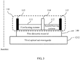
- There is a second dielectric material 141 between the third optical sub-waveguide 1212 and the fourth optical sub-waveguide 1222 A thermal conductivity of the first dielectric material 140 is greater than a thermal conductivity of the second dielectric material 141.
- the optical switch 100 includes the first optical waveguide 121, the second optical waveguide 122, and the first heater 110.
- the place at which the distance between the first optical waveguide 121 and the second optical waveguide 122 is the smallest is the junction.
- the first optical waveguide 121 includes the first optical sub-waveguide 1211 and the third optical sub-waveguide 1212.
- the second optical waveguide 122 includes the second optical sub-waveguide 1221 and the fourth optical sub-waveguide 1222.
- the first heater 110 is adjacent to the third optical sub-waveguide 1212.
- the thermal conductivity of the first dielectric material 140 is greater than the thermal conductivity of the second dielectric material.
- a material with a high thermal conductivity is used as the first dielectric material 140, to reduce heat dissipation and improve heating efficiency.
- a material with a low thermal conductivity is used as the second dielectric material 141, to further reduce dissipation of heat in the third optical sub-waveguide 1212, increase a difference between effective refractive indexes of the third optical sub-waveguide 1212 and the fourth optical sub-waveguide 1222, and further reduce a component length. Simulation shows that in this embodiment of the present invention, the difference between the effective refractive indexes of the third optical sub-waveguide 1212 and the fourth optical sub-waveguide 1222 may reach 0.01, and the component length may be shortened to 1 mm. This helps integration of a silicon-based large-scale digital optical switch array.
- the material with a high thermal conductivity such as aluminum oxide (Aluminum oxide, Al2O3) or silicon (Silicon, Si) may be used as the first dielectric material 140.
- Thermal conductivities of Al2O3 and Si are 130 and 35, respectively, in a unit of watts/meter* degree (W/m*K), representing heat that is transferred through an area of one square meter within one second when a material is 1 meter thick and a temperature difference between surfaces of two sides of the material is one degree.
- the material with a low thermal conductivity such as silicon dioxide (Silicon dioxide, Si02) or air may be used as the second dielectric material 141.
- the first heater 110 may be a metal heater, or a silicon doped heater, or the like. This is not limited in this embodiment of the present invention.
- the distance between the first optical waveguide 121 and the second optical waveguide 122 first decreases and then increases. That is, a distance between the first optical waveguide 121 and the second optical waveguide 122 at a place that is at a distance from the junction is greater than a distance between the first optical waveguide 121 and the second optical waveguide 122 at a place that is near the junction.
- An optical coupling relationship is formed at the junction, where the first optical waveguide 121 and the second optical waveguide 122 are not in contact. This reduces a requirement for a manufacturing process.
- a minimum distance between the first optical waveguide 121 and the second optical waveguide 122 may be 100 nm. A low-cost CMOS process can be used, and the requirement for the manufacturing process is reduced.
- a temperature difference between the third optical sub-waveguide 1212 and the fourth optical sub-waveguide 1222 gradually increases from the junction. That is, a temperature of the third optical sub-waveguide 1212 at a place that is at a distance from the junction is higher than a temperature of the third optical sub-waveguide 1212 at a place that is near the junction, and a temperature difference between the third optical sub-waveguide 1212 and the fourth optical sub-waveguide 1222 at a place that is at a distance from the junction is greater than a temperature difference between the third optical sub-waveguide 1212 and the fourth optical sub-waveguide 1222 at a place that is near the junction.
- evolution of an adiabatic mode is implemented, optical coupling efficiency may be improved, and loss and crosstalk may be reduced.
- the first heater 110 includes a first heating resistor 111, a second heating resistor 112, a first electrode 113, a second electrode 114, and a third electrode 115.
- the first heating resistor 111 is connected to the first dielectric material 140, and the first heating resistor 111 is located between the first electrode 113 and the second electrode 114.
- the second heating resistor 112 is connected to the first dielectric material 140, and the second heating resistor 112 is located between the second electrode 114 and the third electrode 115.
- a distance between the first electrode 113 and the junction, a distance between the second electrode 114 and the junction, and a distance between the third electrode 115 and the junction are in ascending order.
- the distance between the third electrode 115 and the junction is greater than the distance between the second electrode 114 and the junction, and the distance between the second electrode 114 and the junction is greater than the distance between the first electrode 113 and the junction.
- the first electrode 113 and the third electrode 115 have a same polarity, and the first electrode 113 and the second electrode 114 have opposite polarities.
- a distance between the first electrode 113 and the second electrode 114 is greater than a distance between the second electrode 114 and the third electrode 115.
- the distance between the first electrode 113 and the second electrode 114 is greater than the distance between the second electrode 114 and the third electrode 115, and therefore resistance of the first heating resistor 111 is greater than resistance of the second heating resistor 112, and the second heating resistor 112 has a larger heating power, and transfers a larger amount of heat to the third optical sub-waveguide 1212. That is, from the junction, a temperature of the third optical sub-waveguide 1212 gradually increases, and a temperature difference between the third optical sub-waveguide 1212 and the fourth optical sub-waveguide 1222 also gradually increases. In this way, evolution of an adiabatic mode is implemented, optical coupling efficiency may be improved, and loss and crosstalk may be reduced.
- the first heater 110 includes a first heating resistor 111, a second heating resistor 112, a first electrode 113, a second electrode 114, and a third electrode 115.
- the first heating resistor 111 is connected to the first dielectric material 140, and the first heating resistor 111 is located between the first electrode 113 and the second electrode 114.
- the second heating resistor 112 is connected to the first dielectric material 140, and the second heating resistor 112 is located between the second electrode 114 and the third electrode 115.
- a distance between the first electrode 113 and the junction, a distance between the second electrode 114 and the junction, and a distance between the third electrode 115 and the junction are in ascending order.
- the distance between the third electrode 115 and the junction is greater than the distance between the second electrode 114 and the junction, and the distance between the second electrode 114 and the junction is greater than the distance between the first electrode 113 and the junction.
- the first electrode 113 and the third electrode 115 have a same polarity, and the first electrode 113 and the second electrode 114 have opposite polarities.
- the first heating resistor 111 and the second heating resistor 112 have smaller areas of cross sections that are perpendicular to a transmission direction of a current. That is, for both the first heating resistor 111 and the second heating resistor 112, a cross section at a place that is at a distance from the junction are larger than a cross section at a place that is near the junction.
- the cross sections are perpendicular to the transmission direction of the current.
- the first heating resistor 111 and the second heating resistor 112 When being closer to the junction, the first heating resistor 111 and the second heating resistor 112 have smaller areas of cross sections that are perpendicular to the transmission direction of the current, and an area of a cross section of a heating resistor perpendicular to the transmission direction of the current is inversely proportional to resistance. Therefore, resistance of the first heating resistor 111 is greater than resistance of the second heating resistor 112, the second heating resistor 112 has a larger heating power, and transfers a larger amount of heat to the third optical sub-waveguide 1212. That is, from the junction, a temperature of the third optical sub-waveguide 1212 gradually increases, and a temperature difference between the third optical sub-waveguide 1212 and the fourth optical sub-waveguide 1222 also gradually increases. In this way, evolution of an adiabatic mode is implemented, optical coupling efficiency may be improved, and loss and crosstalk may be reduced.
- the heater shown in FIG. 4 is an implementation of the first heater 110, and when being farther away from the junction, the first heating resistor 111 and the second heating resistor 112 that are of a same length are thicker. That is, a cross section perpendicular to the transmission direction of the current at a place that is at a distance from the junction is larger than a cross section perpendicular to the transmission direction of the current at a place that is near the junction.
- the first heater 110 may further be in another form. This is not limited in this embodiment of the present invention.
- first heating resistor 111 and the second heating resistor 112 may be partially connected, or may be completely separated by the second electrode 114.
- the digital optical switch 100 further includes a second heater 150.
- the second heater 150 is adjacent to the third optical sub-waveguide 1212.
- a distance between the second heater 150 and the junction is greater than a distance between the first heater 110 and the junction.
- a heating power of the second heater 150 is greater than a heating power of the first heater 110.
- the second heater 150 has a heating power greater than the first heater 110 and is farther away from the junction than the first heater 110, and therefore a temperature difference between the third optical sub-waveguide 1212 and the fourth optical sub-waveguide 1222 may also begin to gradually increase from the junction. In this way, evolution of an adiabatic mode is implemented, optical coupling efficiency is improved, and loss and crosstalk are reduced.
- structures of the heaters may be relatively simple, and there may be more than two heaters. This is not limited in this embodiment of the present invention.
- a distance is larger between the first heater 110 and the third optical sub-waveguide 1212. That is, a distance between the first heater 110 and the third optical sub-waveguide 1212 at a place that is at a distance from the junction is less than a distance between the first heater 110 and the third optical sub-waveguide 1212 at a place that is near the junction. From the junction, in a process in which heat is transferred to the third optical sub-waveguide 1212, the first dielectric material 140 that heat needs to pass through gradually reduces, and an amount of heat dissipated in the first dielectric material 140 also gradually reduces.
- a temperature of the third optical sub-waveguide 1212 gradually increases, and a temperature difference between the third optical sub-waveguide 1212 and the fourth optical sub-waveguide 1222 also gradually increases. In this way, evolution of an adiabatic mode is implemented, optical coupling efficiency may be improved, and loss and crosstalk may be reduced.
- being adjacent to the third optical sub-waveguide 1212 specifically includes being on an outer side of or above the third optical sub-waveguide 1212.
- the outer side of the third optical sub-waveguide 1212 is a side not adjacent to the fourth optical sub-waveguide 1222.
- the heater may be farther away from the fourth optical sub-waveguide 1222, and a temperature difference between the third optical sub-waveguide 1212 and the fourth optical sub-waveguide 1222 may be larger.
- an effective refractive index of the third optical sub-waveguide 1212 is greater than an effective refractive index of the fourth optical sub-waveguide 1222, and from the junction, an increasing quantity of light fields of fundamental mode light are distributed in the third optical sub-waveguide 1212, and an increasing quantity of light fields of first-order mode light are distributed in the fourth optical sub-waveguide 1222.
- an effective refractive index of the third optical sub-waveguide 1212 is less than an effective refractive index of the fourth optical sub-waveguide 1222, and from the junction, an increasing quantity of light fields of fundamental mode light are distributed in the fourth optical sub-waveguide 1222, and an increasing quantity of light fields of first-order mode light are distributed in the third optical sub-waveguide 1212.
- An effective refractive index of an optical waveguide is an important parameter of the optical waveguide, and may be adjusted by changing a width, a height, or a temperature of the optical waveguide. If input light has a same wavelength and a same mode, a higher temperature of the optical waveguide indicates a larger effective refractive index of the optical waveguide; if the width of the optical waveguide does not change, a larger height also indicates a larger effective refractive index of the optical waveguide; and if the height of the optical waveguide does not change, a larger width also indicates a larger effective refractive index of the optical waveguide.
- the first optical waveguide 121 and the second optical waveguide 122 have a same height, a width of the first optical sub-waveguide 1211 is greater than a width of the second optical sub-waveguide 1221, and a width difference between the first optical sub-waveguide 1211 and the second optical sub-waveguide 1221 gradually decreases until reaching a minimum at the junction. That is, a width difference between the first optical sub-waveguide 1211 and the second optical sub-waveguide 1221 at a place that is at a distance from the junction is greater than a width difference between the first optical sub-waveguide 1211 and the second optical sub-waveguide 1221 at a place that is near the junction.
- an effective refractive index of the first optical sub-waveguide 1211 is greater than an effective refractive index of the second optical sub-waveguide 1221, and a difference between the effective refractive indexes of the first optical sub-waveguide 1211 and the second optical sub-waveguide 1221 gradually decreases until reaching a minimum at the junction, so that when the first heater 110 is not operating, from the junction, an increasing quantity of light fields of fundamental mode light are distributed in the first optical sub-waveguide 1211, and an increasing quantity of light fields of first-order mode light are distributed in the second optical sub-waveguide 1221.
- a width of the third optical sub-waveguide 1212 is less than a width of the fourth optical sub-waveguide 1222. From the junction, a width difference between the third optical sub-waveguide 1212 and the fourth optical sub-waveguide 1222 gradually increases. That is, a width difference between the third optical sub-waveguide 1212 and the fourth optical sub-waveguide 1222 at a place that is at a distance from the junction is greater than a width difference between the third optical sub-waveguide 1212 and the fourth optical sub-waveguide 1222 at a place that is near the junction.
- an effective refractive index of the third optical sub-waveguide 1212 is less than an effective refractive index of the fourth optical sub-waveguide 1222, and a difference between the effective refractive indexes of the third optical sub-waveguide 1212 and the fourth optical sub-waveguide 1222 gradually decreases until reaching a minimum at the junction, so that when the first heater 110 is not operating, from the junction, an increasing quantity of light fields of the fundamental mode light are distributed in the fourth optical sub-waveguide 1222, and an increasing quantity of light fields of the first-order mode light are distributed in the third optical sub-waveguide 1212.
- a difference between effective refractive indexes may reach 0.01.
- the difference between the effective refractive indexes reaches 0.01, more than 99% of the fundamental mode light is distributed in an optical waveguide with a larger effective refractive index, and more than 99% of the first-order mode light is distributed in an optical waveguide with a smaller effective refractive index.
- an optical waveguide is made of a Si material.
- a basic principle is that light field distribution of signal light is changed by adjusting an effective refractive index of the optical waveguide, to switch an optical path.
- the first optical waveguide 121 and the second optical waveguide 122 have the same height, the width of the first optical sub-waveguide 1211 is greater than the width of the second optical sub-waveguide 1221, and therefore the effective refractive index of the first optical sub-waveguide 1211 is greater than the effective refractive index of the second optical sub-waveguide 1221.
- a symmetric mode is triggered, and the fundamental mode light is generated. As shown in FIG.
- the width difference between the first optical sub-waveguide 1211 and the second optical sub-waveguide 1221 is the smallest, and a fundamental mode light distribution difference between the first optical sub-waveguide 1211 and the second optical sub-waveguide 1221 is also the smallest.
- the width of the third optical sub-waveguide 1212 is less than the width of the fourth optical sub-waveguide 1222, the width difference gradually increases, and therefore the fundamental mode light continues to be transferred to the fourth optical sub-waveguide 1222, and when being output finally, the fundamental mode light is output from the fourth optical sub-waveguide 1222.
- the first-order mode light is generated.
- the width difference between the first optical sub-waveguide 1211 and the second optical sub-waveguide 1221 is the smallest, and a first-order mode light distribution difference between the first optical sub-waveguide 1211 and the second optical sub-waveguide 1221 is also the smallest.
- the width of the third optical sub-waveguide 1212 is less than the width of the fourth optical sub-waveguide 1222, the width difference gradually increases, and therefore the first-order mode light continues to be transferred to the third optical sub-waveguide 1212, and when being output finally, the first-order mode light is output from the third optical sub-waveguide 1212.
- the digital optical switch 100 is in a cross-connect state, and the first heater 110 does not need to operate, thereby reducing control complexity and power consumption.
- an optical signal input from the second optical sub-waveguide 1221 is equivalent to an optical signal output from the third optical sub-waveguide 1212.
- lights input from the first optical sub-waveguide 1211 and the second optical sub-waveguide 1221 do not affect each other.
- the first heater 110 starts to operate, a temperature of the third optical sub-waveguide 1212 rises.
- the effective refractive index of the optical waveguide that is made of the Si material increases with an increasing temperature, and therefore the effective refractive index of the third optical sub-waveguide 1212 is greater than the effective refractive index of the fourth optical sub-waveguide 1222.
- the light input from the first optical sub-waveguide 1211 is output from the third optical sub-waveguide 1212
- the light input from the second optical sub-waveguide 1221 is output from the fourth optical sub-waveguide 1222.
- the digital optical switch 100 operates in a straight-through state. In this case, for the digital optical switch 100, only the first heater 110 needs to operate. That is, in this embodiment of the present invention, only one heater is required in total, thereby reducing control complexity and power consumption.
- the first optical waveguide 121 and the second optical waveguide 122 have a same height, a width of the first optical sub-waveguide 1211 is less than a width of the second optical sub-waveguide 1221, and a width difference between the first optical sub-waveguide 1211 and the second optical sub-waveguide 1221 gradually decreases until reaching a minimum at the junction. That is, a width difference between the first optical sub-waveguide 1211 and the second optical sub-waveguide 1221 at a place that is at a distance from the junction is greater than a width difference between the first optical sub-waveguide 1211 and the second optical sub-waveguide 1221 at a place that is near the junction.
- an effective refractive index of the first optical sub-waveguide 1211 is less than an effective refractive index of the second optical sub-waveguide 1221, and a difference between the effective refractive indexes of the first optical sub-waveguide 1211 and the second optical sub-waveguide 1221 gradually decreases until reaching a minimum at the junction, so that when the first heater 110 is not operating, from the junction, an increasing quantity of light fields of fundamental mode light are distributed in the first optical sub-waveguide 1211, and an increasing quantity of light fields of first-order mode light are distributed in the second optical sub-waveguide 1221.
- a width of the third optical sub-waveguide 1212 is less than a width of the fourth optical sub-waveguide 1222. From the junction, a width difference between the third optical sub-waveguide 1212 and the fourth optical sub-waveguide 1222 gradually increases. That is, a width difference between the third optical sub-waveguide 1212 and the fourth optical sub-waveguide 1222 at a place that is at a distance from the junction is greater than a width difference between the third optical sub-waveguide 1212 and the fourth optical sub-waveguide 1222 at a place that is near the junction.
- an effective refractive index of the third optical sub-waveguide 1212 is less than an effective refractive index of the fourth optical sub-waveguide 1222, and a difference between the effective refractive indexes of the third optical sub-waveguide 1212 and the fourth optical sub-waveguide 1222 gradually decreases until reaching a minimum at the junction, so that when the first heater 110 is not operating, from the junction, an increasing quantity of light fields of the fundamental mode light are distributed in the third optical sub-waveguide 1212, and an increasing quantity of light fields of the first-order mode light are distributed in the fourth optical sub-waveguide 1222.
- the first optical waveguide 121 and the second optical waveguide 122 have a same height, a width of the first optical sub-waveguide 1211 is greater than a width of the second optical sub-waveguide 1221, and a width difference between the first optical sub-waveguide 1211 and the second optical sub-waveguide 1221 gradually decreases until reaching a minimum at the junction. That is, a width difference between the first optical sub-waveguide 1211 and the second optical sub-waveguide 1221 at a place that is at a distance from the junction is greater than a width difference between the first optical sub-waveguide 1211 and the second optical sub-waveguide 1221 at a place that is near the junction.
- an effective refractive index of the first optical sub-waveguide 1211 is greater than an effective refractive index of the second optical sub-waveguide 1221, and a difference between the effective refractive indexes of the first optical sub-waveguide 1211 and the second optical sub-waveguide 1221 gradually decreases until reaching a minimum at the junction, so that when the first heater 110 is not operating, from the junction, an increasing quantity of light fields of fundamental mode light are distributed in the first optical sub-waveguide 1211, and an increasing quantity of light fields of first-order mode light are distributed in the second optical sub-waveguide 1221.
- Widths of the third optical sub-waveguide 1212 and the fourth optical sub-waveguide 1222 remain unchanged.
- effective refractive indexes of the third optical sub-waveguide 1212 and the fourth optical sub-waveguide 1222 are basically the same.
- an optical waveguide is made of a Si material.
- the first optical waveguide 121 and the second optical waveguide 122 have the same height, the width of the first optical sub-waveguide 1211 is greater than the width of the second optical sub-waveguide 1221, and therefore the effective refractive index of the first optical sub-waveguide 1211 is greater than the effective refractive index of the second optical sub-waveguide 1221.
- first optical sub-waveguide 1211 and the second optical sub-waveguide 1221 gradually approach the junction, a distance between the first optical sub-waveguide 1211 and the second optical sub-waveguide 1221 gradually decreases, optical coupling gradually increases, the width difference between the first optical sub-waveguide 1211 and the second optical sub-waveguide 1221 gradually decreases until reaching a minimum at the junction, and the light fields of the fundamental mode light are gradually transferred from the first optical sub-waveguide 1211 to the second optical sub-waveguide 1221, where the light fields of the fundamental mode light are originally distributed only in the first optical sub-waveguide 1211.
- the width difference between the first optical sub-waveguide 1211 and the second optical sub-waveguide 1221 is the smallest, and a fundamental mode light distribution difference between the first optical sub-waveguide 1211 and the second optical sub-waveguide 1221 is also the smallest.
- the first heater 110 is started, the effective refractive index of the third optical sub-waveguide 1212 is greater than the effective refractive index of the fourth optical sub-waveguide 1222, the fundamental mode light continues to be transferred to the third optical sub-waveguide 1212, and when being output finally, the fundamental mode light is output from the third optical sub-waveguide 1212.
- the first-order mode light is generated.
- a distance between the first optical sub-waveguide 1211 and the second optical sub-waveguide 1221 gradually decreases, optical coupling gradually increases, the width difference between the first optical sub-waveguide 1211 and the second optical sub-waveguide 1221 gradually decreases until reaching a minimum at the junction, the light fields of the first-order mode light are gradually transferred from the second optical sub-waveguide 1221 to the first optical sub-waveguide 1211, and a reverse light field component is formed in the first optical sub-waveguide 1211, where the light fields of the first-order mode light are originally distributed only in the second optical sub-waveguide 1221.
- the width difference between the first optical sub-waveguide 1211 and the second optical sub-waveguide 1221 is the smallest, and a first-order mode light distribution difference between the first-order mode light in the first optical sub-waveguide 1211 and the second optical sub-waveguide 1221 is also the smallest.
- the first heater 110 is started, the effective refractive index of the third optical sub-waveguide 1212 is greater than the effective refractive index of the fourth optical sub-waveguide 1222, the first-order mode light continues to be transferred to the fourth optical sub-waveguide 1222, and when being output finally, the first-order mode light is output from the fourth optical sub-waveguide 1222.
- the digital optical switch 100 is in a straight-through state, and only the first heater 110 needs to operate, thereby reducing control complexity and power consumption.
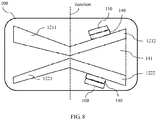
- the digital optical switch 100 further includes a third heater 160.
- the third heater 160 is adjacent to the fourth optical sub-waveguide 1222.
- the third heater 160 provides heat for the fourth optical sub-waveguide 1222.
- An effective refractive index of a Si material increases with a temperature, and therefore an effective refractive index of the fourth optical sub-waveguide 1222 is greater than an effective refractive index of the third optical sub-waveguide 1212.
- light input from the first optical sub-waveguide 1211 is output from the fourth optical sub-waveguide 1222
- light input from the second optical sub-waveguide 1221 is output from the third optical sub-waveguide 1212.
- the digital optical switch 100 operates in a cross-connect state. In this case, only the third heater 160 needs to operate in this embodiment of the present invention.
- this embodiment of the present invention has a relatively low requirement for temperatures of the first heater 110 and the third heater 160, and is easier to implement.
- an effective refractive index of the third optical sub-waveguide 1212 is greater than an effective refractive index of the fourth optical sub-waveguide 1222, and from the junction, an increasing quantity of light fields of fundamental mode light are distributed in the third optical sub-waveguide 1212, and an increasing quantity of light fields of first-order mode light are distributed in the fourth optical sub-waveguide 1222.
- an effective refractive index of the third optical sub-waveguide 1212 is less than an effective refractive index of the fourth optical sub-waveguide 1222, and from the junction, an increasing quantity of light fields of fundamental mode light are distributed in the fourth optical sub-waveguide 1222, and an increasing quantity of light fields of first-order mode light are distributed in the third optical sub-waveguide 1212.
- being adjacent to the fourth optical sub-waveguide 1222 specifically includes being on an outer side of or above the fourth optical sub-waveguide 1222.
- the outer side of the fourth optical sub-waveguide 1222 is a side not adjacent to the third optical sub-waveguide 1212.
- the third heater 160 may be farther away from the third optical sub-waveguide 1212, and a temperature difference between the third optical sub-waveguide 1212 and the fourth optical sub-waveguide 1222 may be larger.
- the first dielectric material 140 between the third heater 160 and the fourth optical sub-waveguide 1222.
- a material with a high thermal conductivity is used as the first dielectric material 140 to improve heating efficiency.
- the first optical waveguide 121 and the second optical waveguide 122 have a same width, a height of the first optical sub-waveguide 1211 is greater than a height of the second optical sub-waveguide 1221, and a height difference between the first optical sub-waveguide 1211 and the second optical sub-waveguide 1221 gradually decreases until reaching a minimum at the junction.
- a height difference between the first optical sub-waveguide 1211 and the second optical sub-waveguide 1221 at a place that is at a distance from the junction is greater than a height difference between the first optical sub-waveguide 1211 and the second optical sub-waveguide 1221 at a place that is near the junction, so that when the first heater 110 is not operating, from the junction, an increasing quantity of light fields of fundamental mode light are distributed in the first optical sub-waveguide 1211, and an increasing quantity of light fields of first-order mode light are distributed in the second optical sub-waveguide 1221.
- an effective refractive index of the first optical sub-waveguide 1211 is greater than an effective refractive index of the second optical sub-waveguide 1221, and a difference between the effective refractive indexes of the first optical sub-waveguide 1211 and the second optical sub-waveguide 1221 gradually decreases until reaching a minimum at the junction.
- a height of the third optical sub-waveguide 1212 is less than a height of the fourth optical sub-waveguide 1222. From the junction, a height difference between the third optical sub-waveguide 1212 and the fourth optical sub-waveguide 1222 gradually increases. That is, a height difference between the third optical sub-waveguide 1212 and the fourth optical sub-waveguide 1222 at a place that is at a distance from the junction is greater than a height difference between the third optical sub-waveguide 1212 and the fourth optical sub-waveguide 1222 at a place that is near the junction.
- an effective refractive index of the third optical sub-waveguide 1212 is less than an effective refractive index of the fourth optical sub-waveguide 1222, and a difference between the effective refractive indexes of the third optical sub-waveguide 1212 and the fourth optical sub-waveguide 1222 gradually decreases until reaching a minimum at the junction, so that when the first heater 110 is not operating, from the junction, an increasing quantity of light fields of the fundamental mode light are distributed in the fourth optical sub-waveguide 1222, and an increasing quantity of light fields of the first-order mode light are distributed in the third optical sub-waveguide 1212.
- the effective refractive index of the first optical sub-waveguide 1211 is greater than the effective refractive index of the second optical sub-waveguide 1221.
- the first optical waveguide 121 and the second optical waveguide 122 have a same width, a height of the first optical sub-waveguide 1211 is less than a height of the second optical sub-waveguide 1221, and a height difference between the first optical sub-waveguide 1211 and the second optical sub-waveguide 1221 gradually decreases until reaching a minimum at the junction.
- a height difference between the first optical sub-waveguide 1211 and the second optical sub-waveguide 1221 at a place that is at a distance from the junction is greater than a height difference between the first optical sub-waveguide 1211 and the second optical sub-waveguide 1221 at a place that is near the junction, so that when the first heater 110 is not operating, from the junction, an increasing quantity of light fields of fundamental mode light are distributed in the first optical sub-waveguide 1211, and an increasing quantity of light fields of first-order mode light are distributed in the second optical sub-waveguide 1221.
- a height of the third optical sub-waveguide 1212 is less than a height of the fourth optical sub-waveguide 1222. From the junction, a height difference between the third optical sub-waveguide 1212 and the fourth optical sub-waveguide 1222 gradually increases. That is, a height difference between the third optical sub-waveguide 1212 and the fourth optical sub-waveguide 1222 at a place that is at a distance from the junction is greater than a height difference between the third optical sub-waveguide 1212 and the fourth optical sub-waveguide 1222 at a place that is near the junction, so that when the first heater 110 is not operating, from the junction, an increasing quantity of light fields of the fundamental mode light are distributed in the third optical sub-waveguide 1212, and an increasing quantity of light fields of the first-order mode light are distributed in the fourth optical sub-waveguide 1222.
- the first optical waveguide 121 and the second optical waveguide 122 have a same width, a height of the first optical sub-waveguide 1211 is greater than a height of the second optical sub-waveguide 1221, and a height difference between the first optical sub-waveguide 1211 and the second optical sub-waveguide 1221 gradually decreases until reaching a minimum at the junction.
- a height difference between the first optical sub-waveguide 1211 and the second optical sub-waveguide 1221 at a place that is at a distance from the junction is greater than a height difference between the first optical sub-waveguide 1211 and the second optical sub-waveguide 1221 at a place that is near the junction, so that when the first heater 110 is not operating, from the junction, an increasing quantity of light fields of fundamental mode light are distributed in the first optical sub-waveguide 1211, and an increasing quantity of light fields of first-order mode light are distributed in the second optical sub-waveguide 1221. Heights of the third optical sub-waveguide 1212 and the fourth optical sub-waveguide 1222 remain unchanged. If neither the first heater 110 nor the third heater 160 is operating, effective refractive indexes of the third optical sub-waveguide 1212 and the fourth optical sub-waveguide 1222 are basically equal.
- this embodiment of the present invention two heaters are required in total, but only one heater needs to be in an operating state at a time, thereby reducing control complexity and power consumption.
- this embodiment of the present invention has a relatively low requirement for temperatures of the first heater 110 and the third heater 160, and is easier to implement. A specific working process has been described in detail in the previous embodiments, and details are not described in this embodiment of the present invention.
Landscapes
- Physics & Mathematics (AREA)
- Nonlinear Science (AREA)
- General Physics & Mathematics (AREA)
- Optics & Photonics (AREA)
- Engineering & Computer Science (AREA)
- Microelectronics & Electronic Packaging (AREA)
- Optical Modulation, Optical Deflection, Nonlinear Optics, Optical Demodulation, Optical Logic Elements (AREA)
Applications Claiming Priority (3)
| Application Number | Priority Date | Filing Date | Title |
|---|---|---|---|
| CN201610288760 | 2016-05-04 | ||
| CN201610619006.6A CN107346047B (zh) | 2016-05-04 | 2016-07-29 | 一种光开关 |
| PCT/CN2016/104051 WO2017190481A1 (fr) | 2016-05-04 | 2016-10-31 | Commutateur optique |
Publications (3)
| Publication Number | Publication Date |
|---|---|
| EP3441817A1 true EP3441817A1 (fr) | 2019-02-13 |
| EP3441817A4 EP3441817A4 (fr) | 2019-07-10 |
| EP3441817B1 EP3441817B1 (fr) | 2023-12-20 |
Family
ID=60254320
Family Applications (1)
| Application Number | Title | Priority Date | Filing Date |
|---|---|---|---|
| EP16901003.0A Active EP3441817B1 (fr) | 2016-05-04 | 2016-10-31 | Commutateur optique |
Country Status (3)
| Country | Link |
|---|---|
| US (1) | US10481466B2 (fr) |
| EP (1) | EP3441817B1 (fr) |
| CN (1) | CN107346047B (fr) |
Families Citing this family (4)
| Publication number | Priority date | Publication date | Assignee | Title |
|---|---|---|---|---|
| CN107346047B (zh) * | 2016-05-04 | 2020-04-21 | 华为技术有限公司 | 一种光开关 |
| CN111856650B (zh) * | 2019-04-30 | 2021-10-19 | 华为技术有限公司 | 常暗光开关和光路选通装置 |
| US11609374B2 (en) * | 2021-03-22 | 2023-03-21 | Taiwan Semiconductor Manufacturing Company, Ltd. | Directionally tunable optical reflector |
| CN120928624B (zh) * | 2025-10-13 | 2026-03-06 | 上海图灵智算量子科技有限公司 | 波导组件、波导组件的控制方法、光芯片及光量子计算机 |
Family Cites Families (23)
| Publication number | Priority date | Publication date | Assignee | Title |
|---|---|---|---|---|
| US4846540A (en) * | 1988-01-25 | 1989-07-11 | Bell Communications Research, Inc. | Optical wavegide junction |
| US5033811A (en) * | 1988-11-04 | 1991-07-23 | The Furukawa Electric Co., Ltd. | Optical switch |
| NL9001157A (nl) | 1990-05-17 | 1991-12-16 | Nederland Ptt | Digitale optische schakelaar. |
| FR2728083B1 (fr) | 1994-12-08 | 1997-01-10 | Alcatel Nv | Commutateur optique binaire compact |
| US6094516A (en) * | 1995-04-03 | 2000-07-25 | Nolting; Hans-Peter | Digital optical switch |
| EP0821809A1 (fr) * | 1995-04-18 | 1998-02-04 | Akzo Nobel N.V. | Dispositif thermo-optique asymetrique a commutation rapide |
| DE19623888A1 (de) * | 1996-06-05 | 1997-12-11 | Hertz Inst Heinrich | Digitaler optischer Schalter |
| KR100326046B1 (ko) | 1999-06-21 | 2002-03-07 | 윤종용 | 열광학 스위치 및 그 제작방법 |
| DE60127146T2 (de) * | 2000-09-18 | 2007-11-22 | Ngk Insulators, Ltd., Nagoya | Optische vorrichtung |
| AUPR174300A0 (en) * | 2000-11-28 | 2000-12-21 | Redfern Integrated Optics Pty Ltd | Thermo optical phase shifter with reduced power consumption |
| JP3929844B2 (ja) | 2002-02-19 | 2007-06-13 | 株式会社フジクラ | 光スイッチ、光アドドロップモジュール及び光通信システム |
| CN100408358C (zh) * | 2003-01-23 | 2008-08-06 | 米其林技术公司 | 包括刚性元件的轮胎 |
| US7590312B2 (en) * | 2003-07-04 | 2009-09-15 | Nippon Telegraph And Telephone Corporation | Interferometer optical switch and variable optical attenuator |
| JP2005064051A (ja) * | 2003-08-14 | 2005-03-10 | Fibest Ltd | 光モジュールおよび光通信システム |
| CN1320400C (zh) | 2003-11-01 | 2007-06-06 | 浙江大学 | 低串扰数字光开关 |
| CN1651950A (zh) * | 2004-01-26 | 2005-08-10 | 林克斯光化网络公司 | 平面光波电路中的高容限宽带光开关 |
| JP4997481B2 (ja) * | 2004-09-01 | 2012-08-08 | パナソニック株式会社 | 光スイッチ |
| JP2006208518A (ja) * | 2005-01-26 | 2006-08-10 | Seikoh Giken Co Ltd | 熱光学効果型光導波路素子およびその製造方法 |
| JP2007114253A (ja) * | 2005-10-18 | 2007-05-10 | Hitachi Cable Ltd | 導波路型光分岐素子 |
| KR101165715B1 (ko) * | 2008-12-10 | 2012-07-18 | 한국전자통신연구원 | 광 스위치를 포함하는 광통신 소자 |
| JP4745415B2 (ja) * | 2009-03-31 | 2011-08-10 | 住友大阪セメント株式会社 | 光変調器 |
| CN102944913A (zh) | 2012-11-22 | 2013-02-27 | 中国科学院半导体研究所 | 一种基于耦合模式分离的光分束器 |
| CN107346047B (zh) * | 2016-05-04 | 2020-04-21 | 华为技术有限公司 | 一种光开关 |
-
2016
- 2016-07-29 CN CN201610619006.6A patent/CN107346047B/zh active Active
- 2016-10-31 EP EP16901003.0A patent/EP3441817B1/fr active Active
-
2018
- 2018-11-02 US US16/179,631 patent/US10481466B2/en active Active
Also Published As
| Publication number | Publication date |
|---|---|
| EP3441817A4 (fr) | 2019-07-10 |
| CN107346047B (zh) | 2020-04-21 |
| EP3441817B1 (fr) | 2023-12-20 |
| US10481466B2 (en) | 2019-11-19 |
| CN107346047A (zh) | 2017-11-14 |
| US20190086764A1 (en) | 2019-03-21 |
Similar Documents
| Publication | Publication Date | Title |
|---|---|---|
| Suzuki et al. | Low-insertion-loss and power-efficient 32× 32 silicon photonics switch with extremely high-Δ silica PLC connector | |
| Kita et al. | Ultrafast silicon MZI optical switch with periodic electrodes and integrated heat sink | |
| US10481466B2 (en) | Optical switch | |
| KR101063957B1 (ko) | 폴리머 삽입형 실리카 광도파로를 이용하는 전반사형 광 스위치 및 그의 제조 방법 | |
| JP2010517113A (ja) | 熱光学導波路装置 | |
| CN113900280A (zh) | 偏振无关的光开关 | |
| CN113625392B (zh) | 一种基于有机无机混合集成的4×4光开关阵列 | |
| CN109709644B (zh) | 一种基于soi材料制备的跑道型微环2×4热光开关 | |
| CN103293713B (zh) | 一种高效紧凑的马赫-曾德尔光开关结构 | |
| CN113985522B (zh) | 基于硅-氮化硅三维集成的微环光开关 | |
| CN217181269U (zh) | 一种基于相变材料的2×2光波导开关 | |
| CN106371175A (zh) | 一种高效紧凑无阻塞型4×4波导光开关矩阵 | |
| US7389033B2 (en) | Planar lightwave circuit type variable optical attenuator | |
| Liang et al. | N× N reconfigurable nonblocking polymer/silica hybrid planar optical switch matrix based on total-internal-reflection effect | |
| CN116736564A (zh) | 一种基于石墨烯电极的聚合物三维波导模式光开关 | |
| CN116027482A (zh) | 多模光路由状态切换单元及多模光开关 | |
| Han et al. | 2$\,\times\, $2 Polymer Thermo-Optic Digital Optical Switch Using Total-Internal-Reflection in Bend-Free Waveguides | |
| CN107111169A (zh) | 应力调谐平面照明电路及其方法 | |
| Sun et al. | New concept of silicon photonic MEMS switch based on total internal reflection | |
| Li et al. | 4× 4 strictly non-blocking optical switch fabric based on cascaded multimode interferometers | |
| Iino et al. | Compact Silicon MZI Optical Switch with Low Thermal-crosstalk | |
| CN105182568A (zh) | 一种低损耗超宽带的热光开关 | |
| JPH01201628A (ja) | 光スイッチ | |
| CN113759469B (zh) | 一种偏振不敏感的双通道双波长选择开关 | |
| WO2017190481A1 (fr) | Commutateur optique |
Legal Events
| Date | Code | Title | Description |
|---|---|---|---|
| STAA | Information on the status of an ep patent application or granted ep patent |
Free format text: STATUS: THE INTERNATIONAL PUBLICATION HAS BEEN MADE |
|
| PUAI | Public reference made under article 153(3) epc to a published international application that has entered the european phase |
Free format text: ORIGINAL CODE: 0009012 |
|
| STAA | Information on the status of an ep patent application or granted ep patent |
Free format text: STATUS: REQUEST FOR EXAMINATION WAS MADE |
|
| 17P | Request for examination filed |
Effective date: 20181107 |
|
| AK | Designated contracting states |
Kind code of ref document: A1 Designated state(s): AL AT BE BG CH CY CZ DE DK EE ES FI FR GB GR HR HU IE IS IT LI LT LU LV MC MK MT NL NO PL PT RO RS SE SI SK SM TR |
|
| AX | Request for extension of the european patent |
Extension state: BA ME |
|
| RIC1 | Information provided on ipc code assigned before grant |
Ipc: G02F 1/313 20060101AFI20190301BHEP Ipc: G02B 6/125 20060101ALI20190301BHEP |
|
| A4 | Supplementary search report drawn up and despatched |
Effective date: 20190611 |
|
| RIC1 | Information provided on ipc code assigned before grant |
Ipc: G02B 6/125 20060101ALI20190604BHEP Ipc: G02F 1/313 20060101AFI20190604BHEP |
|
| DAV | Request for validation of the european patent (deleted) | ||
| DAX | Request for extension of the european patent (deleted) | ||
| STAA | Information on the status of an ep patent application or granted ep patent |
Free format text: STATUS: EXAMINATION IS IN PROGRESS |
|
| 17Q | First examination report despatched |
Effective date: 20210521 |
|
| REG | Reference to a national code |
Ref country code: DE Free format text: PREVIOUS MAIN CLASS: G02F0001313000 Ref country code: DE Ref legal event code: R079 Ref document number: 602016084911 Country of ref document: DE Free format text: PREVIOUS MAIN CLASS: G02F0001313000 Ipc: G02F0001010000 |
|
| RIC1 | Information provided on ipc code assigned before grant |
Ipc: G02F 1/313 20060101ALI20230703BHEP Ipc: G02F 1/01 20060101AFI20230703BHEP |
|
| GRAP | Despatch of communication of intention to grant a patent |
Free format text: ORIGINAL CODE: EPIDOSNIGR1 |
|
| STAA | Information on the status of an ep patent application or granted ep patent |
Free format text: STATUS: GRANT OF PATENT IS INTENDED |
|
| INTG | Intention to grant announced |
Effective date: 20230814 |
|
| RIN1 | Information on inventor provided before grant (corrected) |
Inventor name: TU, XIN Inventor name: LI, MING Inventor name: XING, JIEJIANG |
|
| GRAS | Grant fee paid |
Free format text: ORIGINAL CODE: EPIDOSNIGR3 |
|
| GRAA | (expected) grant |
Free format text: ORIGINAL CODE: 0009210 |
|
| STAA | Information on the status of an ep patent application or granted ep patent |
Free format text: STATUS: THE PATENT HAS BEEN GRANTED |
|
| AK | Designated contracting states |
Kind code of ref document: B1 Designated state(s): AL AT BE BG CH CY CZ DE DK EE ES FI FR GB GR HR HU IE IS IT LI LT LU LV MC MK MT NL NO PL PT RO RS SE SI SK SM TR |
|
| REG | Reference to a national code |
Ref country code: GB Ref legal event code: FG4D |
|
| P01 | Opt-out of the competence of the unified patent court (upc) registered |
Effective date: 20231121 |
|
| REG | Reference to a national code |
Ref country code: CH Ref legal event code: EP |
|
| REG | Reference to a national code |
Ref country code: DE Ref legal event code: R096 Ref document number: 602016084911 Country of ref document: DE |
|
| REG | Reference to a national code |
Ref country code: IE Ref legal event code: FG4D |
|
| PG25 | Lapsed in a contracting state [announced via postgrant information from national office to epo] |
Ref country code: GR Free format text: LAPSE BECAUSE OF FAILURE TO SUBMIT A TRANSLATION OF THE DESCRIPTION OR TO PAY THE FEE WITHIN THE PRESCRIBED TIME-LIMIT Effective date: 20240321 |
|
| REG | Reference to a national code |
Ref country code: LT Ref legal event code: MG9D |
|
| PG25 | Lapsed in a contracting state [announced via postgrant information from national office to epo] |
Ref country code: LT Free format text: LAPSE BECAUSE OF FAILURE TO SUBMIT A TRANSLATION OF THE DESCRIPTION OR TO PAY THE FEE WITHIN THE PRESCRIBED TIME-LIMIT Effective date: 20231220 |
|
| REG | Reference to a national code |
Ref country code: NL Ref legal event code: MP Effective date: 20231220 |
|
| PG25 | Lapsed in a contracting state [announced via postgrant information from national office to epo] |
Ref country code: ES Free format text: LAPSE BECAUSE OF FAILURE TO SUBMIT A TRANSLATION OF THE DESCRIPTION OR TO PAY THE FEE WITHIN THE PRESCRIBED TIME-LIMIT Effective date: 20231220 |
|
| PG25 | Lapsed in a contracting state [announced via postgrant information from national office to epo] |
Ref country code: LT Free format text: LAPSE BECAUSE OF FAILURE TO SUBMIT A TRANSLATION OF THE DESCRIPTION OR TO PAY THE FEE WITHIN THE PRESCRIBED TIME-LIMIT Effective date: 20231220 Ref country code: GR Free format text: LAPSE BECAUSE OF FAILURE TO SUBMIT A TRANSLATION OF THE DESCRIPTION OR TO PAY THE FEE WITHIN THE PRESCRIBED TIME-LIMIT Effective date: 20240321 Ref country code: FI Free format text: LAPSE BECAUSE OF FAILURE TO SUBMIT A TRANSLATION OF THE DESCRIPTION OR TO PAY THE FEE WITHIN THE PRESCRIBED TIME-LIMIT Effective date: 20231220 Ref country code: ES Free format text: LAPSE BECAUSE OF FAILURE TO SUBMIT A TRANSLATION OF THE DESCRIPTION OR TO PAY THE FEE WITHIN THE PRESCRIBED TIME-LIMIT Effective date: 20231220 Ref country code: BG Free format text: LAPSE BECAUSE OF FAILURE TO SUBMIT A TRANSLATION OF THE DESCRIPTION OR TO PAY THE FEE WITHIN THE PRESCRIBED TIME-LIMIT Effective date: 20240320 |
|
| REG | Reference to a national code |
Ref country code: AT Ref legal event code: MK05 Ref document number: 1642966 Country of ref document: AT Kind code of ref document: T Effective date: 20231220 |
|
| PG25 | Lapsed in a contracting state [announced via postgrant information from national office to epo] |
Ref country code: NL Free format text: LAPSE BECAUSE OF FAILURE TO SUBMIT A TRANSLATION OF THE DESCRIPTION OR TO PAY THE FEE WITHIN THE PRESCRIBED TIME-LIMIT Effective date: 20231220 |
|
| PG25 | Lapsed in a contracting state [announced via postgrant information from national office to epo] |
Ref country code: SE Free format text: LAPSE BECAUSE OF FAILURE TO SUBMIT A TRANSLATION OF THE DESCRIPTION OR TO PAY THE FEE WITHIN THE PRESCRIBED TIME-LIMIT Effective date: 20231220 Ref country code: RS Free format text: LAPSE BECAUSE OF FAILURE TO SUBMIT A TRANSLATION OF THE DESCRIPTION OR TO PAY THE FEE WITHIN THE PRESCRIBED TIME-LIMIT Effective date: 20231220 Ref country code: NO Free format text: LAPSE BECAUSE OF FAILURE TO SUBMIT A TRANSLATION OF THE DESCRIPTION OR TO PAY THE FEE WITHIN THE PRESCRIBED TIME-LIMIT Effective date: 20240320 Ref country code: NL Free format text: LAPSE BECAUSE OF FAILURE TO SUBMIT A TRANSLATION OF THE DESCRIPTION OR TO PAY THE FEE WITHIN THE PRESCRIBED TIME-LIMIT Effective date: 20231220 Ref country code: LV Free format text: LAPSE BECAUSE OF FAILURE TO SUBMIT A TRANSLATION OF THE DESCRIPTION OR TO PAY THE FEE WITHIN THE PRESCRIBED TIME-LIMIT Effective date: 20231220 Ref country code: HR Free format text: LAPSE BECAUSE OF FAILURE TO SUBMIT A TRANSLATION OF THE DESCRIPTION OR TO PAY THE FEE WITHIN THE PRESCRIBED TIME-LIMIT Effective date: 20231220 |
|
| PG25 | Lapsed in a contracting state [announced via postgrant information from national office to epo] |
Ref country code: IS Free format text: LAPSE BECAUSE OF FAILURE TO SUBMIT A TRANSLATION OF THE DESCRIPTION OR TO PAY THE FEE WITHIN THE PRESCRIBED TIME-LIMIT Effective date: 20240420 |
|
| PG25 | Lapsed in a contracting state [announced via postgrant information from national office to epo] |
Ref country code: CZ Free format text: LAPSE BECAUSE OF FAILURE TO SUBMIT A TRANSLATION OF THE DESCRIPTION OR TO PAY THE FEE WITHIN THE PRESCRIBED TIME-LIMIT Effective date: 20231220 Ref country code: AT Free format text: LAPSE BECAUSE OF FAILURE TO SUBMIT A TRANSLATION OF THE DESCRIPTION OR TO PAY THE FEE WITHIN THE PRESCRIBED TIME-LIMIT Effective date: 20231220 |
|
| PG25 | Lapsed in a contracting state [announced via postgrant information from national office to epo] |
Ref country code: SK Free format text: LAPSE BECAUSE OF FAILURE TO SUBMIT A TRANSLATION OF THE DESCRIPTION OR TO PAY THE FEE WITHIN THE PRESCRIBED TIME-LIMIT Effective date: 20231220 |
|
| PG25 | Lapsed in a contracting state [announced via postgrant information from national office to epo] |
Ref country code: SM Free format text: LAPSE BECAUSE OF FAILURE TO SUBMIT A TRANSLATION OF THE DESCRIPTION OR TO PAY THE FEE WITHIN THE PRESCRIBED TIME-LIMIT Effective date: 20231220 Ref country code: SK Free format text: LAPSE BECAUSE OF FAILURE TO SUBMIT A TRANSLATION OF THE DESCRIPTION OR TO PAY THE FEE WITHIN THE PRESCRIBED TIME-LIMIT Effective date: 20231220 Ref country code: RO Free format text: LAPSE BECAUSE OF FAILURE TO SUBMIT A TRANSLATION OF THE DESCRIPTION OR TO PAY THE FEE WITHIN THE PRESCRIBED TIME-LIMIT Effective date: 20231220 Ref country code: IT Free format text: LAPSE BECAUSE OF FAILURE TO SUBMIT A TRANSLATION OF THE DESCRIPTION OR TO PAY THE FEE WITHIN THE PRESCRIBED TIME-LIMIT Effective date: 20231220 Ref country code: IS Free format text: LAPSE BECAUSE OF FAILURE TO SUBMIT A TRANSLATION OF THE DESCRIPTION OR TO PAY THE FEE WITHIN THE PRESCRIBED TIME-LIMIT Effective date: 20240420 Ref country code: EE Free format text: LAPSE BECAUSE OF FAILURE TO SUBMIT A TRANSLATION OF THE DESCRIPTION OR TO PAY THE FEE WITHIN THE PRESCRIBED TIME-LIMIT Effective date: 20231220 Ref country code: CZ Free format text: LAPSE BECAUSE OF FAILURE TO SUBMIT A TRANSLATION OF THE DESCRIPTION OR TO PAY THE FEE WITHIN THE PRESCRIBED TIME-LIMIT Effective date: 20231220 Ref country code: AT Free format text: LAPSE BECAUSE OF FAILURE TO SUBMIT A TRANSLATION OF THE DESCRIPTION OR TO PAY THE FEE WITHIN THE PRESCRIBED TIME-LIMIT Effective date: 20231220 |
|
| PG25 | Lapsed in a contracting state [announced via postgrant information from national office to epo] |
Ref country code: PL Free format text: LAPSE BECAUSE OF FAILURE TO SUBMIT A TRANSLATION OF THE DESCRIPTION OR TO PAY THE FEE WITHIN THE PRESCRIBED TIME-LIMIT Effective date: 20231220 Ref country code: PT Free format text: LAPSE BECAUSE OF FAILURE TO SUBMIT A TRANSLATION OF THE DESCRIPTION OR TO PAY THE FEE WITHIN THE PRESCRIBED TIME-LIMIT Effective date: 20240422 |
|
| PG25 | Lapsed in a contracting state [announced via postgrant information from national office to epo] |
Ref country code: PT Free format text: LAPSE BECAUSE OF FAILURE TO SUBMIT A TRANSLATION OF THE DESCRIPTION OR TO PAY THE FEE WITHIN THE PRESCRIBED TIME-LIMIT Effective date: 20240422 Ref country code: PL Free format text: LAPSE BECAUSE OF FAILURE TO SUBMIT A TRANSLATION OF THE DESCRIPTION OR TO PAY THE FEE WITHIN THE PRESCRIBED TIME-LIMIT Effective date: 20231220 |
|
| REG | Reference to a national code |
Ref country code: DE Ref legal event code: R097 Ref document number: 602016084911 Country of ref document: DE |
|
| PG25 | Lapsed in a contracting state [announced via postgrant information from national office to epo] |
Ref country code: DK Free format text: LAPSE BECAUSE OF FAILURE TO SUBMIT A TRANSLATION OF THE DESCRIPTION OR TO PAY THE FEE WITHIN THE PRESCRIBED TIME-LIMIT Effective date: 20231220 |
|
| PLBE | No opposition filed within time limit |
Free format text: ORIGINAL CODE: 0009261 |
|
| STAA | Information on the status of an ep patent application or granted ep patent |
Free format text: STATUS: NO OPPOSITION FILED WITHIN TIME LIMIT |
|
| PG25 | Lapsed in a contracting state [announced via postgrant information from national office to epo] |
Ref country code: SI Free format text: LAPSE BECAUSE OF FAILURE TO SUBMIT A TRANSLATION OF THE DESCRIPTION OR TO PAY THE FEE WITHIN THE PRESCRIBED TIME-LIMIT Effective date: 20231220 |
|
| PG25 | Lapsed in a contracting state [announced via postgrant information from national office to epo] |
Ref country code: SI Free format text: LAPSE BECAUSE OF FAILURE TO SUBMIT A TRANSLATION OF THE DESCRIPTION OR TO PAY THE FEE WITHIN THE PRESCRIBED TIME-LIMIT Effective date: 20231220 Ref country code: DK Free format text: LAPSE BECAUSE OF FAILURE TO SUBMIT A TRANSLATION OF THE DESCRIPTION OR TO PAY THE FEE WITHIN THE PRESCRIBED TIME-LIMIT Effective date: 20231220 |
|
| 26N | No opposition filed |
Effective date: 20240923 |
|
| REG | Reference to a national code |
Ref country code: CH Ref legal event code: PL |
|
| GBPC | Gb: european patent ceased through non-payment of renewal fee |
Effective date: 20241031 |
|
| PG25 | Lapsed in a contracting state [announced via postgrant information from national office to epo] |
Ref country code: MC Free format text: LAPSE BECAUSE OF FAILURE TO SUBMIT A TRANSLATION OF THE DESCRIPTION OR TO PAY THE FEE WITHIN THE PRESCRIBED TIME-LIMIT Effective date: 20231220 |
|
| PG25 | Lapsed in a contracting state [announced via postgrant information from national office to epo] |
Ref country code: GB Free format text: LAPSE BECAUSE OF NON-PAYMENT OF DUE FEES Effective date: 20241031 |
|
| PG25 | Lapsed in a contracting state [announced via postgrant information from national office to epo] |
Ref country code: LU Free format text: LAPSE BECAUSE OF NON-PAYMENT OF DUE FEES Effective date: 20241031 Ref country code: BE Free format text: LAPSE BECAUSE OF NON-PAYMENT OF DUE FEES Effective date: 20241031 |
|
| PG25 | Lapsed in a contracting state [announced via postgrant information from national office to epo] |
Ref country code: FR Free format text: LAPSE BECAUSE OF NON-PAYMENT OF DUE FEES Effective date: 20241031 |
|
| PG25 | Lapsed in a contracting state [announced via postgrant information from national office to epo] |
Ref country code: CH Free format text: LAPSE BECAUSE OF NON-PAYMENT OF DUE FEES Effective date: 20241031 |
|
| REG | Reference to a national code |
Ref country code: BE Ref legal event code: MM Effective date: 20241031 |
|
| PG25 | Lapsed in a contracting state [announced via postgrant information from national office to epo] |
Ref country code: IE Free format text: LAPSE BECAUSE OF NON-PAYMENT OF DUE FEES Effective date: 20241031 |
|
| PGFP | Annual fee paid to national office [announced via postgrant information from national office to epo] |
Ref country code: DE Payment date: 20250902 Year of fee payment: 10 |
|
| PG25 | Lapsed in a contracting state [announced via postgrant information from national office to epo] |
Ref country code: HU Free format text: LAPSE BECAUSE OF FAILURE TO SUBMIT A TRANSLATION OF THE DESCRIPTION OR TO PAY THE FEE WITHIN THE PRESCRIBED TIME-LIMIT; INVALID AB INITIO Effective date: 20161031 |
|
| PG25 | Lapsed in a contracting state [announced via postgrant information from national office to epo] |
Ref country code: CY Free format text: LAPSE BECAUSE OF FAILURE TO SUBMIT A TRANSLATION OF THE DESCRIPTION OR TO PAY THE FEE WITHIN THE PRESCRIBED TIME-LIMIT; INVALID AB INITIO Effective date: 20161031 |