EP3442038B1 - Halbleiter-wafer - Google Patents
Halbleiter-wafer Download PDFInfo
- Publication number
- EP3442038B1 EP3442038B1 EP17779237.1A EP17779237A EP3442038B1 EP 3442038 B1 EP3442038 B1 EP 3442038B1 EP 17779237 A EP17779237 A EP 17779237A EP 3442038 B1 EP3442038 B1 EP 3442038B1
- Authority
- EP
- European Patent Office
- Prior art keywords
- layer
- type
- semiconductor wafer
- sapphire substrate
- light emitting
- Prior art date
- Legal status (The legal status is an assumption and is not a legal conclusion. Google has not performed a legal analysis and makes no representation as to the accuracy of the status listed.)
- Active
Links
Images
Classifications
-
- H—ELECTRICITY
- H10—SEMICONDUCTOR DEVICES; ELECTRIC SOLID-STATE DEVICES NOT OTHERWISE PROVIDED FOR
- H10H—INORGANIC LIGHT-EMITTING SEMICONDUCTOR DEVICES HAVING POTENTIAL BARRIERS
- H10H20/00—Individual inorganic light-emitting semiconductor devices having potential barriers, e.g. light-emitting diodes [LED]
- H10H20/01—Manufacture or treatment
- H10H20/011—Manufacture or treatment of bodies, e.g. forming semiconductor layers
- H10H20/013—Manufacture or treatment of bodies, e.g. forming semiconductor layers having light-emitting regions comprising only Group III-V materials
- H10H20/0137—Manufacture or treatment of bodies, e.g. forming semiconductor layers having light-emitting regions comprising only Group III-V materials the light-emitting regions comprising nitride materials
-
- H—ELECTRICITY
- H10—SEMICONDUCTOR DEVICES; ELECTRIC SOLID-STATE DEVICES NOT OTHERWISE PROVIDED FOR
- H10D—INORGANIC ELECTRIC SEMICONDUCTOR DEVICES
- H10D86/00—Integrated devices formed in or on insulating or conducting substrates, e.g. formed in silicon-on-insulator [SOI] substrates or on stainless steel or glass substrates
- H10D86/01—Manufacture or treatment
- H10D86/03—Manufacture or treatment wherein the substrate comprises sapphire, e.g. silicon-on-sapphire [SOS]
-
- H—ELECTRICITY
- H10—SEMICONDUCTOR DEVICES; ELECTRIC SOLID-STATE DEVICES NOT OTHERWISE PROVIDED FOR
- H10H—INORGANIC LIGHT-EMITTING SEMICONDUCTOR DEVICES HAVING POTENTIAL BARRIERS
- H10H20/00—Individual inorganic light-emitting semiconductor devices having potential barriers, e.g. light-emitting diodes [LED]
- H10H20/01—Manufacture or treatment
-
- H—ELECTRICITY
- H10—SEMICONDUCTOR DEVICES; ELECTRIC SOLID-STATE DEVICES NOT OTHERWISE PROVIDED FOR
- H10H—INORGANIC LIGHT-EMITTING SEMICONDUCTOR DEVICES HAVING POTENTIAL BARRIERS
- H10H20/00—Individual inorganic light-emitting semiconductor devices having potential barriers, e.g. light-emitting diodes [LED]
- H10H20/01—Manufacture or treatment
- H10H20/011—Manufacture or treatment of bodies, e.g. forming semiconductor layers
- H10H20/013—Manufacture or treatment of bodies, e.g. forming semiconductor layers having light-emitting regions comprising only Group III-V materials
- H10H20/0133—Manufacture or treatment of bodies, e.g. forming semiconductor layers having light-emitting regions comprising only Group III-V materials with a substrate not being Group III-V materials
- H10H20/01335—Manufacture or treatment of bodies, e.g. forming semiconductor layers having light-emitting regions comprising only Group III-V materials with a substrate not being Group III-V materials the light-emitting regions comprising nitride materials
-
- H—ELECTRICITY
- H10—SEMICONDUCTOR DEVICES; ELECTRIC SOLID-STATE DEVICES NOT OTHERWISE PROVIDED FOR
- H10H—INORGANIC LIGHT-EMITTING SEMICONDUCTOR DEVICES HAVING POTENTIAL BARRIERS
- H10H20/00—Individual inorganic light-emitting semiconductor devices having potential barriers, e.g. light-emitting diodes [LED]
- H10H20/80—Constructional details
- H10H20/81—Bodies
- H10H20/815—Bodies having stress relaxation structures, e.g. buffer layers
-
- H—ELECTRICITY
- H10—SEMICONDUCTOR DEVICES; ELECTRIC SOLID-STATE DEVICES NOT OTHERWISE PROVIDED FOR
- H10H—INORGANIC LIGHT-EMITTING SEMICONDUCTOR DEVICES HAVING POTENTIAL BARRIERS
- H10H20/00—Individual inorganic light-emitting semiconductor devices having potential barriers, e.g. light-emitting diodes [LED]
- H10H20/80—Constructional details
- H10H20/81—Bodies
- H10H20/817—Bodies characterised by the crystal structures or orientations, e.g. polycrystalline, amorphous or porous
-
- H—ELECTRICITY
- H10—SEMICONDUCTOR DEVICES; ELECTRIC SOLID-STATE DEVICES NOT OTHERWISE PROVIDED FOR
- H10H—INORGANIC LIGHT-EMITTING SEMICONDUCTOR DEVICES HAVING POTENTIAL BARRIERS
- H10H20/00—Individual inorganic light-emitting semiconductor devices having potential barriers, e.g. light-emitting diodes [LED]
- H10H20/80—Constructional details
- H10H20/81—Bodies
- H10H20/819—Bodies characterised by their shape, e.g. curved or truncated substrates
-
- H—ELECTRICITY
- H10—SEMICONDUCTOR DEVICES; ELECTRIC SOLID-STATE DEVICES NOT OTHERWISE PROVIDED FOR
- H10H—INORGANIC LIGHT-EMITTING SEMICONDUCTOR DEVICES HAVING POTENTIAL BARRIERS
- H10H20/00—Individual inorganic light-emitting semiconductor devices having potential barriers, e.g. light-emitting diodes [LED]
- H10H20/80—Constructional details
- H10H20/81—Bodies
- H10H20/819—Bodies characterised by their shape, e.g. curved or truncated substrates
- H10H20/821—Bodies characterised by their shape, e.g. curved or truncated substrates of the light-emitting regions, e.g. non-planar junctions
-
- H—ELECTRICITY
- H10—SEMICONDUCTOR DEVICES; ELECTRIC SOLID-STATE DEVICES NOT OTHERWISE PROVIDED FOR
- H10H—INORGANIC LIGHT-EMITTING SEMICONDUCTOR DEVICES HAVING POTENTIAL BARRIERS
- H10H20/00—Individual inorganic light-emitting semiconductor devices having potential barriers, e.g. light-emitting diodes [LED]
- H10H20/80—Constructional details
- H10H20/81—Bodies
- H10H20/822—Materials of the light-emitting regions
- H10H20/824—Materials of the light-emitting regions comprising only Group III-V materials, e.g. GaP
- H10H20/825—Materials of the light-emitting regions comprising only Group III-V materials, e.g. GaP containing nitrogen, e.g. GaN
-
- H—ELECTRICITY
- H10—SEMICONDUCTOR DEVICES; ELECTRIC SOLID-STATE DEVICES NOT OTHERWISE PROVIDED FOR
- H10P—GENERIC PROCESSES OR APPARATUS FOR THE MANUFACTURE OR TREATMENT OF DEVICES COVERED BY CLASS H10
- H10P14/00—Formation of materials, e.g. in the shape of layers or pillars
- H10P14/20—Formation of materials, e.g. in the shape of layers or pillars of semiconductor materials
- H10P14/24—Formation of materials, e.g. in the shape of layers or pillars of semiconductor materials using chemical vapour deposition [CVD]
-
- H—ELECTRICITY
- H10—SEMICONDUCTOR DEVICES; ELECTRIC SOLID-STATE DEVICES NOT OTHERWISE PROVIDED FOR
- H10P—GENERIC PROCESSES OR APPARATUS FOR THE MANUFACTURE OR TREATMENT OF DEVICES COVERED BY CLASS H10
- H10P14/00—Formation of materials, e.g. in the shape of layers or pillars
- H10P14/20—Formation of materials, e.g. in the shape of layers or pillars of semiconductor materials
- H10P14/29—Formation of materials, e.g. in the shape of layers or pillars of semiconductor materials characterised by the substrates
- H10P14/2901—Materials
- H10P14/2921—Materials being crystalline insulating materials
-
- H—ELECTRICITY
- H10—SEMICONDUCTOR DEVICES; ELECTRIC SOLID-STATE DEVICES NOT OTHERWISE PROVIDED FOR
- H10P—GENERIC PROCESSES OR APPARATUS FOR THE MANUFACTURE OR TREATMENT OF DEVICES COVERED BY CLASS H10
- H10P14/00—Formation of materials, e.g. in the shape of layers or pillars
- H10P14/20—Formation of materials, e.g. in the shape of layers or pillars of semiconductor materials
- H10P14/29—Formation of materials, e.g. in the shape of layers or pillars of semiconductor materials characterised by the substrates
- H10P14/2926—Crystal orientations
-
- H—ELECTRICITY
- H10—SEMICONDUCTOR DEVICES; ELECTRIC SOLID-STATE DEVICES NOT OTHERWISE PROVIDED FOR
- H10P—GENERIC PROCESSES OR APPARATUS FOR THE MANUFACTURE OR TREATMENT OF DEVICES COVERED BY CLASS H10
- H10P14/00—Formation of materials, e.g. in the shape of layers or pillars
- H10P14/20—Formation of materials, e.g. in the shape of layers or pillars of semiconductor materials
- H10P14/32—Formation of materials, e.g. in the shape of layers or pillars of semiconductor materials characterised by intermediate layers between substrates and deposited layers
- H10P14/3202—Materials thereof
- H10P14/3214—Materials thereof being Group IIIA-VA semiconductors
- H10P14/3216—Nitrides
-
- H—ELECTRICITY
- H10—SEMICONDUCTOR DEVICES; ELECTRIC SOLID-STATE DEVICES NOT OTHERWISE PROVIDED FOR
- H10P—GENERIC PROCESSES OR APPARATUS FOR THE MANUFACTURE OR TREATMENT OF DEVICES COVERED BY CLASS H10
- H10P14/00—Formation of materials, e.g. in the shape of layers or pillars
- H10P14/20—Formation of materials, e.g. in the shape of layers or pillars of semiconductor materials
- H10P14/32—Formation of materials, e.g. in the shape of layers or pillars of semiconductor materials characterised by intermediate layers between substrates and deposited layers
- H10P14/3242—Structure
- H10P14/3244—Layer structure
- H10P14/3251—Layer structure consisting of three or more layers
-
- H—ELECTRICITY
- H10—SEMICONDUCTOR DEVICES; ELECTRIC SOLID-STATE DEVICES NOT OTHERWISE PROVIDED FOR
- H10P—GENERIC PROCESSES OR APPARATUS FOR THE MANUFACTURE OR TREATMENT OF DEVICES COVERED BY CLASS H10
- H10P14/00—Formation of materials, e.g. in the shape of layers or pillars
- H10P14/20—Formation of materials, e.g. in the shape of layers or pillars of semiconductor materials
- H10P14/34—Deposited materials, e.g. layers
- H10P14/3402—Deposited materials, e.g. layers characterised by the chemical composition
- H10P14/3414—Deposited materials, e.g. layers characterised by the chemical composition being group IIIA-VIA materials
- H10P14/3416—Nitrides
-
- H—ELECTRICITY
- H10—SEMICONDUCTOR DEVICES; ELECTRIC SOLID-STATE DEVICES NOT OTHERWISE PROVIDED FOR
- H10P—GENERIC PROCESSES OR APPARATUS FOR THE MANUFACTURE OR TREATMENT OF DEVICES COVERED BY CLASS H10
- H10P14/00—Formation of materials, e.g. in the shape of layers or pillars
- H10P14/20—Formation of materials, e.g. in the shape of layers or pillars of semiconductor materials
- H10P14/34—Deposited materials, e.g. layers
- H10P14/3438—Doping during depositing
- H10P14/3441—Conductivity type
- H10P14/3442—N-type
-
- H—ELECTRICITY
- H10—SEMICONDUCTOR DEVICES; ELECTRIC SOLID-STATE DEVICES NOT OTHERWISE PROVIDED FOR
- H10P—GENERIC PROCESSES OR APPARATUS FOR THE MANUFACTURE OR TREATMENT OF DEVICES COVERED BY CLASS H10
- H10P14/00—Formation of materials, e.g. in the shape of layers or pillars
- H10P14/20—Formation of materials, e.g. in the shape of layers or pillars of semiconductor materials
- H10P14/34—Deposited materials, e.g. layers
- H10P14/3438—Doping during depositing
- H10P14/3441—Conductivity type
- H10P14/3444—P-type
-
- H—ELECTRICITY
- H10—SEMICONDUCTOR DEVICES; ELECTRIC SOLID-STATE DEVICES NOT OTHERWISE PROVIDED FOR
- H10P—GENERIC PROCESSES OR APPARATUS FOR THE MANUFACTURE OR TREATMENT OF DEVICES COVERED BY CLASS H10
- H10P14/00—Formation of materials, e.g. in the shape of layers or pillars
- H10P14/20—Formation of materials, e.g. in the shape of layers or pillars of semiconductor materials
- H10P14/34—Deposited materials, e.g. layers
- H10P14/3451—Structure
- H10P14/3452—Microstructure
- H10P14/3458—Monocrystalline
-
- H—ELECTRICITY
- H10—SEMICONDUCTOR DEVICES; ELECTRIC SOLID-STATE DEVICES NOT OTHERWISE PROVIDED FOR
- H10P—GENERIC PROCESSES OR APPARATUS FOR THE MANUFACTURE OR TREATMENT OF DEVICES COVERED BY CLASS H10
- H10P54/00—Cutting or separating of wafers, substrates or parts of devices
-
- H—ELECTRICITY
- H10—SEMICONDUCTOR DEVICES; ELECTRIC SOLID-STATE DEVICES NOT OTHERWISE PROVIDED FOR
- H10H—INORGANIC LIGHT-EMITTING SEMICONDUCTOR DEVICES HAVING POTENTIAL BARRIERS
- H10H20/00—Individual inorganic light-emitting semiconductor devices having potential barriers, e.g. light-emitting diodes [LED]
- H10H20/80—Constructional details
- H10H20/81—Bodies
- H10H20/816—Bodies having carrier transport control structures, e.g. highly-doped semiconductor layers or current-blocking structures
- H10H20/8162—Current-blocking structures
Definitions
- the present invention relates to a novel semiconductor wafer. Specifically, the present invention relates to a novel semiconductor wafer, which includes an element layer including an n-type layer, an active layer, and a p-type layer on one surface of a sapphire substrate, and in which a surface of the element layer is bent in a convex way, and a curvature thereof is within a specific range.
- Semiconductor wafers used for light emitting diodes or the like are generally manufactured by growing an element layer or the like for exhibiting a desired function on a base substrate by chemical vapor deposition methods such as a metal organic chemical vapor deposition method (MOCVD method), a molecular beam epitaxy method (MBE method), or a halide vapor phase epitaxy method (HVPE method).
- MOCVD method metal organic chemical vapor deposition method
- MBE method molecular beam epitaxy method
- HVPE method halide vapor phase epitaxy method
- the element layer is made of, for example, group III nitride single crystal layers containing a mixed crystal of, for example, indium nitride (InN), gallium nitride (GaN), aluminum nitride (AIN), a highly efficient light emitting device in a wavelength range from the infrared region to the ultraviolet region corresponding to the respective band gap energies (0.7 eV (InN), 3.4 eV (GaN), and 6.1 eV (AIN)) can be produced by controlling the mixed crystal composition of In, Ga, Al which are group III elements. Therefore, a blue light emitting diode using a group III nitride semiconductor is used as a white light emitting diode combined with phosphors in a wide variety of applications including lighting applications or the like.
- WO 2011/065745 A2 discloses a light-emitting diode package configured such that the surface of a base on which the light-emitting diodes are to be attached is curved, wherein the light-emitting diodes are die-bonded to the curved surface so as to enable the light-emitting diodes to be bent by the curvature of the curved surface.
- stresses are applied to the light-emitting diodes, thereby causing changes in a band structure of a quantum well layer.
- efficiency droop which occurs in response to the injection of high current, is reduced to achieve the high output and high efficiency of the package.
- US 2005/0167683 A1 describes a sapphire/gallium nitride laminate having reduced bending deformation for an electronic device. Such bending deformation results from interfacial strain caused by the differences in the lattice parameter and thermal expansion coefficient between sapphire and gallium nitride. Because such bending deformation adversely affects the quality and productivity of an electronic device comprising the laminate, US 2005/0167683 A1 suggests to provide the laminate with a curvature, wherein resulting curvatures are indicated to be between around 13 km -1 to 286 km -1 .
- US 2003/0045103 A1 discloses a GaN compound semiconductor having a thickness around 7 ⁇ m placed on a sapphire substrate.
- the sapphire substrate warps due to a difference in thermal expansion coefficient between the sapphire and the nitride III-V compound semiconductor such as GaN. This warpage measures as large as 80 ⁇ m and adversely effects the manufacturing process of a GaN compound with a semiconductor laser and the polishing of the bottom surface of the sapphire substrate.
- US 2003/0045103 A1 tries to solve this problem by balancing out the thickness of the substrate vs. the thickness of the nitride III-V compound semiconductor layers with curvatures of the substrate of around 36 km -1 to 227 km -1 .
- the base substrate when a dissimilar material substrate different from the group III nitride, such as a sapphire substrate, is used as the base substrate, because of a large difference of lattice constant between the group III nitride single crystal layer (element layer) and the base substrate (sapphire substrate), there is a problem that high density defects (dislocation density) occurs in the group III nitride single crystal layer at an interface between the group III nitride single crystal layer and the base substrate. As a result, the defect density in the element layer is also increased, and the optical output is lowered.
- a dissimilar material substrate different from the group III nitride such as a sapphire substrate
- an object of the present invention is to provide a semiconductor wafer with high output and finally a semiconductor light emitting device obtained from the semiconductor wafer when a sapphire substrate is used as a base substrate.
- the inventors of the present invention have conducted intensive studies.
- various growth conditions have been examined, and attempts have been made to produce a semiconductor wafer having high optical output even if the dislocation density of the element layer cannot be reduced.
- a high output can be obtained even if the dislocation density cannot be reduced when the obtained semiconductor wafer is bent in a specific direction at a specific ratio, and thus the present invention has been completed.
- the present invention relates to a semiconductor wafer according to claim 1 and to a respective production method according to claim 6.
- a high output semiconductor wafer and a semiconductor chip can be obtained.
- the semiconductor wafer exhibits high output even if an element layer made of a group III nitride single crystal layer is formed on a sapphire substrate which is a substrate of dissimilar material, even though the effect of reducing the dislocation density is low. Therefore, since a semiconductor wafer having an emission peak wavelength at the ultraviolet region can be manufactured using a general-purpose sapphire substrate, the semiconductor wafer has a high industrial utility value.
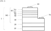
- Figure 3 shows a representative example of a semiconductor chip obtained by the method of the present invention. It will be appreciated that the semiconductor wafer has a plurality of configurations of the semiconductor chip in Figure 3 , and the layer constitution and the like are the same for the semiconductor wafer and the semiconductor chip.
- a semiconductor wafer 1 of the present invention includes an element layer 90 including an n-type layer 30, an active layer 40, and a p-type layer 60 on one surface of a sapphire substrate 10.
- the element layer has a characteristic in that a surface thereof is bent in a convex way ( Figure 2 ).
- the semiconductor wafer of the present invention has a characteristic in that the surface of the element layer 90 is bent in a convex way.
- the curvature indicating the degree of bending is 530 km -1 to 800 km -1 .
- the curvature can be measured by X-ray diffraction (XRD), a laser displacement meter, and an interference microscope.
- XRD X-ray diffraction
- the curvature is a value measured with a laser displacement meter.
- the curvature is a value obtained from the surface of the element layer 90 in the semiconductor wafer before forming an electrode.
- the curvature means a curvature of the outermost surface of the p-type layer 60
- the curvature means a curvature of the surface of the p-type contact layer 62.
- the curvature means an average value of curvatures at three or more measurement points.
- the dislocation density of the element layer 90 in the present invention is 1 ⁇ 10 8 [cm -2 ] to 1 ⁇ 10 9 [cm -2 ].
- the dislocation density is a value measured by a transmission electron microscope and is a value obtained by confirming the dislocation density of the n-type layer 30.
- the inventors of the present invention presume as follows.
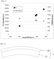
- the inventors of the present invention have found that when an n-type AlGaN layer is grown on the sapphire substrate 10 under various conditions, X-ray rocking curves of the (102) plane are about the same (700 to 800 [arcsec]; indicating that the dislocation density does not change), but the PL intensity of the n-type AlGaN layer can be increased by increasing the curvature of the obtained laminate (surface of the n-type AlGaN layer) to a certain extent (see Figure 1 ). From this result, it is suggested that if the surface of the element layer 90 can be bent to a certain extent in a convex shape, the dislocation density in the active layer or the like will not be increased, and incorporation of impurities and point defects will be suppressed. In addition, the inventors of the present invention have found that the optical output can be efficiently increased by setting the curvature of the surface of the element layer 90 to 530 km -1 to 800 km -1 , and thus complete the present invention.
- the curvature of the surface of the element layer 90 is less than 530 km -1 , the effect of improving the optical output is small. Also, if the curvature of the surface of the element layer 90, contrary to the invention, is more than 800 km -1 , the semiconductor wafer is bent too largely to be subjected to post processing such as polishing and is difficult to be used as a product. In addition, it is difficult to produce a semiconductor wafer having a curvature more than 800 km -1 . Considering improvement of optical output, handling property, productivity or the like, the curvature is preferably 600 km -1 to 800 km -1 , and more preferably 600 km -1 to 750 km -1 .
- the sapphire substrate 10 is not particularly limited, and a known substrate produced by a known method can be used.
- a thickness of the sapphire substrate 10 is not particularly limited and is usually 300 ⁇ m to 600 ⁇ m.
- the sapphire substrate 10 preferably has a (0001) plane as a growth plane (a plane on which the element layer is grown).
- the element layer 90 is formed on the sapphire substrate 10.
- the group III nitride single crystal layer particularly an Al x In y Ga z N layer having the above composition
- the optical output tends to be lowered easily.
- the optical output can be increased without changing the layer constitution by the present invention. Therefore, the present invention can exhibit an excellent effect when the element layer 90 contains Al.
- the present invention is suitable for an ultraviolet light emitting diode (wafer) having an emission peak wavelength at the ultraviolet region, specifically in a range of 200 nm to 350 nm.
- the element layer 90 may be directly formed on the sapphire substrate 10, or as shown in Figure 3 , the element layer 90 is preferably formed after the buffer layer 20 is formed. Next, the buffer layer 20 will be described.
- the semiconductor wafer 1 of the present invention when used for an ultraviolet light emitting diode, it is preferably that 0.9 ⁇ X1 ⁇ 1, 0 ⁇ Y1 ⁇ 0.1, and 0 ⁇ Z1 ⁇ 0.1, and it is most preferably that a buffer layer 20 made of AlN is adopted considering the productivity.
- a thickness of the buffer layer 20 is not particularly limited and is preferably 0.01 ⁇ m to 5 ⁇ m.
- the buffer layer 20 may be a single layer or may be a plurality of layers of two or more as described in detail below.
- the plurality of layers may be layers having different compositions or may be layers having the same composition but different growth conditions.
- the layers having the same composition but different growth conditions mean the layers that are grown while changing a ratio (V/III ratio) of the number of moles of nitrogen source gas to the number of moles of a group III raw material gas, the ratio being one of the growth conditions. Most preferred is two or more layers of AlN grown while changing the V/III.
- the buffer layer 20 may be a gradient layer whose composition continuously changes.
- the element layer 90 on the buffer layer 20. Next, each layer constituting the element layer 90 will be described.
- the n-type layer 30 is formed on the sapphire substrate 10 via the buffer layer 20 as required.
- the n-type layer 30 is a layer doped with an n-type dopant.
- the n-type layer 30 is not particularly limited, for example, it is preferable that the n-type layer 30 exhibits n-type conductivity by containing Si as a dopant in a range where the impurity concentration is 1 ⁇ 10 16 [cm -3 ] to 1 ⁇ 10 21 [cm -3 ].
- the dopant material may be a material other than Si.
- the n-type layer 30 may be a gradient layer whose composition continuously changes.
- the thickness of the n-type layer 30 is preferably 0.1 ⁇ m to 20 ⁇ m.
- the active layer 40 is formed on the n-type layer 30.
- the active layer 40 may be composed of, for example, one or more well layers and barrier layers.
- the number of wells composed of the well layers and the barrier layers may be one, or two or more. In the case of two or more, although not particularly limited, the number is preferably 10 or less considering the productivity of the nitride semiconductor light emitting device.
- the layer in contact with the n-type layer 30 may be either a well layer or a barrier layer.
- the active layer 40 is made of a well layer and a barrier layer.
- a band gap of the barrier layer is larger than that of the well layer. That is, the barrier layer is formed of an AlGaInN layer having an Al composition ratio higher than that of the well layer.
- the thickness of the barrier layer 42 is preferably 2 nm to 50 nm.
- a thickness of the well layer 41 is preferably 1 nm to 20 nm.
- the p-type layer 60 may be formed directly on the active layer 40, but the p-type layer 60 is preferably formed via the electron blocking layer 50.
- the electron blocking layer 50 suppresses leakage of a part of electrons injected from the n-type layer 30 into the active layer 40 to a p-type layer 60 side due to application of an electric field. Therefore, the electron blocking layer 50 can be substituted by a p-type clad layer 61 to be described later, but by providing the electron blocking layer 50, an Al composition of the p-type clad layer can be lowered, and a film thickness can be reduced, and as a result, a driving voltage can be reduced.
- a band gap of the electron blocking layer 50 is preferably larger than the band gap of the active layer 40 (a barrier layer having the maximum band gap in the active layer (having the maximum Al composition)) and that of a layer forming the p-type layer 60 to be described later. Therefore, the electron blocking layer 50 is preferably formed of a single crystal made of AlInGaN having an Al composition ratio higher than that of the above layers. That is, the electron blocking layer 50 is preferably formed of an AlInGaN single crystal layer having an Al composition higher than any of the other layers.
- the electron blocking layer 50 may be a gradient layer whose composition continuously changes.
- the electron blocking layer 50 may be an undoped layer or a p-type layer.
- the p-type layer contains p-type dopant such as Mg in a range where the impurity concentration is 1 ⁇ 10 16 [cm -3 ] to 1 ⁇ 10 21 [cm -3 ].
- a thickness of the electron blocking layer 50 is preferably 1 nm to 50 nm.
- the p-type layer 60 is formed on the active layer 40 or on the electron blocking layer 50 provided as required.
- the p-type layer 60 is not particularly limited and is preferably made of the p-type clad layer 61 and the p-type contact layer 62 on which a p-electrode 80 is formed.
- the p-type clad layer 61 contains Mg as a dopant in a range where the impurity concentration is 1 ⁇ 10 16 [cm -3 ] to 1 ⁇ 10 21 [cm -3 ].
- a thickness of the p-type clad layer 61 is not particularly limited and is preferably 1 nm to 1 ⁇ m.
- the p-type contact layer 62 in contact with the p-electrode is preferably provided on the p-type clad layer 61.
- the p-type contact layer 62 By forming the p-type contact layer 62, ohmic contact with the p-electrode 80 can be easily realized and reduction in contact resistance can be easily realized.
- the p-type contact layer 62 is formed of a single crystal made of GaN.
- the p-type contact layer 62 contains Mg a dopant in a range where the impurity concentration is 1 ⁇ 10 16 [cm -3 ] to 1 ⁇ 10 21 [cm -3 ].
- a thickness of the p-type contact layer 62 is not particularly limited and is preferably 1 nm to 1000 nm.
- the n-electrode 70 is formed on the exposed surface of the n-type layer 30.
- Materials used for the n-electrode 70 can be selected from various known materials. For example, Ti, Al, Rh, Cr, V, In, Ni, Pt, Au, or the like can be used. Among these, it is preferable to use Ti, Al, Rh, Cr, V, Ni, and Au.
- These negative electrodes may have a single layer or multi-layer structure having a layer containing an alloy or an oxide of these metals, and a preferred combination is Ti/Al/Au from the viewpoint of ohmic property and reflectance.
- a thickness thereof is not particularly limited and is preferably 2 nm or more considering the stability of production, and an upper limit thereof is 2 ⁇ m.
- the p-electrode 80 is formed on the p-type contact layer 62.
- the p-electrode 80 preferably has a high transparency to ultraviolet light. Specifically, the transmittance thereof is 60% or more, and preferably 70% or more, to the light of 265 nm. Although not particularly limited, an upper limit thereof is preferably 100%, and industrially preferably 90% or more.
- Metal materials used for the p-electrode 80 can be selected from various known materials. For example, Ni, Cr, Au, Mg, Zn, Pd or the like can be used.
- the light-transmissive positive electrode may be a single layer or multi-layer structure having a layer containing an alloy or an oxide of these metals and a preferred combination is Ni/Au.
- the film thickness is preferably as small as possible. Specifically, the film thickness is 10 nm or less, and more preferably 5 nm or less, and a lower limit thereof is 0.5 nm. When it is not necessary for the p-electrode 80 to have a light-transmission property, the above is not the limit and the film thickness may be thick. Specifically, the film thickness is 500 nm or less, and more preferably 100 nm or less, and a lower limit thereof is 0.5 nm.
- a semiconductor light emitting device having an n-electrode and a p-electrode on a semiconductor wafer is used, and the semiconductor wafer is cut to obtain a semiconductor chip.
- a preferred method for producing the semiconductor wafer 1 of the present invention will be described.
- the semiconductor wafer 1 is produced by forming the element layer 90 on the sapphire substrate 10.
- the sapphire substrate 10 to be used preferably has (0001) plane on which the element layer is grown.
- the (0001) plane may have an off angle, and it is preferable to form an element layer on the (0001) plane inclined at 0° to 5°. Further, the (0001) plane is preferably inclined to an m-axis direction.
- the (0001) plane is smooth, and it is preferable that the (0001) plane has a surface roughness of about 0.2 nm or less. It is preferable that a bending amount (radius of curvature) of the sapphire substrate 10 before growing the element layer 90 is 10 m or more. An upper limit of the radius of curvature is not particularly limited.
- the element layer 90 is formed on the sapphire substrate 10.
- Conditions for producing the semiconductor wafer of the present invention are not particularly limited, and the growth is preferably performed by a metal organic chemical vapor deposition (MOCVD) method.
- MOCVD metal organic chemical vapor deposition
- the amount of oxygen introduced cannot be unconditionally limited since the optimum value varies depending on the capacity, shape, etc. of each apparatus.
- oxygen air
- the sapphire substrate 10 is set in the MOCVD apparatus, and thermal cleaning or the like may be performed by a known method, thereafter the buffer layer 20 or the element layer 90 is formed.
- the element layer 90 can also be bent in a convex way by growing the buffer layer provided as required and the n-type layer under a pressure. Specifically, it is preferable to grow the above layers on the sapphire substrate 10 under a pressure of 50 Torr to 200 Torr. Although the reason is unclear, it is thought that at the early stage of growth, the growth of the layer to be formed is influenced by the pressure, and thereby the finally obtained element layer 90 can be bent in a convex way.
- the element layer 90 may be directly formed on the (0001) plane of the sapphire substrate 10 but is preferably formed via the buffer layer 20, as described above. Next, the growth of the buffer layer 20 will be described.
- the preferred composition is as described above.
- the growth is preferably performed by a metal organic chemical vapor deposition (MOCVD) method.
- the oxygen introduction method and/or the growth method under a pressure of 50 Torr to 200 Torr, and to control the V/III ratio under the growth conditions of the buffer layer 20. That is, it is preferable to control the ratio (V/III ratio) of the number of moles of the nitrogen source gas to the number of moles of the group III raw material gas.
- the curvature after growth becomes high when the V/III ratio high, and the more the element layer 90 is bent convexly.
- the range of the V/III ratio under the production conditions is not particularly limited and is preferably 50 to 10000. It is presumed that, when the V/III ratio is within the above range, nucleation sizes are different at the early stage of growth, and thus the subsequent association process of growth nuclei is different, so that a bent semiconductor wafer can be obtained.
- the buffer layer 20 in at least two stages.
- an AlN single crystal layer can be grown in multiple stages with the V/III ratio in a range of 50 to 2000.
- the buffer layer (second buffer layer) by two stages including a second growth step, after the first growth step.
- a thickness of the second buffer layer is larger than that of the first buffer layer.
- the thickness of the first buffer layer is preferably 0.004 ⁇ m to 0.5 ⁇ m
- the thickness of the second buffer layer is preferably 0.006 ⁇ m to 4.5 ⁇ m.
- the nitrogen source gas for example, ammonia
- the group III raw material gas for example, trimethylaluminum gas, trimethylgallium gas, and trimethylindium gas
- the nitrogen source gas for example, ammonia
- the group III raw material gas for example, trimethylaluminum gas, trimethylgallium gas, and trimethylindium gas
- the method for growing the n-type layer 30 is also not particularly limited, and it is preferable to grow the n-type layer 30 by the MOCVD method.
- the n-type layer 30 is directly laminated on the sapphire substrate 10.
- a condition for growing the n-type layer 30 a known method can be adopted.
- the growth conditions of the n-type layer 30 on the sapphire substrate 10 can be the same as those of the buffer layer 20.
- the n-type layer 30 may be grown by supplying an n-type dopant in addition to the Al and Ga raw material gas and ammonia.
- an n-type dopant such as Si and O can be used as an element of the n-type dopant, Si is preferably used from the viewpoint of easy control or the like.
- the Si raw material monosilane (SiH 4 ), tetraethylsilane (TESi) or the like can be used.
- a growth temperature at the time of growing the n-type layer 30 is not particularly limited, and is preferably 900°C to 1100°C.
- a growth rate is preferably 0.1 ⁇ m/h to 2.0 ⁇ m/h.
- the V/III ratio is not particularly limited, and is preferably 1500 to 10000, and more preferably 2000 to 5000, in order to satisfy the growth rate in the above temperature range.
- the active layer 40 can also be grown by the MOCVD method so as to satisfy a desired composition.
- a condition for forming the active layer 40 a known method can be adopted.
- a growth temperature of the active layer 40 is not particularly limited and is preferably more than 1000°C to 1200°C or lower, and preferably more than 1020°C to 1100°C or lower.
- the V/III ratio at growing the active layer 40 is not particularly limited, and is preferably 1000 to 10000, and more preferably 1500 to 8000.
- a growth rate of the active layer 40 is preferably 0.05 ⁇ m/h to 1.0 ⁇ m/h, and more preferably 0.1 ⁇ m/h to 0.8 ⁇ m/h.
- the growth rate of the active layer is preferably in the range of 0.05 ⁇ m/h to 1.0 ⁇ m/h for all layers of the quantum well layer and the barrier layer.
- the electron blocking layer 50 formed as required can also be grown by the MOCVD method. As for a condition for forming the electron blocking layer 50, a known method can be adopted.
- a growth temperature of the electron blocking layer 50 is not particularly limited and is preferably higher than 1020°C to 1200°C or lower, and more preferably higher than 1050°C to 1150°C or lower.
- a growth rate is preferably 0.1 ⁇ m/h to 1.0 ⁇ m/h, and more preferably 0.1 ⁇ m/h to 0.8 ⁇ m/h.
- the V/III ratio is not particularly limited, and is preferably in a range of 2000 to 20000, and more preferably in a range of 2500 to 15000.
- the electron blocking layer 50 can also be a p-type by adding a p-type impurity.
- the electron blocking layer 50 is produced by supplying a p-type impurity in addition to the Al and Ga raw material gas and ammonia.
- a p-type impurity a known material can be used without limitation, and Mg is preferably used considering the activation energy of the p-type impurity or the like.
- the p-type clad layer 61 can also be grown by the MOCVD method. Specifically, the p-type clad layer 61 is produced by supplying a p-type impurity in addition to the Al and Ga raw material gas and ammonia.
- a known material can be used without limitation, and Mg is preferably used considering the activation energy of the p-type impurity or the like.
- a condition for forming the p-type clad layer 61 a known method can be adopted.
- the p-type contact layer 62 can also be grown by the MOCVD method, and the same impurity as of the p-type clad layer 61 can be added.
- a growth temperature is not particularly limited, and is preferably 1000°C to 1080°C, and more preferably 1020°C to 1050°C.
- a growth rate is also not particularly limited, and is preferably 0.03 ⁇ m/h to 1.0 ⁇ m/h.
- the V/III ratio is preferably set within a range of 2000 to 15000, more preferably 4000 to 12000, and most preferably 6000 to 10000.
- the n-electrode 70 is formed on the exposed surface of the n-type layer 30.
- the exposed surface of the n-type layer 30 is formed by means such as etching.
- Preferred etching methods include dry etching such as reactive ion etching and inductively coupled plasma etching.
- the exposed surface is preferably subject to surface treatment with an acid or alkaline solution.
- patterning of the n-electrode can be performed using a lift-off method.
- Examples of a method for depositing a metal forming the n-electrode include vacuum evaporation, sputtering, chemical vapor deposition or the like, and the vacuum evaporation is preferred in order to eliminate impurities in the electrode metal.
- the material used for the n-electrode is as described above.
- Patterning of the p-electrode 80 is preferably performed using a lift-off method.
- the metal material used for the p-electrode 80 is as described above. Examples of a method for depositing a metal of the p-electrode 80 include vacuum evaporation, sputtering, chemical vapor deposition or the like, and the vacuum evaporation is preferred in order to eliminate impurities in the electrode metal.
- a sapphire C plane ((0001) plane) single crystal substrate ( ⁇ 2 inches ⁇ thickness 330 ⁇ m) was used as a crystal growth substrate. 5 minutes after opening an MOCVD apparatus, the sapphire substrate was placed on a susceptor in the MOCVD apparatus, and then the sapphire substrate was heated to 1230°C for 10 minutes while flowing hydrogen at a flow rate of 13 slm (heat treatment step).
- An AlN single crystal layer was formed as a first buffer layer in a thickness of 0.1 ⁇ m under conditions of a total flow rate of 10 slm and a pressure of 25 Torr (a first growth step: growth of the first buffer layer).
- the temperature of the substrate on which the AlN single crystal layer of the first buffer layer was deposited on the sapphire substrate was set to 1180°C
- the flow rate of trimethylaluminum was set to 26 ⁇ mol/min
- the flow rate of ammonia was set to 0.5 slm.
- the flow rate of the raw material gas was adjusted such that the V/III ratio at this time was 850.
- An AlN single crystal layer of 1.9 ⁇ m was formed as a second buffer layer under conditions of a total flow rate of 10 slm and a pressure of 25 Torr (second growth step; growth of the second buffer layer).
- an n-type layer 30 having an Al composition of 70%, a Ga composition of 30% and an In composition of 0% was formed in a thickness of 2.0 ⁇ m. Meanwhile, the pressure in the apparatus was 38 Torr. At this time, a half-value width of an X-ray rocking curve of (102) plane was 700 arcsec.
- the substrate temperature was set to 1060°C, and after the temperature was constant, an Al 0.7 Ga 0.3 N barrier layer of 7 nm was formed under the same growth conditions as those for growing the n-type layer, except that the flow rate of tetraethylsilane was 0.002 ⁇ mol/min, the flow rate of trimethylaluminum was 13.3 ⁇ mol/min, and the flow rate of trimethylgallium was 11.2 ⁇ mol/min.
- an Al 0.5 Ga 0.5 N well layer of 2 nm was formed under the same conditions as those for growing the n-type layer, except that the flow rate of trimethylgallium was 40 ⁇ mol/min, and the flow rate of trimethylaluminum was 2 ⁇ mol/min.
- the growth of the well layer and the barrier layer was repeated for three times to form a triple quantum well layer. Meanwhile, the pressure in the apparatus was 38 Torr.
- the supply of trimethylgallium and tetraethylsilane was stopped and the substrate temperature was set to 1100°C.
- an electron blocking layer 50 of 20 nm was formed under the same conditions as those for growing the n-type layer, except that bicyclopentadienyl magnesium was supplied at 1.0 ⁇ mol/min.
- the Al composition is 100%. Meanwhile, the pressure in the apparatus was 38 Torr.
- a p-type clad layer 61 of 35 nm was formed under the same conditions as those for growing the n-type layer, except that bicyclopentadienyl magnesium was supplied at 1.0 ⁇ mol/min.
- the Al composition was 70%
- the Ga composition was 30%
- the In composition was 0%.
- the pressure in the apparatus was 38 Torr.
- the substrate temperature was changed to 1030°C and the pressure was changed to 150 Torr, and thereafter a GaN layer of 240 nm was formed as the p-type contact layer 62 under conditions of a flow rate of trimethylgallium of 36.0 ⁇ mol/min, a flow rate of ammonia of 2.5 slm, a flow rate of bicyclopentadienyl magnesium of 0.66 ⁇ mol/min, and a flow rate of carrier gas (hydrogen) of 3.5 slm. Meanwhile, the pressure in the apparatus was 150 Torr. Accordingly, a semiconductor wafer was produced.
- the curvature of the surface of the element layer 90 (p-type contact layer 62) of the obtained semiconductor wafer was measured by a laser displacement meter method.
- the curvature of the semiconductor wafer was 543 km -1 , and the results were shown in Table 1.
- the obtained semiconductor wafer was subject to heat treatment in a nitrogen atmosphere at 900°C for 20 minutes. Thereafter, a predetermined resist pattern was formed on the surface of the p-type contact layer 62 by photolithography, and a window portion without forming a resist pattern was etched by reactive ion etching until the surface of the n-type layer 30 was exposed. Thereafter, a Ti (20 nm) / Al (200 nm) /Au (5 nm) electrode (negative electrode) was formed as the n-electrode 70 on the surface of the n-type layer 30 by a vacuum evaporation method, and heat treatment was performed under a condition of 810°C for 1 minute in a nitrogen atmosphere.
- an Ni (20 nm) / Au (50 nm) electrode (positive electrode) was formed as the p-electrode 80 on the surface of the p-type contact layer 62 by a vacuum evaporation method, and thereafter heat treatment was performed in an oxygen atmosphere at 550°C for 3 minutes to produce a nitride semiconductor light emitting device.
- the optical output and the wavelength at a driving current of 30 mA were 0.44 mW and 272 nm.
- the results were summarized in Table 1.
- a semiconductor wafer and a semiconductor light emitting device were produced under the same conditions as in Example 1, except that the flow rate of trimethylaluminum when forming the buffer layer 20 (the first growth step) was 13.1 ⁇ mol/min, and the V/III ratio at that time was 5100.
- the optical output and the wavelength at a driving current of 30 mA were 0.87 mW and 269 nm, and the curvature of the semiconductor wafer was 613 km -1 . The results were shown in Table 1.
- a semiconductor wafer and a semiconductor light emitting device were produced under the same conditions as in Example 1, except that the flow rate of trimethylaluminum when forming the buffer layer 20 (the first growth step) was 6.6 ⁇ mol/min, and the V/III ratio at that time was 6800.
- the optical output and the wavelength at a driving current of 30 mA were 1.48 mW and 267 nm, and the curvature of the semiconductor wafer was 701 km -1 . The results were shown in Table 1.
- the buffer layer 20 was grown to 2 ⁇ m under the conditions same as the second growth step of Example 1, except that the opening time of MOCVD apparatus before introduction of the sapphire substrate was 1 minute and the first growth step was not performed.
- n-type Layer 30 and Layers after n-type Layer 30 Growth conditions for the n-type Layer 30 and the layers after the n-type layer 30 are the same as those in Example 1, then a semiconductor wafer and a semiconductor light emitting device were produced. Further, the half-value width in the (102) plane of the X-ray rocking curve when the n-type layer was formed under this condition was measured.
Landscapes
- Led Devices (AREA)
- Crystals, And After-Treatments Of Crystals (AREA)
- Chemical & Material Sciences (AREA)
- Crystallography & Structural Chemistry (AREA)
Claims (8)
- Halbleiterwafer (1) mit einer Elementschicht (90), die eine Schicht vom n-Typ (30), eine aktive Schicht (40) und eine Schicht vom p-Typ (60) auf einer Oberfläche eines Saphirsubstrats (10) aufweist,wobei eine Oberfläche der Elementschicht (90) konvex gebogen ist,dadurch gekennzeichnet, dass eine Krümmung der Oberfläche der Elementschicht (90) 530 km-1 bis 800 km-1 beträgt, unddie Elementschicht (90) Gruppe-III-Nitrideinkristallschichten aufweist, die aus AlGaInN-Schichten hergestellt sind, die eine durch AlxInyGazN dargestellte Zusammensetzung erfüllen, wobei x, y und z rationale Zahlen sind, die 0,3 ≤ x ≤ 1,0, 0 ≤ y ≤ 0,7 und 0 ≤ z ≤ 0,7 erfüllen, und x + y + z = 1,0 ist.
- Halbleiterwafer (1) nach Anspruch 1, wobei eine Ebene des Saphirsubstrats (10), auf der die Elementschicht (90) ausgebildet ist, eine (0001)-Ebene ist.
- Halbleiterwafer (1) nach Anspruch 1 oder 2, wobei eine Pufferschicht (20), die aus AlxInyGazN hergestellt ist, wobei x, y und z rationale Zahlen sind, die 0,8 ≤ x ≤ 1,0, 0 ≤ y ≤ 0,2 und 0 ≤ z ≤ 0,2 erfüllen, und x + y + z = 1,0 ist, zwischen der einen Oberfläche des Saphirsubstrats (10) und der Elementschicht (90) enthalten ist.
- Halbleiterwafer (1) nach Anspruch 3, wobei die Pufferschicht (20) mindestens zwei Schichten einer ersten Pufferschicht und einer zweiten Pufferschicht aufweist.
- Halbleiterwafer (1) mit einer Elementschaltung, der eine n-Elektrode (70) auf der Schicht vom n-Typ (30) und eine p-Elektrode (80) auf der Schicht vom p-Typ (60) des Halbleiterwafers (1) nach einem der Ansprüche 1 bis 4 aufweist.
- Verfahren zum Herstellen einer lichtemittierenden Halbleitervorrichtung, das einen Schritt des Schneidens des Halbleiterwafers mit einer Elementschaltung nach Anspruch 5 in Halbleiterchips aufweist.
- Verfahren zum Herstellen einer lichtemittierenden Halbleitervorrichtung nach Anspruch 6, wobei eine Emissionsspitzenwellenlänge der lichtemittierenden Halbleitervorrichtung in einem Ultraviolettbereich liegt.
- Verfahren zum Herstellen einer lichtemittierenden Halbleitervorrichtung nach Anspruch 7, wobei die Emissionsspitzenwellenlänge der lichtemittierenden Halbleitervorrichtung in einem Bereich von 200 nm bis 350 nm liegt.
Applications Claiming Priority (2)
| Application Number | Priority Date | Filing Date | Title |
|---|---|---|---|
| JP2016077829 | 2016-04-08 | ||
| PCT/JP2017/014519 WO2017175860A1 (ja) | 2016-04-08 | 2017-04-07 | 半導体ウェハ |
Publications (3)
| Publication Number | Publication Date |
|---|---|
| EP3442038A1 EP3442038A1 (de) | 2019-02-13 |
| EP3442038A4 EP3442038A4 (de) | 2019-11-06 |
| EP3442038B1 true EP3442038B1 (de) | 2025-01-01 |
Family
ID=60001174
Family Applications (1)
| Application Number | Title | Priority Date | Filing Date |
|---|---|---|---|
| EP17779237.1A Active EP3442038B1 (de) | 2016-04-08 | 2017-04-07 | Halbleiter-wafer |
Country Status (6)
| Country | Link |
|---|---|
| US (1) | US10770621B2 (de) |
| EP (1) | EP3442038B1 (de) |
| JP (1) | JP6830098B2 (de) |
| KR (1) | KR102112249B1 (de) |
| CN (1) | CN109075224B (de) |
| WO (1) | WO2017175860A1 (de) |
Families Citing this family (8)
| Publication number | Priority date | Publication date | Assignee | Title |
|---|---|---|---|---|
| US10937928B2 (en) | 2017-11-09 | 2021-03-02 | Asahi Kasei Kabushiki Kaisha | Nitride semiconductor element, nitride semiconductor light emitting element, ultraviolet light emitting element |
| JP7049823B2 (ja) * | 2017-12-18 | 2022-04-07 | 旭化成株式会社 | 窒化物半導体発光素子 |
| FR3102302B1 (fr) * | 2019-10-17 | 2023-08-25 | Commissariat Energie Atomique | DIODE ELECTROLUMINESCENTE COMPRENANT UN SEMI-CONDUCTEUR A BASE D’AlN DOPE P PAR DES ATOMES DE MAGNESIUM |
| KR102315911B1 (ko) * | 2020-01-08 | 2021-10-22 | 웨이브로드 주식회사 | 반도체 발광소자 및 이를 제조하는 방법 |
| JP6814902B1 (ja) * | 2020-04-24 | 2021-01-20 | 日機装株式会社 | 半導体発光素子および半導体発光素子の製造方法 |
| EP4292123A4 (de) * | 2021-02-26 | 2025-03-05 | The Regents of University of California | Verfahren zur verbesserung der leistungen von durch metallorganische chemische aufdampfung gezüchteten tunnelübergängen |
| JP7340047B2 (ja) * | 2022-01-25 | 2023-09-06 | 日機装株式会社 | 窒化物半導体発光素子の製造方法 |
| JP2024058791A (ja) | 2022-10-17 | 2024-04-30 | スタンレー電気株式会社 | 垂直共振器型発光素子 |
Family Cites Families (18)
| Publication number | Priority date | Publication date | Assignee | Title |
|---|---|---|---|---|
| US6252261B1 (en) | 1998-09-30 | 2001-06-26 | Nec Corporation | GaN crystal film, a group III element nitride semiconductor wafer and a manufacturing process therefor |
| JP2000349338A (ja) | 1998-09-30 | 2000-12-15 | Nec Corp | GaN結晶膜、III族元素窒化物半導体ウェーハ及びその製造方法 |
| JP4595207B2 (ja) * | 2001-01-29 | 2010-12-08 | パナソニック株式会社 | 窒化物半導体基板の製造方法 |
| US6946788B2 (en) * | 2001-05-29 | 2005-09-20 | Toyoda Gosei Co., Ltd. | Light-emitting element |
| JP2003063897A (ja) * | 2001-08-28 | 2003-03-05 | Sony Corp | 窒化物系iii−v族化合物半導体基板およびその製造方法ならびに半導体発光素子の製造方法ならびに半導体装置の製造方法 |
| JP2005116785A (ja) | 2003-10-08 | 2005-04-28 | Nippon Telegr & Teleph Corp <Ntt> | 半導体材料薄膜の成長法 |
| KR101094403B1 (ko) * | 2004-01-29 | 2011-12-15 | 삼성코닝정밀소재 주식회사 | 휨이 감소된 사파이어/질화갈륨 적층체 |
| WO2005099057A1 (ja) * | 2004-03-31 | 2005-10-20 | Nec Corporation | 窒化物半導体発光素子用ウエハとその製造方法およびそのウエハから得られた窒化物半導体発光素子 |
| WO2011065745A2 (ko) * | 2009-11-27 | 2011-06-03 | 서울옵토디바이스주식회사 | 발광다이오드 패키지 |
| CN102792420B (zh) * | 2010-03-05 | 2016-05-04 | 并木精密宝石株式会社 | 单晶衬底、单晶衬底的制造方法、带多层膜的单晶衬底的制造方法以及元件制造方法 |
| JP2012009695A (ja) * | 2010-06-25 | 2012-01-12 | Showa Denko Kk | 半導体発光素子の製造方法、半導体発光素子、電子機器及び機械装置 |
| WO2012150647A1 (ja) * | 2011-05-02 | 2012-11-08 | パナソニック株式会社 | スーパールミネッセントダイオード |
| CN106968014B (zh) | 2012-03-21 | 2019-06-04 | 弗赖贝格化合物原料有限公司 | 用于制备iii-n单晶的方法以及iii-n单晶 |
| KR20130107791A (ko) * | 2012-03-23 | 2013-10-02 | 엘지이노텍 주식회사 | 발광소자 |
| JP6024533B2 (ja) * | 2012-03-28 | 2016-11-16 | 日亜化学工業株式会社 | サファイア基板及びその製造方法並びに窒化物半導体発光素子 |
| US20160265140A1 (en) * | 2012-10-31 | 2016-09-15 | Namiki Seimitsu Houseki Kabushiki Kaisha | Single crystal substrate, manufacturing method for single crystal substrate, manufacturing method for single crystal substrate with multilayer film, and element manufacturing method |
| CN105102695B (zh) * | 2013-12-18 | 2018-06-12 | 日本碍子株式会社 | 复合基板和功能元件 |
| CN105448852A (zh) * | 2014-08-27 | 2016-03-30 | 群创光电股份有限公司 | 曲面电子装置 |
-
2017
- 2017-04-07 KR KR1020187028964A patent/KR102112249B1/ko active Active
- 2017-04-07 US US16/092,007 patent/US10770621B2/en active Active
- 2017-04-07 WO PCT/JP2017/014519 patent/WO2017175860A1/ja not_active Ceased
- 2017-04-07 CN CN201780021775.9A patent/CN109075224B/zh active Active
- 2017-04-07 JP JP2018510677A patent/JP6830098B2/ja active Active
- 2017-04-07 EP EP17779237.1A patent/EP3442038B1/de active Active
Also Published As
| Publication number | Publication date |
|---|---|
| WO2017175860A1 (ja) | 2017-10-12 |
| CN109075224A (zh) | 2018-12-21 |
| KR102112249B1 (ko) | 2020-05-18 |
| US10770621B2 (en) | 2020-09-08 |
| CN109075224B (zh) | 2021-10-26 |
| EP3442038A4 (de) | 2019-11-06 |
| KR20180123084A (ko) | 2018-11-14 |
| JP6830098B2 (ja) | 2021-02-17 |
| US20190115499A1 (en) | 2019-04-18 |
| JPWO2017175860A1 (ja) | 2019-02-14 |
| EP3442038A1 (de) | 2019-02-13 |
Similar Documents
| Publication | Publication Date | Title |
|---|---|---|
| EP3442038B1 (de) | Halbleiter-wafer | |
| EP2383846B1 (de) | Lichtemissionsvorrichtung und Herstellungsverfahren dafür | |
| EP3331035B1 (de) | Lichtemittierendes gruppe-iii-nitrid-halbleiterbauelement und herstellungsverfahren dafür | |
| KR101066135B1 (ko) | Ⅲ족 질화물 화합물 반도체 적층 구조체 | |
| US8513694B2 (en) | Nitride semiconductor device and manufacturing method of the device | |
| JP4191227B2 (ja) | Iii族窒化物半導体発光素子の製造方法及びiii族窒化物半導体発光素子並びにランプ | |
| EP3425684B1 (de) | Senkrechte uv-lichtemittierende diode | |
| EP2352182A1 (de) | Verfahren zur herstellung eines lichtemittierenden nitridhalbleiterelements und verfahren zur herstellung eines epitaktischen wafers | |
| JP2001160627A (ja) | Iii族窒化物系化合物半導体発光素子 | |
| EP2164115A1 (de) | Nitridhalbleiter-leuchtelement und verfahren zur herstellung eines nitridhalbleiters | |
| JPWO2010032423A1 (ja) | Iii族窒化物半導体発光素子の製造方法、iii族窒化物半導体発光素子並びにランプ、iii族窒化物半導体発光素子ウエーハの発光波長分布のばらつき低減方法 | |
| US20160111592A1 (en) | Light emitting devices and methods of manufacturing the same | |
| JP2001160627A5 (de) | ||
| EP3336908B1 (de) | Halbleiter-mehrschichtfilmspiegel, lichtemittierendes bauelement mit vertikalem hohlraum mit dem spiegel und verfahren zur herstellung des spiegels und des elements | |
| KR101071450B1 (ko) | Ⅲ족 질화물 반도체층의 제조 방법 및 ⅲ족 질화물 반도체 발광 소자, 및 램프 | |
| US7951617B2 (en) | Group III nitride semiconductor stacked structure and production method thereof | |
| US20070284599A1 (en) | Process for producing group III nitride semiconductor stacked structure | |
| JP2007103774A (ja) | Iii族窒化物半導体積層構造体およびその製造方法 | |
| WO2009142265A1 (ja) | Iii族窒化物半導体発光素子及びその製造方法、並びにランプ | |
| JP2003347660A (ja) | 窒化物半導体装置の製造方法 | |
| JP2005085932A (ja) | 発光ダイオード及びその製造方法 | |
| KR100742986B1 (ko) | 컴플라이언트 기판을 갖는 질화갈륨계 화합물 반도체 소자의 제조 방법 | |
| JP5105738B2 (ja) | 窒化ガリウム系化合物半導体積層物の製造方法 | |
| JP2008294449A (ja) | Iii族窒化物半導体発光素子の製造方法及びiii族窒化物半導体発光素子並びにランプ | |
| CN117293241B (zh) | 发光二极管外延片及其制备方法、发光二极管 |
Legal Events
| Date | Code | Title | Description |
|---|---|---|---|
| STAA | Information on the status of an ep patent application or granted ep patent |
Free format text: STATUS: THE INTERNATIONAL PUBLICATION HAS BEEN MADE |
|
| PUAI | Public reference made under article 153(3) epc to a published international application that has entered the european phase |
Free format text: ORIGINAL CODE: 0009012 |
|
| STAA | Information on the status of an ep patent application or granted ep patent |
Free format text: STATUS: REQUEST FOR EXAMINATION WAS MADE |
|
| 17P | Request for examination filed |
Effective date: 20181008 |
|
| AK | Designated contracting states |
Kind code of ref document: A1 Designated state(s): AL AT BE BG CH CY CZ DE DK EE ES FI FR GB GR HR HU IE IS IT LI LT LU LV MC MK MT NL NO PL PT RO RS SE SI SK SM TR |
|
| AX | Request for extension of the european patent |
Extension state: BA ME |
|
| DAV | Request for validation of the european patent (deleted) | ||
| DAX | Request for extension of the european patent (deleted) | ||
| A4 | Supplementary search report drawn up and despatched |
Effective date: 20191007 |
|
| RIC1 | Information provided on ipc code assigned before grant |
Ipc: H01L 33/32 20100101ALI20190930BHEP Ipc: H01L 33/24 20100101ALI20190930BHEP Ipc: H01L 33/20 20100101AFI20190930BHEP Ipc: H01L 21/02 20060101ALN20190930BHEP Ipc: H01L 33/00 20100101ALN20190930BHEP |
|
| STAA | Information on the status of an ep patent application or granted ep patent |
Free format text: STATUS: EXAMINATION IS IN PROGRESS |
|
| 17Q | First examination report despatched |
Effective date: 20210517 |
|
| GRAP | Despatch of communication of intention to grant a patent |
Free format text: ORIGINAL CODE: EPIDOSNIGR1 |
|
| STAA | Information on the status of an ep patent application or granted ep patent |
Free format text: STATUS: GRANT OF PATENT IS INTENDED |
|
| RIC1 | Information provided on ipc code assigned before grant |
Ipc: H01L 21/02 20060101ALN20240918BHEP Ipc: H01L 33/00 20100101ALN20240918BHEP Ipc: H01L 33/24 20100101ALI20240918BHEP Ipc: H01L 33/32 20100101ALI20240918BHEP Ipc: H01L 33/20 20100101AFI20240918BHEP |
|
| RIC1 | Information provided on ipc code assigned before grant |
Ipc: H01L 21/02 20060101ALN20240924BHEP Ipc: H01L 33/00 20100101ALN20240924BHEP Ipc: H01L 33/24 20100101ALI20240924BHEP Ipc: H01L 33/32 20100101ALI20240924BHEP Ipc: H01L 33/20 20100101AFI20240924BHEP |
|
| INTG | Intention to grant announced |
Effective date: 20241004 |
|
| GRAS | Grant fee paid |
Free format text: ORIGINAL CODE: EPIDOSNIGR3 |
|
| GRAA | (expected) grant |
Free format text: ORIGINAL CODE: 0009210 |
|
| STAA | Information on the status of an ep patent application or granted ep patent |
Free format text: STATUS: THE PATENT HAS BEEN GRANTED |
|
| AK | Designated contracting states |
Kind code of ref document: B1 Designated state(s): AL AT BE BG CH CY CZ DE DK EE ES FI FR GB GR HR HU IE IS IT LI LT LU LV MC MK MT NL NO PL PT RO RS SE SI SK SM TR |
|
| REG | Reference to a national code |
Ref country code: GB Ref legal event code: FG4D |
|
| REG | Reference to a national code |
Ref country code: CH Ref legal event code: EP |
|
| REG | Reference to a national code |
Ref country code: DE Ref legal event code: R096 Ref document number: 602017087091 Country of ref document: DE |
|
| REG | Reference to a national code |
Ref country code: IE Ref legal event code: FG4D |
|
| REG | Reference to a national code |
Ref country code: LT Ref legal event code: MG9D |
|
| REG | Reference to a national code |
Ref country code: NL Ref legal event code: MP Effective date: 20250101 |
|
| REG | Reference to a national code |
Ref country code: AT Ref legal event code: MK05 Ref document number: 1757228 Country of ref document: AT Kind code of ref document: T Effective date: 20250101 |
|
| PG25 | Lapsed in a contracting state [announced via postgrant information from national office to epo] |
Ref country code: NL Free format text: LAPSE BECAUSE OF FAILURE TO SUBMIT A TRANSLATION OF THE DESCRIPTION OR TO PAY THE FEE WITHIN THE PRESCRIBED TIME-LIMIT Effective date: 20250101 |
|
| PG25 | Lapsed in a contracting state [announced via postgrant information from national office to epo] |
Ref country code: FI Free format text: LAPSE BECAUSE OF FAILURE TO SUBMIT A TRANSLATION OF THE DESCRIPTION OR TO PAY THE FEE WITHIN THE PRESCRIBED TIME-LIMIT Effective date: 20250101 |
|
| PG25 | Lapsed in a contracting state [announced via postgrant information from national office to epo] |
Ref country code: PL Free format text: LAPSE BECAUSE OF FAILURE TO SUBMIT A TRANSLATION OF THE DESCRIPTION OR TO PAY THE FEE WITHIN THE PRESCRIBED TIME-LIMIT Effective date: 20250101 |
|
| PGFP | Annual fee paid to national office [announced via postgrant information from national office to epo] |
Ref country code: DE Payment date: 20250401 Year of fee payment: 9 |
|
| PG25 | Lapsed in a contracting state [announced via postgrant information from national office to epo] |
Ref country code: ES Free format text: LAPSE BECAUSE OF FAILURE TO SUBMIT A TRANSLATION OF THE DESCRIPTION OR TO PAY THE FEE WITHIN THE PRESCRIBED TIME-LIMIT Effective date: 20250101 |
|
| PG25 | Lapsed in a contracting state [announced via postgrant information from national office to epo] |
Ref country code: NO Free format text: LAPSE BECAUSE OF FAILURE TO SUBMIT A TRANSLATION OF THE DESCRIPTION OR TO PAY THE FEE WITHIN THE PRESCRIBED TIME-LIMIT Effective date: 20250401 Ref country code: IS Free format text: LAPSE BECAUSE OF FAILURE TO SUBMIT A TRANSLATION OF THE DESCRIPTION OR TO PAY THE FEE WITHIN THE PRESCRIBED TIME-LIMIT Effective date: 20250501 |
|
| PG25 | Lapsed in a contracting state [announced via postgrant information from national office to epo] |
Ref country code: HR Free format text: LAPSE BECAUSE OF FAILURE TO SUBMIT A TRANSLATION OF THE DESCRIPTION OR TO PAY THE FEE WITHIN THE PRESCRIBED TIME-LIMIT Effective date: 20250101 |
|
| PG25 | Lapsed in a contracting state [announced via postgrant information from national office to epo] |
Ref country code: LV Free format text: LAPSE BECAUSE OF FAILURE TO SUBMIT A TRANSLATION OF THE DESCRIPTION OR TO PAY THE FEE WITHIN THE PRESCRIBED TIME-LIMIT Effective date: 20250101 Ref country code: PT Free format text: LAPSE BECAUSE OF FAILURE TO SUBMIT A TRANSLATION OF THE DESCRIPTION OR TO PAY THE FEE WITHIN THE PRESCRIBED TIME-LIMIT Effective date: 20250502 |
|
| PG25 | Lapsed in a contracting state [announced via postgrant information from national office to epo] |
Ref country code: BG Free format text: LAPSE BECAUSE OF FAILURE TO SUBMIT A TRANSLATION OF THE DESCRIPTION OR TO PAY THE FEE WITHIN THE PRESCRIBED TIME-LIMIT Effective date: 20250101 Ref country code: GR Free format text: LAPSE BECAUSE OF FAILURE TO SUBMIT A TRANSLATION OF THE DESCRIPTION OR TO PAY THE FEE WITHIN THE PRESCRIBED TIME-LIMIT Effective date: 20250402 |
|
| PG25 | Lapsed in a contracting state [announced via postgrant information from national office to epo] |
Ref country code: AT Free format text: LAPSE BECAUSE OF FAILURE TO SUBMIT A TRANSLATION OF THE DESCRIPTION OR TO PAY THE FEE WITHIN THE PRESCRIBED TIME-LIMIT Effective date: 20250101 |
|
| PG25 | Lapsed in a contracting state [announced via postgrant information from national office to epo] |
Ref country code: CZ Free format text: LAPSE BECAUSE OF FAILURE TO SUBMIT A TRANSLATION OF THE DESCRIPTION OR TO PAY THE FEE WITHIN THE PRESCRIBED TIME-LIMIT Effective date: 20250101 |
|
| PG25 | Lapsed in a contracting state [announced via postgrant information from national office to epo] |
Ref country code: SE Free format text: LAPSE BECAUSE OF FAILURE TO SUBMIT A TRANSLATION OF THE DESCRIPTION OR TO PAY THE FEE WITHIN THE PRESCRIBED TIME-LIMIT Effective date: 20250101 |
|
| REG | Reference to a national code |
Ref country code: DE Ref legal event code: R097 Ref document number: 602017087091 Country of ref document: DE |
|
| PG25 | Lapsed in a contracting state [announced via postgrant information from national office to epo] |
Ref country code: SM Free format text: LAPSE BECAUSE OF FAILURE TO SUBMIT A TRANSLATION OF THE DESCRIPTION OR TO PAY THE FEE WITHIN THE PRESCRIBED TIME-LIMIT Effective date: 20250101 |
|
| PG25 | Lapsed in a contracting state [announced via postgrant information from national office to epo] |
Ref country code: DK Free format text: LAPSE BECAUSE OF FAILURE TO SUBMIT A TRANSLATION OF THE DESCRIPTION OR TO PAY THE FEE WITHIN THE PRESCRIBED TIME-LIMIT Effective date: 20250101 |
|
| PG25 | Lapsed in a contracting state [announced via postgrant information from national office to epo] |
Ref country code: IT Free format text: LAPSE BECAUSE OF FAILURE TO SUBMIT A TRANSLATION OF THE DESCRIPTION OR TO PAY THE FEE WITHIN THE PRESCRIBED TIME-LIMIT Effective date: 20250101 |
|
| PG25 | Lapsed in a contracting state [announced via postgrant information from national office to epo] |
Ref country code: EE Free format text: LAPSE BECAUSE OF FAILURE TO SUBMIT A TRANSLATION OF THE DESCRIPTION OR TO PAY THE FEE WITHIN THE PRESCRIBED TIME-LIMIT Effective date: 20250101 |
|
| PG25 | Lapsed in a contracting state [announced via postgrant information from national office to epo] |
Ref country code: RO Free format text: LAPSE BECAUSE OF FAILURE TO SUBMIT A TRANSLATION OF THE DESCRIPTION OR TO PAY THE FEE WITHIN THE PRESCRIBED TIME-LIMIT Effective date: 20250101 |
|
| PG25 | Lapsed in a contracting state [announced via postgrant information from national office to epo] |
Ref country code: SK Free format text: LAPSE BECAUSE OF FAILURE TO SUBMIT A TRANSLATION OF THE DESCRIPTION OR TO PAY THE FEE WITHIN THE PRESCRIBED TIME-LIMIT Effective date: 20250101 |
|
| PLBE | No opposition filed within time limit |
Free format text: ORIGINAL CODE: 0009261 |
|
| STAA | Information on the status of an ep patent application or granted ep patent |
Free format text: STATUS: NO OPPOSITION FILED WITHIN TIME LIMIT |
|
| REG | Reference to a national code |
Ref country code: CH Ref legal event code: L10 Free format text: ST27 STATUS EVENT CODE: U-0-0-L10-L00 (AS PROVIDED BY THE NATIONAL OFFICE) Effective date: 20251112 |
|
| REG | Reference to a national code |
Ref country code: CH Ref legal event code: H13 Free format text: ST27 STATUS EVENT CODE: U-0-0-H10-H13 (AS PROVIDED BY THE NATIONAL OFFICE) Effective date: 20251125 |
|
| 26N | No opposition filed |
Effective date: 20251002 |
|
| PG25 | Lapsed in a contracting state [announced via postgrant information from national office to epo] |
Ref country code: LU Free format text: LAPSE BECAUSE OF NON-PAYMENT OF DUE FEES Effective date: 20250407 |
|
| PG25 | Lapsed in a contracting state [announced via postgrant information from national office to epo] |
Ref country code: MC Free format text: LAPSE BECAUSE OF FAILURE TO SUBMIT A TRANSLATION OF THE DESCRIPTION OR TO PAY THE FEE WITHIN THE PRESCRIBED TIME-LIMIT Effective date: 20250101 |
|
| GBPC | Gb: european patent ceased through non-payment of renewal fee |
Effective date: 20250407 |
|
| REG | Reference to a national code |
Ref country code: BE Ref legal event code: MM Effective date: 20250430 |
|
| PG25 | Lapsed in a contracting state [announced via postgrant information from national office to epo] |
Ref country code: GB Free format text: LAPSE BECAUSE OF NON-PAYMENT OF DUE FEES Effective date: 20250407 |
|
| PG25 | Lapsed in a contracting state [announced via postgrant information from national office to epo] |
Ref country code: FR Free format text: LAPSE BECAUSE OF NON-PAYMENT OF DUE FEES Effective date: 20250430 |
|
| PG25 | Lapsed in a contracting state [announced via postgrant information from national office to epo] |
Ref country code: BE Free format text: LAPSE BECAUSE OF NON-PAYMENT OF DUE FEES Effective date: 20250430 |
|
| PG25 | Lapsed in a contracting state [announced via postgrant information from national office to epo] |
Ref country code: CH Free format text: LAPSE BECAUSE OF NON-PAYMENT OF DUE FEES Effective date: 20250430 |
|
| PG25 | Lapsed in a contracting state [announced via postgrant information from national office to epo] |
Ref country code: IE Free format text: LAPSE BECAUSE OF NON-PAYMENT OF DUE FEES Effective date: 20250407 |