EP3444660B1 - Unité de rétroéclairage, dispositif d'affichage et procédé de fabrication d'un dispositif d'affichage - Google Patents
Unité de rétroéclairage, dispositif d'affichage et procédé de fabrication d'un dispositif d'affichage Download PDFInfo
- Publication number
- EP3444660B1 EP3444660B1 EP18187202.9A EP18187202A EP3444660B1 EP 3444660 B1 EP3444660 B1 EP 3444660B1 EP 18187202 A EP18187202 A EP 18187202A EP 3444660 B1 EP3444660 B1 EP 3444660B1
- Authority
- EP
- European Patent Office
- Prior art keywords
- housing
- guide plate
- light guide
- exemplary embodiment
- flexible glass
- Prior art date
- Legal status (The legal status is an assumption and is not a legal conclusion. Google has not performed a legal analysis and makes no representation as to the accuracy of the status listed.)
- Active
Links
- 238000004519 manufacturing process Methods 0.000 title claims description 10
- 239000011521 glass Substances 0.000 claims description 144
- 238000003466 welding Methods 0.000 claims description 135
- 239000000758 substrate Substances 0.000 claims description 33
- 239000006059 cover glass Substances 0.000 claims description 16
- 238000000034 method Methods 0.000 claims description 12
- 238000003860 storage Methods 0.000 description 32
- 239000000463 material Substances 0.000 description 23
- 239000002096 quantum dot Substances 0.000 description 14
- 230000003287 optical effect Effects 0.000 description 12
- ZKGSEEWIVLAUNH-UHFFFAOYSA-N 1,2,3-trichloro-4-(3-chlorophenyl)benzene Chemical compound ClC1=CC=CC(C=2C(=C(Cl)C(Cl)=CC=2)Cl)=C1 ZKGSEEWIVLAUNH-UHFFFAOYSA-N 0.000 description 7
- 150000001875 compounds Chemical class 0.000 description 6
- 239000000470 constituent Substances 0.000 description 6
- 230000001678 irradiating effect Effects 0.000 description 6
- 239000004054 semiconductor nanocrystal Substances 0.000 description 6
- 239000004973 liquid crystal related substance Substances 0.000 description 5
- 230000000694 effects Effects 0.000 description 3
- 238000005259 measurement Methods 0.000 description 3
- 239000003566 sealing material Substances 0.000 description 3
- QVGXLLKOCUKJST-UHFFFAOYSA-N atomic oxygen Chemical compound [O] QVGXLLKOCUKJST-UHFFFAOYSA-N 0.000 description 2
- 230000006378 damage Effects 0.000 description 2
- 230000006866 deterioration Effects 0.000 description 2
- 239000002159 nanocrystal Substances 0.000 description 2
- 229910052760 oxygen Inorganic materials 0.000 description 2
- 239000001301 oxygen Substances 0.000 description 2
- 230000000704 physical effect Effects 0.000 description 2
- 230000003685 thermal hair damage Effects 0.000 description 2
- 229910004613 CdTe Inorganic materials 0.000 description 1
- 229910004611 CdZnTe Inorganic materials 0.000 description 1
- 229910004262 HgTe Inorganic materials 0.000 description 1
- 241000764773 Inna Species 0.000 description 1
- 229910000661 Mercury cadmium telluride Inorganic materials 0.000 description 1
- 229910018321 SbTe Inorganic materials 0.000 description 1
- 229910007709 ZnTe Inorganic materials 0.000 description 1
- 229910052793 cadmium Inorganic materials 0.000 description 1
- BDOSMKKIYDKNTQ-UHFFFAOYSA-N cadmium atom Chemical compound [Cd] BDOSMKKIYDKNTQ-UHFFFAOYSA-N 0.000 description 1
- UHYPYGJEEGLRJD-UHFFFAOYSA-N cadmium(2+);selenium(2-) Chemical compound [Se-2].[Cd+2] UHYPYGJEEGLRJD-UHFFFAOYSA-N 0.000 description 1
- 238000006243 chemical reaction Methods 0.000 description 1
- 238000010276 construction Methods 0.000 description 1
- 230000007423 decrease Effects 0.000 description 1
- 238000005516 engineering process Methods 0.000 description 1
- 238000003912 environmental pollution Methods 0.000 description 1
- 239000002245 particle Substances 0.000 description 1
- 230000008569 process Effects 0.000 description 1
- 239000011347 resin Substances 0.000 description 1
- 229920005989 resin Polymers 0.000 description 1
- 230000004044 response Effects 0.000 description 1
- SBIBMFFZSBJNJF-UHFFFAOYSA-N selenium;zinc Chemical compound [Se]=[Zn] SBIBMFFZSBJNJF-UHFFFAOYSA-N 0.000 description 1
- 239000004065 semiconductor Substances 0.000 description 1
- 230000007704 transition Effects 0.000 description 1
- 238000002834 transmittance Methods 0.000 description 1
Images





Classifications
-
- G—PHYSICS
- G02—OPTICS
- G02B—OPTICAL ELEMENTS, SYSTEMS OR APPARATUS
- G02B6/00—Light guides; Structural details of arrangements comprising light guides and other optical elements, e.g. couplings
- G02B6/0001—Light guides; Structural details of arrangements comprising light guides and other optical elements, e.g. couplings specially adapted for lighting devices or systems
- G02B6/0011—Light guides; Structural details of arrangements comprising light guides and other optical elements, e.g. couplings specially adapted for lighting devices or systems the light guides being planar or of plate-like form
- G02B6/0013—Means for improving the coupling-in of light from the light source into the light guide
-
- G—PHYSICS
- G02—OPTICS
- G02F—OPTICAL DEVICES OR ARRANGEMENTS FOR THE CONTROL OF LIGHT BY MODIFICATION OF THE OPTICAL PROPERTIES OF THE MEDIA OF THE ELEMENTS INVOLVED THEREIN; NON-LINEAR OPTICS; FREQUENCY-CHANGING OF LIGHT; OPTICAL LOGIC ELEMENTS; OPTICAL ANALOGUE/DIGITAL CONVERTERS
- G02F1/00—Devices or arrangements for the control of the intensity, colour, phase, polarisation or direction of light arriving from an independent light source, e.g. switching, gating or modulating; Non-linear optics
- G02F1/01—Devices or arrangements for the control of the intensity, colour, phase, polarisation or direction of light arriving from an independent light source, e.g. switching, gating or modulating; Non-linear optics for the control of the intensity, phase, polarisation or colour
- G02F1/13—Devices or arrangements for the control of the intensity, colour, phase, polarisation or direction of light arriving from an independent light source, e.g. switching, gating or modulating; Non-linear optics for the control of the intensity, phase, polarisation or colour based on liquid crystals, e.g. single liquid crystal display cells
- G02F1/133—Constructional arrangements; Operation of liquid crystal cells; Circuit arrangements
- G02F1/1333—Constructional arrangements; Manufacturing methods
- G02F1/1335—Structural association of cells with optical devices, e.g. polarisers or reflectors
- G02F1/1336—Illuminating devices
- G02F1/133615—Edge-illuminating devices, i.e. illuminating from the side
-
- G—PHYSICS
- G02—OPTICS
- G02B—OPTICAL ELEMENTS, SYSTEMS OR APPARATUS
- G02B6/00—Light guides; Structural details of arrangements comprising light guides and other optical elements, e.g. couplings
- G02B6/0001—Light guides; Structural details of arrangements comprising light guides and other optical elements, e.g. couplings specially adapted for lighting devices or systems
- G02B6/0011—Light guides; Structural details of arrangements comprising light guides and other optical elements, e.g. couplings specially adapted for lighting devices or systems the light guides being planar or of plate-like form
- G02B6/0013—Means for improving the coupling-in of light from the light source into the light guide
- G02B6/0023—Means for improving the coupling-in of light from the light source into the light guide provided by one optical element, or plurality thereof, placed between the light guide and the light source, or around the light source
- G02B6/0026—Wavelength selective element, sheet or layer, e.g. filter or grating
-
- G—PHYSICS
- G02—OPTICS
- G02B—OPTICAL ELEMENTS, SYSTEMS OR APPARATUS
- G02B6/00—Light guides; Structural details of arrangements comprising light guides and other optical elements, e.g. couplings
- G02B6/0001—Light guides; Structural details of arrangements comprising light guides and other optical elements, e.g. couplings specially adapted for lighting devices or systems
- G02B6/0011—Light guides; Structural details of arrangements comprising light guides and other optical elements, e.g. couplings specially adapted for lighting devices or systems the light guides being planar or of plate-like form
- G02B6/0033—Means for improving the coupling-out of light from the light guide
-
- G—PHYSICS
- G02—OPTICS
- G02B—OPTICAL ELEMENTS, SYSTEMS OR APPARATUS
- G02B6/00—Light guides; Structural details of arrangements comprising light guides and other optical elements, e.g. couplings
- G02B6/0001—Light guides; Structural details of arrangements comprising light guides and other optical elements, e.g. couplings specially adapted for lighting devices or systems
- G02B6/0011—Light guides; Structural details of arrangements comprising light guides and other optical elements, e.g. couplings specially adapted for lighting devices or systems the light guides being planar or of plate-like form
- G02B6/0065—Manufacturing aspects; Material aspects
-
- G—PHYSICS
- G02—OPTICS
- G02B—OPTICAL ELEMENTS, SYSTEMS OR APPARATUS
- G02B6/00—Light guides; Structural details of arrangements comprising light guides and other optical elements, e.g. couplings
- G02B6/0001—Light guides; Structural details of arrangements comprising light guides and other optical elements, e.g. couplings specially adapted for lighting devices or systems
- G02B6/0011—Light guides; Structural details of arrangements comprising light guides and other optical elements, e.g. couplings specially adapted for lighting devices or systems the light guides being planar or of plate-like form
- G02B6/0081—Mechanical or electrical aspects of the light guide and light source in the lighting device peculiar to the adaptation to planar light guides, e.g. concerning packaging
- G02B6/0093—Means for protecting the light guide
-
- G—PHYSICS
- G02—OPTICS
- G02F—OPTICAL DEVICES OR ARRANGEMENTS FOR THE CONTROL OF LIGHT BY MODIFICATION OF THE OPTICAL PROPERTIES OF THE MEDIA OF THE ELEMENTS INVOLVED THEREIN; NON-LINEAR OPTICS; FREQUENCY-CHANGING OF LIGHT; OPTICAL LOGIC ELEMENTS; OPTICAL ANALOGUE/DIGITAL CONVERTERS
- G02F1/00—Devices or arrangements for the control of the intensity, colour, phase, polarisation or direction of light arriving from an independent light source, e.g. switching, gating or modulating; Non-linear optics
- G02F1/01—Devices or arrangements for the control of the intensity, colour, phase, polarisation or direction of light arriving from an independent light source, e.g. switching, gating or modulating; Non-linear optics for the control of the intensity, phase, polarisation or colour
- G02F1/13—Devices or arrangements for the control of the intensity, colour, phase, polarisation or direction of light arriving from an independent light source, e.g. switching, gating or modulating; Non-linear optics for the control of the intensity, phase, polarisation or colour based on liquid crystals, e.g. single liquid crystal display cells
- G02F1/133—Constructional arrangements; Operation of liquid crystal cells; Circuit arrangements
- G02F1/1333—Constructional arrangements; Manufacturing methods
- G02F1/133305—Flexible substrates, e.g. plastics, organic film
-
- G—PHYSICS
- G02—OPTICS
- G02F—OPTICAL DEVICES OR ARRANGEMENTS FOR THE CONTROL OF LIGHT BY MODIFICATION OF THE OPTICAL PROPERTIES OF THE MEDIA OF THE ELEMENTS INVOLVED THEREIN; NON-LINEAR OPTICS; FREQUENCY-CHANGING OF LIGHT; OPTICAL LOGIC ELEMENTS; OPTICAL ANALOGUE/DIGITAL CONVERTERS
- G02F1/00—Devices or arrangements for the control of the intensity, colour, phase, polarisation or direction of light arriving from an independent light source, e.g. switching, gating or modulating; Non-linear optics
- G02F1/01—Devices or arrangements for the control of the intensity, colour, phase, polarisation or direction of light arriving from an independent light source, e.g. switching, gating or modulating; Non-linear optics for the control of the intensity, phase, polarisation or colour
- G02F1/13—Devices or arrangements for the control of the intensity, colour, phase, polarisation or direction of light arriving from an independent light source, e.g. switching, gating or modulating; Non-linear optics for the control of the intensity, phase, polarisation or colour based on liquid crystals, e.g. single liquid crystal display cells
- G02F1/133—Constructional arrangements; Operation of liquid crystal cells; Circuit arrangements
- G02F1/1333—Constructional arrangements; Manufacturing methods
- G02F1/133308—Support structures for LCD panels, e.g. frames or bezels
-
- G—PHYSICS
- G02—OPTICS
- G02F—OPTICAL DEVICES OR ARRANGEMENTS FOR THE CONTROL OF LIGHT BY MODIFICATION OF THE OPTICAL PROPERTIES OF THE MEDIA OF THE ELEMENTS INVOLVED THEREIN; NON-LINEAR OPTICS; FREQUENCY-CHANGING OF LIGHT; OPTICAL LOGIC ELEMENTS; OPTICAL ANALOGUE/DIGITAL CONVERTERS
- G02F1/00—Devices or arrangements for the control of the intensity, colour, phase, polarisation or direction of light arriving from an independent light source, e.g. switching, gating or modulating; Non-linear optics
- G02F1/01—Devices or arrangements for the control of the intensity, colour, phase, polarisation or direction of light arriving from an independent light source, e.g. switching, gating or modulating; Non-linear optics for the control of the intensity, phase, polarisation or colour
- G02F1/13—Devices or arrangements for the control of the intensity, colour, phase, polarisation or direction of light arriving from an independent light source, e.g. switching, gating or modulating; Non-linear optics for the control of the intensity, phase, polarisation or colour based on liquid crystals, e.g. single liquid crystal display cells
- G02F1/133—Constructional arrangements; Operation of liquid crystal cells; Circuit arrangements
- G02F1/1333—Constructional arrangements; Manufacturing methods
- G02F1/1335—Structural association of cells with optical devices, e.g. polarisers or reflectors
- G02F1/1336—Illuminating devices
- G02F1/133602—Direct backlight
- G02F1/133603—Direct backlight with LEDs
-
- G—PHYSICS
- G02—OPTICS
- G02F—OPTICAL DEVICES OR ARRANGEMENTS FOR THE CONTROL OF LIGHT BY MODIFICATION OF THE OPTICAL PROPERTIES OF THE MEDIA OF THE ELEMENTS INVOLVED THEREIN; NON-LINEAR OPTICS; FREQUENCY-CHANGING OF LIGHT; OPTICAL LOGIC ELEMENTS; OPTICAL ANALOGUE/DIGITAL CONVERTERS
- G02F1/00—Devices or arrangements for the control of the intensity, colour, phase, polarisation or direction of light arriving from an independent light source, e.g. switching, gating or modulating; Non-linear optics
- G02F1/01—Devices or arrangements for the control of the intensity, colour, phase, polarisation or direction of light arriving from an independent light source, e.g. switching, gating or modulating; Non-linear optics for the control of the intensity, phase, polarisation or colour
- G02F1/13—Devices or arrangements for the control of the intensity, colour, phase, polarisation or direction of light arriving from an independent light source, e.g. switching, gating or modulating; Non-linear optics for the control of the intensity, phase, polarisation or colour based on liquid crystals, e.g. single liquid crystal display cells
- G02F1/133—Constructional arrangements; Operation of liquid crystal cells; Circuit arrangements
- G02F1/1333—Constructional arrangements; Manufacturing methods
- G02F1/133308—Support structures for LCD panels, e.g. frames or bezels
- G02F1/133331—Cover glasses
-
- G—PHYSICS
- G02—OPTICS
- G02F—OPTICAL DEVICES OR ARRANGEMENTS FOR THE CONTROL OF LIGHT BY MODIFICATION OF THE OPTICAL PROPERTIES OF THE MEDIA OF THE ELEMENTS INVOLVED THEREIN; NON-LINEAR OPTICS; FREQUENCY-CHANGING OF LIGHT; OPTICAL LOGIC ELEMENTS; OPTICAL ANALOGUE/DIGITAL CONVERTERS
- G02F1/00—Devices or arrangements for the control of the intensity, colour, phase, polarisation or direction of light arriving from an independent light source, e.g. switching, gating or modulating; Non-linear optics
- G02F1/01—Devices or arrangements for the control of the intensity, colour, phase, polarisation or direction of light arriving from an independent light source, e.g. switching, gating or modulating; Non-linear optics for the control of the intensity, phase, polarisation or colour
- G02F1/13—Devices or arrangements for the control of the intensity, colour, phase, polarisation or direction of light arriving from an independent light source, e.g. switching, gating or modulating; Non-linear optics for the control of the intensity, phase, polarisation or colour based on liquid crystals, e.g. single liquid crystal display cells
- G02F1/133—Constructional arrangements; Operation of liquid crystal cells; Circuit arrangements
- G02F1/1333—Constructional arrangements; Manufacturing methods
- G02F1/1335—Structural association of cells with optical devices, e.g. polarisers or reflectors
- G02F1/1336—Illuminating devices
- G02F1/133614—Illuminating devices using photoluminescence, e.g. phosphors illuminated by UV or blue light
-
- G—PHYSICS
- G02—OPTICS
- G02F—OPTICAL DEVICES OR ARRANGEMENTS FOR THE CONTROL OF LIGHT BY MODIFICATION OF THE OPTICAL PROPERTIES OF THE MEDIA OF THE ELEMENTS INVOLVED THEREIN; NON-LINEAR OPTICS; FREQUENCY-CHANGING OF LIGHT; OPTICAL LOGIC ELEMENTS; OPTICAL ANALOGUE/DIGITAL CONVERTERS
- G02F2201/00—Constructional arrangements not provided for in groups G02F1/00 - G02F7/00
- G02F2201/50—Protective arrangements
-
- G—PHYSICS
- G02—OPTICS
- G02F—OPTICAL DEVICES OR ARRANGEMENTS FOR THE CONTROL OF LIGHT BY MODIFICATION OF THE OPTICAL PROPERTIES OF THE MEDIA OF THE ELEMENTS INVOLVED THEREIN; NON-LINEAR OPTICS; FREQUENCY-CHANGING OF LIGHT; OPTICAL LOGIC ELEMENTS; OPTICAL ANALOGUE/DIGITAL CONVERTERS
- G02F2202/00—Materials and properties
- G02F2202/36—Micro- or nanomaterials
Definitions
- Exemplary embodiments of the invention relate to a backlight unit, a display device, and a method of manufacturing the display device.
- LCD liquid crystal display
- An LCD device displays information by light emitted by liquid crystal inserted between both glass substrates and power applied through an electrode above and below the glass substrates and converted in each liquid crystal.
- the LCD device is a light receiving element that cannot emit light by itself and displays an image by adjusting transmittance of light entering from the outside, the LCD device desires a separate device, i.e., backlight unit, for irradiating a display panel with light.
- LED light emitting diode
- An LED is widely being used as the backlight unit of a lighting device, an electronic display board, and various other display devices due to its various advantages such as long service life, low power consumption, quick response speed, and excellent initial driving characteristics, and an application field thereof is gradually expanding.
- quantum dots are used to improve color purity.
- a quantum dot emits light when an excited electron transitions from a conduction band to a valence band, and has a characteristic in that a wavelength varies depending on a particle size even in the case of the same material. Because the quantum dot emits light having a shorter wavelength as the size of the quantum dot decreases, light of a desired wavelength band may be obtained by adjusting the size of the quantum dot.
- a quantum dot material is mostly sealed in a sealing material such as glass, there is a concern in that the sealing material may be damaged due to an external impact. Also, because a component such as cadmium (Cd) is included inside the quantum dot material, the component may cause environmental pollution when the component is leaked to the outside. Consequently, nowadays, studies for preventing damage to a sealing material that seals a quantum dot material while realizing white light of high color reproducibility are being carried out.
- US2017/0097457 discloses a backlight unit having a waveguide and is side illuminated.
- a wavelength converting member is accommodated in a housing.
- the housing is constituted by one U-Shaped member which may be made of glass and may be bonded via plastic frit.
- EP3088950 discloses a light conversion plate which includes a wavelength converting member which is accommodated in a housing.
- a glass substrate covers one side of the housing, the glass substrate is bonded to the housing by illuminating a resin with a layer.
- Exemplary embodiments of the invention provide a backlight unit capable of accurately maintaining alignment.
- Exemplary embodiments of the invention also provide a backlight unit capable of reliably fixing each component without deterioration of optical characteristics.
- a backlight unit includes a light guide plate, a housing which is disposed at one side of the light guide plate and accommodates a wavelength converting member, and a flexible glass film which covers one side of the housing, where a first laser welding part is disposed between the flexible glass film and the housing.
- a display device includes a backlight unit and a display panel disposed above the backlight unit, where the backlight unit includes a light guide plate, a housing which is disposed at one side of the light guide plate and accommodates a wavelength converting member, and a flexible glass film which covers one side of the housing, and a first laser welding part is disposed between the flexible glass film and the housing.
- a method of manufacturing a display device includes preparing a light guide plate and a housing which is disposed at one side of the light guide plate and accommodates a wavelength converting member, and placing a flexible glass film at one side of the housing and welding the housing and the flexible glass film using a femtosecond laser.
- first, second, and so forth are used to describe diverse constituent elements, such constituent elements are not limited by the terms. The terms are used only to discriminate a constituent element from other constituent elements. Accordingly, in the following description, a first constituent element may be a second constituent element.
- relative terms such as “lower” or “bottom” and “upper” or “top,” may be used herein to describe one element's relationship to another element as illustrated in the drawing figures. It will be understood that relative terms are intended to encompass different orientations of the device in addition to the orientation depicted in the drawing figures. For example, if the device in one of the drawing figures is turned over, elements described as being on the “lower” side of other elements would then be oriented on “upper” sides of the other elements. The exemplary term “lower,” can therefore, encompasses both an orientation of “lower” and “upper,” depending on the particular orientation of the figure.
- Exemplary embodiments are described herein with reference to cross section illustrations that are schematic illustrations of idealized embodiments. As such, variations from the shapes of the illustrations as a result, for example, of manufacturing techniques and/or tolerances, are to be expected. Thus, embodiments described herein should not be construed as limited to the particular shapes of regions as illustrated herein but are to include deviations in shapes that result, for example, from manufacturing. For example, a region illustrated or described as flat may, typically, have rough and/or nonlinear features. Moreover, sharp angles that are illustrated may be rounded. Thus, the regions illustrated in the drawing figures are schematic in nature and their shapes are not intended to illustrate the precise shape of a region and are not intended to limit the scope of the claims.
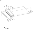
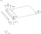
- FIG. 1 is a perspective view of a backlight unit according to an exemplary embodiment of the invention.
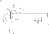
- FIG. 2 is a cross-sectional view taken along line I-I' of FIG. 1 .
- FIG. 3 is an arrangement view seen in one direction of FIG. 2 .
- FIG. 4 is an enlarged view of a part of the backlight unit according to the exemplary embodiment of FIG. 1 .
- a backlight unit includes a light guide plate LG, a housing HO which is disposed at one side of the light guide plate LG and accommodates a wavelength converting member Q, and a flexible glass film GR which covers the housing HO.
- the light guide plate LG may guide received light and provide the light to a display panel (not illustrated), which will be described below.
- the light guide plate LG may include an upper surface US and a lower surface LS opposing each other and a side surface SS connecting the upper surface US and the lower surface LS.
- Light provided from a light source LS may be projected via the upper surface US of the light guide plate LG. That is, the light guide plate LG may guide light provided from the light source LS to be projected toward the upper surface US or via the upper surface. That is, the upper surface US may be a light output surface.
- FIG. 1 illustrates a case in which the upper surface US includes a flat surface
- the shape of the upper surface US is not limited thereto. That is, in another exemplary embodiment, a functional pattern that performs an optical function may be provided on the upper surface US.
- the functional pattern may include a plurality of protruding patterns or recessed patterns.
- the lower surface LS may be disposed to be opposite to the upper surface US.
- the lower surface LS may have substantially the same shape as the upper surface US and may be disposed in parallel with the upper surface US.
- the lower surface LS may reflect or scatter light provided from the light source LS and serve to guide light to travel toward the upper surface US.
- FIG. 1 illustrates a case in which the lower surface LS has a flat surface
- the shape of the lower surface LS is not limited thereto. That is, according to another exemplary embodiment, a plurality of functional patterns may be provided on the lower surface LS.
- the functional pattern may be a pattern that performs a reflecting function and/or a scattering function as described above, and the shape and number of the functional patterns are not limited.
- the side surface SS may be disposed between the upper surface US and the lower surface LS. According to an exemplary embodiment, the side surface SS may connect the upper surface US and the lower surface LS.
- the light guide plate LG may include one or more side surfaces SS.
- the light guide plate LG may include four side surfaces SS.
- four side surfaces SS may be presented, for example.
- the side surfaces SS may include two short side surfaces opposing each other and two long side surfaces opposing each other.
- the light source LS which will be described below, may be disposed adjacent to a short side surface of the light guide plate LG. That is, according to an exemplary embodiment, the short side surface of the light guide plate LG adjacent to the light source may be a light incident surface, and the other short side surface opposing the light incident surface may be a light facing surface.
- FIG. 1 illustrates a case in which the short side surfaces extend in a y-axis direction and the long side surfaces extend in an x-axis direction.
- FIG. 1 illustrates a case in which the side surfaces SS include flat surfaces
- the invention is not limited thereto.
- the side surfaces SS may at least partially include one or more inclined surfaces.
- the light guide plate LG may be a glass light guide plate including a glass, for example.
- the housing HO which accommodates the wavelength converting member Q may be disposed at one side of the light guide plate LG.
- Light provided from the light source LS may pass through the wavelength converting member Q and be provided to the light guide plate LG.
- light that has passed through the wavelength converting member Q may be converted into white light, for example, and provided to the light guide plate LG. That is, the wavelength converting member Q may serve to shift a wavelength of provided light.
- the wavelength converting member Q may include a quantum dot.
- the quantum dot included in the wavelength converting member Q may include any one nanocrystal of a Si-based nanocrystal, a II-VI family compound semiconductor nanocrystal, a III-V family compound semiconductor nanocrystal, a IV-VI family compound semiconductor nanocrystal, and a combination thereof.
- the II-VI family compound semiconductor nanocrystal may include at least one of CdS, CdSe, CdTe, ZnS, ZnSe, ZnTe, HgS, HgSe, HgTe, CdSeS, CdSeTe, CdSTe, ZnSeS, ZnSeTe, ZnSTe, HgSeS, HgSeTe, HgSTe, CdZnS, CdZnSe, CdZnTe, CdHgS, CdHgSe, CdHgTe, HgZnS, HgZnSe, HggZnTe, CdZnSeS, CdZnSeTe, CdZnSTe, CdHgSeS, CdHgSeTe, CdHgSTe, HgZnSeS, HgZnSeTe and HgZnSTe, for example.
- the III-V family compound semiconductor nanocrystal may include at least one of GaPAs, AlNP, AlNAs, AlPAs, InNP, InNAs, InPAs, GaAlNP, GaAlNAs, GaAlPAs, GaInNP, GaInNAs, GaInPAs, InAlNP, InAlNAs, and InAlPAs, for example.
- the IV-VI family compound semiconductor nanocrystal may be SbTe, for example.
- the wavelength converting member Q may have a bar shape and extend in a longitudinal direction.
- FIG. 1 illustrates a case in which the wavelength converting member Q extends in the y-axis direction.
- the wavelength converting member Q may extend along the side surface SS of the light guide plate LG.
- the wavelength converting member Q may be disposed to face the light output surface, i.e., the side surface SS adjacent to the light source LS, of the short side surfaces of the light guide plate LG.
- the wavelength converting member Q may continuously extend in one direction. However, the invention is not limited thereto, and according to another exemplary embodiment, the wavelength converting member Q may intermittently extend. That is, although FIG. 1 illustrates a case in which a single wavelength converting member Q is unitary, the invention is not limited thereto. According to another exemplary embodiment, a plurality of wavelength converting members Q may be provided independently of each other.
- the wavelength converting member Q may be accommodated in the housing HO.
- a storage space SP may be defined in the housing HO and the housing HO may have a bar shape extending in the longitudinal direction.
- the longitudinal direction may be the y-axis direction of FIG. 1 .
- a predetermined space may be defined in the housing HO.
- the predetermined space will be referred to as the storage space SP.
- the storage space SP may have one side open and the other side closed.
- the storage space SP may be filled with the wavelength converting member Q.
- the wavelength converting member Q may be sealed by the housing HO and the flexible glass film GR, which will be described below.
- the storage space SP of the housing HO may be sealed by the flexible glass film GR, and accordingly, the wavelength converting member Q disposed in the storage space SP may be shielded from the outside and not exposed to moisture or air.
- the housing HO may be provided by including a glass, for example.
- the housing HO may have the shape of a hollow glass tube, for example.
- the housing HO may include the same type of glass as that of the light guide plate LG.
- the housing HO may include a different type of glass from that of the light guide plate LG.
- the flexible glass film GR which covers the housing HO may be disposed at one side of the housing HO.
- the flexible glass film GR may include glass and have flexibility due to its thickness. According to an exemplary embodiment, the flexible glass film GR may have a thickness in the range of about 5 micrometers ( ⁇ m) to about 50 ⁇ m along a z-direction in FIG. 1 , for example.
- the flexible glass film GR may cover one side of the housing HO, and accordingly, the storage space SP of the housing HO may be sealed. That is, the flexible glass film GR may directly contact the housing HO and the wavelength converting member Q and close an open portion of the storage space SP.
- the housing HO may be disposed between the flexible glass film GR and the light guide plate LG.
- the open portion of the storage space SP of the housing HO may face an outer side of the light guide plate LG and be covered with the flexible glass film GR.
- the closed portion of the housing HO may contact a side surface of the light guide plate LG.
- the closed portion of the housing HO may contact the light guide plate LG but may not be welded thereto.
- the flexible glass film GR may include a cover portion 101, a spaced-apart portion 102, and a contact portion 103.
- the cover portion 101 of the flexible glass film GR may cover the storage space SP of the housing HO and seal the storage space SP.
- the cover portion 101 may be welded to the housing HO.
- the cover portion 101 may be welded to the housing HO using a laser welding method, for example, and accordingly, a first laser welding part LB1 may be disposed at a contact surface between the cover portion 101 and the housing HO.
- the first laser welding part LB1 will be described in detail with reference to FIG. 3 .
- the first laser welding part LB1 may include a continuous welding line BL.
- the welding line BL may be continuously provided, and a cross-sectional shape thereof may be a closed shape.
- the welding line BL may have a quadrilateral shape disposed along an outer periphery of the cross-section of the storage space SP (refer to FIG. 3 ).
- the function of the wavelength converting member Q may be considerably deteriorated when the wavelength converting member Q is exposed to moisture and oxygen.
- the storage space SP of the housing HO may be completely sealed, and the wavelength converting member Q may be prevented from being exposed to external moisture and oxygen.
- FIG. 4 is an enlarged view of a part of the contact surface between the cover portion 101 of the flexible glass film GR and the housing HO.
- the first laser welding part LB1 may include a central region A1 and a periphery region A2 disposed outside the central region A1.
- the laser welding part may be provided using a femtosecond laser.
- the femtosecond laser may refer to a laser having a wavelength of femtoseconds.
- the central region A1 of the first laser welding part LB1 may be provided across the contact surface.
- a cross-section of the central region A1 may have an elliptical shape in which a long axis is longer than a short axis.
- the central region A1 has an elliptical cross-section
- the cross-sectional shape of the central region is not limited thereto.
- the central region A1 may have a circular cross-section.
- the following description of the long axis may be replaced with description of a diameter of the circular shape.
- FIG. 4 illustrates a case in which the long axis of the central region A1 is perpendicular to the contact surface
- a direction of the long axis is not limited thereto. That is, the direction of the long-axis may vary depending on a laser irradiation direction.
- a boundary between the housing HO and the cover portion 101 may disappear in the central region A1. That is, the contact surface between the housing HO and the cover portion 101 may not be clearly identified.
- the housing HO may include a first glass material
- the flexible glass film GR may include a second glass material that is different from the first glass material
- the first glass material and the second glass material may have physical properties shown in Table 1 below.
- Table 1 Physical properties First glass material
- Second glass material Candidate 1 Candidate 2
- Young's modulus (Gpa) 68 83 77 73
- the housing HO may include Candidate 1 of the first glass material
- the flexible glass film GR may include Candidate 1 of the second glass material.
- the housing HO may include Candidate 2 of the first glass material
- the flexible glass film GR may include Candidate 2 of the second glass material.
- the central region A may be a region in which the first glass material and the second glass material are mixed without boundary.
- the housing HO and the flexible glass film GR may include the same type of glass.
- the central region A1 may be a region in which the housing HO and the flexible glass film GR are mixed without boundary.
- a width d1 of the long axis of the central region A1 may be in the range of about 10 ⁇ m to about 20 ⁇ m, for example.
- the periphery region A2 may be disposed outside the central region A1 to surround the central region A1.
- the central region A1 may have a circular cross-section.
- a width d2 of the periphery region A2 may be in the range of about 70 ⁇ m to about 100 ⁇ m, for example.
- thermal damage may be applied to the wavelength converting member Q.
- a maximum width of a welding dot BD is in the range of about 70 ⁇ m to about 100 ⁇ m as described above, for example, thermal damage applied to the wavelength converting member Q may be prevented or minimized.
- a laser having a wavelength of femtoseconds may be used to minimize the size of the first laser welding part LB1.
- the housing HO and the flexible glass film GR are welded to each other, and the maximum width of the first laser welding LB1 may be maintained to be about 100 ⁇ m or smaller, for example. Accordingly, damage to the wavelength converting member Q due to heat may be minimized.
- the spaced-apart portion 102 may extend from the cover portion 101 toward an inside of the light guide plate LG. That is, the spaced-apart portion 102 may overlap the upper surface US and/or the lower surface LS of the light guide plate LG.
- the flexible glass film GR has flexibility, the flexible glass film GR may be broken when curved by a predetermined angle or more because the flexible glass film GR basically includes a fragile material. Accordingly, the spaced-apart portion 102 may be gently curved with a predetermined curvature.
- the spaced-apart portion 102 may be provided to be spaced apart from the upper surface US of the light guide plate LG by a predetermined distance.
- the contact portion 103 may extend from the spaced-apart portion 102 toward the inside of the light guide plate LG.
- the contact portion 103 may directly contact the upper surface US of the light guide plate LG.
- the contact portion 103 may be welded to the upper surface US of the light guide plate LG using a laser welding method. Accordingly, a second laser welding part LB2 may be disposed at a contact surface between the contact portion 103 and the upper surface of the light guide plate LG.
- the second laser welding part LB2 may include a plurality of welding dots BD.
- Cross-sections of the welding dots BD may be substantially the same as that described with reference to FIG. 4 . That is, as described with reference to FIG. 4 , each of the welding dots BD may be provided using a femtosecond laser, and accordingly, each of the welding dots BD may include the central region A1 and the periphery region A2.
- the plurality of welding dots BD may be disposed on the same axis.
- FIG. 1 illustrates a case in which the plurality of welding dots BD extends in the y-axis direction, for example.
- FIG. 1 illustrates a case in which the second laser welding part LB2 intermittently extends
- the invention is not limited thereto.
- the second laser welding part LB2 may include the continuous welding line BL.
- the backlight unit may further include the light source LS disposed at one side of the housing HO.
- the light source LS may provide light to the light guide plate LG.
- the light source LS may be disposed adjacent to the side surface of the light guide plate LG.
- the wavelength converting member Q may be disposed between the light source LS and the light guide plate LG.
- the light source LS may include a printed circuit board (“PCB”) 55 and a light emitting diode (“LED”) 56.
- the PCB 55 may support the LED 56.
- the PCB 55 may extend in the longitudinal direction.
- the PCB 55 may extend in the same direction as the wavelength converting member Q, i.e., the y-axis direction in FIG. 2 . That is, the PCB 55 and the wavelength converting member Q may extend in parallel to each other.
- the PCB 55 may include various circuits (not illustrated) which control the LED 56.
- the LED 56 may be disposed on the PCB 55.
- the LED 56 may be an LED which emits blue light or an LED which emits ultraviolet ("UV”) light, for example.
- UV ultraviolet
- a plurality of LEDs 56 may be disposed along the PCB 55. As described above, light emitted from the LEDs 56 may be provided across one of the side surfaces SS, i.e., the light incident surface, of the light guide plate LG via the wavelength converting member Q.
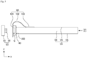
- FIG. 5 is a cross-sectional view of a backlight unit according to another exemplary embodiment of the invention.
- FIG. 6 is a side view of the backlight unit according to the exemplary embodiment of FIG. 5 .
- one surface of the housing HO may be welded to the light guide plate LG.
- a third laser welding part LB3 may be disposed between the housing HO and the light guide plate LG.
- the third laser welding part LB3 may be provided at a contact surface between the side surface SS of the light guide plate LG and the housing HO.
- the third laser welding part LB3 may include the plurality of welding dots BD (refer to FIG. 6 ).
- the cross-sections of the welding dots BD may be substantially the same as that described with reference to FIG. 4 . That is, as described with reference to FIG. 4 , each of the welding dots BD may be provided using a femtosecond laser, and accordingly, each of the welding dots BD may include the central region A1 and the periphery region A2.
- the welding dots BD may be disposed to surround an outer periphery of the wavelength converting member Q. That is, the welding dots BD and the wavelength converting member Q may not overlap each other in the x-axis direction.
- the welding dots BD may cause optical loss due to their physical structures, and when the welding dots BD and the wavelength converting member Q do not overlap each other in the x-axis direction as described above, light that has passed through the wavelength converting member Q may be immediately provided to the light guide plate LG without contacting the welding dots BD.
- FIG. 6 illustrates a case in which the plurality of welding dots BD form a quadrilateral shape
- the shape provided by the welding dots BD is not limited thereto.
- the welding dots BD may be disposed along any one or more line segments selected from four sides of a rectangle.
- FIG. 6 illustrates a case in which the third laser welding part LB3 intermittently extend
- the invention is not limited thereto.
- the third laser welding part LB3 may include the continuous welding line BL (refer to FIG. 3 ).
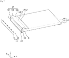
- FIG. 7 is a perspective view of a backlight unit according to another exemplary embodiment of the invention.
- a second laser welding part first line LB2_1 and a second laser welding part second line LB2 2 may be disposed at the contact portion 103 of the flexible glass film GR and the upper surface US of the light guide plate LG.
- the second laser welding part LB2 may include a plurality of lines.
- the second laser welding part first line LB2_1 and the second laser welding part second line LB2_2 may extend in parallel to each other in the y-axis direction.
- the second laser welding part first line LB2_1 and the second laser welding part second line LB2_2 may include the plurality of welding dots BD (refer to FIGS. 1 and 6 ). That is, the plurality of welding dots BD may be disposed along the second laser welding part first line LB2_1 and the second laser welding part second line LB2_2.
- each of the second laser welding part first line LB2_1 and the second laser welding part second line LB2_2 may include the continuous welding line BL.
- the welding dots BD and the welding line BL may be substantially the same as those described above with reference to the backlight unit according to some exemplary embodiments of the invention.
- the second laser welding part LB2 includes the plurality of lines, a welding force between the flexible glass film GR and the light guide plate LG may be strengthened, and accordingly, the flexible glass film GR and the light guide plate LG may be stably fixed to each other.
- FIG. 8 is a perspective view of a backlight unit according to another exemplary embodiment of the invention.
- a second laser welding part LB2_3 may have a closed shape.
- a cross-sectional shape of the second laser welding part LB2_3 may be a closed shape.
- the second laser welding part LB2_3 may draw a closed curve along an outer periphery of the contact surface between the contact portion 103 of the flexible glass film GR and the upper surface US of the light guide plate LG.
- FIG. 8 illustrates a case in which the cross-sectional shape of the second laser welding part LB2_3 is a quadrilateral shape.
- the second laser welding part LB2_3 may include the intermittent welding dots BD (refer to FIGS. 1 and 6 ) or the continuous welding line BL (refer to FIG. 3 ).
- the second laser welding part LB2_3 may minimize optical interference due to the laser welding part while increasing the welding strength between the flexible glass film GR and the light guide plate LG. That is, an overlap between the laser welding part and an optical path of light passing through the light guide plate may be minimized.
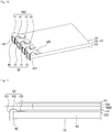
- FIG. 9 is a perspective view of a part of a backlight unit according to another exemplary embodiment of the invention.
- FIG. 10 is a perspective view of the backlight unit to which the exemplary embodiment of FIG. 9 is applied.
- a flexible glass film GR0 may include a plurality of sub-flexible glass films 21, 22, 23, and 24.
- the flexible glass film GR0 may include a first sub-flexible glass film 21, a second sub-flexible glass film 22, a third sub-flexible glass film 23, and a fourth sub-flexible glass film 24.
- FIG. 9 illustrates a case in which the flexible glass film GR0 includes the four sub-flexible glass films, this is merely illustrative, and the number of sub-flexible glass films is not limited thereto. According to another exemplary embodiment, the number of sub-flexible glass films may be less than or greater than four.
- a wavelength converting member Q2 may include a plurality of sub-wavelength converting members 11, 12, 13, and 14 to correspond to the plurality of sub-flexible glass films.
- the wavelength converting member Q2 may include a first sub-wavelength converting member 11, a second sub-wavelength converting member 12, a third sub-wavelength converting member 13, and a fourth sub-wavelength converting member 14.
- a housing HO1 may include four storage spaces SP1, SP2, SP3, and SP4 separated from each other.
- the four storage spaces SP1, SP2, SP3, and SP4 will be referred to as a first storage space SP1, a second storage space SP2, a third storage space SP3, and a fourth storage space SP4.
- the first storage space SP1, the second storage space SP2, the third storage space SP3, and the fourth storage space SP4 may be filled with the first sub-wavelength converting member 11, the second sub-wavelength converting member 12, the third sub-wavelength converting member 13, and the fourth sub-wavelength converting member 14, respectively.
- first sub-flexible glass film 21, the second sub-flexible glass film 22, the third sub-flexible glass film 23, and the fourth sub-flexible glass film 24 may cover the first storage space SP1, the second storage space SP2, the third storage space SP3, and the fourth storage space SP4, respectively. Accordingly, the first sub-wavelength converting member 11, the second sub-wavelength converting member 12, the third sub-wavelength converting member 13, and the fourth sub-wavelength converting member 14 may be sealed.
- Each of the first sub-flexible glass film 21, the second sub-flexible glass film 22, the third sub-flexible glass film 23, and the fourth sub-flexible glass film 24 may include a cover portion, a spaced-apart portion, and a contact portion.
- the cover portion, the spaced-apart portion, and the contact portion of each of the first sub-flexible glass film 21, the second sub-flexible glass film 22, and the third sub-flexible glass film 23 may be substantially the same as those described above with reference to the flexible glass film GR according to the exemplary embodiment of FIG. 1 .
- the first laser welding part LB1 may be generated between the housing HO1 and each of the first sub-flexible glass film 21, the second sub-flexible glass film 22, and the third sub-flexible glass film 23.
- the first laser welding part LB1 may include the continuous welding line BL (refer to FIG. 3 ), and the welding line BL may be provided along outer peripheries of the first storage space SP1, the second storage space SP2, the third storage space SP3, and the fourth storage space SP4.
- Each of the first sub-flexible glass film 21, the second sub-flexible glass film 22, and the third sub-flexible glass film 23 may include the spaced-apart portion overlapping the light guide plate LG while being spaced a predetermined distance apart therefrom.
- each of the first sub-flexible glass film 21, the second sub-flexible glass film 22, the third sub-flexible glass film 23, and the fourth sub-flexible glass film 24 may include the contact portion contacting the light guide plate LG.
- the second laser welding part LB2 may be disposed between the upper surface US of the light guide plate LG and each of the first sub-flexible glass film 21, the second sub-flexible glass film 22, the third sub-flexible glass film 23, and the fourth sub-flexible glass film 24.
- the second laser welding part LB2 may include the intermittent welding dots BD (refer to FIGS. 1 and 6 ) or the continuous welding line BL (refer to FIG. 3 ).
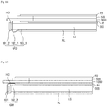
- FIG. 11 is a cross-sectional view of a display device according to an exemplary embodiment of the invention.
- the display device according to an exemplary embodiment of the invention includes a backlight unit and a display panel disposed on the backlight unit.
- the backlight unit may be substantially equal to the backlight unit according to some exemplary embodiments of the invention described above. Consequently, detailed description thereof will be omitted.
- the display panel may include a first substrate 1000, a second substrate 500 facing the first substrate 1000, and a liquid crystal layer (not illustrated) disposed between the first substrate 1000 and the second substrate.
- the first substrate 1000 may be an array substrate on which a plurality of transistors is disposed
- the second substrate 500 may be a color filter substrate on which a color filter is disposed.
- a color filter may be disposed on the first substrate 1000. That is, the display panel may be a display panel having a color filter -on-array ("COA") structure, for example.
- COA color filter -on-array
- the first substrate 1000 and/or the second substrate 500 may include glass.
- the first substrate 1000 may overlap the second substrate 500.
- a driver (not illustrated), a PCB (not illustrated), and the like may be disposed at a region on the first substrate 1000 not overlapping the second substrate 500.
- the first substrate 1000 may have a wider area than the second substrate 500.
- the invention is not limited thereto, and according to another exemplary embodiment, the second substrate 500 may have a wider area than the first substrate 1000.
- the display device may further include a first polarizing plate P1, a second polarizing plate P2, an optical sheet 300, and a reflective layer RL.
- the first polarizing plate P1 and the second polarizing plate P2 may be disposed at an outside of the display panel.
- Only light vibrating in a specific direction of provided light may pass through the first polarizing plate P1 and the second polarizing plate P2, and remaining light may be shielded or reflected by the first polarizing plate P1 and the second polarizing plate P2.
- polarizing directions of the first polarizing plate P1 and the second polarizing plate P2 may be different from each other.
- the first polarizing plate P1 and the second polarizing plate P2 may be disposed inside the display panel.
- the first polarizing plate P1 and the second polarizing plate P2 may be in-cell polarizing plates.
- the first polarizing plate P1 and/or the second polarizing plate P2 may include a wire-grid polarizer ("WGP"), for example.
- WGP wire-grid polarizer
- the reflective layer RL may be disposed below the light guide plate LG.
- the reflective layer RL may serve to reflect light that has passed through the lower surface LS of the light guide plate LG toward the upper surface US again.
- the reflective layer RL may perform specular reflection and/or diffuse reflection.
- the reflective layer RL may be provided in a sheet shape. Also, a plurality of functional patterns may be provided on the reflective layer RL.
- the optical sheet 300 may be disposed above the light guide plate LG. According to an exemplary embodiment, a single optical sheet 300 may be present, and the optical sheet 300 may perform complex functions such as scattering and diffusing.
- a plurality of optical sheets 300 may be present, and the optical sheets 300 may perform functions independent of each other.
- FIG. 12 is a cross-sectional view of a display device according to another exemplary embodiment of the invention.
- a cover portion 101_1 of a flexible glass film GR1 may be disposed between the housing HO and the light guide plate LG.
- cover portion 101_1 and the housing HO are welded using a laser is that same as in the backlight unit according to some exemplary embodiments of the invention described above. However, unlike the exemplary embodiments described above, the cover portion 101_1 may directly contact the light guide plate LG in this exemplary embodiment.
- the cover portion 101_1 and the light guide plate LG may contact each other but not be welded to each other.
- the cover portion 101_1 and the light guide plate LG may be welded to each other using a laser.
- the third laser welding part may be disposed between the cover portion 101_1 and the light guide plate LG.
- FIG. 13 is a cross-sectional view of a display device according to another exemplary embodiment of the invention.
- a flexible glass film GR2 may contact the lower surface LS of the light guide plate LG.
- the flexible glass film GR2 may extend toward the lower surface LS of the light guide plate LG, and accordingly, a spaced-apart portion 102_1 may face the lower surface LS of the light guide plate LG, and a contact portion 103_1 may contact the lower surface LS of the light guide plate LG.
- the contact portion 103_1 and the lower surface LS of the light guide plate LG may be welded using a laser. Accordingly, the fourth laser welding part LB4 may be disposed between the contact portion 103_1 and the lower surface LS.
- FIG. 14 is a cross-sectional view of a display device according to another exemplary embodiment of the invention.
- the display device is different from the exemplary embodiment of FIG. 1 in that a cover portion 101_2 of a flexible glass film GR3 is disposed between the housing HO and the light guide plate LG and the contact portion 103_1 contacts the lower surface of the light guide plate LG.
- cover portion 101_2 is disposed between the housing HO and the light guide plate LG may be substantially the same as that described above with reference to FIG. 12 .
- the fact that the contact portion 103_1 contacts the lower surface LS of the light guide plate LG may be substantially the same as that described above with reference to FIG. 13 . Consequently, detailed description thereof will be omitted.
- FIG. 15 is a cross-sectional view of a display device according to another exemplary embodiment of the invention.
- a flexible glass film GR4 may include the cover portion 101 and a panel contact portion 102_2.
- the cover portion 101 may be substantially the same as that described above according to some exemplary embodiments of the invention. Consequently, detailed description thereof will be omitted.
- the panel contact portion 102_2 may contact a lower surface of the first substrate 1000.
- the panel contact portion 102_2 may contact the lower surface of the first substrate 1000 but not be welded thereto.
- the panel contact portion 102_2 may be welded to the first substrate 1000.
- the first substrate 1000 may include glass.
- the first substrate 1000 and the panel contact portion 102_2 may be welded using a laser. That is, a fourth laser welding part (not illustrated) may be disposed between the first substrate 1000 and the panel contact portion 102_2.
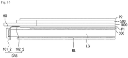
- FIG. 16 is a cross-sectional view of a display device according to another exemplary embodiment of the invention.
- a flexible glass film GR5 includes the cover portion 101_2 and the panel contact portion 102_2, and the cover portion 101_2 may be disposed between the light guide plate LG and the housing HO.
- cover portion 101_2 is disposed between the light guide plate LG and the housing HO may be substantially the same as that described above with reference to FIG. 14 . Consequently, detailed description thereof will be omitted.
- the wavelength converting member Q may be reliably fixed while deterioration of optical characteristics in the display device is minimized.
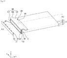
- FIG. 17 is a perspective view of a backlight unit according to an exemplary embodiment of the invention.
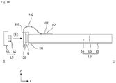
- FIG. 18 is a cross-sectional view taken along line II-II' of FIG. 17
- the backlight unit may further include a cover glass 150 which seals the housing HO.
- the cover glass 150 may be disposed at one side of the housing HO. According to an exemplary embodiment, the cover glass 150 may be disposed between the flexible glass film GR and the housing HO. In other words, one side of the cover glass 150 may contact the flexible glass film GR, and the other side thereof may contact the housing HO.
- the cover glass 150 may include a glass material.
- the cover glass 150 may seal an inner space of the housing HO. That is, by closing an open portion of the housing HO, the cover glass 150 may seal the wavelength converting member Q disposed in the inner space of the housing HO.
- the cover glass 150 and the housing HO may be welded using a laser. That is, a fifth laser welding part may be disposed between the cover glass 150 and the housing HO.
- the fifth laser welding part may have a shape and structure that are substantially the same as those of the first laser welding part LB1 described above with reference to FIGS. 1 to 3 .
- the cover glass 150 and the flexible glass film GR may be welded using a laser. That is, a sixth laser welding part may be disposed between the cover glass 150 and the flexible glass film GR.
- the sixth laser welding part may include the welding dots BD (refer to FIGS. 1 and 6 ) and/or the welding line BL (refer to FIG. 3 ).
- FIGS. 17 and 18 illustrate a configuration in which the cover glass 150 and the housing HO are disposed independent of each other, the invention is not limited thereto.
- the cover glass 150 and the housing HO may be unitary.
- the housing HO may include the cover glass 150, and accordingly, the housing HO itself may seal the wavelength converting member Q.
- LCD liquid crystal display
- the method of manufacturing a display device includes preparing the light guide plate LG and the housing HO which is disposed at one side of the light guide plate LG and accommodates the wavelength converting member Q, and placing the flexible glass film GR at one side of the housing HO and welding the housing HO and the flexible glass film GR using a femtosecond laser.
- the light guide plate LG and the wavelength converting member Q may be the same as those described above with reference to some exemplary embodiments of the invention.
- the placing of the flexible glass film GR at the side of the housing HO and the welding of the housing HO and the flexible glass film GR using the femtosecond laser may include irradiating the contact surface between the flexible glass film GR and the housing HO with the femtosecond laser, for example.
- the first laser welding part LB1 may be disposed between the flexible glass film GR and the housing HO (refer to FIG. 1 ). Also, as described above, the first laser welding part LB1 may include the welding line BL.
- the welding line BL may be provided using a method of continuously irradiating the femtosecond laser. That is, when the laser is continuously irradiated while moving a focus of the femtosecond laser, the continuous welding line BL may be provided.
- cross-section of the welding line BL may include the central region A1 and the periphery region A2 is the same as that described above with reference to FIG. 4 .
- the method of manufacturing a display device may further include welding the flexible glass film GR and the light guide plate LG using a femtosecond laser.
- the flexible glass film GR may include the cover portion 101, the spaced-apart portion 102, and the contact portion 103.
- the contact portion 103 may contact the upper surface US or the lower surface LS of the light guide plate LG.
- a portion between the flexible glass film GR and the light guide plate LG may be irradiated with the femtosecond laser.
- the second laser welding part LB2 may be disposed between the flexible glass film GR and the light guide plate LG.
- the second laser welding part LB2 may include the welding dots BD and/or the welding line BL.
- the welding dots BD may be provided using a method of intermittently irradiating the femtosecond laser. That is, when the laser is intermittently irradiated while moving the focus of the femtosecond laser, the plurality of welding dots BD may be provided.
- the welding line BL may be provided using a method of continuously irradiating the femtosecond laser. That is, when the laser is continuously irradiated while moving the focus of the femtosecond laser, the continuous welding line BL may be provided.
- cross-section of the welding line BL may include the central region A1 and the periphery region A2 is the same as that described above with reference to FIG. 4 .
- the method of manufacturing a display device may further include welding the housing HO and the light guide plate LG by irradiating a portion therebetween with the femtosecond laser, for example.
- the third laser welding part LB3 may be disposed between the housing HO and the light guide plate LG.
- the third laser welding part LB3 may include the welding line BL and/or the welding dots BD is the same as that described above according to some exemplary embodiments of the invention.
- a housing which accommodates the light guide plate and the wavelength converting member can be reliably fixed.
Landscapes
- Physics & Mathematics (AREA)
- Nonlinear Science (AREA)
- General Physics & Mathematics (AREA)
- Optics & Photonics (AREA)
- Mathematical Physics (AREA)
- Chemical & Material Sciences (AREA)
- Crystallography & Structural Chemistry (AREA)
- Engineering & Computer Science (AREA)
- Manufacturing & Machinery (AREA)
- Planar Illumination Modules (AREA)
- Devices For Indicating Variable Information By Combining Individual Elements (AREA)
- Liquid Crystal (AREA)
Claims (16)
- Unité de rétro-éclairage comprenant :une plaque de guidage de lumière (LG) ;un boîtier (40) qui est disposé au niveau d'un côté de la plaque de guidage de lumière (LG) et loge un organe de conversion de longueur d'onde (Q) ; etun film en verre flexible (GR) qui couvre un côté du boîtier (40),dans laquelle une première partie de soudage laser (LB1) est disposée entre le film en verre flexible (GR) et le boîtier (40).
- Unité de rétro-éclairage selon la revendication 1, dans laquelle le film en verre flexible (GR) comporte :une portion de couverture (101) qui couvre le côté du boîtier (40) ;une portion espacée (102) chevauchant la plaque de guidage de lumière (LG) et espacée de la plaque de guidage de lumière (LG) ; etune portion de contact (103) en contact avec la plaque de guidage de lumière (LG).
- Unité de rétro-éclairage selon la revendication 2, dans laquelle la portion espacée (102) est courbée avec une courbure prédéterminée.
- Unité de rétro-éclairage selon la revendication 2, dans laquelle une seconde partie de soudage laser (LB2) est disposée entre la plaque de guidage de lumière (LG) et la portion de contact (103).
- Unité de rétro-éclairage selon la revendication 4, dans laquelle la seconde partie de soudage laser (LB2) comporte une pluralité de points de soudage (BD).
- Unité de rétro-éclairage selon la revendication 4, dans laquelle la seconde partie de soudage laser (LB2) comporte une première ligne et une seconde ligne qui s'étendent parallèlement l'une à l'autre et comportent une pluralité de points de soudage (BD) ou une ligne de soudage (BL).
- Unité de rétro-éclairage selon la revendication 1, dans laquelle une épaisseur du film en verre flexible (GR) est dans une plage d'environ 5 micromètres à environ 50 micromètres.
- Unité de rétro-éclairage selon la revendication 1, dans laquelle la première partie de soudage laser (LB1) comporte une ligne de soudage continue.
- Unité de rétro-éclairage selon la revendication 1, dans laquelle une seconde partie de soudage laser (LB2) est disposée entre la plaque de guidage de lumière (LG) et le boîtier (40).
- Unité de rétro-éclairage selon la revendication 1, dans laquelle l'organe de conversion de longueur d'onde (Q) comporte une pluralité de sous-organes de conversion de longueur d'onde (11, 12, 13, 14), et le film en verre flexible (GR) comporte une pluralité de sous-films en verre flexible (21, 22, 23, 24) correspondant à la pluralité de sous-organes de conversion de longueur d'onde (11, 12, 13, 14).
- Dispositif d'affichage comprenant :une unité de rétro-éclairage selon au moins l'une des revendications 1 à 10 ;un panneau d'affichage disposé au-dessus de l'unité de rétro-éclairage.
- Dispositif d'affichage selon la revendication 11, dans lequel :le panneau d'affichage comporte un premier substrat et un second substrat face à face ; etle film en verre flexible (GR) comporte une portion de couverture qui couvre le côté du boîtier et une portion de contact de panneau s'étendant depuis la portion de couverture et soudée au premier substrat.
- Procédé de fabrication d'un dispositif d'affichage, le procédé comprenant :la préparation d'une plaque de guidage de lumière (LG) et d'un boîtier (40) qui est disposé au niveau d'un côté de la plaque de guidage de lumière (LG) et loge un organe de conversion de longueur d'onde (Q) ; etle placement d'un film en verre flexible (GR) au niveau d'un côté du boîtier (40) et le soudage du boîtier (40) et du film en verre flexible (GR) à l'aide d'un laser femtoseconde.
- Procédé selon la revendication 13, dans lequel :le film en verre flexible (GR) comporte une portion de couverture soudée au boîtier (40), une portion espacée (102) s'étendant depuis la portion de couverture (101), et une portion de contact (103) s'étendant depuis la portion espacée et en contact avec la plaque de guidage de lumière (LG) ; etle procédé comprend en outre le soudage de la plaque de guidage de lumière (LG) et de la portion de contact (103) à l'aide d'un laser femtoseconde.
- Procédé selon au moins l'une des revendications 13 ou 14, comprenant en outre le soudage de la plaque de guidage de lumière (LG) et du boîtier (40) à l'aide d'un laser femtoseconde.
- Unité de rétro-éclairage selon au moins l'une des revendications 1 à 12, dans laquelle le boîtier comporte en outre un verre de couverture disposé au niveau du côté, et la première partie de soudage laser (LB1) est disposée entre le verre de couverture et le film en verre flexible (GR).
Applications Claiming Priority (1)
| Application Number | Priority Date | Filing Date | Title |
|---|---|---|---|
| KR1020170103675A KR102446538B1 (ko) | 2017-08-16 | 2017-08-16 | 백라이트 유닛, 표시 장치 및 표시 장치의 제조 방법 |
Publications (2)
| Publication Number | Publication Date |
|---|---|
| EP3444660A1 EP3444660A1 (fr) | 2019-02-20 |
| EP3444660B1 true EP3444660B1 (fr) | 2020-04-29 |
Family
ID=63144867
Family Applications (1)
| Application Number | Title | Priority Date | Filing Date |
|---|---|---|---|
| EP18187202.9A Active EP3444660B1 (fr) | 2017-08-16 | 2018-08-03 | Unité de rétroéclairage, dispositif d'affichage et procédé de fabrication d'un dispositif d'affichage |
Country Status (5)
| Country | Link |
|---|---|
| US (1) | US10845647B2 (fr) |
| EP (1) | EP3444660B1 (fr) |
| JP (1) | JP2019036531A (fr) |
| KR (1) | KR102446538B1 (fr) |
| CN (1) | CN109407393B (fr) |
Families Citing this family (2)
| Publication number | Priority date | Publication date | Assignee | Title |
|---|---|---|---|---|
| USD877147S1 (en) * | 2014-07-04 | 2020-03-03 | Sakai Display Products Corporation | Image display |
| CN110213918B (zh) * | 2019-06-24 | 2021-11-23 | Oppo广东移动通信有限公司 | 壳体组件及电子设备 |
Family Cites Families (13)
| Publication number | Priority date | Publication date | Assignee | Title |
|---|---|---|---|---|
| US8159628B2 (en) * | 2009-03-31 | 2012-04-17 | Chimei Innolux Corporation | Method of fastening a circuit assembly to a light guide in a manufacturing process of a LCD-display |
| KR101269007B1 (ko) * | 2009-05-08 | 2013-05-29 | 엘지디스플레이 주식회사 | 액정표시장치 및 이의 제조방법 |
| CN102313195B (zh) * | 2010-07-06 | 2014-06-18 | 乐金显示有限公司 | 用于制造导光板的装置和具有该导光板的背光单元 |
| CN203442699U (zh) * | 2013-09-09 | 2014-02-19 | 深圳Tcl新技术有限公司 | 背光模组 |
| KR102146844B1 (ko) * | 2013-12-23 | 2020-08-24 | 엘지디스플레이 주식회사 | 백라이트 유닛 및 이를 이용한 디스플레이 장치 |
| KR102171590B1 (ko) * | 2014-02-14 | 2020-10-30 | 삼성디스플레이 주식회사 | 백라이트 유닛 |
| US20170279247A1 (en) | 2014-08-25 | 2017-09-28 | Corning Incorporated | Sealed device and methods for making the same |
| KR101686737B1 (ko) * | 2015-04-30 | 2016-12-14 | 엘지전자 주식회사 | 광 변환 플레이트, 이를 포함하는 발광 다이오드 패키지, 백라이트 유닛 및 표시장치 |
| CN107635935A (zh) * | 2015-05-15 | 2018-01-26 | 康宁股份有限公司 | 具有激光切割边缘的玻璃制品及其制造方法 |
| CN106468799A (zh) * | 2015-08-20 | 2017-03-01 | 夏普株式会社 | 导光板、边光型背光源和液晶显示装置 |
| KR102384407B1 (ko) * | 2015-10-01 | 2022-04-08 | 삼성디스플레이 주식회사 | 표시 장치 및 이의 제조 방법 |
| KR101778895B1 (ko) | 2016-11-24 | 2017-09-14 | 엘지전자 주식회사 | 백라이트 유닛 및 이를 포함하는 표시장치 |
| KR102627073B1 (ko) | 2016-11-30 | 2024-01-19 | 삼성디스플레이 주식회사 | 백라이트 유닛, 표시 장치 및 표시 장치의 제조 방법 |
-
2017
- 2017-08-16 KR KR1020170103675A patent/KR102446538B1/ko active Active
-
2018
- 2018-07-17 JP JP2018133968A patent/JP2019036531A/ja active Pending
- 2018-07-23 US US16/042,613 patent/US10845647B2/en active Active
- 2018-08-03 EP EP18187202.9A patent/EP3444660B1/fr active Active
- 2018-08-10 CN CN201810906924.6A patent/CN109407393B/zh active Active
Non-Patent Citations (1)
| Title |
|---|
| None * |
Also Published As
| Publication number | Publication date |
|---|---|
| US20190056623A1 (en) | 2019-02-21 |
| US10845647B2 (en) | 2020-11-24 |
| KR20190019247A (ko) | 2019-02-27 |
| JP2019036531A (ja) | 2019-03-07 |
| EP3444660A1 (fr) | 2019-02-20 |
| CN109407393A (zh) | 2019-03-01 |
| CN109407393B (zh) | 2023-05-05 |
| KR102446538B1 (ko) | 2022-09-26 |
Similar Documents
| Publication | Publication Date | Title |
|---|---|---|
| US11035999B2 (en) | Backlight unit, display device and manufacturing method of display device | |
| US9645305B2 (en) | Backlight unit | |
| KR101657954B1 (ko) | 백라이트 어셈블리 및 이를 포함하는 표시 장치 | |
| US9671546B2 (en) | Backlight assembly and display device having the same | |
| KR102126176B1 (ko) | 파장 변환 부재 및 그 제조 방법, 및 이를 포함하는 백라이트 어셈블리 | |
| KR102171590B1 (ko) | 백라이트 유닛 | |
| US9519161B2 (en) | Wavelength conversion member, backlight assembly, and display device including the same | |
| KR20150092798A (ko) | 양자점바 수납 용기 및 이를 포함하는 백라이트 유닛 | |
| US9971085B2 (en) | Light source module and backlight unit including the same | |
| US9835316B2 (en) | Frame and light source module including the same | |
| KR20150094871A (ko) | 파장 변환 부재 및 그 제조 방법, 및 이를 포함하는 백라이트 어셈블리 | |
| US10845647B2 (en) | Backlight unit, display device, and method of manufacturing display device | |
| KR20160065063A (ko) | 백라이트 어셈블리 및 이를 포함하는 표시 장치 | |
| TWM562403U (zh) | 背光組合 | |
| US10578916B2 (en) | Backlight unit, display device and method for manufacturing display device | |
| TWI708100B (zh) | 光學元件 |
Legal Events
| Date | Code | Title | Description |
|---|---|---|---|
| PUAI | Public reference made under article 153(3) epc to a published international application that has entered the european phase |
Free format text: ORIGINAL CODE: 0009012 |
|
| STAA | Information on the status of an ep patent application or granted ep patent |
Free format text: STATUS: THE APPLICATION HAS BEEN PUBLISHED |
|
| AK | Designated contracting states |
Kind code of ref document: A1 Designated state(s): AL AT BE BG CH CY CZ DE DK EE ES FI FR GB GR HR HU IE IS IT LI LT LU LV MC MK MT NL NO PL PT RO RS SE SI SK SM TR |
|
| AX | Request for extension of the european patent |
Extension state: BA ME |
|
| STAA | Information on the status of an ep patent application or granted ep patent |
Free format text: STATUS: REQUEST FOR EXAMINATION WAS MADE |
|
| 17P | Request for examination filed |
Effective date: 20190815 |
|
| RBV | Designated contracting states (corrected) |
Designated state(s): AL AT BE BG CH CY CZ DE DK EE ES FI FR GB GR HR HU IE IS IT LI LT LU LV MC MK MT NL NO PL PT RO RS SE SI SK SM TR |
|
| RIC1 | Information provided on ipc code assigned before grant |
Ipc: G02F 1/1335 20060101AFI20191127BHEP |
|
| GRAP | Despatch of communication of intention to grant a patent |
Free format text: ORIGINAL CODE: EPIDOSNIGR1 |
|
| STAA | Information on the status of an ep patent application or granted ep patent |
Free format text: STATUS: GRANT OF PATENT IS INTENDED |
|
| INTG | Intention to grant announced |
Effective date: 20200109 |
|
| GRAS | Grant fee paid |
Free format text: ORIGINAL CODE: EPIDOSNIGR3 |
|
| GRAA | (expected) grant |
Free format text: ORIGINAL CODE: 0009210 |
|
| STAA | Information on the status of an ep patent application or granted ep patent |
Free format text: STATUS: THE PATENT HAS BEEN GRANTED |
|
| AK | Designated contracting states |
Kind code of ref document: B1 Designated state(s): AL AT BE BG CH CY CZ DE DK EE ES FI FR GB GR HR HU IE IS IT LI LT LU LV MC MK MT NL NO PL PT RO RS SE SI SK SM TR |
|
| REG | Reference to a national code |
Ref country code: GB Ref legal event code: FG4D |
|
| REG | Reference to a national code |
Ref country code: CH Ref legal event code: EP |
|
| REG | Reference to a national code |
Ref country code: NL Ref legal event code: FP |
|
| REG | Reference to a national code |
Ref country code: AT Ref legal event code: REF Ref document number: 1264199 Country of ref document: AT Kind code of ref document: T Effective date: 20200515 |
|
| REG | Reference to a national code |
Ref country code: DE Ref legal event code: R096 Ref document number: 602018004141 Country of ref document: DE |
|
| REG | Reference to a national code |
Ref country code: IE Ref legal event code: FG4D |
|
| REG | Reference to a national code |
Ref country code: LT Ref legal event code: MG4D |
|
| PG25 | Lapsed in a contracting state [announced via postgrant information from national office to epo] |
Ref country code: NO Free format text: LAPSE BECAUSE OF FAILURE TO SUBMIT A TRANSLATION OF THE DESCRIPTION OR TO PAY THE FEE WITHIN THE PRESCRIBED TIME-LIMIT Effective date: 20200729 Ref country code: FI Free format text: LAPSE BECAUSE OF FAILURE TO SUBMIT A TRANSLATION OF THE DESCRIPTION OR TO PAY THE FEE WITHIN THE PRESCRIBED TIME-LIMIT Effective date: 20200429 Ref country code: PT Free format text: LAPSE BECAUSE OF FAILURE TO SUBMIT A TRANSLATION OF THE DESCRIPTION OR TO PAY THE FEE WITHIN THE PRESCRIBED TIME-LIMIT Effective date: 20200831 Ref country code: IS Free format text: LAPSE BECAUSE OF FAILURE TO SUBMIT A TRANSLATION OF THE DESCRIPTION OR TO PAY THE FEE WITHIN THE PRESCRIBED TIME-LIMIT Effective date: 20200829 Ref country code: SE Free format text: LAPSE BECAUSE OF FAILURE TO SUBMIT A TRANSLATION OF THE DESCRIPTION OR TO PAY THE FEE WITHIN THE PRESCRIBED TIME-LIMIT Effective date: 20200429 Ref country code: LT Free format text: LAPSE BECAUSE OF FAILURE TO SUBMIT A TRANSLATION OF THE DESCRIPTION OR TO PAY THE FEE WITHIN THE PRESCRIBED TIME-LIMIT Effective date: 20200429 Ref country code: GR Free format text: LAPSE BECAUSE OF FAILURE TO SUBMIT A TRANSLATION OF THE DESCRIPTION OR TO PAY THE FEE WITHIN THE PRESCRIBED TIME-LIMIT Effective date: 20200730 |
|
| PGFP | Annual fee paid to national office [announced via postgrant information from national office to epo] |
Ref country code: DE Payment date: 20200806 Year of fee payment: 3 Ref country code: FR Payment date: 20200811 Year of fee payment: 3 |
|
| REG | Reference to a national code |
Ref country code: AT Ref legal event code: MK05 Ref document number: 1264199 Country of ref document: AT Kind code of ref document: T Effective date: 20200429 |
|
| PG25 | Lapsed in a contracting state [announced via postgrant information from national office to epo] |
Ref country code: BG Free format text: LAPSE BECAUSE OF FAILURE TO SUBMIT A TRANSLATION OF THE DESCRIPTION OR TO PAY THE FEE WITHIN THE PRESCRIBED TIME-LIMIT Effective date: 20200729 Ref country code: LV Free format text: LAPSE BECAUSE OF FAILURE TO SUBMIT A TRANSLATION OF THE DESCRIPTION OR TO PAY THE FEE WITHIN THE PRESCRIBED TIME-LIMIT Effective date: 20200429 Ref country code: RS Free format text: LAPSE BECAUSE OF FAILURE TO SUBMIT A TRANSLATION OF THE DESCRIPTION OR TO PAY THE FEE WITHIN THE PRESCRIBED TIME-LIMIT Effective date: 20200429 Ref country code: HR Free format text: LAPSE BECAUSE OF FAILURE TO SUBMIT A TRANSLATION OF THE DESCRIPTION OR TO PAY THE FEE WITHIN THE PRESCRIBED TIME-LIMIT Effective date: 20200429 |
|
| PG25 | Lapsed in a contracting state [announced via postgrant information from national office to epo] |
Ref country code: AL Free format text: LAPSE BECAUSE OF FAILURE TO SUBMIT A TRANSLATION OF THE DESCRIPTION OR TO PAY THE FEE WITHIN THE PRESCRIBED TIME-LIMIT Effective date: 20200429 |
|
| PG25 | Lapsed in a contracting state [announced via postgrant information from national office to epo] |
Ref country code: DK Free format text: LAPSE BECAUSE OF FAILURE TO SUBMIT A TRANSLATION OF THE DESCRIPTION OR TO PAY THE FEE WITHIN THE PRESCRIBED TIME-LIMIT Effective date: 20200429 Ref country code: EE Free format text: LAPSE BECAUSE OF FAILURE TO SUBMIT A TRANSLATION OF THE DESCRIPTION OR TO PAY THE FEE WITHIN THE PRESCRIBED TIME-LIMIT Effective date: 20200429 Ref country code: AT Free format text: LAPSE BECAUSE OF FAILURE TO SUBMIT A TRANSLATION OF THE DESCRIPTION OR TO PAY THE FEE WITHIN THE PRESCRIBED TIME-LIMIT Effective date: 20200429 Ref country code: SM Free format text: LAPSE BECAUSE OF FAILURE TO SUBMIT A TRANSLATION OF THE DESCRIPTION OR TO PAY THE FEE WITHIN THE PRESCRIBED TIME-LIMIT Effective date: 20200429 Ref country code: CZ Free format text: LAPSE BECAUSE OF FAILURE TO SUBMIT A TRANSLATION OF THE DESCRIPTION OR TO PAY THE FEE WITHIN THE PRESCRIBED TIME-LIMIT Effective date: 20200429 Ref country code: IT Free format text: LAPSE BECAUSE OF FAILURE TO SUBMIT A TRANSLATION OF THE DESCRIPTION OR TO PAY THE FEE WITHIN THE PRESCRIBED TIME-LIMIT Effective date: 20200429 Ref country code: ES Free format text: LAPSE BECAUSE OF FAILURE TO SUBMIT A TRANSLATION OF THE DESCRIPTION OR TO PAY THE FEE WITHIN THE PRESCRIBED TIME-LIMIT Effective date: 20200429 Ref country code: RO Free format text: LAPSE BECAUSE OF FAILURE TO SUBMIT A TRANSLATION OF THE DESCRIPTION OR TO PAY THE FEE WITHIN THE PRESCRIBED TIME-LIMIT Effective date: 20200429 |
|
| REG | Reference to a national code |
Ref country code: DE Ref legal event code: R097 Ref document number: 602018004141 Country of ref document: DE |
|
| PG25 | Lapsed in a contracting state [announced via postgrant information from national office to epo] |
Ref country code: PL Free format text: LAPSE BECAUSE OF FAILURE TO SUBMIT A TRANSLATION OF THE DESCRIPTION OR TO PAY THE FEE WITHIN THE PRESCRIBED TIME-LIMIT Effective date: 20200429 Ref country code: SK Free format text: LAPSE BECAUSE OF FAILURE TO SUBMIT A TRANSLATION OF THE DESCRIPTION OR TO PAY THE FEE WITHIN THE PRESCRIBED TIME-LIMIT Effective date: 20200429 |
|
| PLBE | No opposition filed within time limit |
Free format text: ORIGINAL CODE: 0009261 |
|
| STAA | Information on the status of an ep patent application or granted ep patent |
Free format text: STATUS: NO OPPOSITION FILED WITHIN TIME LIMIT |
|
| PG25 | Lapsed in a contracting state [announced via postgrant information from national office to epo] |
Ref country code: MC Free format text: LAPSE BECAUSE OF FAILURE TO SUBMIT A TRANSLATION OF THE DESCRIPTION OR TO PAY THE FEE WITHIN THE PRESCRIBED TIME-LIMIT Effective date: 20200429 |
|
| 26N | No opposition filed |
Effective date: 20210201 |
|
| PG25 | Lapsed in a contracting state [announced via postgrant information from national office to epo] |
Ref country code: LU Free format text: LAPSE BECAUSE OF NON-PAYMENT OF DUE FEES Effective date: 20200803 |
|
| REG | Reference to a national code |
Ref country code: BE Ref legal event code: MM Effective date: 20200831 |
|
| PG25 | Lapsed in a contracting state [announced via postgrant information from national office to epo] |
Ref country code: SI Free format text: LAPSE BECAUSE OF FAILURE TO SUBMIT A TRANSLATION OF THE DESCRIPTION OR TO PAY THE FEE WITHIN THE PRESCRIBED TIME-LIMIT Effective date: 20200429 |
|
| PG25 | Lapsed in a contracting state [announced via postgrant information from national office to epo] |
Ref country code: BE Free format text: LAPSE BECAUSE OF NON-PAYMENT OF DUE FEES Effective date: 20200831 Ref country code: IE Free format text: LAPSE BECAUSE OF NON-PAYMENT OF DUE FEES Effective date: 20200803 |
|
| REG | Reference to a national code |
Ref country code: DE Ref legal event code: R119 Ref document number: 602018004141 Country of ref document: DE |
|
| REG | Reference to a national code |
Ref country code: CH Ref legal event code: PL |
|
| REG | Reference to a national code |
Ref country code: NL Ref legal event code: MM Effective date: 20210901 |
|
| PG25 | Lapsed in a contracting state [announced via postgrant information from national office to epo] |
Ref country code: LI Free format text: LAPSE BECAUSE OF NON-PAYMENT OF DUE FEES Effective date: 20210831 Ref country code: CH Free format text: LAPSE BECAUSE OF NON-PAYMENT OF DUE FEES Effective date: 20210831 |
|
| PG25 | Lapsed in a contracting state [announced via postgrant information from national office to epo] |
Ref country code: TR Free format text: LAPSE BECAUSE OF FAILURE TO SUBMIT A TRANSLATION OF THE DESCRIPTION OR TO PAY THE FEE WITHIN THE PRESCRIBED TIME-LIMIT Effective date: 20200429 Ref country code: MT Free format text: LAPSE BECAUSE OF FAILURE TO SUBMIT A TRANSLATION OF THE DESCRIPTION OR TO PAY THE FEE WITHIN THE PRESCRIBED TIME-LIMIT Effective date: 20200429 Ref country code: CY Free format text: LAPSE BECAUSE OF FAILURE TO SUBMIT A TRANSLATION OF THE DESCRIPTION OR TO PAY THE FEE WITHIN THE PRESCRIBED TIME-LIMIT Effective date: 20200429 |
|
| PG25 | Lapsed in a contracting state [announced via postgrant information from national office to epo] |
Ref country code: NL Free format text: LAPSE BECAUSE OF NON-PAYMENT OF DUE FEES Effective date: 20210901 Ref country code: MK Free format text: LAPSE BECAUSE OF FAILURE TO SUBMIT A TRANSLATION OF THE DESCRIPTION OR TO PAY THE FEE WITHIN THE PRESCRIBED TIME-LIMIT Effective date: 20200429 |
|
| PG25 | Lapsed in a contracting state [announced via postgrant information from national office to epo] |
Ref country code: FR Free format text: LAPSE BECAUSE OF NON-PAYMENT OF DUE FEES Effective date: 20210831 Ref country code: DE Free format text: LAPSE BECAUSE OF NON-PAYMENT OF DUE FEES Effective date: 20220301 |
|
| PGFP | Annual fee paid to national office [announced via postgrant information from national office to epo] |
Ref country code: GB Payment date: 20220720 Year of fee payment: 5 |
|
| GBPC | Gb: european patent ceased through non-payment of renewal fee |
Effective date: 20230803 |
|
| PG25 | Lapsed in a contracting state [announced via postgrant information from national office to epo] |
Ref country code: GB Free format text: LAPSE BECAUSE OF NON-PAYMENT OF DUE FEES Effective date: 20230803 |
|
| PG25 | Lapsed in a contracting state [announced via postgrant information from national office to epo] |
Ref country code: GB Free format text: LAPSE BECAUSE OF NON-PAYMENT OF DUE FEES Effective date: 20230803 |