EP3444662A1 - Modulateur spatial de lumière à cristaux liquides - Google Patents
Modulateur spatial de lumière à cristaux liquides Download PDFInfo
- Publication number
- EP3444662A1 EP3444662A1 EP17186647.8A EP17186647A EP3444662A1 EP 3444662 A1 EP3444662 A1 EP 3444662A1 EP 17186647 A EP17186647 A EP 17186647A EP 3444662 A1 EP3444662 A1 EP 3444662A1
- Authority
- EP
- European Patent Office
- Prior art keywords
- layer
- electron
- liquid crystal
- spatial light
- light modulator
- Prior art date
- Legal status (The legal status is an assumption and is not a legal conclusion. Google has not performed a legal analysis and makes no representation as to the accuracy of the status listed.)
- Withdrawn
Links
Images


Classifications
-
- G—PHYSICS
- G02—OPTICS
- G02F—OPTICAL DEVICES OR ARRANGEMENTS FOR THE CONTROL OF LIGHT BY MODIFICATION OF THE OPTICAL PROPERTIES OF THE MEDIA OF THE ELEMENTS INVOLVED THEREIN; NON-LINEAR OPTICS; FREQUENCY-CHANGING OF LIGHT; OPTICAL LOGIC ELEMENTS; OPTICAL ANALOGUE/DIGITAL CONVERTERS
- G02F1/00—Devices or arrangements for the control of the intensity, colour, phase, polarisation or direction of light arriving from an independent light source, e.g. switching, gating or modulating; Non-linear optics
- G02F1/01—Devices or arrangements for the control of the intensity, colour, phase, polarisation or direction of light arriving from an independent light source, e.g. switching, gating or modulating; Non-linear optics for the control of the intensity, phase, polarisation or colour
- G02F1/13—Devices or arrangements for the control of the intensity, colour, phase, polarisation or direction of light arriving from an independent light source, e.g. switching, gating or modulating; Non-linear optics for the control of the intensity, phase, polarisation or colour based on liquid crystals, e.g. single liquid crystal display cells
- G02F1/133—Constructional arrangements; Operation of liquid crystal cells; Circuit arrangements
- G02F1/135—Liquid crystal cells structurally associated with a photoconducting or a ferro-electric layer, the properties of which can be optically or electrically varied
-
- G—PHYSICS
- G02—OPTICS
- G02F—OPTICAL DEVICES OR ARRANGEMENTS FOR THE CONTROL OF LIGHT BY MODIFICATION OF THE OPTICAL PROPERTIES OF THE MEDIA OF THE ELEMENTS INVOLVED THEREIN; NON-LINEAR OPTICS; FREQUENCY-CHANGING OF LIGHT; OPTICAL LOGIC ELEMENTS; OPTICAL ANALOGUE/DIGITAL CONVERTERS
- G02F1/00—Devices or arrangements for the control of the intensity, colour, phase, polarisation or direction of light arriving from an independent light source, e.g. switching, gating or modulating; Non-linear optics
- G02F1/01—Devices or arrangements for the control of the intensity, colour, phase, polarisation or direction of light arriving from an independent light source, e.g. switching, gating or modulating; Non-linear optics for the control of the intensity, phase, polarisation or colour
- G02F1/13—Devices or arrangements for the control of the intensity, colour, phase, polarisation or direction of light arriving from an independent light source, e.g. switching, gating or modulating; Non-linear optics for the control of the intensity, phase, polarisation or colour based on liquid crystals, e.g. single liquid crystal display cells
- G02F1/133—Constructional arrangements; Operation of liquid crystal cells; Circuit arrangements
- G02F1/135—Liquid crystal cells structurally associated with a photoconducting or a ferro-electric layer, the properties of which can be optically or electrically varied
- G02F1/1354—Liquid crystal cells structurally associated with a photoconducting or a ferro-electric layer, the properties of which can be optically or electrically varied having a particular photoconducting structure or material
-
- G—PHYSICS
- G02—OPTICS
- G02F—OPTICAL DEVICES OR ARRANGEMENTS FOR THE CONTROL OF LIGHT BY MODIFICATION OF THE OPTICAL PROPERTIES OF THE MEDIA OF THE ELEMENTS INVOLVED THEREIN; NON-LINEAR OPTICS; FREQUENCY-CHANGING OF LIGHT; OPTICAL LOGIC ELEMENTS; OPTICAL ANALOGUE/DIGITAL CONVERTERS
- G02F1/00—Devices or arrangements for the control of the intensity, colour, phase, polarisation or direction of light arriving from an independent light source, e.g. switching, gating or modulating; Non-linear optics
- G02F1/01—Devices or arrangements for the control of the intensity, colour, phase, polarisation or direction of light arriving from an independent light source, e.g. switching, gating or modulating; Non-linear optics for the control of the intensity, phase, polarisation or colour
- G02F1/13—Devices or arrangements for the control of the intensity, colour, phase, polarisation or direction of light arriving from an independent light source, e.g. switching, gating or modulating; Non-linear optics for the control of the intensity, phase, polarisation or colour based on liquid crystals, e.g. single liquid crystal display cells
- G02F1/133—Constructional arrangements; Operation of liquid crystal cells; Circuit arrangements
- G02F1/135—Liquid crystal cells structurally associated with a photoconducting or a ferro-electric layer, the properties of which can be optically or electrically varied
- G02F1/1354—Liquid crystal cells structurally associated with a photoconducting or a ferro-electric layer, the properties of which can be optically or electrically varied having a particular photoconducting structure or material
- G02F1/1355—Materials or manufacture processes thereof
-
- G—PHYSICS
- G02—OPTICS
- G02F—OPTICAL DEVICES OR ARRANGEMENTS FOR THE CONTROL OF LIGHT BY MODIFICATION OF THE OPTICAL PROPERTIES OF THE MEDIA OF THE ELEMENTS INVOLVED THEREIN; NON-LINEAR OPTICS; FREQUENCY-CHANGING OF LIGHT; OPTICAL LOGIC ELEMENTS; OPTICAL ANALOGUE/DIGITAL CONVERTERS
- G02F1/00—Devices or arrangements for the control of the intensity, colour, phase, polarisation or direction of light arriving from an independent light source, e.g. switching, gating or modulating; Non-linear optics
- G02F1/01—Devices or arrangements for the control of the intensity, colour, phase, polarisation or direction of light arriving from an independent light source, e.g. switching, gating or modulating; Non-linear optics for the control of the intensity, phase, polarisation or colour
- G02F1/13—Devices or arrangements for the control of the intensity, colour, phase, polarisation or direction of light arriving from an independent light source, e.g. switching, gating or modulating; Non-linear optics for the control of the intensity, phase, polarisation or colour based on liquid crystals, e.g. single liquid crystal display cells
- G02F1/137—Devices or arrangements for the control of the intensity, colour, phase, polarisation or direction of light arriving from an independent light source, e.g. switching, gating or modulating; Non-linear optics for the control of the intensity, phase, polarisation or colour based on liquid crystals, e.g. single liquid crystal display cells characterised by the electro-optical or magneto-optical effect, e.g. field-induced phase transition, orientation effect, guest-host interaction or dynamic scattering
-
- H—ELECTRICITY
- H10—SEMICONDUCTOR DEVICES; ELECTRIC SOLID-STATE DEVICES NOT OTHERWISE PROVIDED FOR
- H10K—ORGANIC ELECTRIC SOLID-STATE DEVICES
- H10K39/00—Integrated devices, or assemblies of multiple devices, comprising at least one organic radiation-sensitive element covered by group H10K30/00
- H10K39/30—Devices controlled by radiation
-
- H—ELECTRICITY
- H10—SEMICONDUCTOR DEVICES; ELECTRIC SOLID-STATE DEVICES NOT OTHERWISE PROVIDED FOR
- H10K—ORGANIC ELECTRIC SOLID-STATE DEVICES
- H10K39/00—Integrated devices, or assemblies of multiple devices, comprising at least one organic radiation-sensitive element covered by group H10K30/00
- H10K39/601—Assemblies of multiple devices comprising at least one organic radiation-sensitive element
-
- G—PHYSICS
- G02—OPTICS
- G02F—OPTICAL DEVICES OR ARRANGEMENTS FOR THE CONTROL OF LIGHT BY MODIFICATION OF THE OPTICAL PROPERTIES OF THE MEDIA OF THE ELEMENTS INVOLVED THEREIN; NON-LINEAR OPTICS; FREQUENCY-CHANGING OF LIGHT; OPTICAL LOGIC ELEMENTS; OPTICAL ANALOGUE/DIGITAL CONVERTERS
- G02F2203/00—Function characteristic
- G02F2203/12—Function characteristic spatial light modulator
-
- H—ELECTRICITY
- H10—SEMICONDUCTOR DEVICES; ELECTRIC SOLID-STATE DEVICES NOT OTHERWISE PROVIDED FOR
- H10K—ORGANIC ELECTRIC SOLID-STATE DEVICES
- H10K30/00—Organic devices sensitive to infrared radiation, light, electromagnetic radiation of shorter wavelength or corpuscular radiation
- H10K30/30—Organic devices sensitive to infrared radiation, light, electromagnetic radiation of shorter wavelength or corpuscular radiation comprising bulk heterojunctions, e.g. interpenetrating networks of donor and acceptor material domains
Definitions
- the present invention relates to a liquid crystal spatial light modulator.
- Liquid crystal cells based on photovoltaic substrates by L. Lucchetti, K. Kushnir, A. Zaltron and F. Simoni (Eur. Opt. Soc.-rapid 11, 16007 (2016 )) describes a liquid crystal cell with LiNbO 3 :Fe crystals as substrates. Without application of an external electric field, the photovoltaic LiNbO 3 :Fe crystal substrates is able to change the orientation of the liquid crystal director thus giving rise to a phase shift on the light propagating through the cell.
- the problems of this device according to prior art are that:
- the goal of the invention is to present a liquid crystal spatial light modulator solving at least one of the above problems.
- An aspect of the invention concerns a liquid crystal spatial light modulator comprising:
- Electron-donating molecules and electron accepting molecules can be blended and can form a bulk heterojunction layer.
- the electron-donating molecules are preferably organic electron-donating molecules.
- the electron accepting molecules are preferably organic electron accepting molecules.
- the at least one photovoltaic cell can comprise, on at least one side of the liquid crystal layer, a superposition of a plurality of photovoltaic cells.
- the spatial light modulator according to the invention can comprise, on each side of the liquid crystal layer, at least one photovoltaic cell.
- That the or each or at least one photovoltaic cell can further comprise an inside interface layer, this inside interface layer:
- the inside interface layer can be an electron hole conducting layer arranged for a transfer of electron holes from its contacting photosensitive layer easier than a transfer of electrons from its contacting photosensitive layer.
- a layer is considered as "hydrophobic" preferably if the contact angle of a water droplet deposited on this layer is higher than 90° (for a temperature of 20°C and a pressure of air surrounding the droplet equal to 1 bar).
- the or each or at least one photovoltaic cell can further comprise an outside interface layer in contact with the photosensitive layer of this photovoltaic cell, this photosensitive layer being located between the liquid crystal layer and this outside interface layer.
- the outside interface layer can be an electron conducting layer arranged for a transfer of electron from its contacting photosensitive layer easier than a transfer of electron holes from its contacting photosensitive layer.
- the or each or at least one photovoltaic cell can comprise both of:
- the absolute value of the energy difference between the work function of the electron conducting layer and the electron affinity of each electron accepting molecule of the photosensitive layer contacting this outside interface layer is preferably less than or equal to 0.2 eV.
- the absolute value of the energy difference between the work function of the electron hole conducting layer and the ionization potential of each electron-donating molecule of the photosensitive layer contacting this inside interface layer is preferably less than or equal to 0.2 eV.
- the liquid crystal layer preferably has an electrical resistance higher than each part of the photovoltaic cell(s).
- the energy difference between the electron affinity and the ionization potential of each electron-donating molecule is preferably higher than or equal to 3 eV.
- the energy difference between the electron affinity and the ionization potential of each electron accepting molecule is preferably higher than or equal to 3 eV.
- the energy difference between the electron affinity of the electron-donating molecules and the electron affinity of the electron accepting molecules is preferably higher than or equal to 0.1 eV, preferably higher than or equal to 0.3 eV, per couple of electron-donating molecule and electron accepting molecule.
- the energy difference between the ionization potential of the electron-donating molecules and the ionization potential of the electron accepting molecules is preferably higher than or equal to 0.1 eV, preferably higher than or equal to 0.3 eV, per couple of electron-donating molecule and electron accepting molecule.
- the energy difference between the electron affinity of the electron accepting molecules and the ionization potential of the electron-donating molecules, per couple of electron-donating molecule and electron accepting molecule, can respect the following equation: IE D ⁇ EA A ⁇ ⁇ V Fredericks ⁇ e + 0 , 3 where: EA(A) is the electron affinity of each electron accepting molecule expressed in eV IE(D) is the ionization potential of each electron-donating molecule expressed in eV V(Fredericks) is the Fredericks threshold voltage, expressed in V, of the crystal liquid of the crystal liquid layer e is the elementary charge of an electron expressed in C.
- the ionization potential of each electron-donating molecule is preferably higher than or equal to 5eV.
- the electronic affinity of each electron accepting molecule is preferably higher than or equal to 3.5 eV.
- the liquid crystal layer and the at least one photovoltaic cell can be comprised between two polarizers.
- each photovoltaic cell is preferably less than 1 ⁇ m.
- variants of the invention including only a selection of characteristics subsequently described or illustrated, isolated from other described or illustrated characteristics (even if this selection is taken from a sentence containing these other characteristics), if this selection of characteristics is sufficient to give a technical advantage or to distinguish the invention over the state of the art.
- This selection includes at least one characteristic, preferably a functional characteristic without structural details, or with only a part of the structural details if that part is sufficient to give a technical advantage or to distinguish the invention over the state of the art.
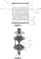
- This first embodiment 101 is an Optically-Addressed Spatial Light Modulator (OASLM), more particularly an optically addressed liquid crystal spatial light modulator 101.
- OFAM Optically-Addressed Spatial Light Modulator
- Modulator 101 is a new generation of a liquid-crystal optically addressed spatial light modulator (OASLM) that harvests incident light as a source of energy for operating without an external power supply.
- OFAM optically addressed spatial light modulator
- the liquid crystal of layer 7 is a nematic liquid crystal.
- the liquid crystal of layer 7 is a liquid crystal mixture consisting of several cyanobiphenyls with long aliphatic tails, known as "E7".
- the E7 liquid crystal used here is the classical E7 comprising the following percentages of the following molecules: 51% 25% 16% 8%
- the thickness of layer 7 is more than 1 ⁇ m, typically more than 2 ⁇ m and/or less than 100 ⁇ m, preferably from 3 to 25 microns, typically around 8 ⁇ m.
- Figures 1 and 2 illustrate the particular case comprising only one cell 456.
- Each photovoltaic cell 456 is a photovoltaic diode.
- Each photovoltaic cell 456 comprises a photosensitive layer 5 comprising electron-donating molecules D and electron accepting molecules A.
- the thickness of layer 5 is less than 500 nm, typically around 100 nm.
- electron-donating molecules D also reference number 15 on the figures
- electron accepting molecules A also reference number 14 on the figures
- the photosensitive layer 5 does not comprise any solvent for molecules A and D.
- the photosensitive layer 5 is composed only of the electron-donating molecules D and the electron accepting molecules A.
- the electron-donating molecules D are organic semiconductor molecules.
- the electron-donating molecules D comprise several copies of only one type of electron-donating molecule (here P3HT).
- the electron accepting molecules A comprise several copies of only one type of electron accepting molecule (here PCBM).
- the electron accepting molecules A, 14 are molecules of fullerene derivative [6,6]-phenyl-C 61 -butyric acid methyl ester also called PCBM (Solenne BV).
- Each photovoltaic cell 456 is arranged for spontaneous photovoltage under illumination.
- Each photovoltaic cell 456 is preferably arranged for spontaneous photovoltage of an electrical potential of at least 0.6 Volt under an illumination of 100 mW/cm 2 for at least one wavelength comprised between 350 nm and 600 nm.
- electron-donating molecules D, 15 and electron accepting molecules A, 14 are blended and form a bulk D/A heterojunction layer.
- the electron-donating molecules D are organic electron-donating molecules.
- the electron accepting molecules A are organic electron accepting molecules.
- organic matter, organic material, or organic molecule refer to carbon-based compounds preferably obtained by chemical synthesis.
- an organic molecule refers to a carbon-based molecule comprising carbon atoms linked together in rings and/or chains; these carbon atoms are preferably attached to other atoms of such elements as hydrogen, oxygen, and nitrogen.
- organic semiconductors 14, 15 allows more freedom in the design of the device 101 (flexibility, colour tuning, large area) and allows to use solution processing techniques to make the device according to the invention.
- the photovoltaic cell 456 further comprises an inside interface layer 12 in contact with the photosensitive layer 5 of this photovoltaic cell 456, this inside interface layer 12 being located between the liquid crystal layer 7 and this photosensitive layer 5.
- the inside interface layer 12 of the photovoltaic cell 456 is in contact with the liquid crystal layer 7 and is arranged for aligning the liquid crystal of the liquid crystal layer 7 at the interface between this inside interface layer 12 and the liquid crystal layer 7.
- Layer 12 has been brushed mechanically (at its face contacting layer 7) in order to be an alignment layer of the liquid crystal of layer 7.
- the photovoltaic cell 456 further comprises an outside interface layer 13 in contact with the photosensitive layer 5 of this photovoltaic cell 456, this photosensitive layer 5 being located between the liquid crystal layer 7 and this outside interface layer 13.
- the inside interface layer 12 in contact with a given photosensitive layer 5 of the same photovoltaic cell 456 and the outside interface layer 13 in contact with the same given photosensitive layer 5 of the same photovoltaic cell 456 are made of different materials.
- the modulator 101 comprises two polarizers 1, 11.
- Each polarizer 1, 11 is a WP25M-UB Ultra Broadband Wire Grid Polarizers (250 nm - 4 ⁇ m) from Thorlabs.
- Polarizers 1, 11 are crossed polarizers.
- the modulator 101 comprises two substrates 2, 10.
- Each substrate 2, 10 is a glass substrate.
- each substrate 2, 10 is more than 500 ⁇ m, typically around 1 mm.
- the modulator 101 comprises two conductive layers or electrodes 3, 9.
- Each electrode 3, 9 is a transparent conductive film.
- Each electrode 3, 9 is made of Indium tin oxide (also called ITO).
- each electrode 3, 9 is less than 200 nm, typically around 140 nm.
- the modulator 101 comprises an alignment layer 8.
- Layer 8 has been brushed mechanically (at its face contacting layer 7) in order to be an alignment layer of the liquid crystal of layer 7.
- the alignment layer 8 has a thickness less than 100 nm, typically around 30 nm.
- the liquid crystal layer 7 and the at least one photovoltaic cell 456 are comprised between the two polarizers 1, 11.
- the liquid crystal layer 7 and the at least one photovoltaic cell 456 are comprised between the two substrates 2, 10.
- the liquid crystal layer 7 and the at least one photovoltaic cell 456 are comprised between the two conductive layers or electrodes 3, 9.
- the liquid crystal layer 7 is comprised between the two alignment layers 12, 8.
- the two conductive layers or electrodes 3, 9 are comprised between the two substrates 2, 10.
- the two conductive layers or electrodes 3, 9 are comprised between the two polarizers 1, 11.
- the two substrates 2, 10 are comprised between the two polarizers 1, 11.
- At least one photovoltaic cell 456 is in contact with one of the two conductive layers or electrodes 3, 9.
- UV-curable glue mixed with calibrated microsphere (not illustrated) is used.
- the two substrates 2, 10 are glued together and a micrometric gap is formed, then the gap is filled by capillarity with liquid crystal 7. After that the gap is closed with UV-curable glue to seal the device 101.
- One among the inside interface layer 12 and the outside interface layer 13 is an electron hole conducting layer 6 arranged for a transfer of an electron hole from its contacting photosensitive layer 5 easier than a transfer of an electron from its contacting photosensitive layer 5.
- the other one among the inside interface layer 12 and the outside interface layer 13 is an electron conducting layer 4 arranged for a transfer of an electron from its contacting photosensitive layer 5 easier than a transfer of an electron hole from its contacting photosensitive layer 5.
- the inside interface layer 12 is an electron hole conducting layer 6 arranged for a transfer of electron holes from its contacting photosensitive layer 5 easier than a transfer of electrons from its contacting photosensitive layer 5.
- the electron hole conducting layer 6 is a layer of Poly(3,4-ethylenedioxythiophene)-poly(styrenesulfonate) (also called PEDOT:PSS).
- the electron hole conducting layer 6 has a thickness less than 100 nm, typically around 30 nm.
- the outside interface layer 13 is an electron conducting layer 4 arranged for a transfer of electron from its contacting photosensitive layer 5 easier than a transfer of electron holes from its contacting photosensitive layer 5.
- the electron conducting layer 4 is a layer of Polyethylenimine (also called PEI-E).
- the electron conducting layer 4 has a thickness less than 100 nm or even less than 10 nm, typically around 7 nm.
- the electron conducting layer 4 is a very thin layer (less than 10 nm thick, typically 7 nm thick) of an electrically insulating material (PEIE) but with intrinsic electrical dipoles. These dipoles make access to layer 3 difficult for electron holes, for good selectivity.
- PEIE electrically insulating material
- the interfaces between the photosensitive layer 5 and the adjacent materials 4, 6 have a considerable impact on the evolution of photo-generated charges.
- the layer 5 is comprised between two materials 4, 6, whose electronic work functions are different.
- the negative and positive charges generated in the layer 5 separate (the negative charges will accumulate preferentially at the interface with the material 4 with low work function and vice versa for the positive charges).
- the "photo-voltage" ⁇ V is equivalent to the "open circuit voltage" of a photovoltaic cell.
- the absolute value of the energy difference between the work function of the electron conducting layer 4 and the electron affinity of each electron accepting molecule of the photosensitive layer 5 contacting this outside interface layer 13 is less than or equal to 0.2 eV. This enhances the capacity of layer 4 to attract electrons from layer 5 and to conduct electrons compared to its capacity to attract electron holes form layer 5 and to conduct electron holes.
- the absolute value of the energy difference between the work function of the electron hole conducting layer 6 and the ionization potential of each electron-donating molecule of the photosensitive layer 5 contacting this inside interface layer 12 is less than or equal to 0.2 eV. This enhances the capacity of layer 6 to attract electron holes from layer 5 and to conduct electron holes compared to its capacity to attract electrons from layer 5 and to conduct electrons.
- the liquid crystal layer 7 has an electrical resistance higher than each part or layer of the photovoltaic cell 456, and even higher than each part or layer comprised between the electrodes 3, 9.
- the liquid crystal layer 7 has an electrical resistance at least two times higher than each part or layer 4, 5, 6 of the photovoltaic cell 456, and even at least two times higher than each part or layer comprised between the electrodes.
- the electrical resistance of each layer respectively 7, 4, 5, 6, 8 is measured perpendicularly to this layer respectively 7, 4, 5, 6, 8 that is parallel to the thickness of each layer respectively 7, 4, 5, 6, 8, the thickness being the smaller spatial dimension of each layer respectively 7, 4, 5, 6, 8.
- EA(A) is the electron affinity of each electron accepting molecule expressed in eV
- EA(D) is the electron affinity of each electron donating molecule expressed in eV
- IE(A) is the ionization potential of each electron accepting molecule expressed in eV
- IE(D) is the ionization potential of each electron-donating molecule expressed in eV
- the energy difference between the electron affinity and the ionization potential of each electron-donating molecule is preferably higher than or equal to 3 eV: EA(D) - IE(D) ⁇ 3 eV .
- EA(D) - IE(D) ⁇ 3 eV This allows modulator 101 to be transparent in the visible range (in its « off state »), for instance for smart windows applications. This is not the case in the particular case of the embodiment of Figure 5 .
- the energy difference between the electron affinity and the ionization potential of each electron accepting molecule is preferably higher than or equal to 3 eV: EA(A) - IE(A) ⁇ 3 eV .
- C60 derivatives such as PCBM
- the material D polymer or small molecule
- the limit of 3 eV for example for D/A mixtures where the acceptor molecules A are a derivative of C60.
- the energy difference between the electron affinity of the electron-donating molecules and the electron affinity of the electron accepting molecules is higher than or equal to 0.1 eV (EA(D) - EA(A) ⁇ 0.1 eV), preferably higher than or equal to 0.3 eV (EA(D) - EA(A) ⁇ 0.3 eV), per couple of electron-donating molecule and electron accepting molecule.
- the combination of such molecules 14, 15 allows the generation of free electrical charges in layer 5 following the absorption of UV photons in layer 5.
- the energy difference between the ionization potential of the electron-donating molecules and the ionization potential of the electron accepting molecules is higher than or equal to 0.1 eV (IE(D) - IE(A) ⁇ 0.1 eV), preferably higher than or equal to 0.3 eV (IE(D) - IE(A) ⁇ 0.3 eV), per couple of electron-donating molecule and electron accepting molecule.
- the combination of such molecules 14, 15 allows the generation of free electrical charges in layer 5 following the absorption of UV photons in layer 5.
- the energy difference between the electron affinity of the electron accepting molecules and the ionization potential of the electron-donating molecules, per couple of electron-donating molecule and electron accepting molecule respects the following equation: IE D ⁇ EA A ⁇ ⁇ V Fredericks ⁇ e + 0 , 3 where:
- the ionization potential of each electron-donating molecule is higher than or equal to 5eV. This allows enhancing the stability of the modulator 101 in the presence of oxygen or water vapor.
- the electronic affinity of each electron accepting molecule is higher than or equal to 3.5 eV. This allows enhancing the stability of the modulator 101 in the presence of oxygen or water vapor.
- the liquid crystal layer 7 and the at least one photovoltaic cell 456 are comprised between the two polarizers 1, 11.
- each photovoltaic cell 456 is less than 1 ⁇ m.
- Modulator 101 has thus a glass/ITO/ PEIE/P3HT:PCBM/PEDOT:PSS /E7/PEDOT:PSS/ITO/glass structure. Its manufacturing process is the following. Indium tin oxide (ITO) coated glass slides were used as transparent conducting electrode. The ITO coated glass slides were cleaned by successive sonication for 15 minutes each in acetone, isopropanol, deionized water. The ITO slides were then UV ozone treated prior to the organic layer deposition.
- ITO Indium tin oxide
- PEDOT:PSS (Clevios PH, Heraeus), a conductive polymer, was filtered through a 0.22 ⁇ m filter to remove aggregates, spin-coated onto the ITO coated glass slides in ambient conditions, transferred to a glovebox with an inert nitrogen atmosphere( ⁇ 1 ppm 0 2 and H 2 0), and dried for 30 min at 140°C.
- a solution of P3HT (>93% regioregular, Solaris Chem) and PCBM (Solenne BV) in chlorobenzene with a (1:1) weight ratio was prepared and stirred overnight at 60°C.
- the PEIE solution was spin-coated onto the ITO coated glass slide in ambient conditions, transferred to a glovebox with an inert nitrogen atmosphere ( ⁇ 1 ppm 0 2 and H 2 0), and dried for 10 min at 100°C.
- the photoactive layer was then spin-coated on the ITO modified substrate and dried for 10 min at 140°C.
- PEDOT:PSS Lith Generation Partnership Project
- the coated layers were then rubbed by use of a velvet cloth attached to a rotating drum in order to induce the alignment of the liquid crystal molecules along the rubbing direction in the final device.
- a mixture of adhesives UV curable glue, Loctite AA350
- spacer 7.75 ⁇ m Si0 2 Microspheres
- the adhesive was cured by exposing the substrates to UV light for 5 minutes.
- the empty cell was filled with a liquid crystal mixture known as E7 by capillarity on a hot plate at 65°C.
- the edges of the cell were sealed with an epoxy resin (Araldite) to avoid contamination.
- a summary diagram of the final cell is shown below.
- ⁇ n variable of the refractive index under illumination with 89 mW/cm 2 optical power
- the inside interface layer 12 is directly the liquid crystal layer 7.
- Layer 5 has been brushed mechanically (at its face contacting layer 7) in order to be an alignment layer of the liquid crystal of layer 7.
- the photosensitive layer 5 is thus arranged for aligning the liquid crystal of the liquid crystal layer 7 at the interface between this photosensitive layer 5 and the liquid crystal layer 7.
- the photosensitive layer 5 is hydrophobic. This cause a larger "pretilt" angle of the liquid crystal of layer 7, and thus allows a change in birefringence ⁇ n at zero bias voltage.
- This second variant of modulator 101 has thus a glass/ITO/ PEIE/P3HT:PCBM /E7/PEDOT:PSS/ITO/glass structure.
- the upper (brushed) region of layer 5 plays the role of the electron hole conducting layer 6 (but in another variant layer 13 can be the electron hole conducting layer 6 and layer 5 plays the role of the electron conducting layer 4).
- the non-zero response to 0V is an indisputable signature of the photovoltaic mode.
- the inside interface layer 12 in contact with the liquid crystal layer 7 is hydrophobic. This also allows a non-zero response to 0V.
- Curves 16, and 17 of Figure 4 clearly show that the sensitivity to the incident light is greatly improved according to the invention compared to prior art. The effect is multiplied by the superposition or multiplication of photovoltaic cells 456.
- the at least one photovoltaic cell 456 comprises, on at least one side of the liquid crystal layer 7, a superposition of a plurality of contacting photovoltaic cells 456.
- All the cell 456 are similar and comprises layer 4,13 plus layer 5 plus layer 6,12 as previously described in reference to figures 1 to 5 .
- the obtained phototension is equal or higher than 1.2 V and is sufficient to reorient the liquid crystal E7 of layer 7 that have a threshold voltage of 1V without the contribution of an external polarization, and there is a variation in birefringence in the absence of external polarization.
- the spatial light modulator 103 comprises, on each side of the liquid crystal layer 7, at least one photovoltaic cell 456.
- the obtained phototension is sufficient to reorient the liquid crystal of layer 7 without the contribution of an external polarization, and there is a variation in birefringence in the absence of external polarization.
- the utilization of an organic D/A blend (layer 5) which, when associated with appropriate interfaces 4, 6, yields a spontaneous photovoltage under illumination.
- layer 5 which, when associated with appropriate interfaces 4, 6, yields a spontaneous photovoltage under illumination.
- This differs from the response of the commonly used inorganic semiconductor thin films (e.g. amorphous Si) or previously investigated organic photosensitive layers (PVK:C60) according to prior art, for which light exposure results only in a change in electrical conductance.
- the new device according to the invention works also at zero voltage bias.
- the organic photosensitive layer is deposited from solution at room temperature, large area flexible devices may in principle be developed at low cost. According to the invention, avoiding high temperature processing should reduce the processing costs and give rise to new opportunities to apply OASLMs. The possibility according to the invention to operate at zero bias reduces the power consumption of the device and gives rise to new application opportunities.
Landscapes
- Physics & Mathematics (AREA)
- Nonlinear Science (AREA)
- Chemical & Material Sciences (AREA)
- Crystallography & Structural Chemistry (AREA)
- General Physics & Mathematics (AREA)
- Optics & Photonics (AREA)
- Mathematical Physics (AREA)
- Liquid Crystal (AREA)
- Engineering & Computer Science (AREA)
- Manufacturing & Machinery (AREA)
- Optical Modulation, Optical Deflection, Nonlinear Optics, Optical Demodulation, Optical Logic Elements (AREA)
- Photovoltaic Devices (AREA)
Priority Applications (7)
| Application Number | Priority Date | Filing Date | Title |
|---|---|---|---|
| EP17186647.8A EP3444662A1 (fr) | 2017-08-17 | 2017-08-17 | Modulateur spatial de lumière à cristaux liquides |
| KR1020207006097A KR20200039706A (ko) | 2017-08-17 | 2018-07-19 | 액정 공간 광 변조기 |
| EP18749733.4A EP3669231B1 (fr) | 2017-08-17 | 2018-07-19 | Modulateur spatial de lumière à cristaux liquides |
| JP2020509495A JP2020531901A (ja) | 2017-08-17 | 2018-07-19 | 液晶空間光変調器 |
| PCT/EP2018/069597 WO2019034359A1 (fr) | 2017-08-17 | 2018-07-19 | Modulateur spatial de lumière à cristaux liquides |
| CN201880053095.XA CN111316157A (zh) | 2017-08-17 | 2018-07-19 | 液晶空间光调制器 |
| US16/637,176 US11287705B2 (en) | 2017-08-17 | 2018-07-19 | Liquid crystal spatial light modulator |
Applications Claiming Priority (1)
| Application Number | Priority Date | Filing Date | Title |
|---|---|---|---|
| EP17186647.8A EP3444662A1 (fr) | 2017-08-17 | 2017-08-17 | Modulateur spatial de lumière à cristaux liquides |
Publications (1)
| Publication Number | Publication Date |
|---|---|
| EP3444662A1 true EP3444662A1 (fr) | 2019-02-20 |
Family
ID=59713796
Family Applications (2)
| Application Number | Title | Priority Date | Filing Date |
|---|---|---|---|
| EP17186647.8A Withdrawn EP3444662A1 (fr) | 2017-08-17 | 2017-08-17 | Modulateur spatial de lumière à cristaux liquides |
| EP18749733.4A Active EP3669231B1 (fr) | 2017-08-17 | 2018-07-19 | Modulateur spatial de lumière à cristaux liquides |
Family Applications After (1)
| Application Number | Title | Priority Date | Filing Date |
|---|---|---|---|
| EP18749733.4A Active EP3669231B1 (fr) | 2017-08-17 | 2018-07-19 | Modulateur spatial de lumière à cristaux liquides |
Country Status (6)
| Country | Link |
|---|---|
| US (1) | US11287705B2 (fr) |
| EP (2) | EP3444662A1 (fr) |
| JP (1) | JP2020531901A (fr) |
| KR (1) | KR20200039706A (fr) |
| CN (1) | CN111316157A (fr) |
| WO (1) | WO2019034359A1 (fr) |
Cited By (1)
| Publication number | Priority date | Publication date | Assignee | Title |
|---|---|---|---|---|
| WO2021013524A1 (fr) | 2019-07-19 | 2021-01-28 | Highvistec Gmbh | Dispositif à cristaux liquides adressable optiquement et électriquement |
Families Citing this family (1)
| Publication number | Priority date | Publication date | Assignee | Title |
|---|---|---|---|---|
| EP3821817A3 (fr) | 2008-11-12 | 2021-11-03 | Access Closure, Inc. | Appareil de fermeture d'une perforation vasculaire |
Citations (4)
| Publication number | Priority date | Publication date | Assignee | Title |
|---|---|---|---|---|
| WO1999067681A1 (fr) | 1998-06-24 | 1999-12-29 | Alphamicron, Inc. | Dispositif 'guest-host' a colorant dichroique d'attenuation variable de la lumiere |
| US6233027B1 (en) * | 1997-01-07 | 2001-05-15 | Canon Kabushiki Kaisha | Liquid crystal device and process for production thereof |
| US20140028957A1 (en) * | 2011-04-11 | 2014-01-30 | Yang Yang | Polarizing photovoltaic devices and applications in lcd displays and tandem solar cells |
| US20160260919A1 (en) * | 2013-11-12 | 2016-09-08 | Ppg Industries Ohio, Inc. | Photovoltaic Systems and Spray Coating Processes for Producing Photovoltaic Systems |
Family Cites Families (17)
| Publication number | Priority date | Publication date | Assignee | Title |
|---|---|---|---|---|
| JPH0343627U (fr) * | 1989-09-04 | 1991-04-24 | ||
| US5177628A (en) * | 1990-04-24 | 1993-01-05 | The University Of Colorado Foundation, Inc. | Self-powered optically addressed spatial light modulator |
| EP0583114B1 (fr) | 1992-07-30 | 2001-09-12 | Hamamatsu Photonics K.K. | Modulateur spatial de lumière adressé optiquement |
| JPH06160823A (ja) * | 1992-11-18 | 1994-06-07 | Ricoh Co Ltd | 調光用素子及び調光システム |
| JPH10301119A (ja) * | 1997-04-25 | 1998-11-13 | Hitachi Chem Co Ltd | 液晶配向膜用組成物、液晶配向膜、液晶挾持基板及び液晶表示素子 |
| JP2001133814A (ja) * | 1999-11-05 | 2001-05-18 | Fuji Xerox Co Ltd | 自己電力供給型調光素子 |
| KR20080044233A (ko) * | 2005-08-22 | 2008-05-20 | 코나르카 테크놀로지, 인코포레이티드 | 일체형 광전지를 갖는 디스플레이 |
| US7897429B2 (en) * | 2006-11-20 | 2011-03-01 | The Trustees Of Princeton University | Organic hybrid planar-nanocrystalline bulk heterojunctions |
| KR100938164B1 (ko) * | 2008-07-21 | 2010-01-21 | 한국과학기술원 | 광센서장치, 광센서장치를 포함한 디스플레이 장치,광신호를 이용한 원격입력시스템 |
| KR101604102B1 (ko) * | 2008-09-09 | 2016-03-25 | 테크니온 리서치 엔드 디벨로프먼트 화운데이션 엘티디. | 유기 반도체용의, 유도체화 풀러렌을 주성분으로 하는 도펀트 |
| EP2564247A2 (fr) * | 2010-04-27 | 2013-03-06 | The Regents Of The University Of Michigan | Dispositif d'affichage ayant des filtres de couleur plasmoniques et ayant des capacités photovoltaïques |
| WO2012060246A1 (fr) * | 2010-11-02 | 2012-05-10 | シャープ株式会社 | Dispositif d'affichage équipé d'une batterie solaire et équipement électronique |
| JP5856423B2 (ja) * | 2011-09-30 | 2016-02-09 | 株式会社東芝 | 導電材料およびこれを用いた電気素子 |
| CN102540565B (zh) * | 2012-03-20 | 2015-04-08 | 友达光电(苏州)有限公司 | 具有太阳能电池功能的彩色滤光基板及显示面板 |
| JP2013254912A (ja) * | 2012-06-08 | 2013-12-19 | Konica Minolta Inc | 有機光電変換素子およびこれを用いた太陽電池 |
| JP5940707B1 (ja) * | 2015-03-30 | 2016-06-29 | 株式会社東芝 | 電気光学装置 |
| TWI570479B (zh) * | 2015-11-12 | 2017-02-11 | 南臺科技大學 | 塗佈式太陽能電池彩色濾光片及其製法 |
-
2017
- 2017-08-17 EP EP17186647.8A patent/EP3444662A1/fr not_active Withdrawn
-
2018
- 2018-07-19 CN CN201880053095.XA patent/CN111316157A/zh active Pending
- 2018-07-19 EP EP18749733.4A patent/EP3669231B1/fr active Active
- 2018-07-19 JP JP2020509495A patent/JP2020531901A/ja active Pending
- 2018-07-19 US US16/637,176 patent/US11287705B2/en active Active
- 2018-07-19 WO PCT/EP2018/069597 patent/WO2019034359A1/fr not_active Ceased
- 2018-07-19 KR KR1020207006097A patent/KR20200039706A/ko not_active Ceased
Patent Citations (4)
| Publication number | Priority date | Publication date | Assignee | Title |
|---|---|---|---|---|
| US6233027B1 (en) * | 1997-01-07 | 2001-05-15 | Canon Kabushiki Kaisha | Liquid crystal device and process for production thereof |
| WO1999067681A1 (fr) | 1998-06-24 | 1999-12-29 | Alphamicron, Inc. | Dispositif 'guest-host' a colorant dichroique d'attenuation variable de la lumiere |
| US20140028957A1 (en) * | 2011-04-11 | 2014-01-30 | Yang Yang | Polarizing photovoltaic devices and applications in lcd displays and tandem solar cells |
| US20160260919A1 (en) * | 2013-11-12 | 2016-09-08 | Ppg Industries Ohio, Inc. | Photovoltaic Systems and Spray Coating Processes for Producing Photovoltaic Systems |
Non-Patent Citations (2)
| Title |
|---|
| L. LUCCHETTI; K. KUSHNIR; A. ZALTRON; F. SIMONI: "Liquid crystal cells based on photovoltaic substrates", EUR. OPT. SOC.-RAPID, vol. 11, 2016, pages 16007 |
| L. LUCCHETTI; K. KUSHNIR; A. ZALTRON; F. SIMONI: "Liquid crystal cells based on photovoltaic substrates", EUR. OPT. SOC.-RAPID, vol. 11, 2016, pages 16007, XP055442876 * |
Cited By (2)
| Publication number | Priority date | Publication date | Assignee | Title |
|---|---|---|---|---|
| WO2021013524A1 (fr) | 2019-07-19 | 2021-01-28 | Highvistec Gmbh | Dispositif à cristaux liquides adressable optiquement et électriquement |
| US11988913B2 (en) | 2019-07-19 | 2024-05-21 | Highvistec Gmbh | Optically and electrically addressable liquid crystal device |
Also Published As
| Publication number | Publication date |
|---|---|
| KR20200039706A (ko) | 2020-04-16 |
| EP3669231A1 (fr) | 2020-06-24 |
| EP3669231B1 (fr) | 2022-08-31 |
| US20200233248A1 (en) | 2020-07-23 |
| CN111316157A (zh) | 2020-06-19 |
| US11287705B2 (en) | 2022-03-29 |
| JP2020531901A (ja) | 2020-11-05 |
| WO2019034359A1 (fr) | 2019-02-21 |
Similar Documents
| Publication | Publication Date | Title |
|---|---|---|
| JP4915477B2 (ja) | 画像入出力装置 | |
| Shih et al. | Multilevel photonic transistor memory devices using conjugated/insulated polymer blend electrets | |
| Tseng et al. | Organic transistor memory with a charge storage molecular double-floating-gate monolayer | |
| CN101971345A (zh) | 纳米结构薄膜lcd设备 | |
| Dan et al. | Introducing chiro-optical activities in photonic synapses for neuromorphic computing and in-memory logic operations | |
| Kim et al. | Layer-by-layer assembled electrochromic films for all-solid-state electrochromic devices | |
| Lv et al. | Colorless to multicolored, fast switching, and highly stable electrochromic devices based on thermally cross-linking copolymer | |
| US9209340B2 (en) | Polarizing photovoltaic devices and applications in LCD displays and tandem solar cells | |
| Nemani et al. | Stretchable and hydrophobic electrochromic devices using wrinkled graphene and PEDOT: PSS | |
| Ho et al. | Fast photoresponsive phototransistor memory using star-shaped conjugated rod–coil molecules as a floating gate | |
| Li et al. | Photoerasable organic field-effect transistor memory based on a one-step solution-processed hybrid floating gate layer | |
| Huang et al. | High-performance organic phototransistors based on D18, a high-mobility and unipolar polymer | |
| Fall et al. | Self-powered dynamic glazing based on nematic liquid crystals and organic photovoltaic layers for smart window applications | |
| Vollbrecht et al. | Curved polar dibenzocoronene esters and imides versus their planar centrosymmetric homologs: photophysical and optoelectronic analysis | |
| Choi et al. | Polarization-dependent photoinduced bias-stress effect in single-crystal organic field-effect transistors | |
| EP3669231B1 (fr) | Modulateur spatial de lumière à cristaux liquides | |
| Yan et al. | Thermodynamics-induced injection enhanced deep-blue perovskite quantum dot LEDs | |
| Ho et al. | Discotic liquid crystals with highly ordered columnar hexagonal structure for ultraviolet light-sensitive phototransistor memory | |
| Yen et al. | Enhancing the Memory-Stretchability Property of π-Conjugated Polymers Using Pendant Arene Side Chains in Nonvolatile Transistor Memory | |
| Sefer et al. | A Novel Near‐IR Effective Pyrene‐Based Donor–Acceptor Electrochrome | |
| Rana et al. | Interface-and Temperature-Sensitive Linear Electric Field Effects on Exciton Absorption of CH3NH3PbI3 Perovskite Films | |
| DE112011105620T5 (de) | Photorefraktiver Verbundstoff | |
| Gasonoo et al. | Polymer dispersed liquid crystal for enhanced light out-coupling efficiency of organic light emitting diodes | |
| Zhou et al. | Transparent Organic Photovoltaics with Average Visible Transmission of 90% | |
| Regrettier et al. | Integrated organic donor-acceptor bulk heterojunctions for self-activated liquid crystal light modulators. |
Legal Events
| Date | Code | Title | Description |
|---|---|---|---|
| PUAI | Public reference made under article 153(3) epc to a published international application that has entered the european phase |
Free format text: ORIGINAL CODE: 0009012 |
|
| STAA | Information on the status of an ep patent application or granted ep patent |
Free format text: STATUS: THE APPLICATION HAS BEEN PUBLISHED |
|
| AK | Designated contracting states |
Kind code of ref document: A1 Designated state(s): AL AT BE BG CH CY CZ DE DK EE ES FI FR GB GR HR HU IE IS IT LI LT LU LV MC MK MT NL NO PL PT RO RS SE SI SK SM TR |
|
| AX | Request for extension of the european patent |
Extension state: BA ME |
|
| STAA | Information on the status of an ep patent application or granted ep patent |
Free format text: STATUS: THE APPLICATION IS DEEMED TO BE WITHDRAWN |
|
| 18D | Application deemed to be withdrawn |
Effective date: 20190821 |