EP3444832A1 - Commutateur électrostatique - Google Patents
Commutateur électrostatique Download PDFInfo
- Publication number
- EP3444832A1 EP3444832A1 EP17799627.9A EP17799627A EP3444832A1 EP 3444832 A1 EP3444832 A1 EP 3444832A1 EP 17799627 A EP17799627 A EP 17799627A EP 3444832 A1 EP3444832 A1 EP 3444832A1
- Authority
- EP
- European Patent Office
- Prior art keywords
- electrode pattern
- switch
- switch structure
- elastic body
- input operation
- Prior art date
- Legal status (The legal status is an assumption and is not a legal conclusion. Google has not performed a legal analysis and makes no representation as to the accuracy of the status listed.)
- Withdrawn
Links
Images






Classifications
-
- H—ELECTRICITY
- H01—ELECTRIC ELEMENTS
- H01H—ELECTRIC SWITCHES; RELAYS; SELECTORS; EMERGENCY PROTECTIVE DEVICES
- H01H36/00—Switches actuated by change of magnetic field or of electric field, e.g. by change of relative position of magnet and switch, by shielding
-
- H—ELECTRICITY
- H03—ELECTRONIC CIRCUITRY
- H03K—PULSE TECHNIQUE
- H03K17/00—Electronic switching or gating, i.e. not by contact-making and –breaking
- H03K17/94—Electronic switching or gating, i.e. not by contact-making and –breaking characterised by the way in which the control signals are generated
- H03K17/96—Touch switches
- H03K17/962—Capacitive touch switches
-
- G—PHYSICS
- G06—COMPUTING OR CALCULATING; COUNTING
- G06F—ELECTRIC DIGITAL DATA PROCESSING
- G06F3/00—Input arrangements for transferring data to be processed into a form capable of being handled by the computer; Output arrangements for transferring data from processing unit to output unit, e.g. interface arrangements
- G06F3/01—Input arrangements or combined input and output arrangements for interaction between user and computer
- G06F3/03—Arrangements for converting the position or the displacement of a member into a coded form
- G06F3/041—Digitisers, e.g. for touch screens or touch pads, characterised by the transducing means
- G06F3/0414—Digitisers, e.g. for touch screens or touch pads, characterised by the transducing means using force sensing means to determine a position
-
- G—PHYSICS
- G06—COMPUTING OR CALCULATING; COUNTING
- G06F—ELECTRIC DIGITAL DATA PROCESSING
- G06F3/00—Input arrangements for transferring data to be processed into a form capable of being handled by the computer; Output arrangements for transferring data from processing unit to output unit, e.g. interface arrangements
- G06F3/01—Input arrangements or combined input and output arrangements for interaction between user and computer
- G06F3/03—Arrangements for converting the position or the displacement of a member into a coded form
- G06F3/041—Digitisers, e.g. for touch screens or touch pads, characterised by the transducing means
- G06F3/044—Digitisers, e.g. for touch screens or touch pads, characterised by the transducing means by capacitive means
- G06F3/0443—Digitisers, e.g. for touch screens or touch pads, characterised by the transducing means by capacitive means using a single layer of sensing electrodes
-
- H—ELECTRICITY
- H01—ELECTRIC ELEMENTS
- H01H—ELECTRIC SWITCHES; RELAYS; SELECTORS; EMERGENCY PROTECTIVE DEVICES
- H01H36/00—Switches actuated by change of magnetic field or of electric field, e.g. by change of relative position of magnet and switch, by shielding
- H01H36/0006—Permanent magnet actuating reed switches
- H01H36/0013—Permanent magnet actuating reed switches characterised by the co-operation between reed switch and permanent magnet; Magnetic circuits
-
- H—ELECTRICITY
- H01—ELECTRIC ELEMENTS
- H01H—ELECTRIC SWITCHES; RELAYS; SELECTORS; EMERGENCY PROTECTIVE DEVICES
- H01H36/00—Switches actuated by change of magnetic field or of electric field, e.g. by change of relative position of magnet and switch, by shielding
- H01H36/0006—Permanent magnet actuating reed switches
- H01H36/004—Permanent magnet actuating reed switches push-button-operated, e.g. for keyboards
-
- H—ELECTRICITY
- H03—ELECTRONIC CIRCUITRY
- H03K—PULSE TECHNIQUE
- H03K17/00—Electronic switching or gating, i.e. not by contact-making and –breaking
- H03K17/94—Electronic switching or gating, i.e. not by contact-making and –breaking characterised by the way in which the control signals are generated
- H03K17/965—Switches controlled by moving an element forming part of the switch
- H03K17/975—Switches controlled by moving an element forming part of the switch using a capacitive movable element
-
- H—ELECTRICITY
- H03—ELECTRONIC CIRCUITRY
- H03K—PULSE TECHNIQUE
- H03K17/00—Electronic switching or gating, i.e. not by contact-making and –breaking
- H03K17/94—Electronic switching or gating, i.e. not by contact-making and –breaking characterised by the way in which the control signals are generated
- H03K17/96—Touch switches
- H03K2017/9602—Touch switches characterised by the type or shape of the sensing electrodes
-
- H—ELECTRICITY
- H03—ELECTRONIC CIRCUITRY
- H03K—PULSE TECHNIQUE
- H03K2217/00—Indexing scheme related to electronic switching or gating, i.e. not by contact-making or -breaking covered by H03K17/00
- H03K2217/94—Indexing scheme related to electronic switching or gating, i.e. not by contact-making or -breaking covered by H03K17/00 characterised by the way in which the control signal is generated
- H03K2217/96—Touch switches
- H03K2217/96054—Double function: touch detection combined with detection of a movable element
-
- H—ELECTRICITY
- H03—ELECTRONIC CIRCUITRY
- H03K—PULSE TECHNIQUE
- H03K2217/00—Indexing scheme related to electronic switching or gating, i.e. not by contact-making or -breaking covered by H03K17/00
- H03K2217/94—Indexing scheme related to electronic switching or gating, i.e. not by contact-making or -breaking covered by H03K17/00 characterised by the way in which the control signal is generated
- H03K2217/96—Touch switches
- H03K2217/9607—Capacitive touch switches
- H03K2217/960755—Constructional details of capacitive touch and proximity switches
-
- H—ELECTRICITY
- H03—ELECTRONIC CIRCUITRY
- H03K—PULSE TECHNIQUE
- H03K2217/00—Indexing scheme related to electronic switching or gating, i.e. not by contact-making or -breaking covered by H03K17/00
- H03K2217/94—Indexing scheme related to electronic switching or gating, i.e. not by contact-making or -breaking covered by H03K17/00 characterised by the way in which the control signal is generated
- H03K2217/96—Touch switches
- H03K2217/9607—Capacitive touch switches
- H03K2217/960755—Constructional details of capacitive touch and proximity switches
- H03K2217/96076—Constructional details of capacitive touch and proximity switches with spring electrode
-
- H—ELECTRICITY
- H03—ELECTRONIC CIRCUITRY
- H03K—PULSE TECHNIQUE
- H03K2217/00—Indexing scheme related to electronic switching or gating, i.e. not by contact-making or -breaking covered by H03K17/00
- H03K2217/94—Indexing scheme related to electronic switching or gating, i.e. not by contact-making or -breaking covered by H03K17/00 characterised by the way in which the control signal is generated
- H03K2217/96—Touch switches
- H03K2217/9607—Capacitive touch switches
- H03K2217/960755—Constructional details of capacitive touch and proximity switches
- H03K2217/96077—Constructional details of capacitive touch and proximity switches comprising an electrode which is floating
Definitions
- the present invention relates to a capacitive switch, and more particularly, to a capacitive switch for outputting electrical signals for multifunctional execution in response to changes in capacitance depending on a user touch input and a user push input.
- the present invention is directed to a capacitive switch for outputting electrical signals for multifunctional execution in response to changes in capacitance depending on a user touch input and a user push input, and a method of operating the capacitive switch.
- a capacitive switch comprising: a switch structure having a first electrode pattern; a substrate having a second electrode pattern and an integrated circuit unit; and an elastic body interposed between the switch structure and the substrate, wherein the integrated circuit unit generates a first output signal by detecting a change in capacitance caused by a user touch input operation through the first electrode pattern, the elastic body, and the second electrode pattern, and generates a second output signal by detecting a change in capacitance caused by a user push input operation.
- a portion of the first electrode pattern extends laterally from an upper surface inside the switch structure or extends from the upper surface inside the switch structure to a lower surface along a side surface inside the switch structure.
- the switch structure comprises: a cap portion; a support portion configured to support the cap portion; and a guide portion configured to guide a moving path of the support portion according to the user push input operation.
- the first electrode pattern is formed on the support portion, and a portion of the first electrode pattern extends laterally from an upper surface of the support portion or extends from the upper surface of the support portion to a lower surface along a side surface of the support portion.
- the first electrode pattern is formed on the support portion and the guide portion, and a portion of the first electrode pattern extends from an upper surface of the support portion to a lower surface of the guide portion along a side surface and a lower surface of the support portion.
- a portion of the second electrode pattern is formed on the elastic body and faces the portion of the first electrode pattern formed on a lower surface of the guide portion with a gap.
- a portion of the first electrode pattern is formed on a bottom surface of the switch structure, and another portion of the first electrode pattern is formed on the elastic body and contacts the portion of the first electrode pattern formed on the bottom surface of the switch structure.
- the user touch input operation does not involve a physical change of the elastic body, and the user push input operation involves a physical change of the elastic body.
- the first electrode pattern is formed directly on the switch structure by a laser direct structuring process or a multiple injection process.
- the capacitive switch further comprises a cover member covering at least a portion of an exposed surface of the first electrode pattern.
- a capacitive switch according to embodiments of the present invention may reduce structural complexity because there is no need to implement a contact and may prevent the durability from being reduced due to contact wear.
- the capacitive switch according to embodiments of the present invention may be manufactured in a simplified process without being restricted by the shape by using a laser direct structuring process.
- inventive concept may be variously modified and have various example embodiments, so that specific example embodiments will be illustrated in the drawings and described in the detailed description. However, this does not limit the inventive concept to specific example embodiments, and it should be understood that the inventive concept covers all the modifications, equivalents and replacements included within the idea and technical scope of the inventive concept.
- each processes may be performed by hardware such as a processor, a micro processor, a micro controller, a central processing unit (CPU), a graphics processing unit (GPU), an accelerated Processing unit (APU), a digital signal processor (DSP), an application specific integrated circuit (ASIC), and a field programmable gate array (FPGA) or a combination of hardware and software in a system.
- hardware such as a processor, a micro processor, a micro controller, a central processing unit (CPU), a graphics processing unit (GPU), an accelerated Processing unit (APU), a digital signal processor (DSP), an application specific integrated circuit (ASIC), and a field programmable gate array (FPGA) or a combination of hardware and software in a system.
- CPU central processing unit
- GPU graphics processing unit
- APU accelerated Processing unit
- DSP digital signal processor
- ASIC application specific integrated circuit
- FPGA field programmable gate array
- components in the specification are distinguished in terms of primary functions of the components. That is, two or more components to be described below may be provided to be combined to one component or one component may be provided to be divided into two or more components for each more subdivided function.
- each of the respective components to be described below may additionally perform some or all functions among functions which other components take charge of in addition to a primary function which each component takes charge of and some functions among the primary functions which the respective components take charge of are exclusively charged by other components to be performed, of course.
- FIG. 1 is a view for explaining a principle of the operation of a capacitive switch, according to embodiments of the present invention.
- a capacitive switch 10 may include a switch structure 100, an elastic body 200, and a substrate 300.
- the switch structure 100 is a portion where a user touch input according to a user's touch or a user push input according to a user's push is performed.
- the switch structure 100 may be implemented as an injection molding material of a polymer, and may have a three-dimensional (3D) shape in which at least one surface is planar or curved.
- the switch structure 100 may be implemented as an integral structure (see FIGS. 2 and 3 ) or a combined structure (see FIGS. 4 to 9 ) in which a plurality of components are combined.
- the switch structure 100 may have a shape in which at least a portion of a bottom surface opposite to an upper surface of the elastic body 200 is opened and an inner space is provided.
- the switch structure 100 may include first electrode patterns 150-1, 150-2, and 150-3.
- the first electrode patterns 150-1, 150-2, and 150-3 may be exposed inside the switch structure 100 and may extend laterally from an upper surface inside the switch structure 100, or may extend from the upper surface inside the switch structure 100 to a lower surface along a side surface.
- a portion 150-1 of the first electrode patterns may be formed on the upper surface inside the switch structure 100
- another portion 150-2 of the first electrode patterns may be formed on the side surface inside the switch structure 100
- the other portion 150-3 of the first electrode patterns may be formed on the lower surface inside the switch structure 100.
- the first electrode patterns 150-1, 150-2, and 150-3 may be implemented in a floating state to detect a touch input operation or a push input operation of a user.
- the first electrode patterns 150-1, 150-2, and 150-3 may be formed directly on the switch structure 100 by a laser direct structuring process.
- the laser direct structuring process may be performed by a process in which a support material is formed from a material including a non-conductive and chemically stable metal complex, and a portion of the support material is exposed to a laser beam such as an ultraviolet (UV) laser or an excimer laser to release a chemical bond of the metal complex to expose a metal seed and then the support material is metalized to form a conductive structure at an area of the support material exposed to the laser beam.
- a laser beam such as an ultraviolet (UV) laser or an excimer laser to release a chemical bond of the metal complex to expose a metal seed and then the support material is metalized to form a conductive structure at an area of the support material exposed to the laser beam.
- the process of forming the first electrode patterns 150-1, 150-2, and 150-3 is not limited to the laser direct structuring process, and the first electrode patterns 150-1, 150-2, and 150-3 may be formed through various patterning processes.
- the first electrode patterns 150-1, 150-2, and 150-3 may be formed by a patterning process such as double injection, multiple injection, etc., in which injection molding and conductive pattern formation are performed at one time.
- the cover member may include the same material as that of the switch structure 100, but is not limited thereto.
- the cover member may include a material different from that of the switch structure 100, or may have a multi-layer structure. Durability of the first electrode patterns 150-1, 150-2, and 150-3 may be improved by the cover member.
- the elastic body 200 may be interposed between the switch structure 100 and the substrate 300.
- the elastic body 200 is interposed between the switch structure 100 and the substrate 300 so that the elastic body 200 is contracted when a user applies a push input operation to the switch structure 100 and then restored to its original shape by elasticity when the push input operation is completed, thereby restoring the switch structure 100 to its original position.
- the elastic body 200 may include an elastic material (e.g., rubber) as an insulating material.
- an elastic material e.g., rubber
- the substrate 300 may include a printed circuit board (PCB), a flexible PCB (FPCB), or the like.
- PCB printed circuit board
- FPCB flexible PCB
- the substrate 300 may include a second electrode pattern 310 and an integrated circuit unit 400.
- the second electrode pattern 310 may have a shape corresponding to the first electrode patterns 150-1, 150-2, and 150-3, but the present invention is not limited thereto.
- the second electrode pattern 310 may be implemented in various shapes and sizes.
- the integrated circuit unit 400 may generate a first output signal by detecting a change in capacitance caused by a user touch input operation, and may generate a second output signal by detecting a change in capacitance caused by a user push input operation.
- a first state STATE1 denotes a state where no user input operation is performed
- a second state STATE2 denotes a state where a user touch input operation is performed
- a third state STATE3 denotes a state where a user push input operation is performed.
- the user touch input operation does not involve a physical change of the elastic body 200, and the user push input operation may involve a physical change of the elastic body 200.
- the capacitance between the first electrode patterns 150-1, 150-2, and 150-3 and the second electrode pattern 310 has a first value C0 in the first state STATE1
- the capacitance has a second value C1 by the user touch input operation in second state STATE2
- the capacitance has a third value C2 by the user push input operation in the third state STATE3.
- the integrated circuit unit 400 may detect a change in capacitance between the first state STATE 1, the second state STATE2, and the third state STATE3 to distinguish the user touch input operation from the user push input operation, and may perform a corresponding function by outputting an output signal corresponding to each of the user touch input operation and the user push input operation.
- the second state STATE2 and the third state STATE3 may be implemented as sequential user input operations.
- the second state STATE2 may be implemented as a preliminary input to activate the third state STATE3.
- the integrated circuit unit 400 may provide guidance information about the user push input operation through a visual or auditory device.
- a user may perform the push input operation according to provided guidance information.
- the integrated circuit unit 400 may perform a predetermined specific function.
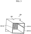
- FIGS. 2 and 3 are views of a portion of a capacitive switch according to an embodiment of the present invention.
- FIGS. 2 and 3 show a portion of a capacitive switch 10A according to an embodiment for convenience of explanation.
- the switch structure 100 may be integrally formed.
- first electrode patterns 150-1A, 150-2A, and 150-3A may be formed over an upper surface, a side surface, and a lower surface inside the switch structure 100.
- a portion 150-1A (hereinafter referred to as a first portion) of the first electrode patterns may be formed on the upper surface inside the switch structure 100.
- the first portion 150-1A has a shape covering the entire upper surface inside the switch structure 100, but is not limited thereto.
- a light emitting device is provided on the substrate 300
- a light transmitting region may be formed on the switch structure 100
- the first portion 150-1A may have a shape having a vacant region corresponding to the light transmitting region.
- Another portion 150-2A (hereinafter referred to as a second portion) of the first electrode patterns may be connected to the first portion 150-1A and may be formed on a side surface inside the switch structure 100.
- a plurality of second portions 150-2A are formed on side surfaces facing each other inside the switch structure 100, respectively, but the present invention is not limited thereto.
- the second portions 150-2A may be formed on one side surface inside the switch structure 100. It is understood that the second portion 150-2A may have various widths, thicknesses, and shapes.
- the other portion 150-3A (hereinafter referred to as a third portion) of the first electrode patterns may be connected to the second portion 150-2A and may be formed on the lower surface of the switch structure 100.
- the third portion 150-3A may be formed to cover a bottom surface of at least a portion of side walls defining an inner space of the switch structure 100, and may be connected to the second portion 150-2A formed on an outer surface of the side walls.
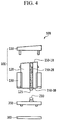
- FIGS. 4 and 5 are views of a capacitive switch according to another embodiment of the present invention.
- a capacitive switch 10B may include the switch structure 100, the elastic body 200, and the substrate 300.
- the switch structure 100 may be implemented as a combined structure in which a plurality of components are combined.
- the switch structure 100 may include a cap portion 110, a support portion 120, and a guide portion 130.
- the cap portion 110 which is a portion that a user touches for a user touch input operation or a user push input operation, may be formed separately from the support portion 120 that supports the cap portion 110 and combined with the support portion 120.
- the support portion 120 may have a square pipe structure having an empty space therein. However, the support portion 120 is not limited thereto.
- the support portion 120 may have a pipe structure of various shapes such as a circular shape with a vertical cross section of hollow shape in an axial direction.
- the guide portion 130 may be coupled to a side surface of the support portion 120 or may be integrally formed with the support portion 120.
- the guide portion 130 may be coupled with an external structure to guide an up and down path of the support portion 120.
- first electrode patterns 150-1B, 150-2B, and 150-3B may be formed on the support portion 120.
- a portion 150-1B of the first electrode patterns may be formed on an upper surface of the support portion 120
- another portion 150-2B of the first electrode patterns may be formed on a side surface of the support portion 120
- the other portion 150-3B of the first electrode patterns may be formed on a lower surface of the support portion 120.
- the elastic body 200 is formed with a protrusion 210 to be in contact with a protrusion 125 of the support portion 120.
- the elastic body 200 is contracted according to a user's push input operation and then restored to its original shape by elasticity when the push input operation is completed, thereby restoring the switch structure 100 to its original position.
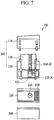
- FIGS. 6 and 7 are views of a capacitive switch according to another embodiment of the present invention.
- a portion 150-3C of first electrode patterns 150-1C, 150-2C, and 150-3C may extend to the guide portion 130.
- the first electrode patterns 150-1C, 150-2C, and 150-3C may extend from an upper surface of the support portion 120 to a lower surface of the guide portion 130 along a side surface and a lower surface of the support portion 120.
- an extended portion 310' of the second electrode pattern 310 may be formed in a region corresponding to a region where the second electrode pattern 310 is formed on the substrate 300 in the elastic body 200, and may be electrically connected to the second electrode pattern 310 formed on the substrate 300.
- the extended portion 310' of the second electrode pattern 310 may face a portion 150-3C of the first electrode patterns formed on the lower surface of the guide portion 130 with a gap. Meanwhile, the extended portion 310' of the second electrode pattern 310 may be spaced apart from the portion 150-3C of the first electrode patterns even when a user's switch push input operation is performed.
- FIGS. 8 and 9 are views of a capacitive switch according to another embodiment of the present invention.
- a portion 150-3D of first electrode patterns may be formed on the lower surface of the guide portion 130 and the protrusion 125 of the support portion 120.
- An extended portion 150' of the first electrode patterns may be formed on the elastic body 200.
- the extended portion 150' of the first electrode patterns may further be formed on the protrusion 210 of the elastic body 200 and the extended portion 150' of the first electrode patterns formed on the protrusion 210 of the elastic body 200 may be electrically connected to the portion 150-3D of the first electrode patterns formed on the protrusion 125 of the support portion 120.
- FIGS. 10 and 11 are views of a capacitive switch according to another embodiment of the present invention.
- a portion of an extended portion 310" of a second electrode pattern may be formed in the elastic body 200 in a shape corresponding to a bottom surface of the guide portion 130 and the other portion of the extended portion 310" of the second electrode pattern may be formed in the shape of a ring on an outer edge of the protrusion 210 excluding an upper surface of the protrusion 210 and may be connected to each other.
- a position and a width of the ring shape may vary.
- a portion of the extended portion 310" of the second electrode pattern formed in the ring shape may have high durability because the portion of the extended portion 310" of the second electrode pattern does not contact a first electrode pattern 150-3E formed on the protrusion 125 of the support portion 120 even when a user push input is performed.
- the portion of the extended portion 310" of the second electrode pattern formed in the ring shape may be formed so as to be as close as possible to the first electrode pattern 150-3E formed on the protrusion 125 of the support portion 120 without contacting the first electrode pattern 150-3E.
- a portion formed on a bottom surface of the protrusion 125 of the support portion 120 and a portion formed on the bottom surface of the guide portion 130 may be connected to each other.
- FIG. 12 is a view of an example in which an additional pattern is formed on the substrate shown in FIGS. 4 to 11 .
- a ground pattern 312 may be formed together with the second electrode pattern 310 on the substrate 300.
- the ground pattern 312 may be formed on an outer edge of the second electrode pattern 310 so as not to contact the second electrode pattern 310.
- the ground pattern 312 formed on the substrate 300 may prevent external noise, thereby preventing malfunction of the capacitive switches 10A to 10E due to external noise.
Landscapes
- Engineering & Computer Science (AREA)
- General Engineering & Computer Science (AREA)
- Theoretical Computer Science (AREA)
- Human Computer Interaction (AREA)
- Physics & Mathematics (AREA)
- General Physics & Mathematics (AREA)
- Switches That Are Operated By Magnetic Or Electric Fields (AREA)
Applications Claiming Priority (3)
| Application Number | Priority Date | Filing Date | Title |
|---|---|---|---|
| KR20160060339 | 2016-05-17 | ||
| KR1020160074228A KR101905851B1 (ko) | 2016-05-17 | 2016-06-15 | 정전식 스위치 |
| PCT/KR2017/005067 WO2017200270A1 (fr) | 2016-05-17 | 2017-05-16 | Commutateur électrostatique |
Publications (2)
| Publication Number | Publication Date |
|---|---|
| EP3444832A1 true EP3444832A1 (fr) | 2019-02-20 |
| EP3444832A4 EP3444832A4 (fr) | 2019-12-11 |
Family
ID=60810963
Family Applications (1)
| Application Number | Title | Priority Date | Filing Date |
|---|---|---|---|
| EP17799627.9A Withdrawn EP3444832A4 (fr) | 2016-05-17 | 2017-05-16 | Commutateur électrostatique |
Country Status (5)
| Country | Link |
|---|---|
| US (1) | US10680610B2 (fr) |
| EP (1) | EP3444832A4 (fr) |
| JP (1) | JP6771096B2 (fr) |
| KR (1) | KR101905851B1 (fr) |
| CN (1) | CN109155218B (fr) |
Cited By (5)
| Publication number | Priority date | Publication date | Assignee | Title |
|---|---|---|---|---|
| EP3905529A1 (fr) * | 2020-04-29 | 2021-11-03 | Hilti Aktiengesellschaft | Machine-outil guidée à la main |
| US12088290B2 (en) | 2020-04-29 | 2024-09-10 | Hilti Aktiengesellschaft | Hand-held machine tool and related method |
| US12176894B2 (en) | 2020-04-29 | 2024-12-24 | Hilti Aktiengesellschaft | Hand-held machine tool and related method |
| US12556182B2 (en) | 2020-04-29 | 2026-02-17 | Hilti Aktiengesellschaft | Hand-held machine tool |
| US12592698B2 (en) | 2020-04-29 | 2026-03-31 | Hilti Aktiengesellschaft | Hand-held machine tool |
Families Citing this family (5)
| Publication number | Priority date | Publication date | Assignee | Title |
|---|---|---|---|---|
| KR102075578B1 (ko) * | 2018-07-26 | 2020-02-11 | 주식회사 시노펙스 | 이중 탄성체 구조를 갖는 포스 센서 스위치 |
| KR102134805B1 (ko) * | 2018-07-30 | 2020-07-16 | 주식회사 시노펙스 | 클릭감을 제공하는 포스 센서 스위치 |
| DE112020003126T5 (de) * | 2019-06-28 | 2022-05-05 | Alps Alpine Co., Ltd. | Eingabevorrichtung |
| KR102343091B1 (ko) * | 2021-06-16 | 2021-12-28 | 채학수 | 방향지시등용 레그 조작장치 및 이를 설치한 개인형 동력이동장치 |
| CN118098855B (zh) * | 2024-04-26 | 2024-08-09 | 基合半导体(宁波)有限公司 | 电容感应式按键、设备、移动距离检测方法及存储介质 |
Family Cites Families (16)
| Publication number | Priority date | Publication date | Assignee | Title |
|---|---|---|---|---|
| NO20003974L (no) * | 2000-02-18 | 2001-08-20 | Ziad Badarneh | Manöverinnretning |
| JP4303059B2 (ja) * | 2003-08-08 | 2009-07-29 | 株式会社東海理化電機製作所 | 操作スイッチ及び車両用エンジンの始動・停止システム |
| DE102004044378A1 (de) * | 2004-09-10 | 2006-03-30 | Valeo Schalter Und Sensoren Gmbh | Schaltereinheit |
| JP2008289058A (ja) * | 2007-05-21 | 2008-11-27 | Tokai Rika Co Ltd | スイッチ装置 |
| US7829812B2 (en) * | 2007-07-03 | 2010-11-09 | Sony Ericsson Mobile Communications Ab | Input device and an electronic device comprising an input device |
| US9654104B2 (en) * | 2007-07-17 | 2017-05-16 | Apple Inc. | Resistive force sensor with capacitive discrimination |
| JP4646340B2 (ja) * | 2008-09-03 | 2011-03-09 | 昌徳 水島 | 入力装置 |
| KR101068444B1 (ko) * | 2008-12-19 | 2011-09-28 | 에이디반도체(주) | 정전용량 터치 스위치의 터치캡 |
| US8872771B2 (en) * | 2009-07-07 | 2014-10-28 | Apple Inc. | Touch sensing device having conductive nodes |
| DE102009032634A1 (de) * | 2009-07-10 | 2011-01-13 | Trw Automotive Electronics & Components Gmbh | Tastschalter mit kapazitiver Tastenerkennung |
| JP5292221B2 (ja) * | 2009-08-21 | 2013-09-18 | アルプス電気株式会社 | 静電容量センサ付きプッシュスイッチおよびそれを用いた入力装置 |
| WO2011130755A2 (fr) * | 2010-04-14 | 2011-10-20 | Frederick Johannes Bruwer | Construction de commutateur de circuit de détection capacitif en fonction de la pression |
| KR20140124918A (ko) * | 2013-04-02 | 2014-10-28 | 김한주 | 레이저 직접 구조화 공정용 조성물 |
| US20140354577A1 (en) * | 2013-05-28 | 2014-12-04 | Ingar Hanssen | Multi-State Capacitive Button |
| KR20160041199A (ko) | 2014-10-07 | 2016-04-18 | 손동일 | 다채널 스위치 모듈 |
| JP6246692B2 (ja) * | 2014-10-10 | 2017-12-13 | 信越ポリマー株式会社 | タッチセンサおよびその製造方法 |
-
2016
- 2016-06-15 KR KR1020160074228A patent/KR101905851B1/ko active Active
-
2017
- 2017-05-16 EP EP17799627.9A patent/EP3444832A4/fr not_active Withdrawn
- 2017-05-16 US US16/302,395 patent/US10680610B2/en active Active
- 2017-05-16 CN CN201780030813.7A patent/CN109155218B/zh active Active
- 2017-05-16 JP JP2019513723A patent/JP6771096B2/ja active Active
Cited By (7)
| Publication number | Priority date | Publication date | Assignee | Title |
|---|---|---|---|---|
| EP3905529A1 (fr) * | 2020-04-29 | 2021-11-03 | Hilti Aktiengesellschaft | Machine-outil guidée à la main |
| WO2021219433A1 (fr) * | 2020-04-29 | 2021-11-04 | Hilti Aktiengesellschaft | Machine-outil portative |
| US20230173653A1 (en) * | 2020-04-29 | 2023-06-08 | Hilti Aktiengesellschaft | Hand-held machine tool |
| US12088290B2 (en) | 2020-04-29 | 2024-09-10 | Hilti Aktiengesellschaft | Hand-held machine tool and related method |
| US12176894B2 (en) | 2020-04-29 | 2024-12-24 | Hilti Aktiengesellschaft | Hand-held machine tool and related method |
| US12556182B2 (en) | 2020-04-29 | 2026-02-17 | Hilti Aktiengesellschaft | Hand-held machine tool |
| US12592698B2 (en) | 2020-04-29 | 2026-03-31 | Hilti Aktiengesellschaft | Hand-held machine tool |
Also Published As
| Publication number | Publication date |
|---|---|
| US10680610B2 (en) | 2020-06-09 |
| US20190312578A1 (en) | 2019-10-10 |
| KR101905851B1 (ko) | 2018-10-11 |
| JP6771096B2 (ja) | 2020-10-21 |
| EP3444832A4 (fr) | 2019-12-11 |
| CN109155218B (zh) | 2020-06-30 |
| KR20170129583A (ko) | 2017-11-27 |
| JP2019515482A (ja) | 2019-06-06 |
| CN109155218A (zh) | 2019-01-04 |
Similar Documents
| Publication | Publication Date | Title |
|---|---|---|
| EP3444832A1 (fr) | Commutateur électrostatique | |
| US11723276B2 (en) | Method for manufacturing an actuator switch | |
| JP4554651B2 (ja) | タッチパネル入力装置 | |
| KR101226354B1 (ko) | 공유 전극 패턴 전계 효과 센서 및 이를 구비한 조이스틱 | |
| CN113994308B (zh) | 输入装置以及输入系统 | |
| KR102233011B1 (ko) | 스위치 장치 | |
| JP5770324B1 (ja) | 操作検出装置 | |
| JP5804309B2 (ja) | タッチセンサ | |
| KR101032995B1 (ko) | 전자제품용 신호입력장치 | |
| CN110023890B (zh) | 触摸传感器误感测防止构造以及包含其的电子设备 | |
| KR20120058134A (ko) | 택트 스위치 | |
| KR102570402B1 (ko) | 곡면형 터치 스위치 및 그 제조방법 | |
| EP2541771B1 (fr) | Procédé de fabrication d'un élément de commutation électrique | |
| KR102930138B1 (ko) | 전자 기기 | |
| KR20180001448A (ko) | 터치 입력 장치 | |
| US9838009B2 (en) | Switch with user feedback | |
| US9501173B2 (en) | Input device | |
| KR102081726B1 (ko) | 스위치 | |
| WO2017200270A1 (fr) | Commutateur électrostatique | |
| WO2016006216A1 (fr) | Commutateur et dispositif d'entrée l'utilisant | |
| JP6230065B2 (ja) | 入力装置 | |
| JPWO2018207486A1 (ja) | シフト装置 | |
| KR20170104723A (ko) | 지문 센서 장치 | |
| JP2013149475A (ja) | スイッチ装置 |
Legal Events
| Date | Code | Title | Description |
|---|---|---|---|
| STAA | Information on the status of an ep patent application or granted ep patent |
Free format text: STATUS: THE INTERNATIONAL PUBLICATION HAS BEEN MADE |
|
| PUAI | Public reference made under article 153(3) epc to a published international application that has entered the european phase |
Free format text: ORIGINAL CODE: 0009012 |
|
| STAA | Information on the status of an ep patent application or granted ep patent |
Free format text: STATUS: REQUEST FOR EXAMINATION WAS MADE |
|
| 17P | Request for examination filed |
Effective date: 20181116 |
|
| AK | Designated contracting states |
Kind code of ref document: A1 Designated state(s): AL AT BE BG CH CY CZ DE DK EE ES FI FR GB GR HR HU IE IS IT LI LT LU LV MC MK MT NL NO PL PT RO RS SE SI SK SM TR |
|
| AX | Request for extension of the european patent |
Extension state: BA ME |
|
| RIN1 | Information on inventor provided before grant (corrected) |
Inventor name: KIM, JUNG KYU Inventor name: LEE, YONG HEE Inventor name: SEO, TAE IN |
|
| DAV | Request for validation of the european patent (deleted) | ||
| DAX | Request for extension of the european patent (deleted) | ||
| REG | Reference to a national code |
Ref country code: DE Ref legal event code: R079 Free format text: PREVIOUS MAIN CLASS: H01H0036000000 Ipc: H03K0017975000 |
|
| A4 | Supplementary search report drawn up and despatched |
Effective date: 20191113 |
|
| RIC1 | Information provided on ipc code assigned before grant |
Ipc: H03K 17/975 20060101AFI20191107BHEP Ipc: H03K 17/96 20060101ALI20191107BHEP |
|
| STAA | Information on the status of an ep patent application or granted ep patent |
Free format text: STATUS: EXAMINATION IS IN PROGRESS |
|
| 17Q | First examination report despatched |
Effective date: 20211011 |
|
| 17Q | First examination report despatched |
Effective date: 20211022 |
|
| STAA | Information on the status of an ep patent application or granted ep patent |
Free format text: STATUS: THE APPLICATION IS DEEMED TO BE WITHDRAWN |
|
| 18D | Application deemed to be withdrawn |
Effective date: 20230613 |