EP3444890B1 - Commutateur haute fréquence - Google Patents
Commutateur haute fréquence Download PDFInfo
- Publication number
- EP3444890B1 EP3444890B1 EP18785220.7A EP18785220A EP3444890B1 EP 3444890 B1 EP3444890 B1 EP 3444890B1 EP 18785220 A EP18785220 A EP 18785220A EP 3444890 B1 EP3444890 B1 EP 3444890B1
- Authority
- EP
- European Patent Office
- Prior art keywords
- transistor
- terminal
- frequency switch
- transmitted
- state
- Prior art date
- Legal status (The legal status is an assumption and is not a legal conclusion. Google has not performed a legal analysis and makes no representation as to the accuracy of the status listed.)
- Active
Links
Images


Classifications
-
- H—ELECTRICITY
- H04—ELECTRIC COMMUNICATION TECHNIQUE
- H04B—TRANSMISSION
- H04B1/00—Details of transmission systems, not covered by a single one of groups H04B3/00 - H04B13/00; Details of transmission systems not characterised by the medium used for transmission
- H04B1/38—Transceivers, i.e. devices in which transmitter and receiver form a structural unit and in which at least one part is used for functions of transmitting and receiving
- H04B1/40—Circuits
- H04B1/44—Transmit/receive switching
-
- H—ELECTRICITY
- H03—ELECTRONIC CIRCUITRY
- H03K—PULSE TECHNIQUE
- H03K17/00—Electronic switching or gating, i.e. not by contact-making and –breaking
- H03K17/51—Electronic switching or gating, i.e. not by contact-making and –breaking characterised by the components used
- H03K17/56—Electronic switching or gating, i.e. not by contact-making and –breaking characterised by the components used by the use, as active elements, of semiconductor devices
- H03K17/687—Electronic switching or gating, i.e. not by contact-making and –breaking characterised by the components used by the use, as active elements, of semiconductor devices the devices being field-effect transistors
- H03K17/693—Switching arrangements with several input- or output-terminals, e.g. multiplexers, distributors
-
- H—ELECTRICITY
- H03—ELECTRONIC CIRCUITRY
- H03K—PULSE TECHNIQUE
- H03K17/00—Electronic switching or gating, i.e. not by contact-making and –breaking
- H03K17/94—Electronic switching or gating, i.e. not by contact-making and –breaking characterised by the way in which the control signals are generated
- H03K17/945—Proximity switches
- H03K17/95—Proximity switches using a magnetic detector
- H03K17/952—Proximity switches using a magnetic detector using inductive coils
- H03K17/9537—Proximity switches using a magnetic detector using inductive coils in a resonant circuit
Definitions
- the present invention relates to a high-frequency switch.
- a system such as a radar uses an common antenna for the transmission and the reception.
- a transmitter and receiver module including a high-frequency switch is defined by a transmitting circuit and a receiving circuit.
- Input and output terminals of the antenna, an input terminal of the receiving circuit, and an output terminal of the transmitting circuit are connected to one another by a circulator.
- the high-frequency switch has its input terminal connected to the circulator.
- the high-frequency switch also has a first output terminal connected to an LNA (Low Noise Amplifier), and a second output terminal connected to a termination.
- LNA Low Noise Amplifier
- the high-frequency switch serves a function of allowing the signal to pass between the input terminal and the first output terminal, such that the received signal is output to the LNA at a stage following the high-frequency switch.
- the high-frequency switch serves a function of allowing the signal to pass between the input terminal and the second output terminal, such that the signal leaking via the circulator or the transmitted signal reflected from the antenna is output to the termination connected to the second output terminal, with the result that the LNA at the following stage is protected from the transmitted signal.
- AGC automatic gain control
- a high-frequency switch having a circuit configuration illustrated in FIG. 1 of Patent Literature 1 all of the transistors are in an off-state when a signal is received, and all of the transistors are in an on-state when a signal is transmitted.
- an on-resistance of a transistor 2c is small enough to be considered as being short-circuited when the high-frequency switch is viewed from an input/output terminal 1c connected to an LNA.
- total reflection from the high-frequency switch as the high-frequency switch is viewed from the input/output terminal 1c connected to the LNA occurs, which causes degradation of receiving characteristics or an unstable operation of the LNA.
- the high-frequency switch having the circuit configuration illustrated in FIG. 1 of Patent Literature 1 is difficult to use as an AGC, and a separate AGC circuit is required to be provided at a stage preceding the LNA.
- Patent Literature 1 Japanese Patent Application Laid-open No. 2013-98771
- Patent Literature 1 when a conventional high-frequency switch illustrated in FIG. 1 of Patent Literature 1 is used as an AGC, the total reflection as viewed from a first output terminal connected to an LNA to the high-frequency switch occurs, which causes degradation of characteristics related to reception or an unstable operation of the LNA.
- the present invention has been achieved in view of the above, and an object of the present invention is to provide a high-frequency switch that can reduce reflection as viewed from a terminal connected to which an LNA.
- a high-frequency switch includes 1: a first transistor having a drain terminal connected to an input terminal, and a source terminal connected to a first output terminal; a second transistor having a drain terminal connected to the first output terminal; a third transistor having a drain terminal connected to a source terminal of the second transistor, and a grounded source terminal; a resistor having one end connected to a connection between the source terminal of the second transistor and the drain terminal of the third transistor, and another end grounded; a switching circuit connected between the input terminal and a second output terminal, the switching circuit being switchable between a state in which the switching circuit allows passage of a transmitted/received signal between the input terminal and the second output terminal and a state in which the switching circuit cuts off the transmitted/received signal; and a control unit to control the first transistor, the second transistor, the third transistor, and the switching circuit.
- the control unit brings the switching circuit into the state in which the switching circuit cuts off the transmitted/received signal, places the first transistor and the third transistor in an on-state, and places the second transistor in an off-state.
- the control unit brings the switching circuit into the state in which the switching circuit allows the passage of the transmitted/received signal, places the first transistor and the third transistor in an off-state, and places the second transistor in an on-state.
- the present invention achieves an effect of providing the high-frequency switch that can reduce the reflection as viewed from the terminal connected to the LNA.
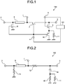
- FIG. 1 is a circuit diagram illustrating a high-frequency switch 100 according to a first embodiment of the present invention.
- the high-frequency switch 100 includes transistors 7, 8, 9, and 10, a resistor 11, a transmission line 6, and a control unit 101.
- the transistors 7, 8, 9, and 10 are field effect transistors.
- the transistors 7, 8, 9, and 10 can be transistors other than field effect transistors.
- the control unit 101 is a control circuit that controls gate voltages of the transistors 7, 8, 9, and 10.
- an input terminal 1 is connected to an antenna (not illustrated).
- An output terminal 3 that is a first output terminal is connected to an LNA (not illustrated).
- An output terminal 2 that is a second output terminal is connected to a termination (not illustrated).
- a drain terminal of the transistor 7 that is a first transistor is connected to a connection between the input terminal 1 and the one end of the transmission line 6.
- a source terminal of the transistor 7 is connected to the output terminal 3.
- a drain terminal of the transistor 8 is connected to a connection between the other end of the transmission line 6 and the output terminal 2.
- a source terminal of the transistor 8 is grounded.
- a drain terminal of the transistor 9 that is a second transistor is connected to a connection between the source terminal of the transistor 7 and the output terminal 3.
- a source terminal of the transistor 9 is connected to a drain terminal of the transistor 10.
- the drain terminal of the transistor 10 that is a third transistor is connected to the source terminal the transistor 9.
- a source terminal of the transistor 10 is grounded.
- One end of the resistor 11 is connected to a connection between the source terminal of the transistor 9 and the drain terminal of the transistor 10. The other end of the resistor 11 is grounded.
- the transmission line 6 and the transistor 8 define a switching circuit connected between the input terminal 1 and the output terminal 2.
- the configuration of the switching circuit is not limited to one defined by the transmission line 6 and the transistor 8, as long as the switching circuit is a circuit switchable between a state in which the switching circuit allows passage of a transmitted/received signal between the input terminal 1 and the output terminal 2 and a state in which the switching circuit cuts off the transmitted/received signal.
- the control unit 101 controls the switching circuit to bring the switching circuit into one of the state in which the switching circuit allows the transmitted/received signal to pass between the input terminal 1 and the output terminal 2 or the state in which the switching circuit cuts off the transmitted/received signal. Specifically, the control unit 101 controls a gate voltage of the transistor 8, thereby switching the state of the switching circuit.
- a control terminal 4 is connected to a gate terminal of each of the transistors 7, 8, and 10.
- a control terminal 5 is connected to a gate terminal of the transistor 9.
- the control terminal 4 and the control terminal 5 are connected to the control unit 101.
- the control terminal places the transistor in an on-state by applying a gate voltage equal to or higher than a pinch-off voltage to a gate terminal of the transistor, and places the transistor in an off-state by applying a gate voltage lower than the pinch-off voltage thereto. Since the transistor in the on-state can be equivalently considered as a resistor, the transistor in the on-state is hereinafter referred to as "on-resistance". Since the transistor in the off-state can be equivalently considered as a capacitor, the transistor in the off-sate is hereinafter referred to as "off-capacitance".
- the control unit 101 of the high-frequency switch 100 illustrated in FIG. 1 controls the gate voltages via the control terminal 4 and the control terminal 5, so that the transistors 7, 8, and 10 are placed in the on-state and the transistor 9 is placed in the off-state.
- the switching circuit described above becomes the state in which the switching circuit cuts off a transmitted/received signal.
- the control unit 101 controls the gate voltages via the control terminal 4 and the control terminal 5, thereby placing the transistors 7, 8, and 10 in the off-state and placing the transistor 9 in the on-state.
- the switching circuit described above becomes the state in which the switching circuit allows the passage of a transmitted/received signal.
- control unit 101 In addition to switching between the transmission and the reception, when it is determined that power of a received signal may become excessive for an LNA at the time of the reception without the AGC operation, the control unit 101 also switches each of the transistors 7, 8, 9, and 10 between the on-state and the off-state in the manner described above in order to perform the AGC operation.
- FIG. 2 is an equivalent circuit diagram of the high-frequency switch 100 according to the first embodiment at the time of the reception without the AGC operation.
- the transmission line 6 is set to have an electrical length of 90° at a center frequency of a transmitted/received signal.
- an on-resistance 13 of the transistor 8 is sufficiently small as compared with an impedance of the termination connected to the output terminal 2, the connected portion of the transmission line 6 to the output terminal 2 can be considered as being short-circuited and an impedance of the transmission line 6 as viewed from the input terminal 1 can be approximated to be infinite.
- An impedance of an off-capacitance 14 of the transistor 9 is set to be sufficiently high near the center frequency of the transmitted/received signal, such that a received signal is transmitted from the input terminal 1 to the output terminal 3.
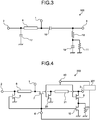
- FIG. 3 is an equivalent circuit diagram of the high-frequency switch 100 according to the first embodiment at the time of the reception with the AGC operation and the transmission.
- an impedance of an off-capacitance 16 of the transistor 7 is set to be sufficiently high near a center frequency of a transmitted/received signal, the blockade between the input terminal 1 and the output terminal 3 occurs.
- an impedance of an off-capacitance 17 of the transistor 8 is set to be sufficiently high near the center frequency of the transmitted/received signal, thereby allowing passage of a transmitted signal from the input terminal 1 to the output terminal 2 at the time of the transmission.
- the transmitted signal is transmitted from the input terminal 1 to the output terminal 2.
- a received signal is sufficiently attenuated and is transmitted to the output terminal 3.
- an off-capacitance 19 of the transistor 10 is set to have a sufficiently high impedance near the center frequency of the transmitted/received signal, an impedance of the high-frequency switch 100 as viewed from the output terminal 3 appears to be terminated with a combined resistance of an on-resistance 18 of the transistor 9 and the resistor 11.
- a value of the resistor 11 is therefore determined to make the combined resistance of the on-resistance 18 and the resistor 11 equal to a characteristic impedance of an LNA, such that reflection by the high-frequency switch 100 as viewed from the output terminal 3 can be reduced.
- the impedance of the high-frequency switch 100 as viewed from the output terminal 3 connected to an LNA appears to be terminated with the combined resistance of the on-resistance 18 of the transistor 9 and the resistor 11. This results in an effect that reflection by the high-frequency switch 100 as viewed from the output terminal 3 connected to the LNA is not total reflection, but is reduced.
- the high-frequency switch 100 of the first embodiment namely, signals from the output terminal 3 to the high-frequency switch 100 at the time of the transmission and at the time of reception are reflected to the same degree, and the reflection of the signal by the high-frequency switch 100 as viewed from the output terminal 3 can be reduced.
- the high-frequency switch 100 of the first embodiment enables stable operation of the following LNA connected thereto, at the time of the reception with the AGC operation, thereby improving the receiving characteristics. Further, it is not necessary to additionally provide the high-frequency switch 100 with an additional AGC circuit. As a result, the high-frequency switch 100 is downsized due to the reduction in the scale of the circuit of the high-frequency switch 100.
- FIG. 4 is a circuit diagram illustrating a high-frequency switch 200 according to a second embodiment of the present invention.
- the high-frequency switch 200 includes a transistor 20 that is a fourth transistor, and a transmission line 21. Further, the high-frequency switch 200 includes a control unit 201 in place of the control unit 101. A description of the same elements of the high-frequency switch 200 as those of the high-frequency switch 100 is omitted, and a description is made below as to mainly the respects in which the high-frequency switch 200 differs from the high-frequency switch 100.
- a source terminal of the transistor 7 is connected to one end of the transmission line 21.
- the other end of the transmission line 21 is connected to the output terminal 3. That is, the source terminal of the transistor 7 is connected to the output terminal 3 via the transmission line 21.
- the transmission line 21 is set to have an electrical length of 90° at a center frequency of a transmitted/received signal.
- a drain terminal of the transistor 20 is connected to a connection between the source terminal of the transistor 7 and the transmission line 21.
- a source terminal of the transistor 20 is grounded.
- a drain terminal of the transistor 9 is connected to a connection between the other end of the transmission line 21 and the output terminal 3.
- a control terminal 50 is connected to gate terminals of the transistors 9 and 20. The control terminal 4 and the control terminal 50 are connected to the control unit 201.
- the control unit 201 of the high-frequency switch 200 illustrated in FIG. 4 controls gate voltages via the control terminal 4 and the control terminal 50, so that the transistors 7, 8, and 10 are placed in the on-state and the transistors 9 and 20 are placed in the off-state.
- a switching circuit defined by the transmission line 6 and the transistor 8 becomes a state in which the switching circuit cuts off a transmitted/received signal.
- the control unit 201 controls the gate voltages via the control terminal 4 and the control terminal 50, thereby placing the transistors 7, 8, and 10 in the off-state and placing the transistors 9 and 20 in the on-state.
- the switching circuit defined by the transmission line 6 and the transistor 8 becomes the state in which the switching circuit allows passage of a transmitted/received signal.
- control unit 201 In addition to switching between the transmission and the reception, when it is determined that power of a received signal may become excessive for an LNA at the time of the reception without the AGC operation, the control unit 201 also switches between the on-state and the off-state of each of the transistors 7, 8, 9, 10, and 20 in the manner described above in order to perform the AGC operation.
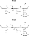
- FIG. 5 is an equivalent circuit diagram of the high-frequency switch 200 according to the second embodiment at the time of the reception without the AGC operation.
- the transmission line 6 is set to have an electrical length of 90° at a center frequency of a transmitted/received signal.
- the on-resistance 13 of the transistor 8 is sufficiently small as compared with an impedance of the termination connected to the output terminal 2, the connected portion of the transmission line 6 to the output terminal 2 can be considered as being short-circuited and an impedance of the transmission line 6 as viewed from the input terminal 1 can be approximated to be infinite. As a result, a received signal transmitted from the input terminal 1 toward the output terminal 2 is cut off.
- FIG. 6 is an equivalent circuit diagram of the high-frequency switch 200 according to the second embodiment at the time of the reception with the AGC operation and transmission.
- An impedance of each of the off-capacitance 16 of the transistor 7 and the off-capacitance 17 of the transistor 8 is set to be sufficiently high near a center frequency of a transmitted/received signal.
- a transmitted signal leaking from the off-capacitance 16 of the transistor 7 is reflected as an on-resistance 29 of the transistor 20 is small enough to be considered as being short-circuited.
- the amount of isolation is improved as compared with the blockade achieved only by the off-capacitance 16 of the transistor 7 of the high-frequency switch 100 according to the first embodiment.
- the transmission line 21 of the high-frequency switch 200 is set to have an electrical length of 90° at a center frequency of a transmitted/received signal, and an input impedance of the transmission line 21 as viewed from the input terminal 1 can be approximated to be infinite.
- an impedance of the off-capacitance 19 of the transistor 10 is set to be sufficiently high near the center frequency of the transmitted/received signal, an impedance of the high-frequency switch 200 as viewed from the output terminal 3 appears to be terminated with a combined resistance of the on-resistance 18 of the transistor 9 and the resistor 11.
- the high-frequency switch 200 according to the second embodiment can achieve the same advantageous effects as those produced by the high-frequency switch 100 according to the first embodiment, and can achieve an effect that the amount of isolation is improved by the on-resistance 29 of the transistor 20 at the time of the transmission or at the time of the reception with the AGC operation.
- FIG. 7 is a circuit diagram illustrating a high-frequency switch 300 according to a third embodiment of the present invention.
- the high-frequency switch 300 includes an inductor 32 and a resistor 33.
- a description of same elements of the high-frequency switch 300 as those of the high-frequency switch 100 is omitted, and a description is made below as to mainly the respects in which the high-frequency switch 300 differs from the high-frequency switch 100.
- each of the inductor 32 and the resistor 33 is connected to a drain terminal of the transistor 7, and the other end of each of the inductor 32 and the resistor 33 is connected to a source terminal of the transistor 7. That is, each of the inductor 32 and the resistor 33 has its both ends connected to the drain terminal and the source terminal of the transistor 7.
- the control unit 101 of the high-frequency switch 300 illustrated in FIG. 7 controls gate voltages via the control terminal 4 and the control terminal 5, so that the transistors 7, 8, and 10 are placed in the on-state and the transistor 9 is placed in the off-state.
- the control unit 101 controls the gate voltages via the control terminal 4 and the control terminal 5, thereby placing the transistors 7, 8, and 10 in the off-state and placing the transistor 9 in the on-state.
- FIG. 8 is an equivalent circuit diagram of the high-frequency switch 300 according to the third embodiment at the time of the signal reception without the AGC operation.
- the transmission line 6 is set to have an electrical length of 90° at a center frequency of a transmitted/received signal.
- the on-resistance 13 of the transistor 8 is sufficiently small as compared with an impedance of the termination connected to the output terminal 2, the connected portion of the transmission line 6 to the output terminal 2 can be considered as being short-circuited and an impedance of the transmission line 6 as viewed from the input terminal 1 can be approximated to be infinite.
- a received signal transmitted from the input terminal 1 to the output terminal 2 is cut off.
- an impedance of the off-capacitance 14 of the transistor 9 is set to be sufficiently high near the center frequency of the transmitted/received signal, and the received signal is transmitted from the input terminal 1 to the output terminal 3. Since the on-resistance 12 of the transistor 7 is sufficiently small, an influence of loss by the inductor 32 and the resistor 33 connected in parallel to each other can be ignored.
- FIG. 9 is an equivalent circuit diagram of the high-frequency switch 300 according to the third embodiment at the time of the reception with the AGC operation and the transmission.
- the off-capacitance 16 of the transistor 7 and the inductor 32 are set to cause parallel resonance at a center frequency of a transmitted/received signal, the blockade between the input terminal 1 and the output terminal 3 occurs.
- an impedance of the off-capacitance 17 of the transistor 8 is set to be sufficiently high near the center frequency of the transmitted/received signal, a transmitted signal at the time of the transmission is transmitted from the input terminal 1 to the output terminal 2. Further, a received signal at the time of the reception with the AGC operation is sufficiently attenuated and is transmitted to the output terminal 3.
- the resistor 33 connected in parallel to a resonant circuit defined by the off-capacitance 16 of the transistor 7 and the inductor 32 has a function of lowering a Q factor of this resonant circuit to make isolation characteristics wider. Since an impedance of the resonant circuit defined by the off-capacitance 16 and the inductor 32 can be approximated to be infinite and the off-capacitance 19 of the transistor 10 is set to have a sufficiently high impedance near the center frequency of the transmitted/received signal, an impedance of the high-frequency switch 300 as viewed from the output terminal 3 appears to be terminated with a combined resistance of the on-resistance 18 of the transistor 9 and the resistor 11.
- the high-frequency switch 300 according to the third embodiment can achieve the same effects as those produced by the high-frequency switch 100 according to the first embodiment, and can achieve an effect that the amount of isolation is improved by the resonant circuit defined by the off-capacitance 16 of the transistor 7 and the inductor 32. Since the high-frequency switch 300 does not require the transmission line 21 used in the high-frequency switch 200 according to the second embodiment, the high-frequency switch 300 has advantages that the scale of the circuit of the high-frequency switch 300 is downsized and the line loss is reduced, as compared with the high-frequency switch 200.
Landscapes
- Engineering & Computer Science (AREA)
- Computer Networks & Wireless Communication (AREA)
- Signal Processing (AREA)
- Electronic Switches (AREA)
- Transceivers (AREA)
- Waveguide Switches, Polarizers, And Phase Shifters (AREA)
Claims (4)
- Commutateur haute fréquence (100 ; 200 ; 300) comprenant :un premier transistor (7) ayant une borne de drain connectée à une borne d'entrée (1) et une borne de source connectée à une première borne de sortie (3) ;un deuxième transistor (9) ayant une borne de drain connectée à la première borne de sortie ;un troisième transistor (10) ayant une borne de drain connectée à une borne de source du deuxième transistor et une borne de source mise à la terre ;une résistance (11) ayant une extrémité connectée à une connexion entre la borne de source du deuxième transistor et la borne de drain du troisième transistor, et une autre extrémité mise à la terre ;un circuit de commutation (6,8) connecté entre la borne d'entrée et une seconde borne de sortie, le circuit de commutation pouvant être commuté entre un état dans lequel le circuit de commutation permet le passage d'un signal transmis/reçu entre la borne d'entrée et la seconde borne de sortie et un état dans lequel le circuit de commutation coupe le signal transmis/reçu ; etune unité de commande (101) pour commander le premier transistor, le deuxième transistor, le troisième transistor et le circuit de commutation, dans lequelà un moment de réception sans opération de commande de gain automatique, l'unité de commande met le circuit de commutation dans l'état dans lequel le circuit de commutation coupe le signal transmis/reçu, met le premier et le troisième transistor à l'état passant, et met le deuxième transistor à l'état bloqué, etau moment de l'émission et de la réception avec l'opération de commande de gain automatique, l'unité de commande met le circuit de commutation dans l'état dans lequel le circuit de commutation permet le passage du signal transmis/reçu, met le premier transistor et le troisième transistor dans un état bloqué, et met le deuxième transistor dans un état passant.
- Commutateur haute fréquence selon la revendication 1, dans lequel
la borne de source du premier transistor est connectée à la première borne de sortie via une ligne de transmission (21) qui est réglée pour avoir une longueur électrique de 90° à une fréquence centrale du signal transmis/reçu, et
le commutateur haute fréquence comprend en outre un quatrième transistor (20) ayant une borne de drain connectée à une connexion entre la borne de source du premier transistor et la ligne de transmission, et une borne de source mise à la terre. - Commutateur haute fréquence selon la revendication 1, comprenant en outre un inducteur (32) ayant les deux extrémités connectées à la borne de drain du premier transistor et à la borne de source du premier transistor, dans lequel
une capacité de coupure (16) du premier transistor et de l'inductance provoque une résonance parallèle à une fréquence centrale du signal transmis/reçu. - Commutateur haute fréquence selon la revendication 3, comprenant en outre une résistance (33) dont les deux extrémités sont connectées à la borne de drain du premier transistor et à la borne de source du premier transistor.
Applications Claiming Priority (2)
| Application Number | Priority Date | Filing Date | Title |
|---|---|---|---|
| JP2017077619 | 2017-04-10 | ||
| PCT/JP2018/008348 WO2018190034A1 (fr) | 2017-04-10 | 2018-03-05 | Commutateur haute fréquence |
Publications (3)
| Publication Number | Publication Date |
|---|---|
| EP3444890A1 EP3444890A1 (fr) | 2019-02-20 |
| EP3444890A4 EP3444890A4 (fr) | 2019-04-10 |
| EP3444890B1 true EP3444890B1 (fr) | 2019-09-11 |
Family
ID=63792973
Family Applications (1)
| Application Number | Title | Priority Date | Filing Date |
|---|---|---|---|
| EP18785220.7A Active EP3444890B1 (fr) | 2017-04-10 | 2018-03-05 | Commutateur haute fréquence |
Country Status (4)
| Country | Link |
|---|---|
| US (1) | US10700682B2 (fr) |
| EP (1) | EP3444890B1 (fr) |
| JP (1) | JP6651056B2 (fr) |
| WO (1) | WO2018190034A1 (fr) |
Families Citing this family (1)
| Publication number | Priority date | Publication date | Assignee | Title |
|---|---|---|---|---|
| US11955961B2 (en) * | 2021-10-12 | 2024-04-09 | Electronics And Telecommunications Research Institute | Switch circuit for ultra-high frequency band |
Family Cites Families (4)
| Publication number | Priority date | Publication date | Assignee | Title |
|---|---|---|---|---|
| JP2004172729A (ja) * | 2002-11-18 | 2004-06-17 | Hitachi Metals Ltd | アンテナ送受信切替え回路 |
| JP2012074890A (ja) * | 2010-09-28 | 2012-04-12 | Sumitomo Electric Device Innovations Inc | スイッチ及びスイッチの制御方法 |
| JP5822660B2 (ja) * | 2011-11-01 | 2015-11-24 | 三菱電機株式会社 | 高周波スイッチ |
| KR20130077432A (ko) * | 2011-12-29 | 2013-07-09 | 한국전자통신연구원 | 자동 이득 조절 귀환 증폭기 |
-
2018
- 2018-03-05 WO PCT/JP2018/008348 patent/WO2018190034A1/fr not_active Ceased
- 2018-03-05 US US16/499,622 patent/US10700682B2/en active Active
- 2018-03-05 EP EP18785220.7A patent/EP3444890B1/fr active Active
- 2018-03-05 JP JP2019512382A patent/JP6651056B2/ja not_active Expired - Fee Related
Non-Patent Citations (1)
| Title |
|---|
| None * |
Also Published As
| Publication number | Publication date |
|---|---|
| EP3444890A4 (fr) | 2019-04-10 |
| JP6651056B2 (ja) | 2020-02-19 |
| US10700682B2 (en) | 2020-06-30 |
| WO2018190034A1 (fr) | 2018-10-18 |
| EP3444890A1 (fr) | 2019-02-20 |
| JPWO2018190034A1 (ja) | 2019-07-11 |
| US20200044651A1 (en) | 2020-02-06 |
Similar Documents
| Publication | Publication Date | Title |
|---|---|---|
| US8306481B2 (en) | Single pole multi throw switch | |
| US7920833B2 (en) | Radio front end with resonant transmit/receive switch | |
| US8416032B2 (en) | Semiconductor switch, transceiver, transmitter, and receiver | |
| CN106330218A (zh) | 一种接收机及可降低噪声系数且增加隔离度的agc控制系统 | |
| US8909171B2 (en) | RF antenna switch circuit, high frequency antenna component, and mobile communication device | |
| US20020177417A1 (en) | Transmit/receive switch for an RF transceiver | |
| CN104953996B (zh) | 一种高隔离度射频开关电路 | |
| US9882601B1 (en) | Power amplifier with ground switch for transmit/receive functionality | |
| KR100633442B1 (ko) | 마이크로파 에스피디티 스위치 | |
| US20150381168A1 (en) | High frequency switching circuit | |
| EP3444890B1 (fr) | Commutateur haute fréquence | |
| US11563410B1 (en) | Systems and methods for multi-band power amplifiers | |
| US10187108B2 (en) | Low loss antenna switch | |
| US8538368B1 (en) | Dynamic power limiter circuit | |
| EP1772964A1 (fr) | Circuit de commutation haute fréquence | |
| US11722134B2 (en) | Radio frequency communication system and radio frequency switch thereof | |
| CN117176098A (zh) | 限幅电路和无线收发装置 | |
| KR20150073274A (ko) | 고주파 스위치 | |
| US6392608B2 (en) | Device for decreasing the number of antennas on a combat vehicle | |
| EP1739827B1 (fr) | Récepteur radiofréquence comportant un limiteur et méthodes correspondantes | |
| US20050118962A1 (en) | Receiver reuse switching | |
| KR101567472B1 (ko) | 송수신 스위치가 없는 양방향 증폭장치 | |
| CN110768638A (zh) | 单电压控制电调衰减电路和稳幅装置 | |
| KR101539909B1 (ko) | 고주파 스위치 | |
| US9343807B2 (en) | Antenna system for receiving and transmitting wireless signals |
Legal Events
| Date | Code | Title | Description |
|---|---|---|---|
| STAA | Information on the status of an ep patent application or granted ep patent |
Free format text: STATUS: THE INTERNATIONAL PUBLICATION HAS BEEN MADE |
|
| PUAI | Public reference made under article 153(3) epc to a published international application that has entered the european phase |
Free format text: ORIGINAL CODE: 0009012 |
|
| STAA | Information on the status of an ep patent application or granted ep patent |
Free format text: STATUS: REQUEST FOR EXAMINATION WAS MADE |
|
| 17P | Request for examination filed |
Effective date: 20181113 |
|
| AK | Designated contracting states |
Kind code of ref document: A1 Designated state(s): AL AT BE BG CH CY CZ DE DK EE ES FI FR GB GR HR HU IE IS IT LI LT LU LV MC MK MT NL NO PL PT RO RS SE SI SK SM TR |
|
| AX | Request for extension of the european patent |
Extension state: BA ME |
|
| A4 | Supplementary search report drawn up and despatched |
Effective date: 20190314 |
|
| RIC1 | Information provided on ipc code assigned before grant |
Ipc: H01P 1/15 20060101AFI20190307BHEP Ipc: H04B 1/44 20060101ALI20190307BHEP |
|
| GRAP | Despatch of communication of intention to grant a patent |
Free format text: ORIGINAL CODE: EPIDOSNIGR1 |
|
| STAA | Information on the status of an ep patent application or granted ep patent |
Free format text: STATUS: GRANT OF PATENT IS INTENDED |
|
| INTG | Intention to grant announced |
Effective date: 20190514 |
|
| GRAS | Grant fee paid |
Free format text: ORIGINAL CODE: EPIDOSNIGR3 |
|
| GRAA | (expected) grant |
Free format text: ORIGINAL CODE: 0009210 |
|
| STAA | Information on the status of an ep patent application or granted ep patent |
Free format text: STATUS: THE PATENT HAS BEEN GRANTED |
|
| DAV | Request for validation of the european patent (deleted) | ||
| DAX | Request for extension of the european patent (deleted) | ||
| AK | Designated contracting states |
Kind code of ref document: B1 Designated state(s): AL AT BE BG CH CY CZ DE DK EE ES FI FR GB GR HR HU IE IS IT LI LT LU LV MC MK MT NL NO PL PT RO RS SE SI SK SM TR |
|
| REG | Reference to a national code |
Ref country code: GB Ref legal event code: FG4D |
|
| REG | Reference to a national code |
Ref country code: CH Ref legal event code: EP |
|
| REG | Reference to a national code |
Ref country code: AT Ref legal event code: REF Ref document number: 1179686 Country of ref document: AT Kind code of ref document: T Effective date: 20190915 |
|
| REG | Reference to a national code |
Ref country code: DE Ref legal event code: R096 Ref document number: 602018000622 Country of ref document: DE Ref country code: IE Ref legal event code: FG4D |
|
| REG | Reference to a national code |
Ref country code: NL Ref legal event code: MP Effective date: 20190911 |
|
| REG | Reference to a national code |
Ref country code: LT Ref legal event code: MG4D |
|
| PG25 | Lapsed in a contracting state [announced via postgrant information from national office to epo] |
Ref country code: BG Free format text: LAPSE BECAUSE OF FAILURE TO SUBMIT A TRANSLATION OF THE DESCRIPTION OR TO PAY THE FEE WITHIN THE PRESCRIBED TIME-LIMIT Effective date: 20191211 Ref country code: FI Free format text: LAPSE BECAUSE OF FAILURE TO SUBMIT A TRANSLATION OF THE DESCRIPTION OR TO PAY THE FEE WITHIN THE PRESCRIBED TIME-LIMIT Effective date: 20190911 Ref country code: SE Free format text: LAPSE BECAUSE OF FAILURE TO SUBMIT A TRANSLATION OF THE DESCRIPTION OR TO PAY THE FEE WITHIN THE PRESCRIBED TIME-LIMIT Effective date: 20190911 Ref country code: HR Free format text: LAPSE BECAUSE OF FAILURE TO SUBMIT A TRANSLATION OF THE DESCRIPTION OR TO PAY THE FEE WITHIN THE PRESCRIBED TIME-LIMIT Effective date: 20190911 Ref country code: NO Free format text: LAPSE BECAUSE OF FAILURE TO SUBMIT A TRANSLATION OF THE DESCRIPTION OR TO PAY THE FEE WITHIN THE PRESCRIBED TIME-LIMIT Effective date: 20191211 Ref country code: LT Free format text: LAPSE BECAUSE OF FAILURE TO SUBMIT A TRANSLATION OF THE DESCRIPTION OR TO PAY THE FEE WITHIN THE PRESCRIBED TIME-LIMIT Effective date: 20190911 |
|
| PG25 | Lapsed in a contracting state [announced via postgrant information from national office to epo] |
Ref country code: AL Free format text: LAPSE BECAUSE OF FAILURE TO SUBMIT A TRANSLATION OF THE DESCRIPTION OR TO PAY THE FEE WITHIN THE PRESCRIBED TIME-LIMIT Effective date: 20190911 Ref country code: ES Free format text: LAPSE BECAUSE OF FAILURE TO SUBMIT A TRANSLATION OF THE DESCRIPTION OR TO PAY THE FEE WITHIN THE PRESCRIBED TIME-LIMIT Effective date: 20190911 Ref country code: RS Free format text: LAPSE BECAUSE OF FAILURE TO SUBMIT A TRANSLATION OF THE DESCRIPTION OR TO PAY THE FEE WITHIN THE PRESCRIBED TIME-LIMIT Effective date: 20190911 Ref country code: LV Free format text: LAPSE BECAUSE OF FAILURE TO SUBMIT A TRANSLATION OF THE DESCRIPTION OR TO PAY THE FEE WITHIN THE PRESCRIBED TIME-LIMIT Effective date: 20190911 Ref country code: GR Free format text: LAPSE BECAUSE OF FAILURE TO SUBMIT A TRANSLATION OF THE DESCRIPTION OR TO PAY THE FEE WITHIN THE PRESCRIBED TIME-LIMIT Effective date: 20191212 |
|
| REG | Reference to a national code |
Ref country code: AT Ref legal event code: MK05 Ref document number: 1179686 Country of ref document: AT Kind code of ref document: T Effective date: 20190911 |
|
| PG25 | Lapsed in a contracting state [announced via postgrant information from national office to epo] |
Ref country code: PT Free format text: LAPSE BECAUSE OF FAILURE TO SUBMIT A TRANSLATION OF THE DESCRIPTION OR TO PAY THE FEE WITHIN THE PRESCRIBED TIME-LIMIT Effective date: 20200113 Ref country code: PL Free format text: LAPSE BECAUSE OF FAILURE TO SUBMIT A TRANSLATION OF THE DESCRIPTION OR TO PAY THE FEE WITHIN THE PRESCRIBED TIME-LIMIT Effective date: 20190911 Ref country code: EE Free format text: LAPSE BECAUSE OF FAILURE TO SUBMIT A TRANSLATION OF THE DESCRIPTION OR TO PAY THE FEE WITHIN THE PRESCRIBED TIME-LIMIT Effective date: 20190911 Ref country code: RO Free format text: LAPSE BECAUSE OF FAILURE TO SUBMIT A TRANSLATION OF THE DESCRIPTION OR TO PAY THE FEE WITHIN THE PRESCRIBED TIME-LIMIT Effective date: 20190911 Ref country code: NL Free format text: LAPSE BECAUSE OF FAILURE TO SUBMIT A TRANSLATION OF THE DESCRIPTION OR TO PAY THE FEE WITHIN THE PRESCRIBED TIME-LIMIT Effective date: 20190911 Ref country code: AT Free format text: LAPSE BECAUSE OF FAILURE TO SUBMIT A TRANSLATION OF THE DESCRIPTION OR TO PAY THE FEE WITHIN THE PRESCRIBED TIME-LIMIT Effective date: 20190911 |
|
| PG25 | Lapsed in a contracting state [announced via postgrant information from national office to epo] |
Ref country code: SK Free format text: LAPSE BECAUSE OF FAILURE TO SUBMIT A TRANSLATION OF THE DESCRIPTION OR TO PAY THE FEE WITHIN THE PRESCRIBED TIME-LIMIT Effective date: 20190911 Ref country code: SM Free format text: LAPSE BECAUSE OF FAILURE TO SUBMIT A TRANSLATION OF THE DESCRIPTION OR TO PAY THE FEE WITHIN THE PRESCRIBED TIME-LIMIT Effective date: 20190911 Ref country code: IS Free format text: LAPSE BECAUSE OF FAILURE TO SUBMIT A TRANSLATION OF THE DESCRIPTION OR TO PAY THE FEE WITHIN THE PRESCRIBED TIME-LIMIT Effective date: 20200224 Ref country code: CZ Free format text: LAPSE BECAUSE OF FAILURE TO SUBMIT A TRANSLATION OF THE DESCRIPTION OR TO PAY THE FEE WITHIN THE PRESCRIBED TIME-LIMIT Effective date: 20190911 |
|
| REG | Reference to a national code |
Ref country code: DE Ref legal event code: R097 Ref document number: 602018000622 Country of ref document: DE |
|
| PLBE | No opposition filed within time limit |
Free format text: ORIGINAL CODE: 0009261 |
|
| STAA | Information on the status of an ep patent application or granted ep patent |
Free format text: STATUS: NO OPPOSITION FILED WITHIN TIME LIMIT |
|
| PG2D | Information on lapse in contracting state deleted |
Ref country code: IS |
|
| PG25 | Lapsed in a contracting state [announced via postgrant information from national office to epo] |
Ref country code: DK Free format text: LAPSE BECAUSE OF FAILURE TO SUBMIT A TRANSLATION OF THE DESCRIPTION OR TO PAY THE FEE WITHIN THE PRESCRIBED TIME-LIMIT Effective date: 20190911 Ref country code: IS Free format text: LAPSE BECAUSE OF FAILURE TO SUBMIT A TRANSLATION OF THE DESCRIPTION OR TO PAY THE FEE WITHIN THE PRESCRIBED TIME-LIMIT Effective date: 20200112 |
|
| 26N | No opposition filed |
Effective date: 20200615 |
|
| REG | Reference to a national code |
Ref country code: DE Ref legal event code: R119 Ref document number: 602018000622 Country of ref document: DE |
|
| PG25 | Lapsed in a contracting state [announced via postgrant information from national office to epo] |
Ref country code: MC Free format text: LAPSE BECAUSE OF FAILURE TO SUBMIT A TRANSLATION OF THE DESCRIPTION OR TO PAY THE FEE WITHIN THE PRESCRIBED TIME-LIMIT Effective date: 20190911 |
|
| REG | Reference to a national code |
Ref country code: BE Ref legal event code: MM Effective date: 20200331 |
|
| PG25 | Lapsed in a contracting state [announced via postgrant information from national office to epo] |
Ref country code: LU Free format text: LAPSE BECAUSE OF NON-PAYMENT OF DUE FEES Effective date: 20200305 |
|
| PG25 | Lapsed in a contracting state [announced via postgrant information from national office to epo] |
Ref country code: DE Free format text: LAPSE BECAUSE OF NON-PAYMENT OF DUE FEES Effective date: 20201001 Ref country code: FR Free format text: LAPSE BECAUSE OF NON-PAYMENT OF DUE FEES Effective date: 20200331 Ref country code: IE Free format text: LAPSE BECAUSE OF NON-PAYMENT OF DUE FEES Effective date: 20200305 |
|
| PG25 | Lapsed in a contracting state [announced via postgrant information from national office to epo] |
Ref country code: BE Free format text: LAPSE BECAUSE OF NON-PAYMENT OF DUE FEES Effective date: 20200331 |
|
| REG | Reference to a national code |
Ref country code: CH Ref legal event code: PL |
|
| PG25 | Lapsed in a contracting state [announced via postgrant information from national office to epo] |
Ref country code: LI Free format text: LAPSE BECAUSE OF NON-PAYMENT OF DUE FEES Effective date: 20210331 Ref country code: CH Free format text: LAPSE BECAUSE OF NON-PAYMENT OF DUE FEES Effective date: 20210331 |
|
| PGFP | Annual fee paid to national office [announced via postgrant information from national office to epo] |
Ref country code: GB Payment date: 20220127 Year of fee payment: 5 |
|
| PG25 | Lapsed in a contracting state [announced via postgrant information from national office to epo] |
Ref country code: TR Free format text: LAPSE BECAUSE OF FAILURE TO SUBMIT A TRANSLATION OF THE DESCRIPTION OR TO PAY THE FEE WITHIN THE PRESCRIBED TIME-LIMIT Effective date: 20190911 Ref country code: MT Free format text: LAPSE BECAUSE OF FAILURE TO SUBMIT A TRANSLATION OF THE DESCRIPTION OR TO PAY THE FEE WITHIN THE PRESCRIBED TIME-LIMIT Effective date: 20190911 Ref country code: CY Free format text: LAPSE BECAUSE OF FAILURE TO SUBMIT A TRANSLATION OF THE DESCRIPTION OR TO PAY THE FEE WITHIN THE PRESCRIBED TIME-LIMIT Effective date: 20190911 |
|
| PG25 | Lapsed in a contracting state [announced via postgrant information from national office to epo] |
Ref country code: MK Free format text: LAPSE BECAUSE OF FAILURE TO SUBMIT A TRANSLATION OF THE DESCRIPTION OR TO PAY THE FEE WITHIN THE PRESCRIBED TIME-LIMIT Effective date: 20190911 |
|
| PG25 | Lapsed in a contracting state [announced via postgrant information from national office to epo] |
Ref country code: IT Free format text: LAPSE BECAUSE OF NON-PAYMENT OF DUE FEES Effective date: 20190911 |
|
| PG25 | Lapsed in a contracting state [announced via postgrant information from national office to epo] |
Ref country code: SI Free format text: LAPSE BECAUSE OF FAILURE TO SUBMIT A TRANSLATION OF THE DESCRIPTION OR TO PAY THE FEE WITHIN THE PRESCRIBED TIME-LIMIT Effective date: 20190911 |
|
| GBPC | Gb: european patent ceased through non-payment of renewal fee |
Effective date: 20230305 |
|
| PG25 | Lapsed in a contracting state [announced via postgrant information from national office to epo] |
Ref country code: GB Free format text: LAPSE BECAUSE OF NON-PAYMENT OF DUE FEES Effective date: 20230305 |
|
| PG25 | Lapsed in a contracting state [announced via postgrant information from national office to epo] |
Ref country code: GB Free format text: LAPSE BECAUSE OF NON-PAYMENT OF DUE FEES Effective date: 20230305 |