EP3447233B1 - Pointe de forage, outil de forage et méthode de fabrication de ladite pointe de forage - Google Patents
Pointe de forage, outil de forage et méthode de fabrication de ladite pointe de forage Download PDFInfo
- Publication number
- EP3447233B1 EP3447233B1 EP17785996.4A EP17785996A EP3447233B1 EP 3447233 B1 EP3447233 B1 EP 3447233B1 EP 17785996 A EP17785996 A EP 17785996A EP 3447233 B1 EP3447233 B1 EP 3447233B1
- Authority
- EP
- European Patent Office
- Prior art keywords
- tip
- cbn
- drilling
- grains
- binder phase
- Prior art date
- Legal status (The legal status is an assumption and is not a legal conclusion. Google has not performed a legal analysis and makes no representation as to the accuracy of the status listed.)
- Active
Links
Images




Classifications
-
- B—PERFORMING OPERATIONS; TRANSPORTING
- B22—CASTING; POWDER METALLURGY
- B22F—WORKING METALLIC POWDER; MANUFACTURE OF ARTICLES FROM METALLIC POWDER; MAKING METALLIC POWDER; APPARATUS OR DEVICES SPECIALLY ADAPTED FOR METALLIC POWDER
- B22F7/00—Manufacture of composite layers, workpieces, or articles, comprising metallic powder, by sintering the powder, with or without compacting wherein at least one part is obtained by sintering or compression
-
- C—CHEMISTRY; METALLURGY
- C04—CEMENTS; CONCRETE; ARTIFICIAL STONE; CERAMICS; REFRACTORIES
- C04B—LIME, MAGNESIA; SLAG; CEMENTS; COMPOSITIONS THEREOF, e.g. MORTARS, CONCRETE OR LIKE BUILDING MATERIALS; ARTIFICIAL STONE; CERAMICS; REFRACTORIES; TREATMENT OF NATURAL STONE
- C04B35/00—Shaped ceramic products characterised by their composition; Ceramics compositions; Processing powders of inorganic compounds preparatory to the manufacturing of ceramic products
- C04B35/515—Shaped ceramic products characterised by their composition; Ceramics compositions; Processing powders of inorganic compounds preparatory to the manufacturing of ceramic products based on non-oxide ceramics
- C04B35/58—Shaped ceramic products characterised by their composition; Ceramics compositions; Processing powders of inorganic compounds preparatory to the manufacturing of ceramic products based on non-oxide ceramics based on borides, nitrides, i.e. nitrides, oxynitrides, carbonitrides or oxycarbonitrides or silicides
-
- C—CHEMISTRY; METALLURGY
- C04—CEMENTS; CONCRETE; ARTIFICIAL STONE; CERAMICS; REFRACTORIES
- C04B—LIME, MAGNESIA; SLAG; CEMENTS; COMPOSITIONS THEREOF, e.g. MORTARS, CONCRETE OR LIKE BUILDING MATERIALS; ARTIFICIAL STONE; CERAMICS; REFRACTORIES; TREATMENT OF NATURAL STONE
- C04B41/00—After-treatment of mortars, concrete, artificial stone or ceramics; Treatment of natural stone
- C04B41/80—After-treatment of mortars, concrete, artificial stone or ceramics; Treatment of natural stone of only ceramics
- C04B41/81—Coating or impregnation
- C04B41/89—Coating or impregnation for obtaining at least two superposed coatings having different compositions
-
- C—CHEMISTRY; METALLURGY
- C22—METALLURGY; FERROUS OR NON-FERROUS ALLOYS; TREATMENT OF ALLOYS OR NON-FERROUS METALS
- C22C—ALLOYS
- C22C26/00—Alloys containing diamond or cubic or wurtzitic boron nitride, fullerenes or carbon nanotubes
-
- C—CHEMISTRY; METALLURGY
- C23—COATING METALLIC MATERIAL; COATING MATERIAL WITH METALLIC MATERIAL; CHEMICAL SURFACE TREATMENT; DIFFUSION TREATMENT OF METALLIC MATERIAL; COATING BY VACUUM EVAPORATION, BY SPUTTERING, BY ION IMPLANTATION OR BY CHEMICAL VAPOUR DEPOSITION, IN GENERAL; INHIBITING CORROSION OF METALLIC MATERIAL OR INCRUSTATION IN GENERAL
- C23C—COATING METALLIC MATERIAL; COATING MATERIAL WITH METALLIC MATERIAL; SURFACE TREATMENT OF METALLIC MATERIAL BY DIFFUSION INTO THE SURFACE, BY CHEMICAL CONVERSION OR SUBSTITUTION; COATING BY VACUUM EVAPORATION, BY SPUTTERING, BY ION IMPLANTATION OR BY CHEMICAL VAPOUR DEPOSITION, IN GENERAL
- C23C16/00—Chemical coating by decomposition of gaseous compounds, without leaving reaction products of surface material in the coating, i.e. chemical vapour deposition [CVD] processes
- C23C16/01—Chemical coating by decomposition of gaseous compounds, without leaving reaction products of surface material in the coating, i.e. chemical vapour deposition [CVD] processes on temporary substrates, e.g. substrates subsequently removed by etching
-
- C—CHEMISTRY; METALLURGY
- C23—COATING METALLIC MATERIAL; COATING MATERIAL WITH METALLIC MATERIAL; CHEMICAL SURFACE TREATMENT; DIFFUSION TREATMENT OF METALLIC MATERIAL; COATING BY VACUUM EVAPORATION, BY SPUTTERING, BY ION IMPLANTATION OR BY CHEMICAL VAPOUR DEPOSITION, IN GENERAL; INHIBITING CORROSION OF METALLIC MATERIAL OR INCRUSTATION IN GENERAL
- C23C—COATING METALLIC MATERIAL; COATING MATERIAL WITH METALLIC MATERIAL; SURFACE TREATMENT OF METALLIC MATERIAL BY DIFFUSION INTO THE SURFACE, BY CHEMICAL CONVERSION OR SUBSTITUTION; COATING BY VACUUM EVAPORATION, BY SPUTTERING, BY ION IMPLANTATION OR BY CHEMICAL VAPOUR DEPOSITION, IN GENERAL
- C23C16/00—Chemical coating by decomposition of gaseous compounds, without leaving reaction products of surface material in the coating, i.e. chemical vapour deposition [CVD] processes
- C23C16/22—Chemical coating by decomposition of gaseous compounds, without leaving reaction products of surface material in the coating, i.e. chemical vapour deposition [CVD] processes characterised by the deposition of inorganic material, other than metallic material
- C23C16/30—Deposition of compounds, mixtures or solid solutions, e.g. borides, carbides, nitrides
- C23C16/34—Nitrides
-
- C—CHEMISTRY; METALLURGY
- C23—COATING METALLIC MATERIAL; COATING MATERIAL WITH METALLIC MATERIAL; CHEMICAL SURFACE TREATMENT; DIFFUSION TREATMENT OF METALLIC MATERIAL; COATING BY VACUUM EVAPORATION, BY SPUTTERING, BY ION IMPLANTATION OR BY CHEMICAL VAPOUR DEPOSITION, IN GENERAL; INHIBITING CORROSION OF METALLIC MATERIAL OR INCRUSTATION IN GENERAL
- C23C—COATING METALLIC MATERIAL; COATING MATERIAL WITH METALLIC MATERIAL; SURFACE TREATMENT OF METALLIC MATERIAL BY DIFFUSION INTO THE SURFACE, BY CHEMICAL CONVERSION OR SUBSTITUTION; COATING BY VACUUM EVAPORATION, BY SPUTTERING, BY ION IMPLANTATION OR BY CHEMICAL VAPOUR DEPOSITION, IN GENERAL
- C23C16/00—Chemical coating by decomposition of gaseous compounds, without leaving reaction products of surface material in the coating, i.e. chemical vapour deposition [CVD] processes
- C23C16/44—Chemical coating by decomposition of gaseous compounds, without leaving reaction products of surface material in the coating, i.e. chemical vapour deposition [CVD] processes characterised by the method of coating
- C23C16/455—Chemical coating by decomposition of gaseous compounds, without leaving reaction products of surface material in the coating, i.e. chemical vapour deposition [CVD] processes characterised by the method of coating characterised by the method used for introducing gases into reaction chamber or for modifying gas flows in reaction chamber
- C23C16/45523—Pulsed gas flow or change of composition over time
- C23C16/45525—Atomic layer deposition [ALD]
-
- C—CHEMISTRY; METALLURGY
- C23—COATING METALLIC MATERIAL; COATING MATERIAL WITH METALLIC MATERIAL; CHEMICAL SURFACE TREATMENT; DIFFUSION TREATMENT OF METALLIC MATERIAL; COATING BY VACUUM EVAPORATION, BY SPUTTERING, BY ION IMPLANTATION OR BY CHEMICAL VAPOUR DEPOSITION, IN GENERAL; INHIBITING CORROSION OF METALLIC MATERIAL OR INCRUSTATION IN GENERAL
- C23C—COATING METALLIC MATERIAL; COATING MATERIAL WITH METALLIC MATERIAL; SURFACE TREATMENT OF METALLIC MATERIAL BY DIFFUSION INTO THE SURFACE, BY CHEMICAL CONVERSION OR SUBSTITUTION; COATING BY VACUUM EVAPORATION, BY SPUTTERING, BY ION IMPLANTATION OR BY CHEMICAL VAPOUR DEPOSITION, IN GENERAL
- C23C16/00—Chemical coating by decomposition of gaseous compounds, without leaving reaction products of surface material in the coating, i.e. chemical vapour deposition [CVD] processes
- C23C16/56—After-treatment
-
- E—FIXED CONSTRUCTIONS
- E21—EARTH OR ROCK DRILLING; MINING
- E21B—EARTH OR ROCK DRILLING; OBTAINING OIL, GAS, WATER, SOLUBLE OR MELTABLE MATERIALS OR A SLURRY OF MINERALS FROM WELLS
- E21B10/00—Drill bits
- E21B10/46—Drill bits characterised by wear resisting parts, e.g. diamond inserts
-
- E—FIXED CONSTRUCTIONS
- E21—EARTH OR ROCK DRILLING; MINING
- E21B—EARTH OR ROCK DRILLING; OBTAINING OIL, GAS, WATER, SOLUBLE OR MELTABLE MATERIALS OR A SLURRY OF MINERALS FROM WELLS
- E21B10/00—Drill bits
- E21B10/46—Drill bits characterised by wear resisting parts, e.g. diamond inserts
- E21B10/56—Button-type inserts
- E21B10/567—Button-type inserts with preformed cutting elements mounted on a distinct support, e.g. polycrystalline inserts
- E21B10/5673—Button-type inserts with preformed cutting elements mounted on a distinct support, e.g. polycrystalline inserts having a non planar or non circular cutting face
-
- E—FIXED CONSTRUCTIONS
- E21—EARTH OR ROCK DRILLING; MINING
- E21C—MINING OR QUARRYING
- E21C35/00—Details of, or accessories for, machines for slitting or completely freeing the mineral from the seam, not provided for in groups E21C25/00 - E21C33/00, E21C37/00 or E21C39/00
- E21C35/18—Mining picks; Holders therefor
- E21C35/183—Mining picks; Holders therefor with inserts or layers of wear-resisting material
-
- C—CHEMISTRY; METALLURGY
- C22—METALLURGY; FERROUS OR NON-FERROUS ALLOYS; TREATMENT OF ALLOYS OR NON-FERROUS METALS
- C22C—ALLOYS
- C22C26/00—Alloys containing diamond or cubic or wurtzitic boron nitride, fullerenes or carbon nanotubes
- C22C2026/003—Cubic boron nitrides only
-
- C—CHEMISTRY; METALLURGY
- C22—METALLURGY; FERROUS OR NON-FERROUS ALLOYS; TREATMENT OF ALLOYS OR NON-FERROUS METALS
- C22C—ALLOYS
- C22C26/00—Alloys containing diamond or cubic or wurtzitic boron nitride, fullerenes or carbon nanotubes
- C22C2026/006—Alloys containing diamond or cubic or wurtzitic boron nitride, fullerenes or carbon nanotubes with additional metal compounds being carbides
-
- C—CHEMISTRY; METALLURGY
- C22—METALLURGY; FERROUS OR NON-FERROUS ALLOYS; TREATMENT OF ALLOYS OR NON-FERROUS METALS
- C22C—ALLOYS
- C22C26/00—Alloys containing diamond or cubic or wurtzitic boron nitride, fullerenes or carbon nanotubes
- C22C2026/007—Alloys containing diamond or cubic or wurtzitic boron nitride, fullerenes or carbon nanotubes with additional metal compounds being nitrides
-
- C—CHEMISTRY; METALLURGY
- C22—METALLURGY; FERROUS OR NON-FERROUS ALLOYS; TREATMENT OF ALLOYS OR NON-FERROUS METALS
- C22C—ALLOYS
- C22C26/00—Alloys containing diamond or cubic or wurtzitic boron nitride, fullerenes or carbon nanotubes
- C22C2026/008—Alloys containing diamond or cubic or wurtzitic boron nitride, fullerenes or carbon nanotubes with additional metal compounds other than carbides, borides or nitrides
Definitions
- the present invention relates to a drilling tip which is attached to a tip portion of a drilling tool to perform drilling, a drilling tool which has the drilling tip on a tip portion thereof, and a method of manufacturing the drilling tip.
- a drilling tip which has a tip body made of a cemented carbide; and a hard layer which is made of a sintered material of polycrystalline diamond harder than the tip body and is coated on a tip portion of the tip body to increase the tool life of a percussion drill bit is known.
- PTL 1 proposes a drilling tip which has a tip body which has a cylindrical posterior end portion and a hemispherical tip portion of which the outer diameter is reduced toward a tip side; and multiple hard layers, each formed of the polycrystalline diamond sintered material, which are coated on the tip portion of the tip body.
- a drilling tip which is joined to a tip of a pick attached to an outer periphery of a rotation drum of a drum drilling machine for use in opencast mining or longwall mining is known.
- PTL 2 proposes a drilling tip in which a substantially conical tip portion of a tip body is coated with diamond and/or cubic boron nitride.
- PTL 3 proposes that an outermost layer coated on a substantially conical tip portion of a tip body is selected from polycrystalline diamond, polycrystalline cubic boron nitride, single crystal diamond, and a cubic boron nitride composite material.
- PTL 4 describes that a high-hardness cubic boron nitride sintered material can be manufactured by using a metallic catalyst.
- PTL 5 proposes a cutting tool formed of a cubic boron nitride sintered material having a binder phase containing Al 2 O, AlB 2 , AlN, TiB 2 , and TiN in order to improve the strength and toughness.
- US 2013047397 A1 discloses a drilling tip compring a hard coating using a material composed of Al, B, and N as a binder phase of a cBN sintered body where contact between cBN particles occurs.
- JP 2014-147988 A discloses a drilling tip comprising, in a hard coating, cBN grains having an AlN(O) layer containing oxygen which is present at the interface between the cBN grains and the binder phase.
- a polycrystalline diamond sintered material has lower toughness, although having higher wear resistance than a cemented carbide. Accordingly, a polycrystalline diamond sintered material has poor fracture resistance, and in drilling of a super-hard rock layer, a hard layer may chip or be damaged unexpectedly.
- a diamond sintered material cannot be used in Fe or Ni mines due to its high affinity.
- its heat-resistant temperature is approximately 700°C, and thus the diamond sintered material cannot be used under conditions where it is exposed to a temperature higher than 700°C. For example, under high-temperature drilling condition of 700°C or higher as in opencast mining which is performed under a dry environment, diamond is graphitized, and thus the wear resistance is reduced.
- a cubic boron nitride sintered material has a low affinity in Fe or Ni mines, but has a lower hardness than diamond.
- the cubic boron nitride sintered material described in PTL 4 cracks are likely to occur due to a difference in the coefficient of thermal expansion between the binder phase of metal and the cubic boron nitride sintered material under high-temperature drilling conditions of 700°C or higher as above.
- the cubic boron nitride sintered material described in PTL 5 has a relatively low hardness, and thus does not have sufficient wear resistance and fracture resistance, whereby it is difficult to use the cubic boron nitride sintered material to a drilling tool.
- the disclosure is contrived based on such a background, and an object thereof is to provide a drilling tip which has a hardness comparable to a polycrystalline diamond sintered material, and can be used in Fe or Ni mines or under high-temperature drilling conditions, a drilling tool which has the drilling tip attached thereon, and a method of manufacturing the drilling tip.
- the invention provides a drilling tip according to claim 1.
- the outermost layer preferably has a Vickers hardness of 3,700 to 4,250.
- the cubic boron nitride grains preferably have an average grain size of 0.5 to 8.0 ⁇ m, wherein the average grain size is determined as described below.
- the intermediate layer preferably contains 30 to 70 vol% of cubic boron nitride grains or diamond grains.
- a drill bit according to the invention includes a tool body; and the drilling tip which is attached to a tip portion of the tool body.
- a method of manufacturing a drilling tip according to the disclosure is a method of manufacturing a drilling tip according to claim 1, the method including the steps of: pretreating on surfaces of cubic boron nitride grains to form an AlN film; obtaining a mixed powder by mixing a raw material powder for a binder phase of the outermost layer and the pretreated cubic boron nitride grains; and sintering the mixed powder, a raw material powder for the intermediate layer, and the tip body at a pressure of 5.0 GPa or greater and a temperature of 1,500°C or higher.
- a drilling tip according to the invention has a hardness comparable to a polycrystalline diamond sintered material, and can be used in Fe or Ni mines or under high-temperature drilling conditions.
- FIG. 1 is a cross-sectional view illustrating a drilling tip according to an embodiment of the invention.
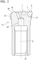
- FIG. 2 is a cross-sectional view illustrating a drilling tool according to an embodiment of the invention which has the drilling tip according to the embodiment attached thereon.
- the drilling tip according to this embodiment has a tip body 1, and this tip body 1 is provided with a body 2 which is made of a hard material such as a cemented carbide and a hard layer 3 which is coated on a surface of at least a tip portion (upper portion in FIG. 1 ) of the body 2 and has a higher hardness (Vickers hardness) than the body 2.
- a posterior end portion (lower portion in FIG. 1 ) has a cylindrical or disk shape with a tip central line C as a center, and a tip portion has a hemispherical shape having a center on the tip central line C with the same radius as that of the cylindrical or disk shape of the posterior end portion in this embodiment and is formed into a tapered shape in which the outer diameter from the tip central line C is gradually reduced toward a tip side. That is, the drilling tip according to this embodiment is a button tip.
- the hard layer 3 has a two-layer structure composed of an outermost layer 4 and an intermediate layer 5 which is interposed between the outermost layer 4 and the body 2.
- a drill bit as an embodiment of the drilling tool which has the drilling tip attached on the tip portion thereof has a bit body 11 made of steel or the like and has a substantially bottomed cylindrical shape with an axial line O as a center as illustrated in FIG. 2 .
- the bottomed portion of the bit body is a tip portion (upper portion in FIG. 2 ), and the drilling tip is attached on the tip portion.
- a female thread portion 12 is formed at the inner periphery of a posterior end portion (lower portion in FIG. 2 ) of the cylindrical shape, and a drill rod (not shown) connected to a drilling machine is screwed in the female thread portion 12.
- the drilling tip breaks bedrock, thereby forming a borehole.
- the tip portion of the bit body 11 has a slightly larger outer diameter than the posterior end portion.
- a plurality of discharge grooves 13 extending in parallel to the axial line O are formed at intervals in a circumferential direction. Crushed rubbish generated by breaking bedrock using the drilling tip is discharged to a posterior end side of the bit body 11 through the discharge grooves 13.
- a blow hole 14 is formed along the axial line O from a bottom surface of the female thread portion 12 of the bottomed bit body 11. This blow hole 14 is obliquely branched in the tip portion of the bit body 11 and opened to a tip surface of the bit body 11. A fluid such as compressed air supplied via the drill rod is ejected from the blow hole 14, and thus discharge of crushed rubbish is promoted.
- the tip surface of the bit body 11 is provided with a circular face surface 15 around an axial line O perpendicular to the axial line O on the inner peripheral side as a center and a frustconical gauge face 16 positioned at an outer periphery of the face surface 15 and extending toward the posterior end side as extending toward the outer periphery side.
- the blow hole 14 is opened to the face surface 15, and a tip of the discharge groove 13 is opened to the outer peripheral side of the frustconical gauge face 16.
- Each of the face surface 15 and the frustconical gauge face 16 has a plurality of fitting holes 17 having a circular cross section that are formed perpendicular to the face surface 15 and the frustconical gauge face 16 to avoid the opening portions of the blow hole 14 and the discharge groove 13.
- the drilling tip is attached in such a manner that it is fitted in by pressing, shrink fitting, or the like, or brazed to be fixed to, that is, buried in the fitting holes 17, in a state in which the posterior end portion of the tip body 1 is buried as illustrated in FIG. 2 .
- the tip portion of the tip body 1 having the hard layer 3 formed thereon protrudes from the face surface 15 and the frustconical gauge face 16 and breaks bedrock with the above-described striking force, impelling force, and rotating force.
- the outermost layer 4 is formed of a cubic boron nitride sintered material (hereinafter, also referred to as "cBN sintered material") in which the main binder phase is formed of ceramics.
- the cBN sintered material includes cubic boron nitride grains (hereinafter, also referred to as "cBN grains") of which the content is 70 to 95 vol% with respect to the whole cBN sintered material, and a binder phase binding the cBN grains to each other.
- a binder phase having a width of 1nm or greater and 30nm or less exists between neighboring cBN grains.
- This binder phase includes at least aluminum (Al), boron (B), and nitrogen (N), and a ratio (O/Al) of the oxygen (O) content to the Al content in the binder phase is 0.1 or less (atomic ratio calculated from an area ratio of the cross section).
- the lower limit value of the ratio of the O content to the Al content is 0.
- the above-described binder phase strongly binds the cBN grains to each other since it has a low oxide content.
- the cBN sintered material having the above-described binder phase the cBN grains are brought into contact with each other, and an unsintered portion which cannot sufficiently react with the binder phase is small. Therefore, such a cBN sintered material has a high hardness.
- the drilling tip can have a hardness comparable to a polycrystalline diamond sintered material, and thus the wear resistance of the drilling tip can be secured.
- the configuration of a binder phase other than the binder phase having a width of 1nm or greater and 30nm or less and existing between neighboring cBN grains among the binder phases formed in the cBN sintered material is not particularly limited, and preferably includes one or more selected from a nitride, a carbide, a carbonitride, and a boride of Ti, a nitride, a boride, and an oxide of Al, and solid solutions of two or more thereof; and inevitable impurities.
- the Vickers hardness of the outermost layer 4 is preferably 3,700 to 4,250. In a case where the Vickers hardness is less than 3,700, it is difficult to impart sufficient wear resistance to the outermost layer 4. In a case where the Vickers hardness is greater than 4,250, the outermost layer 4 is likely to fracture.
- the content of the cBN grains in the outermost layer 4 is 70 to 95 vol%, the above-described cross-sectional structure can be formed, and the Vickers hardness of the outermost layer 4 can be adjusted within the above-described range. In a case where the content of the cBN grains is less than 70 vol%, the amount of the cBN grains is small, and thus the Vickers hardness of the outermost layer 4 cannot be adjusted to 3,700 or greater. In addition, it is difficult to form a binder phase having a width of 1nm or greater and 30nm or less between the cBN grains.
- the amount of a compound containing Al, B, and N in the binder phase becomes relatively smaller than that of a binder phase component (for example, Ti or Ta compound or boride of Al) other than the above compound. Therefore, uniform sintering cannot be performed, and a structure exhibiting the above-described effects cannot be obtained. That is, in comparison to the binder phase containing Al, B, and N, the Ti compound or Al boride has a low adhesion strength to the cBN grains, and thus an interface between the Ti compound or Al boride and the cBN grains is likely to become a starting point of cracks. As a result, the fracture resistance is reduced.
- a binder phase component for example, Ti or Ta compound or boride of Al
- the content of the cBN grains is greater than 95 vol%, voids to be a starting point of cracks are likely to be formed in the sintered material, and thus the fracture resistance is reduced.
- the content of the cBN grains is preferably 70 to 92 vol%, and more preferably 75 to 90 vol%, but not limited thereto.
- the average grain size of the cBN grains is preferably 0.5 to 8.0 ⁇ m.
- high fracture resistance can be imparted to the outermost layer 4.
- propagation of cracks proceeding from the interface between the cBN grains and the binder phase or cracks proceeding through the cBN grains, occurring by a stress applied to the outermost layer 4 during drilling can be suppressed by the cBN grains dispersed in the cBN sintered material.
- the average grain size of the cBN grains is more preferably 0.5 to 3.0 ⁇ m, but not limited thereto.
- a binder phase having a width of 1nm or greater and 30nm or less and containing Al, B, and N, and in which a ratio O/A1 of the O content to the Al content is 0.1 or less, be observed in 60% or greater of the total number of visual fields observed.
- the fact that the content of such a binder phase is large means that there are many networks in which the neighboring cBN grains are strongly bound by the binder phase.
- the number of visual fields in which such a binder phase is observed is more preferably 80% or greater of the total number of visual fields, and even more preferably 100% (the binder phase is observed in all of the visual fields).
- a ratio (q/Q) of the number (q) of cBN grains with a binder phase, which has a width of 1nm or greater and 30nm or less and includes Al, B and N between the neighboring cBN grains, to the number (Q) of all of the cBN grains is 0.4 or greater.
- a ratio (n/N) of the number (n) of cBN grains with a binder phase, which has a width of 1nm or greater and 30nm or less, includes Al, B and N, and exists between the neighboring cBN grains, and in which a ratio O/Al of the O content to the Al content is 0.1 or less, to the number (N) of cBN grains with a binder phase, which has a width of 1nm or greater and 30nm or less, includes Al, B and N, and exists between the neighboring cBN grains, is 0.5 or greater.
- the fact that the ratio q/Q and the ratio n/N are high means that the cBN grains are strongly bound by the binder phase.
- the hardness of the outermost layer 4 can be improved.
- the upper limit of the value of the ratio q/Q is preferably 1, and the value of q/Q is more preferably 0.6 to 1.
- the value of the ratio n/N is preferably 0.6 to 1, and more preferably 0.8 to 1.
- the binder phase which exists between neighboring cBN grains has a width of 1nm or greater and 30nm or less, and contains Al, B, and N may exist in places between the neighboring cBN grains, or one binder phase may extend between the cBN grains (a cBN grain may be adjacent to another cBN grain via one binder phase described above).
- the average grain size of the cBN grains can be obtained as follows.
- a cross-sectional structure of the cBN sintered material is observed by a scanning electron microscope (SEM) to obtain a secondary electron image.
- SEM scanning electron microscope
- the secondary electron image has a size of 15 ⁇ m ⁇ 15 ⁇ m (5-time angle of the average grain size of the cBN grains before sintering).
- the secondary electron image is displayed in monochrome with 256 shades of gray ranging from 0 corresponding to black to 255 corresponding to white.
- a binarization process is performed such that the cBN grains are black.
- the pixel value of the cBN grains portions or the binder phase portions is obtained from an average within a region of approximately 0.5 ⁇ m ⁇ 0.5 ⁇ m. It is preferable that in the same image, average pixel values of at least 3 regions be obtained, and the obtained values be defined as contrast of the regions.
- the cBN grains and the binder phase are distinguished from each other.
- a separation process is performed for a portion thought to be cBN grains brought into contact with each other.
- cBN grains thought to be brought into contact with each other are separated using watershed as an image process operation. In this manner, portions corresponding to cBN grains are extracted by the image process from the image obtained by performing the binarization process on the secondary electron image.
- the portions (black portions) corresponding to the cBN grains extracted by the above-described process are subjected to grain analysis, and maximum lengths of the portions corresponding to the cBN grains are obtained, respectively.
- the obtained maximum lengths are defined as maximum lengths of the respective cBN grains, and the maximum lengths are defined as diameters of the respective cBN grains.
- Volumes of the respective cBN grains are calculated from the obtained diameters by assuming that the cBN grains are spheres. Based on the volumes of the respective cBN grains, a cumulative distribution of the grain sizes of the cBN grains is obtained.
- the sum of the volumes of the respective cBN grains and the volumes of cBN grains having a diameter which is not greater than the diameters of the above cBN grains is obtained as an integrated value.
- a graph having a vertical axis representing a volume percentage [%] which is a ratio of the integrated value of the respective cBN grains to the sum of the volumes of all of the cBN grains and a horizontal axis representing a diameter [ ⁇ m] of the respective cBN grains is drawn.
- a diameter (median diameter) in which the volume percentage is 50 vol% is defined as an average grain size of the cBN grains in one image.
- the average of the average grain sizes obtained by performing the above-described process on at least 3 secondary electron images is defined as an average grain size [ ⁇ m] of the cBN grains in the outermost layer 4.
- a length ( ⁇ m) per pixel is set using a value of a scale known in advance by SEM.
- a region having a diameter which is less than 0.02 ⁇ m is not calculated as a grain in order to remove noise.
- the content of the cBN grains can be adjusted by adjusting the mixing ratio between a cBN grain powder and a raw material powder for binder phase formation in the formation of the outermost layer 4.
- the content can be confirmed as follows. That is, an optional cross section of the outermost layer 4 is observed by SEM to obtain a secondary electron image. In the obtained secondary electron image, portions corresponding to cBN grains are extracted by the same image process as above. An area occupied by the cBN grains is calculated by image analysis, and a ratio of the cBN grains in one image is obtained.
- the average of the contents of the cBN grains obtained by processing at least 3 images is defined as a content of the cBN grains in the outermost layer 4.
- a square region in which one side has a length which is 5 times the average grain size of the cBN grains is preferably an observation region used in the image process.
- a visual field region of approximately 15 ⁇ m ⁇ 15 ⁇ m is preferable.
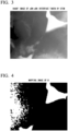
- FIG. 3 is a high angle annular dark field (HAADF) image (80,000 magnifications), taken by observing the interface between the cBN grains using the STEM.
- the thickness of the observation sample is preferably 3 nm to 70 nm.
- the thickness be smaller than 3 nm since the quantity of characteristic X-rays to be detected is reduced in elemental mapping, and thus a long period of time is taken for the measurement, and the sample is likely to be damaged. It is not preferable that the thickness be larger than 70 nm, since it becomes difficult to perform image analysis.
- the size of the observation image is increased from 150 nm (vertical) ⁇ 150 nm (horizontal) to approximately 500 nm (vertical) ⁇ 500 nm (horizontal), and the resolution is increased to 512 ⁇ 512 pixels or more.
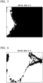
- elemental mapping images (see FIGS. 4 to 6 and 12 ) of B, N, Al, and O are obtained.
- These elemental mapping images are images obtained by conversion into a ratio (atm%) of the content of each element with respect to a total of the contents of the four elements in order to remove the background. Based on these images, whether a binder phase having a width of 1nm or greater and 30nm or less and containing Al, B, and N exists between neighboring cBN grains is confirmed in accordance with the following procedures (a) to (d), and a ratio of Al and a ratio of O in the binder phase is obtained.
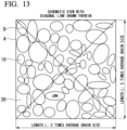
- the ratio (q/Q) of the number (q) of cBN grains with a binder phase, which has a width of 1nm or greater and 30nm or less and includes Al, B and N, between neighboring cBN grains, to the number (Q) of all of the cBN grains can be measured as follows. First, in an optional cross section of the outermost layer 4, a square region in which a length L of one side is 5 times the average grain size of cBN grains 10 is determined as one measurement visual field range A as illustrated in the schematic view of FIG. 13 . For example, in a case where the average grain size of the cBN grains is 1 ⁇ m, a square region of 5 ⁇ m ⁇ 5 ⁇ m is determined as one measurement visual field range.
- a diagonal line D is drawn from a vertex of the square measurement visual field range A, and the number Q 1 of cBN grains 10 overlapping the diagonal line D is counted.
- a binder phase 20 having a width of 1nm or greater and 30nm or less and containing Al, B, and N exists between each of the cBN grains 10 overlapping the diagonal line D and a cBN grain 10 neighboring thereto is specified by the above-described method.
- the number q 1 of cBN grains 10 specified as being grains with a binder phase 20, which has a width of 1nm or greater and 30nm or less and includes Al, B and N between the neighboring cBN grains, 10 is counted.
- q 1 /Q 1 is calculated using the number q 1 of cBN grains 10 and the number Q 1 of cBN grains 10 obtained. q 1 /Q 1 is calculated in at least 5 visual fields, and an average thereof is defined as the above-described ratio q/Q.
- the ratio (n/N) of the number (n) of cBN grains with a binder phase, which has a width of 1nm or greater and 30nm or less and includes Al, B, and N, and in which a ratio O/A of the O content to the Al content is 0.1 or less exists between the neighboring cBN grains, to the number (N) of cBN grains with a binder phase, which has a width of 1nm or greater and 30nm or less and includes Al, B and N between the neighboring cBN grains, can be measured as follows. First, in the schematic view of FIG.
- cBN grains 10 with a binder phase 20, which has a width of 1nm or greater and 30nm or less and includes Al, B and N between the cBN grains, 10 are specified among the cBN grains overlapping the diagonal line D, and the number N 1 of the above cBN grains is counted.
- cBN grains 10 in which the ratio O/Al of the O content to the Al content of a binder phase 20 having a width of 1nm or greater and 30nm or less and containing Al, B, and N is 0.1 or less are specified by the above-described method, and the number n 1 of the above cBN grains is counted.
- n 1 of cBN grains 10 and the number N 1 of cBN grains 10 obtained a value of n 1 /N 1 is calculated.
- n 1 /N 1 is calculated in at least 5 visual fields, and an average thereof is defined as the above-described ratio n/N.
- At least one intermediate layer 5 is provided between the outermost layer 4 and the body 2. Accordingly, it is possible to prevent the outermost layer 4 from being peeled. That is, in a case where an outermost layer 4 formed of the above-described cBN sintered material is directly formed on the body 2, a stress remains after sintering due to a difference in the shrinkage ratio between the outermost layer 4 and the body 2 made of a hard material such as a cemented carbide, and cracks occur between an interface between the body 2 and the outermost layer 4. In this embodiment, since the intermediate layer 5 is provided between the outermost layer 4 and the body 2, the intermediate layer 5 functions as a stress relaxation layer. As a result, it is possible to suppress the occurrence of cracks, and it is possible to prevent the outermost layer 4 from being peeled.
- the configuration of the intermediate layer 5 is not particularly limited as long as the intermediate layer has a less hardness (Vickers hardness) which is less than the outermost layer 4 and greater than the body 2.
- the intermediate layer 5 may be a cBN sintered material obtained by sintering with a catalytic metal containing Al and at least one of Co, Ni, Mn, and Fe.
- a metallic additive containing at least one of W, Mo, Cr, V, Zr, and Hf may be added to the metallic catalyst.
- the intermediate layer 5 may be formed of a polycrystalline diamond sintered material including diamond, cobalt, and tungsten carbide.
- the intermediate layer 5 preferably contains 30 to 70 vol% of cBN grains or diamond grains.
- the intermediate layer 5 has a less hardness than the body 2.
- the intermediate layer 5 has the same hardness as the outermost layer 4. Accordingly, the content of the cBN grains or diamond grains in the intermediate layer 5 is preferably 30 to 70 vol% to allow the intermediate layer to function as a stress relaxation layer.
- the intermediate layer 5 has a single layer structure.
- the intermediate layer 5 may have a multi-layer structure.
- the thickness of the outermost layer 4 on the tip central line C is preferably 0.3 mm to 1.5 mm. In a case where the thickness of the outermost layer 4 is 0.3 mm or smaller, there is a concern that the drilling tip may be rapidly abraded and its life may thus be reduced. In a case where the thickness of the outermost layer 4 is 1.5 mm or larger, there is a concern that cracks may be likely to occur due to a residual stress during sintering, and thus unexpected fractures may be caused during drilling.
- the thickness of the outermost layer 4 is more preferably 0.4 mm to 1.3 mm.
- the total thickness of the intermediate layer 5 on the tip central line C is preferably 0.2 mm to 1.0 mm.
- the thickness of the intermediate layer 5 is 0.2 mm or smaller, there is a concern that it may be difficult to form a uniform layer, and thus it may be difficult to absorb a residual stress during sintering, and the intermediate layer may not function to relax the stress of the tip.
- the thickness of the intermediate layer 5 is 1.0 mm or larger, the total thickness of the hard layer 3 (outermost layer 4 and intermediate layer 5) is increased, and thus there is a concern that cracks may be likely to occur due to a residual stress during sintering, and thus unexpected fractures may be caused during drilling.
- the total thickness of the intermediate layer 5 is more preferably 0.3 mm to 0.8 mm.
- the method of manufacturing a drilling tip includes a step of performing a pretreatment on surfaces of cBN grains to form an AlN film, a step of obtaining a mixed powder of the pretreated cBN grains and a raw material powder for a binder phase of the outermost layer 4, and a step of sintering the mixed powder, a raw material powder for the intermediate layer 5, and the body 2.
- the pretreatment for surfaces of cBN grains is performed as follows to obtain cBN grains having a high surface cleanliness.
- a film forming method for example, an atomic layer deposition (ALD) method can be used.
- the ALD method is a type of CVD method, and is a method of reacting a base material in a vacuum chamber with molecules of a raw material compound for each layer to repeatedly perform purge by Ar or nitrogen, thereby forming a film.
- a film forming method for example, an atomic layer deposition (ALD) method can be used.
- the ALD method is a type of CVD method, and is a method of reacting a base material in a vacuum chamber with molecules of a raw material compound for each layer to repeatedly perform purge by Ar or nitrogen, thereby forming a film.
- cBN grains as a base material are charged into a fluidized bed furnace, and the temperature in the furnace is increased
- a cycle of an Ar+Al(CH 3 ) 3 gas inflow step, an Ar gas purge step, an Ar+NH 3 gas inflow step, and an Ar gas purge step is repeatedly performed until a desired AlN film thickness is obtained.
- a desired AlN film thickness For example, an AlN film having a film thickness of approximately 5 nm can be coated on the surfaces of the cBN grains by film formation for 30 minutes.
- the cBN grains coated with the AlN film are heated at approximately 1,000°C under vacuum. Accordingly, impurity elements such as oxygen of the surfaces of the cBN grains are diffused and captured in the AlN film. Finally, by mixing the cBN grains through ball-mill mixing, the AlN film capturing the impurity elements is peeled from the surfaces of the cBN grains.
- cBN grains having a high surface cleanliness, in which impurity components such as oxygen are removed from surfaces are obtained.
- the pretreatment for surfaces of cBN grains is not limited to the above-described treatment, and any method can be used as long as it is a method for removing impurity components of the surfaces of the cBN grains.
- the pretreated cBN grains are mixed with a raw material powder for a binder phase of the outermost layer 4 to obtain a predetermined composition, and a mixed powder is obtained.
- a raw material powder for a binder phase of the outermost layer 4 a TiN powder, an Al powder, a TiAl 3 powder, and an Al 2 O 3 powder can be used.
- the obtained mixed powder, a raw material powder for the intermediate layer 5, and the body 2 are subjected to ultra-high-pressure and high-temperature sintering.
- the tip body 1 of the drilling tip according to this embodiment can be manufactured.
- the outermost layer 4 having the above-described configuration can be formed by using, as cBN grains of the outermost layer 4, cBN grains of which the surface cleanliness has been increased by the pretreatment, and by subjecting the cBN grains to ultra-high-pressure and high-temperature sintering.
- the sintering is performed at a temperature of 1,500°C or higher with a pressure of 5.0 GPa or greater in a stable region of diamond and cubic boron nitride. Accordingly, the outermost layer 4 and the intermediate layer 5 can be simultaneously formed on the body 2.
- the sintering pressure is more preferably 5.5 GPa to 8.0 GPa, and the sintering temperature is more preferably 1,600°C to 1,800°C.
- the above step is performed to prevent oxidation of the raw material powder, and specifically, the raw material powder or molded body is preferably handled under a non-oxidizing protective atmosphere.
- the drilling tip, the drilling tool, and the method of manufacturing a drilling tip according to the embodiment of the disclosure have been described.
- a case where the disclosure is applied to a button-type drilling tip in which the tip portion of the tip body 1 has a hemispherical shape has been described as above.
- the disclosure can also be applied to a so-called ballistic-type drilling tip in which a tip portion of a tip body 1 has a shell shape, or a so-called spike-type drilling tip in which a tip portion on a posterior end side has a conical surface shape of which the diameter is reduced toward a tip side, and a tip thereof has a spherical shape with a radius smaller than that of a cylindrical posterior end portion of a tip body 1.
- the drilling tip according to the disclosure can also be applied to a pick attached to an outer periphery of a rotation drum of a drum drilling machine for use in opencast mining or longwall mining.
- cBN grains having a median diameter (D50) shown in Table 1 were used as a base material, and through an ALD method, an AlN film having an average film thickness shown in Table 1 was coated thereon. Specifically, first, cBN grains were charged into a furnace, and the temperature in the furnace was increased to 350°C. Next, using a film forming gas which was an Al(CH 3 ) 3 gas as an Al precursor and a reaction gas which was a NH 3 gas, a cycle of the following (1) to (4) was repeated until an AlN film having a target film thickness was formed.
- a film forming gas which was an Al(CH 3 ) 3 gas as an Al precursor
- a reaction gas which was a NH 3 gas a cycle of the following (1) to (4) was repeated until an AlN film having a target film thickness was formed.
- the cBN grains were observed by SEM, and thus an AlN film having an average film thickness shown in Table 1 was confirmed to be coated on surfaces of the cBN grains.
- the cBN grains coated with the AlN film were heat-treated for 30 minutes at approximately 1,000°C under vacuum to diffuse impurity elements such as oxygen of the surfaces of the cBN grains in the AlN film.
- the heat-treated cBN grains were mixed through ball-mill mixing using a tungsten carbide container and balls, and the AlN film was peeled from the surfaces of the cBN grains.
- a TiN powder, a TiC powder, an Al powder, a TiAl 3 powder, and a WC powder having an average grain size within a range of 0.3 to 0.9 ⁇ m were prepared as raw material powders for a binder phase. Two or more selected from the above raw material powders and the cBN grain powder pretreated as described above were blended such that the content of the cBN grain powder was 70 to 95 vol% in a case where the total amount of the powders was 100 vol%. Then, the mixture was subjected to wet blending and dried. Thereafter, the mixture was press-molded into dimensions of 50 mm in diameter and 1.5 mm in thickness at a molding pressure of 1 MPa using a hydraulic press to obtain a molded body.
- cBN sintered materials 1 to 17 of a drilling tip of the present disclosure (hereinafter referred to as "cBN sintered materials 1 to 17 of the present disclosure") shown in Table 2 were prepared.
- comparative cBN sintered materials 1 to 10 were prepared as follows. First, cBN grains a to i having a median diameter (D50) shown in Table 4 were prepared. The cBN grains a, b, and e to i were not pretreated in the same manner as in the cases of the cBN sintered materials 1 to 17 of the present disclosure. The cBN grains c and d were pretreated in the same manner as in the cases of the cBN sintered materials 1 to 17 of the present disclosure, so that an AlN film having an average film thickness shown in Table 4 was formed on surfaces of the cBN grains, and then peeled therefrom.
- D50 median diameter
- a binder phase structure other than cBN was confirmed by X-ray diffraction (XRD).
- XRD X-ray diffraction
- the average grain size ( ⁇ m) of the cBN grains and the content (vol%) of the cBN grains were measured by the above-described methods, respectively.
- the observation region used in the image process had a size of 15 ⁇ m ⁇ 15 ⁇ m. The results are shown in Tables 2 and 5.
- a Vickers hardness (Hv) was measured at a load of 5 kg. The average of the measured values is shown in Tables 2 and 5 as an average Vickers hardness. Each value was rounded off to the nearest 10.
- a graph obtained by plotting the relationship between the cBN content C (vol%) and the Vickers hardness H (Hv) of Tables 2 and 5 is shown in FIG. 14 .
- the presence or absence of a binder phase which had a width of 1nm or greater and 30nm or less and contained Al, B, and N, and in which the ratio O/Al of the O content to the Al content was 0.1 or less between neighboring cubic boron nitride grains was observed in 10 visual fields.
- the number of visual fields in which such a binder phase can be observed is shown in Tables 3 and 6 as the number of observation visual fields.
- the number Q 1 of cBN grains, the number q 1 (N 1 ) of cBN grains with a binder phase, which has a width of 1nm or greater and 30nm or less and includes Al, B and N, between neighboring cBN grains, and the number n 1 of cBN grains in which the ratio O/Al of the O content to the Al content in the binder phase was 0.1 or less were obtained as described above.
- a ratio (q/Q) of cBN grains with a binder phase which has a width of 1nm or greater and 30nm or less and includes Al, B and N, between neighboring cBN grains, and a ratio (n/N) of cBN grains in which ha binder phase which had a width of 1nm or greater and 30nm or less and contained Al, B, and N, and in which the ratio O/Al of the O content to the Al content was 0.1 or less existed between neighboring cBN grains were obtained.
- the results are shown in Tables 3 and 6.
- the cBN sintered materials 1 to 17 of the present disclosure were also confirmed to have a Vickers hardness (Hv) of greater than 3,700.
- the ratio (O/Al) of the O content to the Al content was 0.1 or less on average, and the amount of oxides was small. However, since the cBN content was less than 70 vol% or greater than 95 vol%, the Vickers hardness (Hv) was low.
- the comparative cBN sintered material 6 had a lower Vickers hardness (Hv) than the cBN sintered material 8 of the present disclosure having the same cBN grain content. In all other comparative cBN sintered materials 1, 2, 5, and 7 to 10, the ratio (O/Al) of the O content to the Al content was greater than 0.1, and thus the Vickers hardness (Hv) was low.
- the Vickers hardness of all of the comparative cBN sintered materials 1 to 10 was positioned below the curve. From these facts, it was found that the Vickers hardness of the cBN sintered materials of the present disclosure was higher than that of the comparative cBN sintered materials even in a case where these had the same cBN grain content.
- the curve represents the relationship between the cBN grain content and the Vickers hardness of the cBN sintered materials obtained by experiences.
- An unpretreated cBN powder having a grain size of 9.6 ⁇ m, a W powder having a grain size of 4 ⁇ m, an Al powder having a grain size of 0.9 ⁇ m, and a Co powder having a grain size of 3 ⁇ m were blended as shown in Table 8. Then, the mixture was subjected to wet blending and dried. Accordingly, raw material powders for an intermediate layer of Examples 1 to 3 were obtained. In addition, diamond grains having a grain size of 8 ⁇ m, a Co powder having a grain size of 3.7 ⁇ m, and a WC powder having a grain size of 2.1 ⁇ m were blended such that the content of the diamond grains was as shown in Table 8 in a case where the total amount of the powders was 100 vol%. Then, the mixture was subjected to wet blending and dried. Accordingly, a raw material powder for an intermediate layer of Example 4 was obtained.
- the raw material powders for an outermost layer and the raw material powders for an intermediate layer of Examples 1 to 4 were integrally sintered together with a body made of a cemented carbide containing 94 wt% of WC and 6 wt% of Co under conditions of a sintering pressure of 6.0 GPa, a sintering temperature of 1,600°C, and a sintering time of 20 minutes. Accordingly, button tips (drilling tips) according to Examples 1 to 4, having a radius of 5.5 mm and a length of 16 mm in a tip central line direction, were manufactured. The radius of a hemispherical tip portion of a tip body was 5.75 mm.
- the layer thicknesses of the outermost layer and the intermediate layer in the tip central line direction were as shown in Tables 7 and 8.
- a button tip (Comparative Example 1) in which hard grains of an outermost layer were not cBN grains, but were diamond grains, a button tip (Comparative Example 2) in which a metallic catalyst was used as a binder phase of an outermost layer, a button tip (Comparative Example 3) in which the content of cBN grains contained in an outermost layer was less than 70 vol%, a button tip (Comparative Example 4) in which no intermediate layer was provided, and a button tip (Comparative Example 5) in which the content of cBN grains contained in an outermost layer was greater than 95 vol% were manufactured.
- the button tips of Comparative Examples 1 to 5 all had the same dimensions as Examples 1 to 4 of present disclosure.
- Unpretreated hard grains (diamond grains or cBN grains) were used in the outermost layers of the button tips of Comparative Examples 1 and 2. Specifically, regarding the button tip of Comparative Example 1, diamond grains having a grain size of 8 ⁇ m, a Co powder having a grain size of 3 ⁇ m, and a WC powder having a grain size of 2.7 ⁇ m were blended such that the content of the diamond grains was as shown in Table 7 in a case where the total amount of the powders was 100 vol%. Then, the mixture was subjected to wet blending and dried. In this manner, a raw material powder for an outermost layer was obtained.
- This raw material powder for an outermost layer and the same raw material powder for an intermediate layer as used in Examples 1 to 4 of present disclosure were integrally sintered together with a body made of the same cemented carbide as used in Examples 1 to 4 of present disclosure under conditions of a sintering pressure of 5.4 GPa, a sintering temperature of 1,450°C, and a sintering time of 5 minutes.
- an unpretreated cBN grain powder having a grain size of 4.1 ⁇ m, a W powder having a grain size of 1.5 ⁇ m, an Al powder having a grain size of 0.3 ⁇ m, and a Co powder having a grain size of 3 ⁇ m were blended such that the content of the cBN grain powder was as shown in Table 7 in a case where the total amount of the powders was 100 vol%. Then, the mixture was subjected to wet blending and dried. In this manner, a raw material powder for an outermost layer was obtained.
- This raw material powder for an outermost layer and the same raw material powder for an intermediate layer as used in Examples 1 to 4 of present disclosure were integrally sintered together with a body made of the same cemented carbide as used in Examples 1 to 4 of present disclosure under conditions of a sintering pressure of 5.0 GPa, a sintering temperature of 1,600°C, and a sintering time of 30 minutes.
- the button tips of Comparative Examples 3 and 5 were prepared in the same manner as in Examples 1 to 4 of present disclosure.
- the button tip of Comparative Example 4 was prepared in the same manner as in Examples 1 to 4 of present disclosure, except that no intermediate layer was provided.
- the layer thicknesses of the outermost layer and the intermediate layer in a tip central line direction of Comparative Examples 1 to 5 were as shown in Tables 7 and 8.
- the drilling length was 124 m, and the drilling tip life was reached due to fractures.
- the drilling length did not reach 100 m, and the drilling tip life was reached due to fractures.
- the drilling tip life was reached due to normal wear, but the drilling length did not reach 100 m.
- Comparative Example 4 In Comparative Example 4 in which no intermediate layer was provided, cracks occurred during sintering, and thus it was not possible to perform the drilling using the drilling tip of Comparative Example 4.
- Comparative Example 5 In Comparative Example 5 in which the content of the cBN grains of the outermost layer was large, cracks occurred during sintering due to ununiformity during sintering in the outermost layer, and thus it was not possible to perform the drilling using the drilling tip of Comparative Example 5.
- Example 1 to 4 of present disclosure attached thereon, respectively, 400 m or more of drilling was possible even in Example 3 of present disclosure in which the drilling length was the shortest.
- a drilling tip according to the disclosure has a hardness comparable to a polycrystalline diamond sintered material, and thus secures wear resistance and can be used in Fe or Ni mines or under high-temperature drilling conditions. Therefore, the drilling tip is suitable for bits for mine drilling, bits for construction drilling, bits for oil and gas (O & G) drilling, and picks of drum drilling machines for use in opencast mining or longwall mining.
- bits for mine drilling bits for construction drilling
- bits for oil and gas (O & G) drilling bits for oil and gas (O & G) drilling
- picks of drum drilling machines for use in opencast mining or longwall mining.
Landscapes
- Chemical & Material Sciences (AREA)
- Engineering & Computer Science (AREA)
- Mechanical Engineering (AREA)
- Materials Engineering (AREA)
- Mining & Mineral Resources (AREA)
- Organic Chemistry (AREA)
- Life Sciences & Earth Sciences (AREA)
- Geology (AREA)
- Ceramic Engineering (AREA)
- Metallurgy (AREA)
- General Life Sciences & Earth Sciences (AREA)
- Geochemistry & Mineralogy (AREA)
- General Chemical & Material Sciences (AREA)
- Chemical Kinetics & Catalysis (AREA)
- Structural Engineering (AREA)
- Physics & Mathematics (AREA)
- Environmental & Geological Engineering (AREA)
- Fluid Mechanics (AREA)
- Manufacturing & Machinery (AREA)
- Crystallography & Structural Chemistry (AREA)
- Composite Materials (AREA)
- Inorganic Chemistry (AREA)
- Cutting Tools, Boring Holders, And Turrets (AREA)
- Earth Drilling (AREA)
- Powder Metallurgy (AREA)
Claims (6)
- Une pointe de forage qui est fixée à une partie de la pointe d'un outil de forage pour effectuer le forage, la pointe de forage comprenant:un corps de pointe (1) pourvu d'une partie d'extrémité postérieure enfouie dans le corps de l'outil de forage, et d'une partie de pointe faisant saillie à partir d'une surface de l'outil de forage et étant effilée vers un côté de pointe du corps de pointe (1); etune couche dure (3) formée sur une surface de la partie de la pointe du corps de la pointe (1),la couche dure (3) étant constituée d'une couche externe (4) et d'une couche intermédiaire (5) interposée entre la couche externe (4) et le corps de la pointe (1),la couche externe (4) étant un matériau fritté à base de nitrure de bore cubique contenant de 70 à 95 % de grains de nitrure de bore cubique (10) et une phase liante (20),lorsqu'on observe la structure transversale de la couche externe (4), une phase liante (20) d'une largeur de 1 nm ou plus et de 30 nm ou moins, contenant de l'Al, du B et du N, et dans laquelle le rapport atomique entre la teneur en O et la teneur en Al est de 0,1 ou moins, existe entre les grains cubiques de nitrure de bore voisins (10),lorsqu'on observe la structure en coupe de la couche extérieure (4), un rapport de : un nombre de grains cubiques de nitrure de bore (10) dont la phase liante (20) a une largeur de 1 nm ou plus et de 30 nm ou moins, et contenant Al, B et N entre des grains cubiques de nitrure de bore voisins (10) : par rapport à un nombre total de grains cubiques de nitrure de bore (10), est supérieur ou égal à 0,4, etun rapport entre : un nombre de grains cubiques de nitrure de bore (10) dont la phase liante (20) a une largeur de 1 nm ou plus et de 30 nm ou moins, contenant Al, B et N, et dont le rapport atomique entre la teneur en O et la teneur en Al est de 0,1 ou moins entre les grains de nitrure de bore cubiques voisins (10) : au nombre de grains de nitrure de bore cubiques (10) qui ont la phase liante (20) ayant une largeur de 1 nm ou plus et de 30 nm ou moins et contenant Al, B et N entre les grains de nitrure de bore cubiques voisins (10), est de 0,5 ou plus.
- Pointe de forage selon la revendication 1,
dans laquelle la couche extérieure (4) a une dureté Vickers comprise entre 3 700 HV et 4 250 HV. - Pointe de forage selon la revendication 1 ou 2,
dans lequel les grains de nitrure de bore cubique (10) ont une taille moyenne de 0,5 à 8,0 mµ, la taille moyenne des grains étant déterminée conformément à la description. - Pointe de forage selon l'une des revendications 1 à 3,
dans laquelle la couche intermédiaire (5) contient de 30 à 70 % de grains de nitrure de bore cubique (10) ou de grains de diamant. - Outil de forage comprenantun corps d'outil; etla pointe de forage selon l'une des revendications 1 à 4 qui est fixé sur une partie de l'embout du corps de l'outil.
- Méthode de fabrication de la pointe de forage selon l'une des revendications 1 à 4, comprenant les étapes suivantes:prétraitement des surfaces des grains de nitrure de bore cubique (10) pour former un film AIN;obtenir une poudre mixte en mélangeant une poudre de matière première pour une phase de liant (20) de la couche extérieure (4) et les grains de nitrure de bore cubique prétraités (10); etfrittage de la poudre mélangée, d'une poudre de matière première pour la couche intermédiaire (5) et du corps de la pointe (1) à une pression de 5,0 GPa ou plus et à une température de 1 500° C ou plus.
Applications Claiming Priority (2)
| Application Number | Priority Date | Filing Date | Title |
|---|---|---|---|
| JP2016084176 | 2016-04-20 | ||
| PCT/JP2017/015749 WO2017183659A1 (fr) | 2016-04-20 | 2017-04-19 | Puce d'excavation, outil d'excavation et procédé de fabrication de puce d'excavation |
Publications (3)
| Publication Number | Publication Date |
|---|---|
| EP3447233A1 EP3447233A1 (fr) | 2019-02-27 |
| EP3447233A4 EP3447233A4 (fr) | 2019-11-20 |
| EP3447233B1 true EP3447233B1 (fr) | 2025-06-04 |
Family
ID=60116846
Family Applications (1)
| Application Number | Title | Priority Date | Filing Date |
|---|---|---|---|
| EP17785996.4A Active EP3447233B1 (fr) | 2016-04-20 | 2017-04-19 | Pointe de forage, outil de forage et méthode de fabrication de ladite pointe de forage |
Country Status (8)
| Country | Link |
|---|---|
| US (1) | US10900293B2 (fr) |
| EP (1) | EP3447233B1 (fr) |
| JP (1) | JP6853439B2 (fr) |
| KR (1) | KR102423112B1 (fr) |
| CN (1) | CN108699893B (fr) |
| AU (1) | AU2017254220B2 (fr) |
| CA (1) | CA3021570C (fr) |
| WO (1) | WO2017183659A1 (fr) |
Families Citing this family (2)
| Publication number | Priority date | Publication date | Assignee | Title |
|---|---|---|---|---|
| GB201720027D0 (en) * | 2017-12-01 | 2018-01-17 | Element Six (Uk) Ltd | Pick tool for road milling or mining |
| IT201900020168A1 (it) * | 2019-10-31 | 2021-05-01 | Silca Spa | Metodo per definire l’usura della fresa in una macchina duplicatrice di chiavi. |
Citations (1)
| Publication number | Priority date | Publication date | Assignee | Title |
|---|---|---|---|---|
| US20060166615A1 (en) * | 2002-01-30 | 2006-07-27 | Klaus Tank | Composite abrasive compact |
Family Cites Families (21)
| Publication number | Priority date | Publication date | Assignee | Title |
|---|---|---|---|---|
| US4694918A (en) | 1985-04-29 | 1987-09-22 | Smith International, Inc. | Rock bit with diamond tip inserts |
| US4811801A (en) | 1988-03-16 | 1989-03-14 | Smith International, Inc. | Rock bits and inserts therefor |
| US5011514A (en) * | 1988-07-29 | 1991-04-30 | Norton Company | Cemented and cemented/sintered superabrasive polycrystalline bodies and methods of manufacture thereof |
| JP2777017B2 (ja) * | 1992-06-30 | 1998-07-16 | 京セラ株式会社 | 立方晶窒化硼素質焼結体およびその製造方法 |
| US5837071A (en) | 1993-11-03 | 1998-11-17 | Sandvik Ab | Diamond coated cutting tool insert and method of making same |
| JPH08197307A (ja) | 1995-01-26 | 1996-08-06 | Mitsubishi Materials Corp | 高強度および高靭性を有する立方晶窒化ほう素基超高圧焼結材料製切削工具 |
| KR100263594B1 (ko) * | 1996-10-31 | 2000-08-01 | 오카야마 노리오 | 고경도 고인성 소결체 |
| JP3648205B2 (ja) | 2001-03-23 | 2005-05-18 | 独立行政法人石油天然ガス・金属鉱物資源機構 | 石油掘削用トリコンビットのインサートチップおよびその製造方法ならびに石油掘削用トリコンビット |
| JP2002319173A (ja) * | 2001-04-19 | 2002-10-31 | Matsushita Electric Ind Co Ltd | 光ヘッド装置 |
| JP2004026555A (ja) | 2002-06-25 | 2004-01-29 | Toshiba Tungaloy Co Ltd | 立方晶窒化ホウ素含有焼結体およびその製造方法 |
| EP2053198A1 (fr) | 2007-10-22 | 2009-04-29 | Element Six (Production) (Pty) Ltd. | Corps à pointe |
| JP5125646B2 (ja) * | 2008-03-19 | 2013-01-23 | 株式会社タンガロイ | 立方晶窒化硼素焼結体工具 |
| JP5182582B2 (ja) | 2008-12-09 | 2013-04-17 | 三菱マテリアル株式会社 | 立方晶窒化ホウ素の合成方法および立方晶窒化ホウ素焼結体の製造方法 |
| GB201002375D0 (en) * | 2010-02-12 | 2010-03-31 | Element Six Production Pty Ltd | A superhard tip, method for making same and tool comprising same |
| JP2011212832A (ja) * | 2010-03-19 | 2011-10-27 | Mitsubishi Materials Corp | 立方晶窒化ほう素基超高圧焼結材料製切削工具 |
| JP5126702B1 (ja) | 2011-09-12 | 2013-01-23 | 三菱マテリアル株式会社 | 立方晶窒化ほう素基焼結材料製切削工具 |
| JP5305056B1 (ja) | 2012-05-16 | 2013-10-02 | 三菱マテリアル株式会社 | 立方晶窒化ほう素基焼結体製切削工具 |
| JP5988164B2 (ja) * | 2013-01-31 | 2016-09-07 | 三菱マテリアル株式会社 | 立方晶窒化ほう素基焼結材料製切削工具 |
| JP6095162B2 (ja) * | 2013-03-29 | 2017-03-15 | 住友電工ハードメタル株式会社 | 立方晶窒化ホウ素焼結体 |
| KR102053198B1 (ko) | 2013-05-23 | 2019-12-06 | 엘지전자 주식회사 | 이동 단말기 |
| JP6343888B2 (ja) | 2013-08-27 | 2018-06-20 | 三菱マテリアル株式会社 | 耐欠損性にすぐれた立方晶窒化硼素焼結体切削工具 |
-
2017
- 2017-04-19 CA CA3021570A patent/CA3021570C/fr active Active
- 2017-04-19 CN CN201780011117.1A patent/CN108699893B/zh active Active
- 2017-04-19 JP JP2018513197A patent/JP6853439B2/ja active Active
- 2017-04-19 KR KR1020187025098A patent/KR102423112B1/ko active Active
- 2017-04-19 AU AU2017254220A patent/AU2017254220B2/en active Active
- 2017-04-19 US US16/094,774 patent/US10900293B2/en active Active
- 2017-04-19 EP EP17785996.4A patent/EP3447233B1/fr active Active
- 2017-04-19 WO PCT/JP2017/015749 patent/WO2017183659A1/fr not_active Ceased
Patent Citations (1)
| Publication number | Priority date | Publication date | Assignee | Title |
|---|---|---|---|---|
| US20060166615A1 (en) * | 2002-01-30 | 2006-07-27 | Klaus Tank | Composite abrasive compact |
Also Published As
| Publication number | Publication date |
|---|---|
| CN108699893B (zh) | 2020-06-23 |
| AU2017254220A1 (en) | 2018-11-22 |
| KR20180132046A (ko) | 2018-12-11 |
| US10900293B2 (en) | 2021-01-26 |
| CA3021570C (fr) | 2023-11-21 |
| US20190119988A1 (en) | 2019-04-25 |
| EP3447233A4 (fr) | 2019-11-20 |
| JP6853439B2 (ja) | 2021-03-31 |
| CN108699893A (zh) | 2018-10-23 |
| CA3021570A1 (fr) | 2017-10-26 |
| EP3447233A1 (fr) | 2019-02-27 |
| JPWO2017183659A1 (ja) | 2019-02-28 |
| KR102423112B1 (ko) | 2022-07-19 |
| WO2017183659A1 (fr) | 2017-10-26 |
| AU2017254220B2 (en) | 2021-12-23 |
Similar Documents
| Publication | Publication Date | Title |
|---|---|---|
| JP6881200B2 (ja) | 掘削チップ、掘削工具、および掘削チップの製造方法 | |
| EP3075476B1 (fr) | Outil de coupe à base de carbure cémenté revêtu de diamant | |
| EP3225608B1 (fr) | Matière fritté à base de nitrure de bore cubique et outil coupant constitué d'une matière fritté à base de nitrure de bore cubique | |
| US20220371962A1 (en) | Superhard constructions and methods of making same | |
| EP3447233B1 (fr) | Pointe de forage, outil de forage et méthode de fabrication de ladite pointe de forage | |
| WO2018122307A1 (fr) | Constructions super-dures et leurs procédés de fabrication | |
| WO2021182463A1 (fr) | Matériau composite dur | |
| WO2022210771A1 (fr) | Embout d'excavation, et outil d'excavation | |
| EP3936264A1 (fr) | Pièce frittée de nitrure de bore cubique et outil de coupe | |
| CN106164017B (zh) | 复合烧结体 | |
| JP6731185B2 (ja) | 立方晶窒化ほう素基焼結体および立方晶窒化ほう素基焼結体製切削工具 | |
| US20200269321A1 (en) | Superhard constructions & methods of making same | |
| US11383305B2 (en) | cBN sintered compact and cutting tool | |
| JP6933017B2 (ja) | 立方晶窒化ほう素基焼結体および切削工具 | |
| US11565317B2 (en) | Superhard constructions and methods of making same | |
| US12415761B2 (en) | Superhard constructions and methods of making same | |
| WO2022210760A1 (fr) | Embout d'excavation, et outil d'excavation | |
| JP2022142894A (ja) | cBN焼結体 |
Legal Events
| Date | Code | Title | Description |
|---|---|---|---|
| STAA | Information on the status of an ep patent application or granted ep patent |
Free format text: STATUS: THE INTERNATIONAL PUBLICATION HAS BEEN MADE |
|
| PUAI | Public reference made under article 153(3) epc to a published international application that has entered the european phase |
Free format text: ORIGINAL CODE: 0009012 |
|
| STAA | Information on the status of an ep patent application or granted ep patent |
Free format text: STATUS: REQUEST FOR EXAMINATION WAS MADE |
|
| 17P | Request for examination filed |
Effective date: 20181029 |
|
| AK | Designated contracting states |
Kind code of ref document: A1 Designated state(s): AL AT BE BG CH CY CZ DE DK EE ES FI FR GB GR HR HU IE IS IT LI LT LU LV MC MK MT NL NO PL PT RO RS SE SI SK SM TR |
|
| AX | Request for extension of the european patent |
Extension state: BA ME |
|
| DAV | Request for validation of the european patent (deleted) | ||
| DAX | Request for extension of the european patent (deleted) | ||
| RAP1 | Party data changed (applicant data changed or rights of an application transferred) |
Owner name: MITSUBISHI MATERIALS CORPORATION |
|
| A4 | Supplementary search report drawn up and despatched |
Effective date: 20191021 |
|
| RIC1 | Information provided on ipc code assigned before grant |
Ipc: B22F 7/00 20060101ALI20191015BHEP Ipc: C22C 26/00 20060101ALI20191015BHEP Ipc: E21C 35/183 20060101ALI20191015BHEP Ipc: E21B 10/46 20060101AFI20191015BHEP Ipc: C04B 41/89 20060101ALI20191015BHEP Ipc: C23C 16/455 20060101ALI20191015BHEP Ipc: C04B 35/58 20060101ALI20191015BHEP |
|
| STAA | Information on the status of an ep patent application or granted ep patent |
Free format text: STATUS: EXAMINATION IS IN PROGRESS |
|
| 17Q | First examination report despatched |
Effective date: 20210608 |
|
| RIC1 | Information provided on ipc code assigned before grant |
Ipc: C23C 16/56 20060101ALI20230926BHEP Ipc: C23C 16/34 20060101ALI20230926BHEP Ipc: C23C 16/01 20060101ALI20230926BHEP Ipc: C23C 16/455 20060101ALI20230926BHEP Ipc: C22C 26/00 20060101ALI20230926BHEP Ipc: E21C 35/183 20060101ALI20230926BHEP Ipc: C04B 41/89 20060101ALI20230926BHEP Ipc: C04B 35/58 20060101ALI20230926BHEP Ipc: E21B 10/46 20060101AFI20230926BHEP |
|
| GRAP | Despatch of communication of intention to grant a patent |
Free format text: ORIGINAL CODE: EPIDOSNIGR1 |
|
| STAA | Information on the status of an ep patent application or granted ep patent |
Free format text: STATUS: GRANT OF PATENT IS INTENDED |
|
| RIC1 | Information provided on ipc code assigned before grant |
Ipc: E21B 10/567 20060101ALI20241210BHEP Ipc: C23C 16/56 20060101ALI20241210BHEP Ipc: C23C 16/34 20060101ALI20241210BHEP Ipc: C23C 16/01 20060101ALI20241210BHEP Ipc: C23C 16/455 20060101ALI20241210BHEP Ipc: C22C 26/00 20060101ALI20241210BHEP Ipc: E21C 35/183 20060101ALI20241210BHEP Ipc: C04B 41/89 20060101ALI20241210BHEP Ipc: C04B 35/58 20060101ALI20241210BHEP Ipc: E21B 10/46 20060101AFI20241210BHEP |
|
| INTG | Intention to grant announced |
Effective date: 20250102 |
|
| GRAS | Grant fee paid |
Free format text: ORIGINAL CODE: EPIDOSNIGR3 |
|
| GRAA | (expected) grant |
Free format text: ORIGINAL CODE: 0009210 |
|
| STAA | Information on the status of an ep patent application or granted ep patent |
Free format text: STATUS: THE PATENT HAS BEEN GRANTED |
|
| AK | Designated contracting states |
Kind code of ref document: B1 Designated state(s): AL AT BE BG CH CY CZ DE DK EE ES FI FR GB GR HR HU IE IS IT LI LT LU LV MC MK MT NL NO PL PT RO RS SE SI SK SM TR |
|
| REG | Reference to a national code |
Ref country code: GB Ref legal event code: FG4D |
|
| REG | Reference to a national code |
Ref country code: CH Ref legal event code: EP |
|
| REG | Reference to a national code |
Ref country code: DE Ref legal event code: R096 Ref document number: 602017089782 Country of ref document: DE |
|
| REG | Reference to a national code |
Ref country code: IE Ref legal event code: FG4D |
|
| REG | Reference to a national code |
Ref country code: SE Ref legal event code: TRGR |
|
| REG | Reference to a national code |
Ref country code: NL Ref legal event code: MP Effective date: 20250604 |
|
| PG25 | Lapsed in a contracting state [announced via postgrant information from national office to epo] |
Ref country code: ES Free format text: LAPSE BECAUSE OF FAILURE TO SUBMIT A TRANSLATION OF THE DESCRIPTION OR TO PAY THE FEE WITHIN THE PRESCRIBED TIME-LIMIT Effective date: 20250604 Ref country code: FI Free format text: LAPSE BECAUSE OF FAILURE TO SUBMIT A TRANSLATION OF THE DESCRIPTION OR TO PAY THE FEE WITHIN THE PRESCRIBED TIME-LIMIT Effective date: 20250604 |
|
| REG | Reference to a national code |
Ref country code: LT Ref legal event code: MG9D |
|
| PG25 | Lapsed in a contracting state [announced via postgrant information from national office to epo] |
Ref country code: NO Free format text: LAPSE BECAUSE OF FAILURE TO SUBMIT A TRANSLATION OF THE DESCRIPTION OR TO PAY THE FEE WITHIN THE PRESCRIBED TIME-LIMIT Effective date: 20250904 Ref country code: GR Free format text: LAPSE BECAUSE OF FAILURE TO SUBMIT A TRANSLATION OF THE DESCRIPTION OR TO PAY THE FEE WITHIN THE PRESCRIBED TIME-LIMIT Effective date: 20250905 |
|
| PG25 | Lapsed in a contracting state [announced via postgrant information from national office to epo] |
Ref country code: PL Free format text: LAPSE BECAUSE OF FAILURE TO SUBMIT A TRANSLATION OF THE DESCRIPTION OR TO PAY THE FEE WITHIN THE PRESCRIBED TIME-LIMIT Effective date: 20250604 |
|
| PG25 | Lapsed in a contracting state [announced via postgrant information from national office to epo] |
Ref country code: BG Free format text: LAPSE BECAUSE OF FAILURE TO SUBMIT A TRANSLATION OF THE DESCRIPTION OR TO PAY THE FEE WITHIN THE PRESCRIBED TIME-LIMIT Effective date: 20250604 |
|
| PG25 | Lapsed in a contracting state [announced via postgrant information from national office to epo] |
Ref country code: HR Free format text: LAPSE BECAUSE OF FAILURE TO SUBMIT A TRANSLATION OF THE DESCRIPTION OR TO PAY THE FEE WITHIN THE PRESCRIBED TIME-LIMIT Effective date: 20250604 |
|
| PG25 | Lapsed in a contracting state [announced via postgrant information from national office to epo] |
Ref country code: RS Free format text: LAPSE BECAUSE OF FAILURE TO SUBMIT A TRANSLATION OF THE DESCRIPTION OR TO PAY THE FEE WITHIN THE PRESCRIBED TIME-LIMIT Effective date: 20250904 |
|
| PG25 | Lapsed in a contracting state [announced via postgrant information from national office to epo] |
Ref country code: LV Free format text: LAPSE BECAUSE OF FAILURE TO SUBMIT A TRANSLATION OF THE DESCRIPTION OR TO PAY THE FEE WITHIN THE PRESCRIBED TIME-LIMIT Effective date: 20250604 |
|
| PG25 | Lapsed in a contracting state [announced via postgrant information from national office to epo] |
Ref country code: NL Free format text: LAPSE BECAUSE OF FAILURE TO SUBMIT A TRANSLATION OF THE DESCRIPTION OR TO PAY THE FEE WITHIN THE PRESCRIBED TIME-LIMIT Effective date: 20250604 |
|
| PG25 | Lapsed in a contracting state [announced via postgrant information from national office to epo] |
Ref country code: PT Free format text: LAPSE BECAUSE OF FAILURE TO SUBMIT A TRANSLATION OF THE DESCRIPTION OR TO PAY THE FEE WITHIN THE PRESCRIBED TIME-LIMIT Effective date: 20251006 |
|
| REG | Reference to a national code |
Ref country code: AT Ref legal event code: MK05 Ref document number: 1800491 Country of ref document: AT Kind code of ref document: T Effective date: 20250604 |
|
| PG25 | Lapsed in a contracting state [announced via postgrant information from national office to epo] |
Ref country code: IS Free format text: LAPSE BECAUSE OF FAILURE TO SUBMIT A TRANSLATION OF THE DESCRIPTION OR TO PAY THE FEE WITHIN THE PRESCRIBED TIME-LIMIT Effective date: 20251004 |
|
| PG25 | Lapsed in a contracting state [announced via postgrant information from national office to epo] |
Ref country code: AT Free format text: LAPSE BECAUSE OF FAILURE TO SUBMIT A TRANSLATION OF THE DESCRIPTION OR TO PAY THE FEE WITHIN THE PRESCRIBED TIME-LIMIT Effective date: 20250604 Ref country code: SM Free format text: LAPSE BECAUSE OF FAILURE TO SUBMIT A TRANSLATION OF THE DESCRIPTION OR TO PAY THE FEE WITHIN THE PRESCRIBED TIME-LIMIT Effective date: 20250604 |
|
| PG25 | Lapsed in a contracting state [announced via postgrant information from national office to epo] |
Ref country code: CZ Free format text: LAPSE BECAUSE OF FAILURE TO SUBMIT A TRANSLATION OF THE DESCRIPTION OR TO PAY THE FEE WITHIN THE PRESCRIBED TIME-LIMIT Effective date: 20250604 |
|
| PG25 | Lapsed in a contracting state [announced via postgrant information from national office to epo] |
Ref country code: EE Free format text: LAPSE BECAUSE OF FAILURE TO SUBMIT A TRANSLATION OF THE DESCRIPTION OR TO PAY THE FEE WITHIN THE PRESCRIBED TIME-LIMIT Effective date: 20250604 |
|
| PG25 | Lapsed in a contracting state [announced via postgrant information from national office to epo] |
Ref country code: SK Free format text: LAPSE BECAUSE OF FAILURE TO SUBMIT A TRANSLATION OF THE DESCRIPTION OR TO PAY THE FEE WITHIN THE PRESCRIBED TIME-LIMIT Effective date: 20250604 Ref country code: RO Free format text: LAPSE BECAUSE OF FAILURE TO SUBMIT A TRANSLATION OF THE DESCRIPTION OR TO PAY THE FEE WITHIN THE PRESCRIBED TIME-LIMIT Effective date: 20250604 |
|
| PG25 | Lapsed in a contracting state [announced via postgrant information from national office to epo] |
Ref country code: IT Free format text: LAPSE BECAUSE OF FAILURE TO SUBMIT A TRANSLATION OF THE DESCRIPTION OR TO PAY THE FEE WITHIN THE PRESCRIBED TIME-LIMIT Effective date: 20250604 |
|
| REG | Reference to a national code |
Ref country code: DE Ref legal event code: R097 Ref document number: 602017089782 Country of ref document: DE |
|
| PLBE | No opposition filed within time limit |
Free format text: ORIGINAL CODE: 0009261 |
|
| STAA | Information on the status of an ep patent application or granted ep patent |
Free format text: STATUS: NO OPPOSITION FILED WITHIN TIME LIMIT |
|
| PG25 | Lapsed in a contracting state [announced via postgrant information from national office to epo] |
Ref country code: DK Free format text: LAPSE BECAUSE OF FAILURE TO SUBMIT A TRANSLATION OF THE DESCRIPTION OR TO PAY THE FEE WITHIN THE PRESCRIBED TIME-LIMIT Effective date: 20250604 |
|
| REG | Reference to a national code |
Ref country code: CH Ref legal event code: L10 Free format text: ST27 STATUS EVENT CODE: U-0-0-L10-L00 (AS PROVIDED BY THE NATIONAL OFFICE) Effective date: 20260416 |