EP3447603B1 - Dispositif de génération de tension et puce semi-conductrice - Google Patents
Dispositif de génération de tension et puce semi-conductrice Download PDFInfo
- Publication number
- EP3447603B1 EP3447603B1 EP17840743.3A EP17840743A EP3447603B1 EP 3447603 B1 EP3447603 B1 EP 3447603B1 EP 17840743 A EP17840743 A EP 17840743A EP 3447603 B1 EP3447603 B1 EP 3447603B1
- Authority
- EP
- European Patent Office
- Prior art keywords
- switch
- controlled resistor
- voltage
- voltage division
- control
- Prior art date
- Legal status (The legal status is an assumption and is not a legal conclusion. Google has not performed a legal analysis and makes no representation as to the accuracy of the status listed.)
- Active
Links
Images


Classifications
-
- G—PHYSICS
- G05—CONTROLLING; REGULATING
- G05F—SYSTEMS FOR REGULATING ELECTRIC OR MAGNETIC VARIABLES
- G05F1/00—Automatic systems in which deviations of an electric quantity from one or more predetermined values are detected at the output of the system and fed back to a device within the system to restore the detected quantity to its predetermined value or values, i.e. retroactive systems
- G05F1/10—Regulating voltage or current
- G05F1/46—Regulating voltage or current wherein the variable actually regulated by the final control device is DC
- G05F1/56—Regulating voltage or current wherein the variable actually regulated by the final control device is DC using semiconductor devices in series with the load as final control devices
- G05F1/565—Regulating voltage or current wherein the variable actually regulated by the final control device is DC using semiconductor devices in series with the load as final control devices sensing a condition of the system or its load in addition to means responsive to deviations in the output of the system, e.g. current, voltage, power factor
-
- G—PHYSICS
- G05—CONTROLLING; REGULATING
- G05F—SYSTEMS FOR REGULATING ELECTRIC OR MAGNETIC VARIABLES
- G05F1/00—Automatic systems in which deviations of an electric quantity from one or more predetermined values are detected at the output of the system and fed back to a device within the system to restore the detected quantity to its predetermined value or values, i.e. retroactive systems
- G05F1/10—Regulating voltage or current
- G05F1/46—Regulating voltage or current wherein the variable actually regulated by the final control device is DC
- G05F1/618—Regulating voltage or current wherein the variable actually regulated by the final control device is DC using semiconductor devices in series and in parallel with the load as final control devices
-
- G—PHYSICS
- G05—CONTROLLING; REGULATING
- G05F—SYSTEMS FOR REGULATING ELECTRIC OR MAGNETIC VARIABLES
- G05F1/00—Automatic systems in which deviations of an electric quantity from one or more predetermined values are detected at the output of the system and fed back to a device within the system to restore the detected quantity to its predetermined value or values, i.e. retroactive systems
- G05F1/10—Regulating voltage or current
- G05F1/625—Regulating voltage or current wherein it is irrelevant whether the variable actually regulated is AC or DC
- G05F1/656—Regulating voltage or current wherein it is irrelevant whether the variable actually regulated is AC or DC using variable impedances in series and in parallel with the load as final control devices
-
- G—PHYSICS
- G05—CONTROLLING; REGULATING
- G05F—SYSTEMS FOR REGULATING ELECTRIC OR MAGNETIC VARIABLES
- G05F1/00—Automatic systems in which deviations of an electric quantity from one or more predetermined values are detected at the output of the system and fed back to a device within the system to restore the detected quantity to its predetermined value or values, i.e. retroactive systems
- G05F1/10—Regulating voltage or current
- G05F1/46—Regulating voltage or current wherein the variable actually regulated by the final control device is DC
- G05F1/56—Regulating voltage or current wherein the variable actually regulated by the final control device is DC using semiconductor devices in series with the load as final control devices
- G05F1/575—Regulating voltage or current wherein the variable actually regulated by the final control device is DC using semiconductor devices in series with the load as final control devices characterised by the feedback circuit
-
- H—ELECTRICITY
- H02—GENERATION; CONVERSION OR DISTRIBUTION OF ELECTRIC POWER
- H02M—APPARATUS FOR CONVERSION BETWEEN AC AND AC, BETWEEN AC AND DC, OR BETWEEN DC AND DC, AND FOR USE WITH MAINS OR SIMILAR POWER SUPPLY SYSTEMS; CONVERSION OF DC OR AC INPUT POWER INTO SURGE OUTPUT POWER; CONTROL OR REGULATION THEREOF
- H02M3/00—Conversion of DC power input into DC power output
- H02M3/02—Conversion of DC power input into DC power output without intermediate conversion into AC
- H02M3/04—Conversion of DC power input into DC power output without intermediate conversion into AC by static converters
- H02M3/10—Conversion of DC power input into DC power output without intermediate conversion into AC by static converters using discharge tubes with control electrode or semiconductor devices with control electrode
- H02M3/145—Conversion of DC power input into DC power output without intermediate conversion into AC by static converters using discharge tubes with control electrode or semiconductor devices with control electrode using devices of a triode or transistor type requiring continuous application of a control signal
- H02M3/155—Conversion of DC power input into DC power output without intermediate conversion into AC by static converters using discharge tubes with control electrode or semiconductor devices with control electrode using devices of a triode or transistor type requiring continuous application of a control signal using semiconductor devices only
- H02M3/156—Conversion of DC power input into DC power output without intermediate conversion into AC by static converters using discharge tubes with control electrode or semiconductor devices with control electrode using devices of a triode or transistor type requiring continuous application of a control signal using semiconductor devices only with automatic control of output voltage or current, e.g. switching regulators
- H02M3/158—Conversion of DC power input into DC power output without intermediate conversion into AC by static converters using discharge tubes with control electrode or semiconductor devices with control electrode using devices of a triode or transistor type requiring continuous application of a control signal using semiconductor devices only with automatic control of output voltage or current, e.g. switching regulators including plural semiconductor devices as final control devices for a single load
-
- H—ELECTRICITY
- H02—GENERATION; CONVERSION OR DISTRIBUTION OF ELECTRIC POWER
- H02M—APPARATUS FOR CONVERSION BETWEEN AC AND AC, BETWEEN AC AND DC, OR BETWEEN DC AND DC, AND FOR USE WITH MAINS OR SIMILAR POWER SUPPLY SYSTEMS; CONVERSION OF DC OR AC INPUT POWER INTO SURGE OUTPUT POWER; CONTROL OR REGULATION THEREOF
- H02M3/00—Conversion of DC power input into DC power output
- H02M3/22—Conversion of DC power input into DC power output with intermediate conversion into AC
- H02M3/24—Conversion of DC power input into DC power output with intermediate conversion into AC by static converters
- H02M3/28—Conversion of DC power input into DC power output with intermediate conversion into AC by static converters using discharge tubes with control electrode or semiconductor devices with control electrode to produce the intermediate AC
- H02M3/325—Conversion of DC power input into DC power output with intermediate conversion into AC by static converters using discharge tubes with control electrode or semiconductor devices with control electrode to produce the intermediate AC using devices of a triode or a transistor type requiring continuous application of a control signal
- H02M3/335—Conversion of DC power input into DC power output with intermediate conversion into AC by static converters using discharge tubes with control electrode or semiconductor devices with control electrode to produce the intermediate AC using devices of a triode or a transistor type requiring continuous application of a control signal using semiconductor devices only
-
- H—ELECTRICITY
- H03—ELECTRONIC CIRCUITRY
- H03M—CODING; DECODING; CODE CONVERSION IN GENERAL
- H03M1/00—Analogue/digital conversion; Digital/analogue conversion
- H03M1/06—Continuously compensating for, or preventing, undesired influence of physical parameters
- H03M1/0617—Continuously compensating for, or preventing, undesired influence of physical parameters characterised by the use of methods or means not specific to a particular type of detrimental influence
- H03M1/0675—Continuously compensating for, or preventing, undesired influence of physical parameters characterised by the use of methods or means not specific to a particular type of detrimental influence using redundancy
- H03M1/0678—Continuously compensating for, or preventing, undesired influence of physical parameters characterised by the use of methods or means not specific to a particular type of detrimental influence using redundancy using additional components or elements, e.g. dummy components
Definitions
- the present invention relates to the field of circuit technologies, and in particular, to a voltage generation apparatus.
- a power supply includes a power source and a power circuit.
- Common power circuits include various regulated power supplies, uninterrupted power supplies, and the like. These power circuits need to process a voltage provided by a power source, to obtain a voltage that is required by an electrical appliance (that is, a load). The processed voltage is stable. Therefore, the power circuit in the power supply is a very important part. To operate normally, the electrical appliance (that is, a load) needs a desirable power circuit.
- a voltage power supply requirement for a load extends to more voltage domains from two cases including a single operating voltage and a voltage that is lower than a threshold. That is, a common chip power supply technology relates to supply of power for a normal operating voltage of the load or for a voltage lower than a threshold.
- performance of a chip under different supply voltages may switch between different states, so as to meet requirements in different application scenarios and different operating modes.
- a supply voltage of the load needs to change in real time.
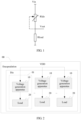
- FIG. 1 is a schematic diagram of a basic principle of a linear on-chip power supply in the prior art according to an embodiment in the present invention.
- stability of an output voltage Vout is maintained by adjusting an R1do resistor.
- R1do resistor In a circuit corresponding to FIG. 1 , it can be learned that a proportional relationship needs to be maintained between the R1do and an Rload to obtain an expected output voltage Vout. Therefore, in this implementation solution, practicability and flexibility of the power supply cannot be met.
- US application 2002/0014882 A1 discloses a linear regulator for providing the next stage with an output voltage.
- the linear regulator includes a first transistor, a first amplifier, a second transistor, and a second amplifier. When the output voltage at the output terminal is greater than a certain value, the second transistor conducts and sinks the current from the next stage.
- US application US 2014/0035550 A1 discloses a voltage regulator circuit including a plurality of transistors and a control circuit. Each transistor has two source/drain terminal and a gate terminal. One source/drain terminal of each transistor is electrically coupled to a source voltage, and the other source/drain terminals of the transistors are electrically coupled to each other and corporately referred to as an output terminal of the voltage regulator circuit.
- the object of the present invention is to provide a voltage generation apparatus and a semiconductor chip, so as to provide a good output voltage range when a load changes greatly. This object is solved by a voltage generation apparatus according to claim 1 and further advantageous embodiments and improvements are listed in the dependent claims.
- an embodiment of the present invention provides a voltage generation apparatus, including: a load, a controller, a first voltage division controller, a second voltage division controller, and a voltage detector, where the first voltage division controller and the load are connected in series between an input power supply and ground; the second voltage division controller and the load are connected in parallel between ground and a connection point between the first voltage division controller and the load; the voltage detector is electrically connected to the load, and is configured to: detect a load voltage of the load, and feed back a detected value of the load voltage to the controller; and the controller is electrically connected to the voltage detector, the first voltage division controller, and the second voltage division controller, and is configured to: receive the detected value fed back by the voltage detector, and generate a control signal based on the detected value, where the control signal is used to control the first voltage division controller and the second voltage division controller to adjust the load voltage to a target value, where when the detected value is greater than the target value, the control signal is used to execute at least one type of the following control: controlling a
- the first voltage division controller and the second voltage division controller includes multiple switch-controlled resistor sets, the multiple switch-controlled resistor sets are connected in parallel, each switch-controlled resistor set includes at least one parallel switch-controlled resistor, a primary switch-controlled resistor is controlled by a control bit in the control signal to control connection or disconnection of the switch-controlled resistor set, and multiple parallel control bits of the control signal are separately used to control connection or disconnection of the multiple switch-controlled resistor sets.
- the switch-controlled resistor set when the control bit controls the switch to be on, the switch-controlled resistor set is connected, and the resistor of the first voltage division controller or that of the second voltage division controller is controlled to decrease; or when the control bit controls the switch to be off, the switch-controlled resistor set is disconnected, and the resistor of the first voltage division controller or that of the second voltage division controller is controlled to increase.
- a switch of a Switch-controlled resistor in the first voltage division controller and a switch of a Switch-controlled resistor in the second voltage division controller are different types of transistors; and a control bit in the control signal received by the switch of the Switch-controlled resistor in the first voltage division controller and a control bit in the control signal received by the switch of the Switch-controlled resistor in the second voltage division controller have a same signal phase.
- control bit in the control signal received by the switch of the Switch-controlled resistor in the first voltage division controller and the control bit in the control signal received by the switch of the Switch-controlled resistor in the second voltage division controller are a same control bit.
- the different types of transistors are separately a P-channel metal-oxide semiconductor PMOS transistor and an N-channel metal-oxide semiconductor NMOS transistor.
- a switch of a Switch-controlled resistor in the first voltage division controller and a switch of a Switch-controlled resistor in the second voltage division controller are a same type of transistor; and a control bit in the control signal received by the switch of the Switch-controlled resistor in the first voltage division controller and a control bit in the control signal received by the switch of the Switch-controlled resistor in the second voltage division controller have opposite signal phases.
- the same type of transistor is a PMOS transistor or an NMOS transistor.
- the at least one switch-controlled resistor set includes N parallel switch-controlled resistors, each switch-controlled resistor includes a resistor and the switch that are connected in series, and N is a positive integer greater than or equal to 2, where in the N switch-controlled resistors, a control terminal of a switch of a primary switch-controlled resistor is configured to receive a control bit corresponding to the at least one switch-controlled resistor set; and in the N switch-controlled resistors, a control terminal of a switch of a current switch-controlled resistor is coupled to a connection point between a switch and a resistor that are connected in series in a previous switch-controlled resistor, and receives a signal output by the connection point, or the at least one switch-controlled resistor set includes N parallel switch-controlled resistor pairs, each switch-controlled resistor pair includes a pair of parallel switch-controlled resistors, each switch-controlled resistor includes a resistor and the switch that are connected in series, and N is a positive integer greater than or equal to 2, where in the N switch-
- a resistance of the resistor in the primary switch-controlled resistor is greater than a resistance of the resistor in the other switch-controlled resistor.
- At least one control bit of multiple parallel control bits of the control signal is used to: control at least one switch-controlled resistor set that is in the first voltage division controller and that corresponds to the at least one control bit, to change from disconnection to connection; or when the detected value is less than the target value, at least one control bit of multiple parallel control bits of the control signal is used to: control at least one switch-controlled resistor set that is in the first voltage division controller and that corresponds to the at least one control bit, to change connection to disconnection.
- At least one control bit of multiple parallel control bits of the control signal is used to: control at least one switch-controlled resistor set that is in the second voltage division controller and that corresponds to the at least one control bit, to change connection to disconnection; or when the detected value is less than the target value, at least one control bit of multiple parallel control bits of the control signal is used to: control at least one switch-controlled resistor set that is in the second voltage division controller and that corresponds to the at least one control bit, to change from disconnection to connection.
- the voltage detector includes a voltage information feedback unit, a voltage sampling and feedback unit, and a voltage encoding and feedback unit, where the voltage information feedback unit is configured to: read an analog load voltage of the load, and convert the voltage to a digital signal; the voltage sampling and feedback unit is configured to perform sampling on the digital signal based on a clock cycle, to obtain a voltage sampling signal; and the voltage encoding and feedback unit is configured to encode the voltage sampling signal, to obtain the detected value of the load voltage.
- the detected value is a binary serial number.
- an embodiment of the present invention provides a semiconductor chip, including a voltage generation apparatus and a load, where
- the voltage generation apparatus is provided, and the load voltage is adjusted by properly controlling the first voltage division controller and the second voltage division controller in the voltage generation apparatus, to reach the target value. In this way, a good output voltage range can be provided when the load or a load current changes greatly, and practicability is enhanced and extended.
- the terms “first”, “second”, “third”, “fourth”, and so on are intended to distinguish between different objects but do not indicate a particular order.
- the terms “including”, “having”, or any other variant thereof are intended to cover a non-exclusive inclusion.
- a process, a method, a system, a product, or a device that includes a series of steps or units is not limited to the listed steps or units, but optionally further includes an unlisted step or unit, or optionally further includes another inherent step or unit of the process, the method, the product, or the device.
- FIG. 2 is a schematic structural diagram of a chip of an on-chip integrated voltage generation apparatus according to an embodiment of the present invention.
- VDD for example, a battery
- the voltage generation apparatus 10 on the chip 00 generates a stable voltage with the power supplied by the VDD or as driven by the VDD, to supply power to the load 20 (for example, a logic circuit, a function module, a memory, or a processor) that is on the chip 00 and that is electrically connected to the chip 00.
- the load 20 for example, a logic circuit, a function module, a memory, or a processor
- the load 20 may perform various types of signal processing, for example, a module or a unit for processing a communications protocol, processing a voice conversion, processing a photographed image, or the like.
- the chip 00 shown in FIG. 2 may be used as some or all of various electronic apparatuses. This is not specifically limited in this embodiment of the present invention.
- the following describes in detail a specific structure and function of a power supply unit 01 that includes the voltage generation apparatus 10 on the chip 00 shown in FIG. 2 and the load 20 to which the voltage generation apparatus 10 supplies power.
- FIG. 3 is a schematic structural diagram of a power supply unit according to an embodiment of the present invention.
- the power supply unit 01 includes a voltage generation apparatus 10 and a load 20 to which the voltage generation apparatus 10 supplies power.
- the voltage generation apparatus 10 may include: a controller 100, a first voltage division controller 110, a second voltage division controller 120, and a voltage detector 130.
- the first voltage division controller 110 and the load 20 are connected in series between an input power supply VDD and ground.
- the second voltage division controller 120 and the load 20 are connected in parallel between ground and a connection point VVDD between the first voltage division controller 110 and the load 20. It can be learned that a voltage of the connection point VVDD reflects a load voltage.
- the voltage detector 130 is electrically connected to the load 20, and is configured to: detect a load voltage of the load 20 in real time, and feed back a detected value of the load voltage to the controller 100.
- the controller 100 is electrically connected to the voltage detector 130, the first voltage division controller 110, and the second voltage division controller 120, and is configured to: receive the detected value fed back by the voltage detector 130, and generate a control signal based on the detected value.
- the control signal is used to control the first voltage division controller 110 and the second voltage division controller 120 to adjust the load voltage to a target value.
- a control rule may mainly conform to the following principle: when the detected value is greater than the target value, the control signal is used to execute at least one type of the following control: controlling a resistance of the first voltage division controller to increase, or controlling a resistance of the second voltage division controller to decrease; or when the detected value is less than the target value, the control signal is used to execute at least one type of the following control: controlling a resistance of the first voltage division controller to decrease, or controlling a resistance of the second voltage division controller to increase.
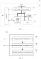
- FIG. 4 is a schematic structural diagram of a voltage detector according to an embodiment of the present invention.
- the voltage detector 130 is mainly responsible for detecting, in real time, a load voltage of a load 20 located on a chip, so as to effectively feed back a detected value of the load voltage to a controller 100. Therefore, in a possible implementation, the voltage detector 130 may include a voltage information feedback unit 1301, a voltage sampling and feedback unit 1302, and a voltage encoding and feedback unit 1303.
- the voltage information feedback unit 1301 is configured to: when an input terminal en terminal is enabled to access an enabling signal, read an original analog load voltage of the load, and convert the voltage to a digital signal.
- the voltage sampling and feedback unit 1302 is configured to: receive a clock clk signal, and perform, based on a clock cycle of the clock clk, sampling on the digital signal obtained after the conversion performed by the voltage information feedback unit 1301, to obtain a voltage sampling signal.
- the voltage encoding and feedback unit 1303 is configured to encode the voltage sampling signal that is fed back by the voltage sampling and feedback unit 1302, to obtain the detected value of the load voltage.
- the voltage detector 130 feeds back the detected value to the controller 100, so that the controller 100 receives the detected value fed back by the voltage detector 130, and generate a control signal based on the detected value.
- the control signal is used to control a first voltage division controller 110 and a second voltage division controller 120 to adjust the load voltage to a target value.
- the detected value may be a binary serial value.
- the voltage information feedback unit 1301 converts an analog voltage into a digital signal.
- the voltage sampling and feedback unit 1302 performs voltage sampling. A clock cycle of the sampling is greater than a clock cycle of outputting a digital signal by the voltage information feedback unit 1301. Therefore, a digital signal that changes more slowly than the original digital signal is obtained after the sampling.
- the voltage encoding and feedback unit 1303 is a format conversion unit, and is configured to convert, into a digital signal (that is, the detected value) that can be identified by the controller 100, the digital signal that is obtained after the sampling and that reflects the analog voltage. That is, the voltage encoding and feedback unit 1303 is equivalent to an encoder or a format converter.
- corresponding voltage detectors 130 may be set for different loads 20 according to a requirement so as to cover various application scenarios, for example, a scenario in which a voltage of each on-chip function module that consumes power is maintained stable.
- FIG. 5 is a schematic structural diagram of an embodiment of a voltage generation apparatus according to an embodiment of the present invention.
- the following describes in detail specific implementations of a first voltage division controller 110 and a second voltage division controller 120 of the voltage generation apparatus 10 in the present invention with reference to FIG. 3 and FIG. 5 .
- the first voltage division controller 110 and the second voltage division controller 120 of the voltage generation apparatus 10 are used as voltage regulation units in the voltage generation apparatus 10 in the embodiment corresponding to FIG. 3 , and may each include a switch-controlled resistor. Therefore, in a possible implementation, the first voltage division controller 110 or the second voltage division controller 120 may include multiple switch-controlled resistor sets ( FIG.
- each switch-controlled resistor set includes at least one parallel switch-controlled resistor.
- a primary switch-controlled resistor (for example, may be R1 of a first switch-controlled resistor in the switch-controlled resistor set 1101) is controlled by a control bit in the control signal (generated by the controller 100 in FIG.
- a resistance of the switch-controlled resistor set in the first voltage division controller 110 or a resistance of the switch-controlled resistor set in the second voltage division controller 120 in FIG. 5 decreases. That is, when the control bit IN controls the switch to be on, a resistor in the first voltage division controller changes from a disconnected state (in the disconnected state, the resistance is considered as infinite) to a connected state (a resistance in the connected state is a value of multiple sets of parallel resistors R1 and R2), and therefore the resistance decreases.
- a resistance of the first voltage division controller or that of the second voltage division controller is controlled to increase, that is, when the control bit IN controls the switch to be off, a resistor in the first voltage division controller changes from a connected state (a resistance in the connected state is a value of multiple groups of parallel resistors R1 and R2) to a disconnected state (in the disconnected state, the resistance is considered as infinite), and therefore the resistance increases.
- OUT output in the circuit corresponding to FIG. 5 reflects a current connected state of the voltage division controller (a switch-controlled resistor set), and an output control signal in the OUT may be directly fed back to the controller 100 in the embodiment corresponding to FIG.
- the controller 100 performs corresponding control according to feedback from the voltage detector 130 and according to a specific quantity of connected switch-controlled resistor sets in the first voltage division controller 110 and the second voltage division controller 120 or an operating state of switch-controlled resistor sets in the first voltage division controller 110 and the second voltage division controller 120.
- EN1 is effective (a high level)
- EN2 is also effective (a high level). That is, IN and OUT have a same phase.
- EN1 and EN2 are one after another in validity, that is, EN2 follows EN1.
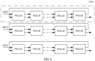
- FIG. 6 is a schematic structural diagram of multiple parallel PGCell sets according to an embodiment of the present invention.
- the multiple parallel PGCell sets in FIG. 6 are equivalent to a first voltage division controller 110 or a second voltage division controller 120.
- Each PGCell set (shown in a dashed-line box in FIG. 6 ) is equivalent to 1101 or 1201 in FIG.
- FIG. 5 shows multiple parallel PGCells.
- FIG. 6 shows at least three PGCell sets. The PGCell sets are in a parallel relationship. Each PGCell set includes at least one PGCell. When each PGCell set includes multiple PGCells, the multiple PGCells are connected in parallel. It may be understood that different voltages of a load 20 are obtained due to different quantities of connected PGCell sets. Therefore, when a voltage on the load 20 is unstable, a quantity of connected PGCell sets in the first voltage division controller 110 and/or in the second voltage division controller 120 may be controlled to maintain stability of the voltage on the load 20.
- the controller 100 receives various types of feedback information (including a detected value of a load voltage of a load) from the voltage detector 130, and controls the first voltage division controller 110 and/or the second voltage division controller 120 according to the feedback information, so as to ensure that a supply voltage of the load 20 is stable and reliable.
- various types of feedback information including a detected value of a load voltage of a load
- At least one control bit of multiple parallel control bits in a control signal generate by the controller 100 is used to: control at least one PGCell set that is in the first voltage division controller and that corresponds to at least one control bit, to change from disconnection to connection; or when the controller 100 determines that a detected value is less than a target value, at least one control bit of multiple parallel control bits in a control signal generate by the controller 100 is used to: control at least one PGCell set that is in the first voltage division controller and that corresponds to at least one control bit, to change connection to disconnection.
- a reason is that: when the controller 100 determines that a voltage on the load 20 is extremely low (less than a preset voltage threshold), a case in which the load 20 cannot normally operate may be caused, and therefore the voltage on the load 20 needs to be improved to the target value.
- the first voltage division controller 110 is connected to the load 20 in series, and a resistance of the load 20 is unchanged. Therefore, the voltage on the load 20 can be increased by increasing a current on the load 20. That is, a resistance of the first voltage division controller 110 may be reduced, to reduce a total series resistance of the first voltage division controller 110 and the load 20. Therefore, the current on the load 20 (and the voltage division controller 110) increases, and the voltage on the load 20 further increases.
- the first voltage division controller 110 is multiple parallel PGCell sets
- a quantity of connected parallel PGCell sets in the first voltage division controller is increased to reduce the resistance of the first voltage division controller 110, so as to stabilize the voltage on the load 20.
- at least one control bit of multiple parallel control bits of the control signal is used to: control at least one PGCell set that is in the second voltage division controller 120 and that corresponds to the at least one control bit, to change connection to disconnection; or when the detected value is less than the target value, at least one control bit of multiple parallel control bits of the control signal is used to: control at least one PGCell set that is in the second voltage division controller 120 and that corresponds to the at least one control bit, to change from disconnection to connection.
- a quantity of PGCells is not limited, may be one or more, and is determined based on a specific application scenario. When there is one PGCell, the PGCell set is equal to the PGCell.
- the voltage generation apparatus provided in the present invention not only can resolve a problem of an output voltage range when the load current is inaccurately estimated or is greatly different in different scenarios, but also can effectively suppress a large transient shock by using an on-chip integrated PGCell set, reduce an application risk, and improve quality of an on-chip power supply.
- the following describes in detail how the voltage generation apparatus provided in the present invention effectively suppresses a relatively large transient shock.
- FIG. 5 mainly shows a first voltage division controller 110 (only one PGCell set 1101 is drawn, a structure is similar to a structure used when there are multiple PGCell sets, and the PGCells are connected to each other in parallel), a second voltage division controller 120 (only one PGCell set 1201 is drawn, a structure is similar to a structure used when there are multiple PGCell sets, and the PGCells are connected to each other in parallel), and a load equivalent impedance Rload (that is, a load 20).
- VDD is an input power supply
- VVDD is a load voltage.
- the at least one PGCell set includes N (4 is shown in FIG.
- each switch-controlled resistor pair includes a pair of parallel switch-controlled resistors (for example, the first, a second, a third, and a fourth switch-controlled resistors), each switch-controlled resistor includes a resistor and the switch that are connected in series, and N is a positive integer greater than or equal to 2.
- N is a positive integer greater than or equal to 2.
- a control terminal for example, EN1 of R1 of the second switch-controlled resistor in the PGCell set 1101 in FIG. 5
- a switch of a primary switch-controlled resistor for example, R1 of the second switch-controlled resistor in 1101 in FIG. 5
- a current switch-controlled resistor pair for example, the second switch-controlled resistor in the PGCell set 1101 in FIG.
- connection point for example, ST1 of R1 of the first switch-controlled resistor in the PGCell set 1101 in FIG. 5
- a connection point for example, ST1 of R1 of the first switch-controlled resistor in the PGCell set 1101 in FIG. 5
- a control terminal EN2 of R2 of the fourth switch-controlled resistor in the PGCell set 1101 in FIG. 5
- ST1 of R1 of the fourth switch-controlled resistor in the PGCell set 1101 in FIG. 5 a control terminal of R2 of the fourth switch-controlled resistor in the PGCell set 1101 in FIG. 5
- a control terminal for example, EN2 of R2 of the third switch-controlled resistor in the PGCell set 1101 in FIG. 5
- a connection point for example, ST2 of R2 of the fourth switch-controlled resistor in the PGCell set 1101 in FIG. 5
- a switch-controlled resistor set that is, a PGCell set
- each switch-controlled resistor pair may also be replaced with a switch-controlled resistor.
- at least one switch-controlled resistor set (a PGCell set) in the first voltage division controller 110 or the second voltage division controller 120 of the voltage generation apparatus 10 includes N parallel switch-controlled resistors, each switch-controlled resistor includes a resistor and the switch that are connected in series, and N is a positive integer greater than or equal to 2.
- a control terminal of a switch of a primary switch-controlled resistor is configured to receive a control bit corresponding to the at least one switch-controlled resistor set.
- a control terminal of a switch of a current switch-controlled resistor is coupled to a connection point between a switch and a resistor that are connected in series in a previous switch-controlled resistor, and receives a signal output by the connection point.
- an operating principle is similar to that in FIG. 5 .
- Switch-controlled resistors in a switch-controlled resistor set can be sequentially powered on, to avoid a relatively large transient current shock and to prevent a surge.
- both large and small transistors are used. It is assumed that R1 is greater than R2. To suppress a system surge current, R1 and R2 are both extremely small in comparison with Rload. Therefore, multiple PGCell sets are connected in parallel, or multiple PGCells are connected in parallel in a PGCell set, so that VVDD is extremely close to VDD. It should be further noted that, when each PGCell (for example, an MTCMOS) in the first voltage division controller 110 is enabled, a channel resistance is generally tens of ohms, and when no PGCell is enabled, a resistance is generally greater than millions of ohms.
- PGCell for example, an MTCMOS
- switch-controlled switches in a resistor set (a PGCell set) in the first voltage division controller or the second voltage division controller are different types of transistors, and may be common power switches, transistors using a conventional CMOS process, or multi-threshold voltage CMOSs that are most frequently used in a power gating technology.
- the switch may include: a positive-channel metal-oxide semiconductor (PMOS) transistor, a negative-channel metal-oxide semiconductor (NMOS) transistor, or a multi-threshold voltage MTCMOS transistor.
- a switch of a PGCell in the first voltage division controller and a switch of a PGCell in the second voltage division controller are different types of transistors, for example, respectively a P-channel metal-oxide semiconductor PMOS transistor and an N-channel metal-oxide semiconductor NMOS transistor
- a control bit in the control signal received by the switch of the PGCell in the first voltage division controller and a control bit in the control signal received by the switch of the PGCell in the second voltage division controller have a same signal phase.
- the control bit in the control signal received by the switch of the PGCell in the first voltage division controller and the control bit in the control signal received by the switch of the PGCell in the second voltage division controller are a same control bit. In this way, the switch of the PGCell in the first voltage division controller and the switch of the PGCell in the second voltage division controller are not simultaneously on.
- a switch of a PGCell in the first voltage division controller and a switch of a PGCell in the second voltage division controller are a same type of transistor, for example, a PMOS transistor or an NMOS transistor
- a control bit in the control signal received by the switch of the PGCell in the first voltage division controller and a control bit in the control signal received by the switch of the PGCell in the second voltage division controller have opposite signal phases. It may be understood that a principle of the PMOS transistor and that of the NMOS transistor are similar, and only polarities controlled by gates are opposite. In this way, the switch of the PGCell in the first voltage division controller and the switch of the PGCell in the second voltage division controller are not simultaneously on.
- a quantity of PGCell sets in the first voltage division controller 110, a quantity of PGCell sets in the second voltage division controller 120, and a quantity of PGCells in the set are determined according to a design requirement.
- the quantity of PGCells sets in the first voltage division controller 110 may be the same as or different from a quantity of PGCell sets in the second voltage division controller 120, and the quantity of PGCells in a set may be the same as or different from the quantity of PGCells in another set.
- a voltage resolution and an adjustment range by using which the PGCell performs adjustment may be determined according to a design requirement in different solutions. This is not specifically limited in this embodiment of the present invention.
- a chip configuration process in the embodiments of the present invention may be as follows:
- connection relationship related in the embodiments is an electrical connection.
- the connection may be a direct connection by using a wire, or may be coupling in another manner according to an electric effect.
- the present invention further provides a semiconductor chip.
- the chip includes the voltage generation apparatus 10 and the load 20 that are provided in all the foregoing embodiments of the present invention.
- the load 20 operates under an action of the load voltage.
- the load is any one of a logic circuit, a functional circuit, a memory, or a processor. It may be understood that, for functions of all modules in the voltage generation apparatus 10, refer to the specific implementations in the apparatus embodiments in FIG. 1 to FIG. 6 . Details are not provided herein again.
Landscapes
- Engineering & Computer Science (AREA)
- Physics & Mathematics (AREA)
- Electromagnetism (AREA)
- General Physics & Mathematics (AREA)
- Radar, Positioning & Navigation (AREA)
- Automation & Control Theory (AREA)
- Power Engineering (AREA)
- Theoretical Computer Science (AREA)
- Dc-Dc Converters (AREA)
- Electronic Switches (AREA)
- Semiconductor Integrated Circuits (AREA)
- Control Of Voltage And Current In General (AREA)
Claims (11)
- Appareil de génération de tension comprenant : une charge (20), un contrôleur (100), un premier contrôleur de division de tension (110), un second contrôleur de division de tension (120), et un détecteur de tension (130), dans lequel :le premier contrôleur de division de tension (110) et la charge (20) sont connectés en série entre une alimentation d'entrée et la terre ;le second contrôleur de division de tension (120) et la charge (20) sont connectés en parallèle entre la terre et un point de connexion entre le premier contrôleur de division de tension (110) et la charge (20) ;le détecteur de tension (130) est connecté électriquement à la charge (20), et est configuré pour : détecter une tension de charge de la charge (20), et renvoyer une valeur détectée de la tension de charge au contrôleur (100) ; etle contrôleur (100) est connecté électriquement au détecteur de tension, au premier contrôleur de division de tension (110), et au second contrôleur de division de tension (120), et est configuré pour : recevoir la valeur détectée renvoyée par le détecteur de tension, et générer un signal de commande basé sur la valeur détectée, dans lequel le signal de commande est utilisé pour commander le premier contrôleur de division de tension (110) et le second contrôleur de division de tension pour ajuster la tension de charge à une valeur cible ;lorsque la valeur détectée est supérieure à la valeur cible, le signal de commande est utilisé pour exécuter au moins un type des commandes suivantes : commander une résistance du premier contrôleur de division de tension (110) pour l'augmenter, et commander une résistance du second contrôleur de division de tension (120) pour la diminuer ; etlorsque la valeur détectée est inférieure à la valeur cible, le signal de commande est utilisé pour exécuter au moins un type des commandes suivantes : commander une résistance du premier contrôleur de division de tension (110) pour la diminuer, et commander une résistance du second contrôleur de division de tension (120) pour l'augmenter ;dans lequel le premier contrôleur de division de tension (110) et le second contrôleur de division de tension (120) comprennent de multiples ensembles de résistances commandées par commutateur (1101, 1201), les multiples ensembles de résistances commandées par commutateur (1101, 1201) sont connectés en parallèle, chaque ensemble de résistances commandées par commutateur (1101, 1201) comprend au moins une résistance commandée par commutateur parallèle, une résistance commandée par commutateur primaire est commandée par un bit de commande dans le signal de commande pour commander la connexion ou la déconnexion de l'ensemble de résistances commandées par commutateur (1101, 1201), et de multiples bits de commande parallèles dans le signal de commande sont respectivement utilisés pour commander la connexion ou la déconnexion des multiples ensembles de résistances commandées par commutateur (1101, 1201) ;l'appareil étant caractérisé en ce que :au moins un ensemble de résistances commandées par commutateur (1101, 1201) comprend N résistances commandées par commutateur parallèles, chaque résistance commandée par commutateur comprend une résistance et un commutateur qui sont connectés en série, et N est un nombre entier positif supérieur ou égal à 2, dans lequel : dans les N résistances commandées par commutateur, une borne de commande d'un commutateur d'une résistance commandée par commutateur primaire est configurée pour recevoir un bit de commande correspondant à l' au moins un ensemble de résistances commandées par commutateur (1101, 1201) ; etdans les N résistances commandées par commutateur, une borne de commande d'un commutateur d'une résistance courante commandée par commutateur est couplée à un point de connexion entre un commutateur et une résistance qui sont connectés en série dans une résistance commandée par commutateur précédente, et reçoit un signal émis par le point de connexion ; oudans lequel l' au moins un ensemble de résistances commandées par commutateur (1101, 1201) comprend N paires de résistances commandées par commutateur parallèles, chaque paire de résistances commandées par commutateur comprend une paire de résistances commandées par commutateur parallèles, chaque résistance commandée par commutateur comprend une résistance et un commutateur qui sont connectés en série, et N est un nombre entier positif supérieur ou égal à 2, dans lequel :dans les N paires de résistances commandées par commutateur, une borne de commande d'un commutateur d'une résistance commandée par commutateur primaire dans une paire de résistances commandées par commutateur primaires est configurée pour recevoir un bit de commande correspondant à l'au moins un ensemble de résistances commandées par commutateur (1101, 1201) ;dans les N paires de résistances commandées par commutateur, une borne de commande d'un commutateur d'une résistance commandée par commutateur primaire dans une paire de résistances courantes commandées par commutateur est couplée à un point de connexion entre un commutateur et une résistance qui sont connectés en série dans une résistance commandée par commutateur primaire dans une paire de résistances commandées par commutateur précédentes, et reçoit un signal émis par le point de connexion ;dans les N paires de résistances commandées par commutateur, une borne de commande d'un commutateur de l'autre résistance commandée par commutateur dans la dernière paire de résistances commandées par commutateur est couplée à un point de connexion entre un commutateur et une résistance qui sont connectés en série dans une résistance primaire commandée par commutateur dans la dernière paire de résistances commandées par commutateur, et reçoit un signal émis par le point de connexion ; etdans les N paires de résistances commandées par commutateur, une borne de commande d'un commutateur de l'autre résistance commandée par commutateur dans la paire de résistances commandées par commutateur précédentes est couplée à un point de connexion entre un commutateur et une résistance qui sont connectés en série dans l'autre résistance commandée par commutateur dans la paire de résistances commandées par commutateur courantes, et reçoit un signal émis par le point de connexion.
- Appareil (10) selon la revendication 1, dans lequel :lorsque le bit de commande commande l'activation d'un commutateur, l'ensemble de résistances commandées par commutateur (1101, 1201) est connecté, et la résistance du premier contrôleur de division de tension (110) ou celle du second contrôleur de division de tension (120) est commandée pour diminuer ; oulorsque le bit de commande commande l'arrêt du commutateur, l'ensemble de résistances commandées par commutateur (1101, 1201) est déconnecté, et la résistance du premier contrôleur de division de tension (110) ou celle du second contrôleur de division de tension (120) est commandée pour augmenter.
- Appareil (10) selon la revendication 1 ou la revendication 2, dans lequel un commutateur d'une résistance commandée par commutateur dans le premier contrôleur de division de tension (110) et un commutateur d'une résistance commandée par commutateur dans le second contrôleur de division de tension (120) sont des types différents de transistors ; et
un bit de commande dans le signal de commande reçu par le commutateur de la résistance commandée par commutateur dans le premier contrôleur de division de tension (110) et un bit de commande dans le signal de commande reçu par le commutateur de la résistance commandée par commutateur dans le second contrôleur de division de tension (120) ont une même phase de signal. - Appareil (10) selon la revendication 3, dans lequel le bit de commande dans le signal de commande reçu par le commutateur de la résistance commandée par commutateur dans le premier contrôleur de division de tension (110) et le bit de commande dans le signal de commande reçu par le commutateur de la résistance commandée par commutateur dans le second contrôleur de division de tension (120) sont un même bit de commande.
- Appareil (10) selon la revendication 3 ou la revendication 4, dans lequel les différents types de transistors sont séparément un transistor métal-oxyde-semiconducteur à canal P, PMOS, et un transistor métal-oxyde-semiconducteur à canal N, NMOS.
- Appareil (10) selon la revendication 1 ou la revendication 2, dans lequel un commutateur d'une résistance commandée par commutateur dans le premier contrôleur de division de tension (110) et un commutateur d'une résistance commandée par commutateur dans le second contrôleur de division de tension (120) sont un même type de transistor ; et
un bit de commande dans le signal de commande reçu par le commutateur de la résistance commandée par commutateur dans le premier contrôleur de division de tension (110) et un bit de commande dans le signal de commande reçu par le commutateur de la résistance commandée par commutateur dans le second contrôleur de division de tension (120) ont des phases de signal opposées. - Appareil (10) selon la revendication 6, dans lequel le même type de transistor est un transistor PMOS ou un transistor NMOS.
- Appareil (10) selon la revendication 1, dans lequel dans toute paire de résistances commandées par commutateur, une résistance de la résistance dans la résistance primaire commandée par commutateur est supérieure à une résistance de la résistance dans l'autre résistance commandée par commutateur.
- Appareil (10) selon l'une quelconque des revendications 1 à 8, dans lequel :
lorsque la valeur détectée est supérieure à la valeur cible, au moins un bit de commande de multiples bits de commande parallèles du signal de commande est utilisé pour : commander au moins un ensemble de résistances commandées par commutateur (1101) qui est dans le premier contrôleur de division de tension (110) et qui correspond à l'au moins un bit de commande, pour passer de la déconnexion à la connexion ; ou lorsque la valeur détectée est inférieure à la valeur cible, au moins un bit de commande de multiples bits de commande parallèles du signal de commande est utilisé pour : commander au moins un ensemble de résistances commandées par commutateur (1101) qui est dans le premier contrôleur de division de tension (110) et qui correspond à l'au moins un bit de commande, pour passer de la connexion à la déconnexion. - Appareil (10) selon l'une quelconque des revendications 1 à 9, dans lequel :
lorsque la valeur détectée est supérieure à la valeur cible, au moins un bit de commande de multiples bits de commande parallèles du signal de commande est utilisé pour : commander au moins un ensemble de résistances commandées par commutateur (1201) qui est dans le second contrôleur de division de tension (120) et qui correspond à l'au moins un bit de commande, pour passer de la connexion à la déconnexion ; ou lorsque la valeur détectée est inférieure à la valeur cible, au moins un bit de commande de multiples bits de commande parallèles du signal de commande est utilisé pour : commander au moins un ensemble de résistances commandées par commutateur (1201) qui est dans le second contrôleur de division de tension (120) et qui correspond à l'au moins un bit de commande, pour passer de la déconnexion à la connexion. - Appareil (10) selon l'une quelconque des revendications 1 à 10, dans lequel le détecteur de tension (130) comprend une unité de retour d'informations de tension (1301), une unité d'échantillonnage de tension et de rétroaction (1302), et une unité de codage de tension et de rétroaction (1303), dans lequel :l'unité de retour d'informations de tension (1301) est configurée pour : lire une tension de charge analogique de la charge (20), et convertir la tension en un signal numérique ; l'unité d'échantillonnage de tension et de rétroaction (1302) est configurée pour effectuer un échantillonnage sur le signal numérique sur la base d'un cycle d'horloge, pour obtenir un signal d'échantillonnage de tension ; etl'unité de codage de tension et de rétroaction (1303) est configurée pour coder le signal d'échantillonnage de tension, pour obtenir la valeur détectée de la tension de charge.
Applications Claiming Priority (2)
| Application Number | Priority Date | Filing Date | Title |
|---|---|---|---|
| CN201610685888.6A CN106292827B (zh) | 2016-08-18 | 2016-08-18 | 一种电压产生装置及半导体芯片 |
| PCT/CN2017/078420 WO2018032766A1 (fr) | 2016-08-18 | 2017-03-28 | Dispositif de génération de tension et puce semi-conductrice |
Publications (3)
| Publication Number | Publication Date |
|---|---|
| EP3447603A1 EP3447603A1 (fr) | 2019-02-27 |
| EP3447603A4 EP3447603A4 (fr) | 2019-06-26 |
| EP3447603B1 true EP3447603B1 (fr) | 2023-05-10 |
Family
ID=57679982
Family Applications (1)
| Application Number | Title | Priority Date | Filing Date |
|---|---|---|---|
| EP17840743.3A Active EP3447603B1 (fr) | 2016-08-18 | 2017-03-28 | Dispositif de génération de tension et puce semi-conductrice |
Country Status (5)
| Country | Link |
|---|---|
| US (1) | US10345835B2 (fr) |
| EP (1) | EP3447603B1 (fr) |
| KR (1) | KR20190002680A (fr) |
| CN (2) | CN106292827B (fr) |
| WO (1) | WO2018032766A1 (fr) |
Families Citing this family (3)
| Publication number | Priority date | Publication date | Assignee | Title |
|---|---|---|---|---|
| CN106292827B (zh) | 2016-08-18 | 2018-09-21 | 华为技术有限公司 | 一种电压产生装置及半导体芯片 |
| JP6830385B2 (ja) * | 2017-03-24 | 2021-02-17 | エイブリック株式会社 | 半導体回路 |
| CN114518777B (zh) * | 2020-11-19 | 2024-09-13 | 启碁科技股份有限公司 | 具有可动态配置反馈电压的电压调节电路 |
Family Cites Families (52)
| Publication number | Priority date | Publication date | Assignee | Title |
|---|---|---|---|---|
| JPS6051716B2 (ja) * | 1977-06-13 | 1985-11-15 | 株式会社東芝 | 電圧分割回路 |
| US5219228A (en) * | 1992-05-11 | 1993-06-15 | General Motors Corporation | Exhaust gas temperature measuring system utilizing existing oxygen sensor |
| US5657422A (en) * | 1994-01-28 | 1997-08-12 | Lucent Technologies Inc. | Voice activity detection driven noise remediator |
| JP3516556B2 (ja) * | 1996-08-02 | 2004-04-05 | 沖電気工業株式会社 | 内部電源回路 |
| US5953218A (en) * | 1997-06-19 | 1999-09-14 | Canon Kabushiki Kaisha | High voltage generation apparatus |
| KR100278096B1 (ko) * | 1997-07-10 | 2001-01-15 | 윤덕용 | 혼합형 레귤레이터 |
| US5966004A (en) * | 1998-02-17 | 1999-10-12 | Motorola, Inc. | Electronic system with regulator, and method |
| US6259237B1 (en) | 1998-11-04 | 2001-07-10 | Lockheed Martin Corporation | Method and apparatus for providing high current power regulation |
| US6429709B1 (en) * | 1998-12-14 | 2002-08-06 | Semiconductor Components Industries Llc | Power converter circuit and method for controlling |
| US6377033B2 (en) * | 2000-08-07 | 2002-04-23 | Asustek Computer Inc. | Linear regulator capable of sinking current |
| JP4504536B2 (ja) * | 2000-08-29 | 2010-07-14 | ルネサスエレクトロニクス株式会社 | 出力制御装置及び出力制御方法 |
| US6775164B2 (en) * | 2002-03-14 | 2004-08-10 | Tyco Electronics Corporation | Three-terminal, low voltage pulse width modulation controller IC |
| US6713991B1 (en) * | 2002-04-24 | 2004-03-30 | Rantec Power Systems Inc. | Bipolar shunt regulator |
| EP1367703A1 (fr) * | 2002-05-31 | 2003-12-03 | STMicroelectronics S.r.l. | Méthode pour régler la tension d'alimentation d'une charge et régulateur de tension correspondant |
| US7106037B2 (en) * | 2003-07-02 | 2006-09-12 | Toko, Inc. | Switching-type constant current power supply device |
| US7116063B2 (en) * | 2003-07-28 | 2006-10-03 | Matsushita Electric Works, Ltd. | Dimmable discharge lamp lighting device |
| US6937180B1 (en) * | 2004-04-26 | 2005-08-30 | Texas Instruments Incorporated | Code-controlled voltage divider |
| US7208919B2 (en) * | 2005-05-17 | 2007-04-24 | Sigmatel, Inc. | Method and apparatus for digitally regulating an output voltage using noise-shaped component selection |
| DE102005045530B4 (de) * | 2005-09-23 | 2016-03-31 | Infineon Technologies Ag | Verfahren zur Spannungsregelung einer Halbleiterschaltung sowie entsprechende Spannungsregelvorrichtung und Halbleiterschaltung |
| DE102006007479B4 (de) * | 2006-02-17 | 2017-08-10 | Infineon Technologies Ag | Shunt-Regler |
| JP4740771B2 (ja) * | 2006-03-03 | 2011-08-03 | 株式会社リコー | 分圧回路、その分圧回路を使用した定電圧回路及び電圧検出回路、分圧回路のトリミング方法 |
| US20070262760A1 (en) * | 2006-05-09 | 2007-11-15 | Kwang-Hwa Liu | Multiple-output dc-dc converter |
| CN101644937B (zh) * | 2008-08-04 | 2011-11-16 | 新德科技股份有限公司 | 一种利用可调式熔丝调整参考电压的电路 |
| CN101791733B (zh) * | 2009-10-31 | 2012-05-30 | 华南理工大学 | 一种铝合金双丝双脉冲焊接方法及其焊接电源 |
| CN201533275U (zh) * | 2009-11-20 | 2010-07-21 | 南京格致电力技术有限公司 | 负载电压或电流的调节装置 |
| JP5786368B2 (ja) * | 2010-03-05 | 2015-09-30 | 富士電機株式会社 | 入力電圧検出回路を備えたデジタル制御スイッチング電源装置 |
| JP5437871B2 (ja) | 2010-03-18 | 2014-03-12 | セイコーインスツル株式会社 | 分圧回路及び半導体装置 |
| WO2011148926A1 (fr) * | 2010-05-28 | 2011-12-01 | 三洋電機株式会社 | Dispositif d'alimentation électrique |
| CN102566633B (zh) * | 2010-12-07 | 2014-02-12 | 华邦电子股份有限公司 | 低压差稳压器 |
| DE102011056141A1 (de) * | 2010-12-20 | 2012-06-21 | Samsung Electronics Co., Ltd. | Negativspannungsgenerator, Dekoder, nicht-flüchtige Speichervorrichtung und Speichersystem, das eine negative Spannung verwendet |
| US8817500B2 (en) * | 2011-02-17 | 2014-08-26 | Samsung Electronics Co., Ltd. | Power supply apparatuses for preventing latch-up of charge pump and methods thereof |
| JP5431396B2 (ja) * | 2011-03-10 | 2014-03-05 | 株式会社東芝 | 定電圧電源回路 |
| WO2013038583A1 (fr) * | 2011-09-14 | 2013-03-21 | パナソニック株式会社 | Dispositif à semiconducteur et système d'alimentation électrique muni de celui-ci |
| KR20130030096A (ko) * | 2011-09-16 | 2013-03-26 | 삼성전자주식회사 | 전력 제어 회로, 이를 포함하는 반도체 장치 및 상기 전력 제어 회로의 동작방법 |
| TWI561951B (en) * | 2012-01-30 | 2016-12-11 | Semiconductor Energy Lab Co Ltd | Power supply circuit |
| US8970197B2 (en) * | 2012-08-03 | 2015-03-03 | United Microelectronics Corporation | Voltage regulating circuit configured to have output voltage thereof modulated digitally |
| CN103854695B (zh) * | 2012-11-30 | 2017-02-08 | 英业达科技有限公司 | 电压产生装置 |
| CN103869852B (zh) * | 2012-12-18 | 2016-10-19 | 宏碁股份有限公司 | 电压调节装置与电子设备 |
| CN104238609A (zh) * | 2013-06-14 | 2014-12-24 | 鸿富锦精密工业(深圳)有限公司 | 电压调整电路 |
| CN104124971B (zh) * | 2013-11-08 | 2018-06-05 | 西安电子科技大学 | 基于逐次逼近原理的两级流水线型模数转换器 |
| CN203798884U (zh) * | 2014-04-25 | 2014-08-27 | 湖南银河电气有限公司 | 一种新型分压器 |
| CN104281183B (zh) * | 2014-08-25 | 2016-04-27 | 南京航空航天大学 | 一种基于模糊反馈的非接触电能传输稳压系统 |
| CN105449643B (zh) * | 2014-08-28 | 2018-08-07 | 联想(北京)有限公司 | 一种保护电路及电子设备 |
| JP6324919B2 (ja) * | 2015-03-17 | 2018-05-16 | ミネベアミツミ株式会社 | モータ駆動制御装置及びその制御方法 |
| CN104850210B (zh) * | 2015-04-30 | 2017-12-01 | 华为技术有限公司 | 一种电源门控电路 |
| CN204615656U (zh) * | 2015-05-28 | 2015-09-02 | 西安科技大学 | 一种可调式开关电源 |
| CN105142293B (zh) * | 2015-09-16 | 2017-12-26 | 英特格灵芯片(天津)有限公司 | 一种反馈驱动电路 |
| US9584033B1 (en) * | 2015-10-19 | 2017-02-28 | Chicony Power Technology Co., Ltd. | Power supply device for varying an output voltage |
| CN205176716U (zh) * | 2015-11-30 | 2016-04-20 | 龙芯中科技术有限公司 | 电压调整电路、设备和系统 |
| US10033284B2 (en) * | 2016-06-10 | 2018-07-24 | Power Integrations, Inc. | Power supply with power factor correction and output-referenced energy reservoir |
| CN106292827B (zh) * | 2016-08-18 | 2018-09-21 | 华为技术有限公司 | 一种电压产生装置及半导体芯片 |
| CN106849620B (zh) * | 2016-12-30 | 2019-09-13 | 华为技术有限公司 | 电压调整方法、控制器和芯片 |
-
2016
- 2016-08-18 CN CN201610685888.6A patent/CN106292827B/zh active Active
- 2016-08-18 CN CN201810891448.5A patent/CN109032233A/zh active Pending
-
2017
- 2017-03-28 KR KR1020187035232A patent/KR20190002680A/ko not_active Withdrawn
- 2017-03-28 EP EP17840743.3A patent/EP3447603B1/fr active Active
- 2017-03-28 WO PCT/CN2017/078420 patent/WO2018032766A1/fr not_active Ceased
-
2018
- 2018-12-19 US US16/226,421 patent/US10345835B2/en active Active
Also Published As
| Publication number | Publication date |
|---|---|
| WO2018032766A1 (fr) | 2018-02-22 |
| CN109032233A (zh) | 2018-12-18 |
| CN106292827B (zh) | 2018-09-21 |
| EP3447603A4 (fr) | 2019-06-26 |
| US20190121380A1 (en) | 2019-04-25 |
| US10345835B2 (en) | 2019-07-09 |
| EP3447603A1 (fr) | 2019-02-27 |
| CN106292827A (zh) | 2017-01-04 |
| KR20190002680A (ko) | 2019-01-08 |
Similar Documents
| Publication | Publication Date | Title |
|---|---|---|
| US10423179B2 (en) | Low drop out regulator compatible with type C USB standard | |
| US9454164B2 (en) | Method and apparatus for limiting startup inrush current for low dropout regulator | |
| US9525407B2 (en) | Power monitoring circuit, and a power up reset generator | |
| US9148056B2 (en) | Voltage regulation system for integrated circuit | |
| US9651958B2 (en) | Circuit for regulating startup and operation voltage of an electronic device | |
| US9977475B2 (en) | Over voltage protection for a communication line of a bus | |
| US8975776B2 (en) | Fast start-up voltage regulator | |
| US10345835B2 (en) | Voltage generation apparatus and semiconductor chip | |
| EP3251150B1 (fr) | Interrupteur de protection à courant inverse à auto-détection | |
| US7639041B1 (en) | Hotsocket-compatible body bias circuitry with power-up current reduction capabilities | |
| US20180284822A1 (en) | Low leakage low dropout regulator with high bandwidth and power supply rejection | |
| US20070069819A1 (en) | Transistor drive circuit, constant voltage circuit, and method thereof using a plurality of error amplifying circuits to effectively drive a power transistor | |
| EP3462274A1 (fr) | Dispositifs à semi-conducteurs pour détecter des tensions | |
| US9946278B2 (en) | Droop detection for low-dropout regulator | |
| US9429968B2 (en) | Power-gated electronic device | |
| US11139807B2 (en) | Buffer circuit | |
| TW201115872A (en) | Electrical-overstress protection circuit for an integrated circuit | |
| US9608633B1 (en) | Interface circuit with configurable variable supply voltage for transmitting signals | |
| CN105515555B (zh) | 采用脉冲触发方式实现主电路上电的启动电路 | |
| US10509428B1 (en) | Circuit with multiple voltage scaling power switches | |
| EP2650747A1 (fr) | Dispositif électronique à déclenchement d'alimentation et son procédé de fonctionnement | |
| CN108776501B (zh) | Ldo和por的复用电路 | |
| EP3644508B1 (fr) | Commutateur à courant inverse | |
| CN119002619A (zh) | 基于低压器件的耐压缓冲电路及芯片 | |
| US8653859B2 (en) | Electronic comparison circuit |
Legal Events
| Date | Code | Title | Description |
|---|---|---|---|
| STAA | Information on the status of an ep patent application or granted ep patent |
Free format text: STATUS: THE INTERNATIONAL PUBLICATION HAS BEEN MADE |
|
| PUAI | Public reference made under article 153(3) epc to a published international application that has entered the european phase |
Free format text: ORIGINAL CODE: 0009012 |
|
| STAA | Information on the status of an ep patent application or granted ep patent |
Free format text: STATUS: REQUEST FOR EXAMINATION WAS MADE |
|
| 17P | Request for examination filed |
Effective date: 20181119 |
|
| AK | Designated contracting states |
Kind code of ref document: A1 Designated state(s): AL AT BE BG CH CY CZ DE DK EE ES FI FR GB GR HR HU IE IS IT LI LT LU LV MC MK MT NL NO PL PT RO RS SE SI SK SM TR |
|
| AX | Request for extension of the european patent |
Extension state: BA ME |
|
| REG | Reference to a national code |
Ref country code: DE Ref legal event code: R079 Ref document number: 602017068700 Country of ref document: DE Free format text: PREVIOUS MAIN CLASS: G05F0001656000 Ipc: G05F0001618000 |
|
| A4 | Supplementary search report drawn up and despatched |
Effective date: 20190528 |
|
| RIC1 | Information provided on ipc code assigned before grant |
Ipc: G05F 1/618 20060101AFI20190522BHEP |
|
| DAV | Request for validation of the european patent (deleted) | ||
| DAX | Request for extension of the european patent (deleted) | ||
| STAA | Information on the status of an ep patent application or granted ep patent |
Free format text: STATUS: EXAMINATION IS IN PROGRESS |
|
| 17Q | First examination report despatched |
Effective date: 20210302 |
|
| GRAP | Despatch of communication of intention to grant a patent |
Free format text: ORIGINAL CODE: EPIDOSNIGR1 |
|
| STAA | Information on the status of an ep patent application or granted ep patent |
Free format text: STATUS: GRANT OF PATENT IS INTENDED |
|
| INTG | Intention to grant announced |
Effective date: 20221125 |
|
| GRAS | Grant fee paid |
Free format text: ORIGINAL CODE: EPIDOSNIGR3 |
|
| GRAA | (expected) grant |
Free format text: ORIGINAL CODE: 0009210 |
|
| STAA | Information on the status of an ep patent application or granted ep patent |
Free format text: STATUS: THE PATENT HAS BEEN GRANTED |
|
| AK | Designated contracting states |
Kind code of ref document: B1 Designated state(s): AL AT BE BG CH CY CZ DE DK EE ES FI FR GB GR HR HU IE IS IT LI LT LU LV MC MK MT NL NO PL PT RO RS SE SI SK SM TR |
|
| REG | Reference to a national code |
Ref country code: GB Ref legal event code: FG4D |
|
| REG | Reference to a national code |
Ref country code: AT Ref legal event code: REF Ref document number: 1567314 Country of ref document: AT Kind code of ref document: T Effective date: 20230515 Ref country code: CH Ref legal event code: EP |
|
| REG | Reference to a national code |
Ref country code: DE Ref legal event code: R096 Ref document number: 602017068700 Country of ref document: DE |
|
| REG | Reference to a national code |
Ref country code: IE Ref legal event code: FG4D |
|
| P01 | Opt-out of the competence of the unified patent court (upc) registered |
Effective date: 20230524 |
|
| REG | Reference to a national code |
Ref country code: LT Ref legal event code: MG9D |
|
| REG | Reference to a national code |
Ref country code: NL Ref legal event code: MP Effective date: 20230510 |
|
| REG | Reference to a national code |
Ref country code: AT Ref legal event code: MK05 Ref document number: 1567314 Country of ref document: AT Kind code of ref document: T Effective date: 20230510 |
|
| PG25 | Lapsed in a contracting state [announced via postgrant information from national office to epo] |
Ref country code: SE Free format text: LAPSE BECAUSE OF FAILURE TO SUBMIT A TRANSLATION OF THE DESCRIPTION OR TO PAY THE FEE WITHIN THE PRESCRIBED TIME-LIMIT Effective date: 20230510 Ref country code: PT Free format text: LAPSE BECAUSE OF FAILURE TO SUBMIT A TRANSLATION OF THE DESCRIPTION OR TO PAY THE FEE WITHIN THE PRESCRIBED TIME-LIMIT Effective date: 20230911 Ref country code: NO Free format text: LAPSE BECAUSE OF FAILURE TO SUBMIT A TRANSLATION OF THE DESCRIPTION OR TO PAY THE FEE WITHIN THE PRESCRIBED TIME-LIMIT Effective date: 20230810 Ref country code: NL Free format text: LAPSE BECAUSE OF FAILURE TO SUBMIT A TRANSLATION OF THE DESCRIPTION OR TO PAY THE FEE WITHIN THE PRESCRIBED TIME-LIMIT Effective date: 20230510 Ref country code: ES Free format text: LAPSE BECAUSE OF FAILURE TO SUBMIT A TRANSLATION OF THE DESCRIPTION OR TO PAY THE FEE WITHIN THE PRESCRIBED TIME-LIMIT Effective date: 20230510 Ref country code: AT Free format text: LAPSE BECAUSE OF FAILURE TO SUBMIT A TRANSLATION OF THE DESCRIPTION OR TO PAY THE FEE WITHIN THE PRESCRIBED TIME-LIMIT Effective date: 20230510 |
|
| PG25 | Lapsed in a contracting state [announced via postgrant information from national office to epo] |
Ref country code: RS Free format text: LAPSE BECAUSE OF FAILURE TO SUBMIT A TRANSLATION OF THE DESCRIPTION OR TO PAY THE FEE WITHIN THE PRESCRIBED TIME-LIMIT Effective date: 20230510 Ref country code: PL Free format text: LAPSE BECAUSE OF FAILURE TO SUBMIT A TRANSLATION OF THE DESCRIPTION OR TO PAY THE FEE WITHIN THE PRESCRIBED TIME-LIMIT Effective date: 20230510 Ref country code: LV Free format text: LAPSE BECAUSE OF FAILURE TO SUBMIT A TRANSLATION OF THE DESCRIPTION OR TO PAY THE FEE WITHIN THE PRESCRIBED TIME-LIMIT Effective date: 20230510 Ref country code: LT Free format text: LAPSE BECAUSE OF FAILURE TO SUBMIT A TRANSLATION OF THE DESCRIPTION OR TO PAY THE FEE WITHIN THE PRESCRIBED TIME-LIMIT Effective date: 20230510 Ref country code: IS Free format text: LAPSE BECAUSE OF FAILURE TO SUBMIT A TRANSLATION OF THE DESCRIPTION OR TO PAY THE FEE WITHIN THE PRESCRIBED TIME-LIMIT Effective date: 20230910 Ref country code: HR Free format text: LAPSE BECAUSE OF FAILURE TO SUBMIT A TRANSLATION OF THE DESCRIPTION OR TO PAY THE FEE WITHIN THE PRESCRIBED TIME-LIMIT Effective date: 20230510 Ref country code: GR Free format text: LAPSE BECAUSE OF FAILURE TO SUBMIT A TRANSLATION OF THE DESCRIPTION OR TO PAY THE FEE WITHIN THE PRESCRIBED TIME-LIMIT Effective date: 20230811 |
|
| PG25 | Lapsed in a contracting state [announced via postgrant information from national office to epo] |
Ref country code: FI Free format text: LAPSE BECAUSE OF FAILURE TO SUBMIT A TRANSLATION OF THE DESCRIPTION OR TO PAY THE FEE WITHIN THE PRESCRIBED TIME-LIMIT Effective date: 20230510 |
|
| PG25 | Lapsed in a contracting state [announced via postgrant information from national office to epo] |
Ref country code: SK Free format text: LAPSE BECAUSE OF FAILURE TO SUBMIT A TRANSLATION OF THE DESCRIPTION OR TO PAY THE FEE WITHIN THE PRESCRIBED TIME-LIMIT Effective date: 20230510 |
|
| PG25 | Lapsed in a contracting state [announced via postgrant information from national office to epo] |
Ref country code: SM Free format text: LAPSE BECAUSE OF FAILURE TO SUBMIT A TRANSLATION OF THE DESCRIPTION OR TO PAY THE FEE WITHIN THE PRESCRIBED TIME-LIMIT Effective date: 20230510 Ref country code: SK Free format text: LAPSE BECAUSE OF FAILURE TO SUBMIT A TRANSLATION OF THE DESCRIPTION OR TO PAY THE FEE WITHIN THE PRESCRIBED TIME-LIMIT Effective date: 20230510 Ref country code: RO Free format text: LAPSE BECAUSE OF FAILURE TO SUBMIT A TRANSLATION OF THE DESCRIPTION OR TO PAY THE FEE WITHIN THE PRESCRIBED TIME-LIMIT Effective date: 20230510 Ref country code: EE Free format text: LAPSE BECAUSE OF FAILURE TO SUBMIT A TRANSLATION OF THE DESCRIPTION OR TO PAY THE FEE WITHIN THE PRESCRIBED TIME-LIMIT Effective date: 20230510 Ref country code: DK Free format text: LAPSE BECAUSE OF FAILURE TO SUBMIT A TRANSLATION OF THE DESCRIPTION OR TO PAY THE FEE WITHIN THE PRESCRIBED TIME-LIMIT Effective date: 20230510 Ref country code: CZ Free format text: LAPSE BECAUSE OF FAILURE TO SUBMIT A TRANSLATION OF THE DESCRIPTION OR TO PAY THE FEE WITHIN THE PRESCRIBED TIME-LIMIT Effective date: 20230510 |
|
| REG | Reference to a national code |
Ref country code: DE Ref legal event code: R097 Ref document number: 602017068700 Country of ref document: DE |
|
| PLBE | No opposition filed within time limit |
Free format text: ORIGINAL CODE: 0009261 |
|
| STAA | Information on the status of an ep patent application or granted ep patent |
Free format text: STATUS: NO OPPOSITION FILED WITHIN TIME LIMIT |
|
| 26N | No opposition filed |
Effective date: 20240213 |
|
| PG25 | Lapsed in a contracting state [announced via postgrant information from national office to epo] |
Ref country code: SI Free format text: LAPSE BECAUSE OF FAILURE TO SUBMIT A TRANSLATION OF THE DESCRIPTION OR TO PAY THE FEE WITHIN THE PRESCRIBED TIME-LIMIT Effective date: 20230510 |
|
| PG25 | Lapsed in a contracting state [announced via postgrant information from national office to epo] |
Ref country code: SI Free format text: LAPSE BECAUSE OF FAILURE TO SUBMIT A TRANSLATION OF THE DESCRIPTION OR TO PAY THE FEE WITHIN THE PRESCRIBED TIME-LIMIT Effective date: 20230510 Ref country code: IT Free format text: LAPSE BECAUSE OF FAILURE TO SUBMIT A TRANSLATION OF THE DESCRIPTION OR TO PAY THE FEE WITHIN THE PRESCRIBED TIME-LIMIT Effective date: 20230510 |
|
| REG | Reference to a national code |
Ref country code: CH Ref legal event code: PL |
|
| PG25 | Lapsed in a contracting state [announced via postgrant information from national office to epo] |
Ref country code: BG Free format text: LAPSE BECAUSE OF FAILURE TO SUBMIT A TRANSLATION OF THE DESCRIPTION OR TO PAY THE FEE WITHIN THE PRESCRIBED TIME-LIMIT Effective date: 20230510 |
|
| PG25 | Lapsed in a contracting state [announced via postgrant information from national office to epo] |
Ref country code: LU Free format text: LAPSE BECAUSE OF NON-PAYMENT OF DUE FEES Effective date: 20240328 |
|
| PG25 | Lapsed in a contracting state [announced via postgrant information from national office to epo] |
Ref country code: MC Free format text: LAPSE BECAUSE OF FAILURE TO SUBMIT A TRANSLATION OF THE DESCRIPTION OR TO PAY THE FEE WITHIN THE PRESCRIBED TIME-LIMIT Effective date: 20230510 |
|
| PG25 | Lapsed in a contracting state [announced via postgrant information from national office to epo] |
Ref country code: MC Free format text: LAPSE BECAUSE OF FAILURE TO SUBMIT A TRANSLATION OF THE DESCRIPTION OR TO PAY THE FEE WITHIN THE PRESCRIBED TIME-LIMIT Effective date: 20230510 Ref country code: LU Free format text: LAPSE BECAUSE OF NON-PAYMENT OF DUE FEES Effective date: 20240328 Ref country code: BG Free format text: LAPSE BECAUSE OF FAILURE TO SUBMIT A TRANSLATION OF THE DESCRIPTION OR TO PAY THE FEE WITHIN THE PRESCRIBED TIME-LIMIT Effective date: 20230510 |
|
| REG | Reference to a national code |
Ref country code: BE Ref legal event code: MM Effective date: 20240331 |
|
| PG25 | Lapsed in a contracting state [announced via postgrant information from national office to epo] |
Ref country code: BE Free format text: LAPSE BECAUSE OF NON-PAYMENT OF DUE FEES Effective date: 20240331 |
|
| PG25 | Lapsed in a contracting state [announced via postgrant information from national office to epo] |
Ref country code: FR Free format text: LAPSE BECAUSE OF NON-PAYMENT OF DUE FEES Effective date: 20240331 |
|
| PG25 | Lapsed in a contracting state [announced via postgrant information from national office to epo] |
Ref country code: IE Free format text: LAPSE BECAUSE OF NON-PAYMENT OF DUE FEES Effective date: 20240328 |
|
| PG25 | Lapsed in a contracting state [announced via postgrant information from national office to epo] |
Ref country code: IE Free format text: LAPSE BECAUSE OF NON-PAYMENT OF DUE FEES Effective date: 20240328 Ref country code: FR Free format text: LAPSE BECAUSE OF NON-PAYMENT OF DUE FEES Effective date: 20240331 Ref country code: BE Free format text: LAPSE BECAUSE OF NON-PAYMENT OF DUE FEES Effective date: 20240331 Ref country code: CH Free format text: LAPSE BECAUSE OF NON-PAYMENT OF DUE FEES Effective date: 20240331 |
|
| PG25 | Lapsed in a contracting state [announced via postgrant information from national office to epo] |
Ref country code: CY Free format text: LAPSE BECAUSE OF FAILURE TO SUBMIT A TRANSLATION OF THE DESCRIPTION OR TO PAY THE FEE WITHIN THE PRESCRIBED TIME-LIMIT; INVALID AB INITIO Effective date: 20170328 |
|
| PG25 | Lapsed in a contracting state [announced via postgrant information from national office to epo] |
Ref country code: HU Free format text: LAPSE BECAUSE OF FAILURE TO SUBMIT A TRANSLATION OF THE DESCRIPTION OR TO PAY THE FEE WITHIN THE PRESCRIBED TIME-LIMIT; INVALID AB INITIO Effective date: 20170328 |
|
| PG25 | Lapsed in a contracting state [announced via postgrant information from national office to epo] |
Ref country code: TR Free format text: LAPSE BECAUSE OF FAILURE TO SUBMIT A TRANSLATION OF THE DESCRIPTION OR TO PAY THE FEE WITHIN THE PRESCRIBED TIME-LIMIT Effective date: 20230510 |
|
| PGFP | Annual fee paid to national office [announced via postgrant information from national office to epo] |
Ref country code: GB Payment date: 20260209 Year of fee payment: 10 |
|
| PGFP | Annual fee paid to national office [announced via postgrant information from national office to epo] |
Ref country code: DE Payment date: 20260204 Year of fee payment: 10 |