EP3447860B1 - Halbleiterbauelementherstellungsverfahren - Google Patents
Halbleiterbauelementherstellungsverfahren Download PDFInfo
- Publication number
- EP3447860B1 EP3447860B1 EP16899364.0A EP16899364A EP3447860B1 EP 3447860 B1 EP3447860 B1 EP 3447860B1 EP 16899364 A EP16899364 A EP 16899364A EP 3447860 B1 EP3447860 B1 EP 3447860B1
- Authority
- EP
- European Patent Office
- Prior art keywords
- connector
- integrally molded
- molded article
- frontage
- connection terminal
- Prior art date
- Legal status (The legal status is an assumption and is not a legal conclusion. Google has not performed a legal analysis and makes no representation as to the accuracy of the status listed.)
- Not-in-force
Links
Images


Classifications
-
- H—ELECTRICITY
- H01—ELECTRIC ELEMENTS
- H01R—ELECTRICALLY-CONDUCTIVE CONNECTIONS; STRUCTURAL ASSOCIATIONS OF A PLURALITY OF MUTUALLY-INSULATED ELECTRICAL CONNECTING ELEMENTS; COUPLING DEVICES; CURRENT COLLECTORS
- H01R43/00—Apparatus or processes specially adapted for manufacturing, assembling, maintaining, or repairing of line connectors or current collectors or for joining electric conductors
- H01R43/20—Apparatus or processes specially adapted for manufacturing, assembling, maintaining, or repairing of line connectors or current collectors or for joining electric conductors for assembling or disassembling contact members with insulating base, case or sleeve
- H01R43/24—Assembling by moulding on contact members
-
- H—ELECTRICITY
- H01—ELECTRIC ELEMENTS
- H01R—ELECTRICALLY-CONDUCTIVE CONNECTIONS; STRUCTURAL ASSOCIATIONS OF A PLURALITY OF MUTUALLY-INSULATED ELECTRICAL CONNECTING ELEMENTS; COUPLING DEVICES; CURRENT COLLECTORS
- H01R43/00—Apparatus or processes specially adapted for manufacturing, assembling, maintaining, or repairing of line connectors or current collectors or for joining electric conductors
- H01R43/18—Apparatus or processes specially adapted for manufacturing, assembling, maintaining, or repairing of line connectors or current collectors or for joining electric conductors for manufacturing bases or cases for contact members
-
- H—ELECTRICITY
- H01—ELECTRIC ELEMENTS
- H01R—ELECTRICALLY-CONDUCTIVE CONNECTIONS; STRUCTURAL ASSOCIATIONS OF A PLURALITY OF MUTUALLY-INSULATED ELECTRICAL CONNECTING ELEMENTS; COUPLING DEVICES; CURRENT COLLECTORS
- H01R13/00—Details of coupling devices of the kinds covered by groups H01R12/70 or H01R24/00 - H01R33/00
- H01R13/46—Bases; Cases
- H01R13/502—Bases; Cases composed of different pieces
- H01R13/504—Bases; Cases composed of different pieces different pieces being moulded, cemented, welded, e.g. ultrasonic welding, or swaged together
-
- H—ELECTRICITY
- H01—ELECTRIC ELEMENTS
- H01R—ELECTRICALLY-CONDUCTIVE CONNECTIONS; STRUCTURAL ASSOCIATIONS OF A PLURALITY OF MUTUALLY-INSULATED ELECTRICAL CONNECTING ELEMENTS; COUPLING DEVICES; CURRENT COLLECTORS
- H01R13/00—Details of coupling devices of the kinds covered by groups H01R12/70 or H01R24/00 - H01R33/00
- H01R13/46—Bases; Cases
- H01R13/514—Bases; Cases composed as a modular blocks or assembly, i.e. composed of co-operating parts provided with contact members or holding contact members between them
-
- H—ELECTRICITY
- H01—ELECTRIC ELEMENTS
- H01R—ELECTRICALLY-CONDUCTIVE CONNECTIONS; STRUCTURAL ASSOCIATIONS OF A PLURALITY OF MUTUALLY-INSULATED ELECTRICAL CONNECTING ELEMENTS; COUPLING DEVICES; CURRENT COLLECTORS
- H01R13/00—Details of coupling devices of the kinds covered by groups H01R12/70 or H01R24/00 - H01R33/00
- H01R13/46—Bases; Cases
- H01R13/52—Dustproof, splashproof, drip-proof, waterproof, or flameproof cases
- H01R13/5202—Sealing means between parts of housing or between housing part and a wall, e.g. sealing rings
-
- H—ELECTRICITY
- H01—ELECTRIC ELEMENTS
- H01R—ELECTRICALLY-CONDUCTIVE CONNECTIONS; STRUCTURAL ASSOCIATIONS OF A PLURALITY OF MUTUALLY-INSULATED ELECTRICAL CONNECTING ELEMENTS; COUPLING DEVICES; CURRENT COLLECTORS
- H01R43/00—Apparatus or processes specially adapted for manufacturing, assembling, maintaining, or repairing of line connectors or current collectors or for joining electric conductors
- H01R43/005—Apparatus or processes specially adapted for manufacturing, assembling, maintaining, or repairing of line connectors or current collectors or for joining electric conductors for making dustproof, splashproof, drip-proof, waterproof, or flameproof connection, coupling, or casing
-
- H—ELECTRICITY
- H01—ELECTRIC ELEMENTS
- H01R—ELECTRICALLY-CONDUCTIVE CONNECTIONS; STRUCTURAL ASSOCIATIONS OF A PLURALITY OF MUTUALLY-INSULATED ELECTRICAL CONNECTING ELEMENTS; COUPLING DEVICES; CURRENT COLLECTORS
- H01R2201/00—Connectors or connections adapted for particular applications
- H01R2201/26—Connectors or connections adapted for particular applications for vehicles
Definitions
- the present invention relates to a connector device manufacturing method.
- Connectors are handled in fields in which various electrical connections are carried out, and are used in order to improve a flow of power or a signal.
- connectors provide an advantage in organizing electrical wiring by a multiple of connectors being integrated in a place in which a large number of electrical wires are disposed in a complex manner.
- a multiple of wiring structures are integrated, and a multiple of connectors are configured by molding using an insulating resin (Patent Document 1).
- a connector housing is configured by a multiple of connectors with differing frontage forms (terminal disposition patterns) being integrated, and installed in a control device (Patent Document 2).
- Patent Document 3 is concerned with a method of producing a device connector and Patent Document 6 is concerned with an electronic control device.
- a connector housing When a connector housing is configured by a multiple of connectors being integrated, wiring can be organized, because of which there is an advantage in that a maintenance operation becomes easier. Also, because connector frontage forms differ, an advantage is obtained in that a wiring connection error is prevented.
- an existing connector device is such that a connector connection terminal, a connector frontage, and a connector housing are of an integrated structure (a connector housing assembly), resin is injected into a periphery of a metal part forming the connector connection terminal, and a formation method that integrates the metal and the resin is adopted. Because of this, for example, when changing the form of the connector frontage only without changing the form of the connector connection terminal or the connector housing, or when changing the disposition of the connector frontage, a molding die for forming the whole connector device needs to be newly fabricated, and there is a problem in that time is needed for fabricating the molding die, and a problem in that costs for molding die fabrication increase.
- the invention has an object of resolving the previously described problems, and providing a connector device manufacturing method such that a change in design of a connector device can be carried out swiftly, and moreover, costs can be kept low.
- a connector device manufacturing method of the invention is defined in claim 1.
- specifications of various forms of a connector frontage of a connector device can be responded to by changing only the connector frontage, whereby part standardization can be achieved.
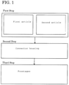
- a connector device manufacturing method of the invention is configured of a first process of fabricating a first integrally molded article having a first connector connection terminal and a second integrally molded article having a second connector connection terminal, a second process of forming a connector housing by integrating the first integrally molded article and the second integrally molded article, and a third process of forming a first connector frontage corresponding to the first integrally molded article and a second connector frontage corresponding to the second integrally molded article in the connector housing.
- connector connection terminals of various forms are prepared, and integrally molded articles are fabricated, wherein peripheries of the connector connection terminals are hardened using resin.
- integrally molded articles are fabricated by each of connector connection terminals including a connector connection terminal for power supply wiring and a connector connection terminal for signal wiring being hardened with resin.
- a multiple of the integrally molded articles including the various connector connection terminals fabricated in the first process are gathered and formed into an assembly, further hardened with resin and integrated, thereby forming a connector housing.
- a multiple of various kinds of connector connection terminal, or a multiple of the same kind of connector connection terminal are arbitrarily combined, and integrated by hardening with resin.
- a connector frontage individually specified in advance is formed in accordance with each connector connection terminal integrated in the connector housing.
- insert molding is carried out by individual molding dies corresponding to the connector frontages specified in accordance with the connector connection terminals being used in combination, thereby forming the connector frontage in accordance with each connector connection terminal in the connector housing.
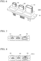
- a connector device manufactured via the processes shown in Fig. 1 is used by being installed in a kind of vehicle-use control device 100 shown in Fig. 2 . That is, the vehicle-use control device 100 shown in Fig. 2 is the integrated vehicle-use control device 100 wherein a motor 101 and a control device 102 are integrated, and a connector device 103 shown in Fig. 3 is installed in the vehicle-use control device 100.
- the connector device 103 shown in Fig. 3 is commonly called an external connection connector, and as a structure thereof, a first connector connection terminal 11 and a second connector connection terminal 12 are integrated with a connector housing 20, a first connector frontage 31, and a second connector frontage 32.
- the first connector connection terminal 11 and the second connector connection terminal 12 are electrically connected to the control device 102 shown in Fig. 2 .
- wiring (not shown) from an exterior is connected to the first connector frontage 31 and the second connector frontage 32. That is, the connector device 103 electrically connects the wiring from the exterior and the control device 102.
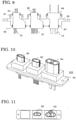
- Fig. 4 Using Fig. 4 , a description will be given adopting a case in which there are three kinds of connector connection terminal.
- the case shown in Fig. 4 being multiple kinds of connector connection terminal fabricated using the first process of the first embodiment of the invention, is such that the first connector connection terminal 11, the second connector connection terminal 12, and a third connector connection terminal 13 are each insert molded, and a connector connection terminal (power supply) integrally molded article 41 and connector connection terminal (signal) integrally molded articles 42 and 43 are fabricated.
- the connector connection terminal (power supply) integrally molded article 41 and the connector connection terminal (signal) integrally molded articles 42 and 43 are insert molded so as to be enclosed in the connector housing 20, thereby fabricating a connector housing assembly (connector housing component) 50.
- the fabricated connector housing assembly 50 is shown in Fig. 5 .
- first connector frontage 61 molding of a first connector frontage 61, a second connector frontage 62, and a third connector frontage 63 is carried out in accordance with the connector connection terminal (power supply) integrally molded article 41 and the connector connection terminal (signal) integrally molded articles 42 and 43 respectively, and integrated with the connector housing assembly 50, whereby the connector device 103 is completed, as shown in Fig. 6 .
- the connector device 103 completed in the third process is such that the first connector frontage 61 is a two pin-compatible connector, the second connector frontage 62 is a ten pin-compatible connector, and the third connector frontage 63 is a six pin-compatible connector.
- a fourth connector connection terminal 14 in accordance with the fourth connector frontage 64 is insert molded using resin, thereby fabricating a fourth connector connection terminal (power supply) integrally molded article 44.
- a connector connection terminal 15 in accordance with the fifth connector frontage 65 is insert molded, thereby fabricating the third connector connection terminal (signal) integrally molded article 43.
- the connector connection terminal (signal) integrally molded article 42 used in the external connection connector 103 is diverted for use as the connector connection terminal (signal) integrally molded article in accordance with the connector frontage 63.
- the connector connection terminal (power supply) integrally molded article 44 and the connector connection terminal (signal) integrally molded articles 42 and 43 are integrally molded using the same molding die as for the connector housing 20 used in the external connection connector 103, thereby fabricating the connector housing assembly 50.
- the fourth connector frontage 64, the third connector frontage 63, and the fifth connector frontage 65 are molded, and integrated with the connector housing assembly 50, whereby the connector device 103 is completed, as shown in Fig. 10 .
- a molding die is newly fabricated for the fourth connector frontage 64 and the fifth connector frontage 65, but the molding die for the second connector frontage 62 used in the connector device 103 is diverted to be used for the third connector frontage 63.
- the reason the second connector frontage 62 can be diverted to be used is that external connection connector seal portions 91 shown in Fig. 9 are of the same form.
- a molded article dummy 45 in which no connector connection terminal is inserted is fabricated for use as a portion in which no connector is provided. This has a function of leaking resin when molding the connector housing 20.
- an overall form and volume (both excluding the connector connection terminal portion) of the connector connection terminal (signal) integrally molded article resin portion are the same, in the same way as the connector connection terminal integrally molded articles.
- the connector connection terminal (power supply) integrally molded article 44 for the fourth connector frontage 64 used in the connector device 103 and the connector connection terminal (signal) integrally molded article 42 for the second connector frontage 62 used in the connector device 103 are diverted for use as the connector connection terminal integrally molded articles.
- the connector connection terminal (power supply) integrally molded article 44, the connector connection terminal (signal) integrally molded article 42, and the dummy 45 are integrally molded using the same molding die as for the connector housing 20 used in the external connection connector 103, thereby fabricating the connector housing assembly 50.
- molding of the fourth connector frontage 64, the second connector frontage 62, and a connector cover 66 is carried out, and integrated with the connector housing assembly 50, whereby the external connection connector 103A is completed, as shown in Fig. 14 .
- a molding die is newly fabricated for the connector cover 66, but the molding die for the fourth connector frontage 64 used in the external connection connector 103A is diverted to be used for the fourth connector frontage 64, and the molding die for the second connector frontage 62 used in the external connection connector 103A is diverted to be used for the second connector frontage 62.
- the molding die for the connector cover 66 fabricated here can also be diverted to be used elsewhere.
- a first method is shown in Fig. 15 .
- a labyrinth form 32 is provided in the connector housing assembly resin portion 30. Owing to the labyrinth form 32, a creepage distance to the resin interface 31 after molding of a connector frontage 33 is secured, whereby maintaining of airtightness is realized.
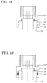
- a second method is shown in Fig. 16 as another method of maintaining airtightness.
- a rib leading end 34 of the connector housing assembly resin portion 30 is formed in an easily-melted form by being configured more thinly than another portion, or the like, whereby the rib leading end 34 is melted when molding the connector frontage 33, the connector housing assembly resin portion 30 and the connector frontage 33 are integrated, and airtightness of the resin interface 31 is maintained.
- a third method is shown in Fig. 17 as another method.
- a seal groove 35 of an uneven structure is provided in the connector housing assembly resin portion 30, and a sealing agent 36 is applied all along the seal groove 35.
- the connector frontage 33 is molded, and airtightness of the resin interface 31 is maintained.
- a sealing agent 36A is applied all over a resin interface between the connector housing assembly resin portion 30 and the connector frontage 33 after the connector frontage 33 is molded in the connector housing assembly resin portion 30, whereby airtightness of the resin interface 31 is maintained.
- a fourth method is shown in Fig. 19 as another method. Heat is applied in a post-processing after the connector housing assembly resin portion 30 and the connector frontage 33 are molded, sealing an interface by subjecting the connector housing assembly resin portion 30 and the connector frontage 33 to a melting 37, and maintaining airtightness of the resin interface 31.
- a connector housing assembly molding die can be diverted for use elsewhere even when only a kind of connector frontage form of the connector device (external connection connector) 103 is changed. Also, a connector frontage molding die, and a connector connection terminal and a connector connection terminal integrally molded article corresponding thereto, can also be diverted for use elsewhere. Furthermore, measures can also be taken when airtightness needs to be maintained, as shown in Fig. 15 to Fig. 19 .
Landscapes
- Engineering & Computer Science (AREA)
- Manufacturing & Machinery (AREA)
- Manufacturing Of Electrical Connectors (AREA)
- Connector Housings Or Holding Contact Members (AREA)
- Injection Moulding Of Plastics Or The Like (AREA)
Claims (6)
- Herstellungsverfahren einer Verbindervorrichtung (103, 103A), aufweisend:einen ersten Schritt zur Herstellung eines ersten integral ausgebildeten Formteils (41, 42, 43, 44), das eine erste Verbinderanschlussklemme (11, 12, 13, 14) aufweist, und eines zweiten integral ausgebildeten Formteils (41, 42, 43, 44), das eine zweite Verbinderanschlussklemme (11, 12, 13, 14) aufweist, indem sowohl die erste und die zweite Verbinderanschlussklemme (11, 12, 13, 14) mit einem Harz gehärtet werden;einen zweiten Schritt zur Ausbildung eines Verbindergehäuses (20, 30, 50) durch Integrieren des ersten integral ausgebildeten Formteils (41, 42, 43, 44) und des zweiten integral ausgebildeten Formteils (41, 42, 43, 44), wobei das erste und das zweite integral ausgebildete Formteil (41, 42, 43, 44) eingegossen werden, sodass sie in dem Verbindergehäuse (20, 30, 50) eingefasst sind; undeinen dritten Schritt zur Ausbildung einer ersten Verbinderfront (61, 62, 63, 64, 65) entsprechend dem ersten integral ausgebildeten Formteil (41, 42, 43, 44) und einer zweiten Verbinderfront (61, 62, 63, 64, 65) entsprechend dem zweiten integral ausgebildeten Formteil (41, 42, 43, 44) in dem Verbindergehäuse (20, 30, 50).
- Herstellungsverfahren einer Verbindervorrichtung (103, 103A) gemäß Anspruch 1,wobei ein äußerer Umfangsabschnitt des ersten integral ausgebildeten Formteils (41, 42, 43, 44) und des zweiten integral ausgebildeten Formteils (41, 42, 43, 44) eine Labyrinth-Struktur (32) mit einer ungleichmäßigen Form aufweist,wobei eine Aufrechterhaltung von Luftdichtigkeit in dem dritten Schritt ausgeführt wird.
- Herstellungsverfahren einer Verbindervorrichtung (103, 103A) gemäß Anspruch 1,wobei ein äußerer Umfangsabschnitt des ersten integral ausgebildeten Formteils (41, 42, 43, 44) und des zweiten integral ausgebildeten Formteils (41, 42, 43, 44) einen Rippenabschnitt (34) mit einer rippenartigen Struktur aufweist,wobei eine Aufrechterhaltung von Luftdichtigkeit in dem dritten Schritt durch Verursachen von Schmelzen des Rippenabschnitts (34) während des Integrierens mit dem Verbindergehäuse (30) ausgeführt wird.
- Herstellungsverfahren einer Verbindervorrichtung (103, 103A) gemäß Anspruch 1,wobei ein äußerer Umfangsabschnitt des ersten integral ausgebildeten Formteils (41, 42, 43, 44) und des zweiten integral ausgebildeten Formteils (41, 42, 43, 44) eine Dichtungsnut (35) mit einer ungleichmäßigen Struktur aufweist,wobei ein Dichtungsmittel (36) auf der Dichtungsnut (35) während des Integrierens mit dem Verbindergehäuse (30) aufgebracht wird und eine Aufrechterhaltung von Luftdichtigkeit in dem dritten Schritt ausgeführt wird.
- Herstellungsverfahren einer Verbindervorrichtung (103, 103A) gemäß Anspruch 1,
wobei, wenn die Verbinderfront (61, 62, 63, 64, 65) mit dem Verbindergehäuse (30) integriert wird, eine Grenzfläche zwischen den beiden (37) geschmolzen wird. - Herstellungsverfahren einer Verbindervorrichtung (103, 103A) gemäß Anspruch 1,
wobei das erste integral ausgebildete Formteil (41, 42, 43, 44), das zweite integral ausgebildete Formteil (41, 42, 43, 44) und ein Dummy-Formteil (45), das keine Verbinderanschlussklemme aufweist, hergestellt werden, das Verbindergehäuse (50) durch Integrieren des ersten integral ausgebildeten Formteils (41, 42, 43, 44), des zweiten integral ausgebildeten Formteils (41, 42, 43, 44) und des Dummy-Formteils (45) ausgebildet wird, und die erste Verbinderfront (61, 62, 63, 64, 65) und die zweite Verbinderfront (61, 62, 63, 64, 65) entsprechend dem ersten integral ausgebildeten Formteil (41, 42, 43, 44) und dem zweiten integral ausgebildeten Formteil (41, 42, 43, 44) in dem Verbindergehäuse (50) ausgebildet werden.
Applications Claiming Priority (1)
| Application Number | Priority Date | Filing Date | Title |
|---|---|---|---|
| PCT/JP2016/062303 WO2017183090A1 (ja) | 2016-04-19 | 2016-04-19 | コネクタ装置の製造方法 |
Publications (3)
| Publication Number | Publication Date |
|---|---|
| EP3447860A1 EP3447860A1 (de) | 2019-02-27 |
| EP3447860A4 EP3447860A4 (de) | 2019-07-03 |
| EP3447860B1 true EP3447860B1 (de) | 2022-01-19 |
Family
ID=60116629
Family Applications (1)
| Application Number | Title | Priority Date | Filing Date |
|---|---|---|---|
| EP16899364.0A Not-in-force EP3447860B1 (de) | 2016-04-19 | 2016-04-19 | Halbleiterbauelementherstellungsverfahren |
Country Status (5)
| Country | Link |
|---|---|
| US (2) | US11152755B2 (de) |
| EP (1) | EP3447860B1 (de) |
| JP (1) | JP6516926B2 (de) |
| CN (1) | CN109075519B (de) |
| WO (1) | WO2017183090A1 (de) |
Families Citing this family (6)
| Publication number | Priority date | Publication date | Assignee | Title |
|---|---|---|---|---|
| DE102017000722A1 (de) * | 2017-01-27 | 2018-08-02 | Thyssenkrupp Ag | Herstellung eines abgedichteten Steckers durch Verpressen von Klebstoff während des Fügens von Steckerkontakten und Steckergehäuse |
| CN110290670B (zh) * | 2019-07-19 | 2024-05-17 | 宁波伯骏智能科技有限公司 | 一种电控盒及其制造方法 |
| KR102528103B1 (ko) * | 2020-11-10 | 2023-05-03 | 주식회사 삼현 | 소형 모터 모듈용 하우징 제조 방법 |
| DE102021117009B3 (de) * | 2021-07-01 | 2022-09-29 | Lisa Dräxlmaier GmbH | Steckverbindungseinrichtung und verfahren zum montieren einer steckverbindungseinrichtung |
| DE102021121465A1 (de) * | 2021-08-18 | 2023-02-23 | Borgwarner Inc. | Leiterplattenverbindungsvorrichtung und Leiterplattenanordnung |
| JP2025515525A (ja) * | 2022-05-09 | 2025-05-20 | ヤザキ ノース アメリカ,インコーポレイテッド | 適合ピンアダプタ板 |
Family Cites Families (22)
| Publication number | Priority date | Publication date | Assignee | Title |
|---|---|---|---|---|
| JPS53116490A (en) * | 1977-03-22 | 1978-10-11 | Omron Tateisi Electronics Co | Preparing terminal device |
| JP3176496B2 (ja) * | 1993-12-27 | 2001-06-18 | シャープ株式会社 | 光結合装置およびその製造方法 |
| TW443011B (en) * | 1998-10-29 | 2001-06-23 | Hon Hai Prec Ind Co Ltd | Method for making an electrical connector |
| JP4028151B2 (ja) * | 2000-03-02 | 2007-12-26 | 矢崎総業株式会社 | コネクタ |
| JP2002231375A (ja) * | 2001-01-30 | 2002-08-16 | Yazaki Corp | 補機モジュールの封止構造 |
| CN1469516A (zh) * | 2002-07-15 | 2004-01-21 | 台捷电子股份有限公司 | 电连接器的制造方法 |
| US6824426B1 (en) * | 2004-02-10 | 2004-11-30 | Hon Hai Precision Ind. Co., Ltd. | High speed electrical cable assembly |
| JP4551166B2 (ja) | 2004-09-13 | 2010-09-22 | 矢崎総業株式会社 | 機器直付けコネクタ |
| JP4849323B2 (ja) | 2006-07-13 | 2012-01-11 | 住友電装株式会社 | インサート成形品の製造方法およびインサート成形用の成形型 |
| JP2008135683A (ja) * | 2006-10-24 | 2008-06-12 | Sharp Corp | 光結合装置およびその製造方法、並びに、光結合装置を用いた電子機器 |
| US7833025B2 (en) * | 2008-09-30 | 2010-11-16 | Symbol Technologies, Inc. | Sealed, solderless I/O connector |
| JP5503991B2 (ja) * | 2010-02-03 | 2014-05-28 | 矢崎総業株式会社 | コネクタ端子の製造方法及び多段コネクタの組立方法 |
| DE112011103017B4 (de) * | 2010-09-09 | 2017-10-05 | Autonetworks Technologies, Ltd. | Elektronische Schaltkreiseinheit zur Anordnung an einem Automatikgetriebe eines Fahrzeugs sowie Herstellungsverfahren hierfür |
| JP5641345B2 (ja) * | 2011-03-15 | 2014-12-17 | 住友電装株式会社 | 機器用コネクタ |
| JP5526096B2 (ja) * | 2011-09-21 | 2014-06-18 | 日立オートモティブシステムズ株式会社 | 電子制御装置のシール構造 |
| JP5789494B2 (ja) * | 2011-11-24 | 2015-10-07 | 矢崎総業株式会社 | コネクタ及びコネクタの製造方法 |
| JP5377710B2 (ja) * | 2012-05-24 | 2013-12-25 | 三菱電機株式会社 | 制御装置、及び制御装置一体型回転電機 |
| US20140030556A1 (en) * | 2012-07-30 | 2014-01-30 | Delphi Technologies, Inc. | Circuit board to circuit board connector with vertical and longitudinal assembly alignment features |
| DE102013204149A1 (de) | 2013-03-11 | 2014-09-25 | Robert Bosch Gmbh | Verfahren zum Herstellen einer modularen elektrischen Steckerverbinderanordnung für ein Steuergerät in einem Kraftfahrzeug |
| JP6443081B2 (ja) * | 2015-01-28 | 2018-12-26 | 住友電装株式会社 | コネクタ装置 |
| US10027051B1 (en) * | 2017-02-20 | 2018-07-17 | Robert Bosch Gmbh | Hybrid electrical connector |
| JP7006206B2 (ja) * | 2017-12-05 | 2022-01-24 | 住友電装株式会社 | コネクタ組付体 |
-
2016
- 2016-04-19 JP JP2018512668A patent/JP6516926B2/ja not_active Expired - Fee Related
- 2016-04-19 EP EP16899364.0A patent/EP3447860B1/de not_active Not-in-force
- 2016-04-19 US US16/085,678 patent/US11152755B2/en not_active Expired - Fee Related
- 2016-04-19 CN CN201680084531.0A patent/CN109075519B/zh not_active Expired - Fee Related
- 2016-04-19 WO PCT/JP2016/062303 patent/WO2017183090A1/ja not_active Ceased
-
2021
- 2021-07-15 US US17/376,969 patent/US20210344156A1/en not_active Abandoned
Non-Patent Citations (1)
| Title |
|---|
| None * |
Also Published As
| Publication number | Publication date |
|---|---|
| EP3447860A1 (de) | 2019-02-27 |
| EP3447860A4 (de) | 2019-07-03 |
| JPWO2017183090A1 (ja) | 2018-06-07 |
| WO2017183090A1 (ja) | 2017-10-26 |
| US20190097375A1 (en) | 2019-03-28 |
| CN109075519B (zh) | 2020-06-26 |
| US11152755B2 (en) | 2021-10-19 |
| CN109075519A (zh) | 2018-12-21 |
| US20210344156A1 (en) | 2021-11-04 |
| JP6516926B2 (ja) | 2019-05-22 |
Similar Documents
| Publication | Publication Date | Title |
|---|---|---|
| US20210344156A1 (en) | Connector device manufacturing method | |
| CN104953753B (zh) | 车载用角型连接器一体化伺服马达的连接器及其制造方法 | |
| JP6107362B2 (ja) | 半導体装置の製造方法及び半導体装置 | |
| US20120198933A1 (en) | Connection Assembly for a Sensor Assembly and Sensor Assembly | |
| JP6442527B2 (ja) | 電子制御装置 | |
| KR101759049B1 (ko) | 플라스틱 사출 오버몰드 전도체 경로 구조 및 플라스틱 사출 오버몰드 전도체 경로 구조를 제조하기 위한 방법 | |
| US11276962B2 (en) | Connector and manufacturing method thereof | |
| CN104836360A (zh) | 定子绕组端部绝缘框架、塑封定子总成及塑封电机 | |
| US9808973B2 (en) | Insert-moulded lead frame and method for the production thereof | |
| JP2016148652A (ja) | 電流センサの作製方法 | |
| US9849848B2 (en) | Motor vehicle component support and method for the production thereof | |
| CN104836389A (zh) | 防止绝缘框架大面积外露的方法及塑封定子总成 | |
| US11660793B2 (en) | Conductive member module, and production method therefor | |
| CN110731042A (zh) | 电子部件及其生产方法 | |
| JP6605417B2 (ja) | 樹脂成形品及びその製造方法 | |
| CN103015815B (zh) | 闭锁器及闭锁器的制作方法 | |
| KR101909248B1 (ko) | 버스바조립체 및 그 제조방법 | |
| CN107107414B (zh) | 生产具有一个外壳部件和至少两个导体的组件的方法 | |
| EP3091641B1 (de) | Zugentlastungsanordnung für einen elektrischen leiter und verfahren zur erzeugung einer zugentlastung für einen elektrischen leiter | |
| JP5677541B1 (ja) | インシュレータおよびインシュレータの製造方法 | |
| JP2013008709A (ja) | 樹脂モールド型コンデンサの製造方法 | |
| JP2015115546A (ja) | 実装品及びその製造方法 | |
| JP2014146559A (ja) | 集合型電気コネクタ及び集合型電気コネクタ製造方法 |
Legal Events
| Date | Code | Title | Description |
|---|---|---|---|
| STAA | Information on the status of an ep patent application or granted ep patent |
Free format text: STATUS: THE INTERNATIONAL PUBLICATION HAS BEEN MADE |
|
| PUAI | Public reference made under article 153(3) epc to a published international application that has entered the european phase |
Free format text: ORIGINAL CODE: 0009012 |
|
| STAA | Information on the status of an ep patent application or granted ep patent |
Free format text: STATUS: REQUEST FOR EXAMINATION WAS MADE |
|
| 17P | Request for examination filed |
Effective date: 20181008 |
|
| AK | Designated contracting states |
Kind code of ref document: A1 Designated state(s): AL AT BE BG CH CY CZ DE DK EE ES FI FR GB GR HR HU IE IS IT LI LT LU LV MC MK MT NL NO PL PT RO RS SE SI SK SM TR |
|
| AX | Request for extension of the european patent |
Extension state: BA ME |
|
| A4 | Supplementary search report drawn up and despatched |
Effective date: 20190604 |
|
| RIC1 | Information provided on ipc code assigned before grant |
Ipc: H01R 43/18 20060101ALN20190528BHEP Ipc: H01R 13/504 20060101ALI20190528BHEP Ipc: H01R 13/514 20060101ALI20190528BHEP Ipc: H01R 43/24 20060101AFI20190528BHEP |
|
| DAV | Request for validation of the european patent (deleted) | ||
| DAX | Request for extension of the european patent (deleted) | ||
| STAA | Information on the status of an ep patent application or granted ep patent |
Free format text: STATUS: EXAMINATION IS IN PROGRESS |
|
| 17Q | First examination report despatched |
Effective date: 20200921 |
|
| GRAP | Despatch of communication of intention to grant a patent |
Free format text: ORIGINAL CODE: EPIDOSNIGR1 |
|
| RIC1 | Information provided on ipc code assigned before grant |
Ipc: H01R 43/18 20060101ALN20210923BHEP Ipc: H01R 13/504 20060101ALI20210923BHEP Ipc: H01R 13/514 20060101ALI20210923BHEP Ipc: H01R 43/24 20060101AFI20210923BHEP |
|
| STAA | Information on the status of an ep patent application or granted ep patent |
Free format text: STATUS: GRANT OF PATENT IS INTENDED |
|
| RIC1 | Information provided on ipc code assigned before grant |
Ipc: H01R 43/18 20060101ALN20210930BHEP Ipc: H01R 13/504 20060101ALI20210930BHEP Ipc: H01R 13/514 20060101ALI20210930BHEP Ipc: H01R 43/24 20060101AFI20210930BHEP |
|
| RIC1 | Information provided on ipc code assigned before grant |
Ipc: H01R 43/18 20060101ALN20211012BHEP Ipc: H01R 13/504 20060101ALI20211012BHEP Ipc: H01R 13/514 20060101ALI20211012BHEP Ipc: H01R 43/24 20060101AFI20211012BHEP |
|
| INTG | Intention to grant announced |
Effective date: 20211028 |
|
| GRAS | Grant fee paid |
Free format text: ORIGINAL CODE: EPIDOSNIGR3 |
|
| GRAA | (expected) grant |
Free format text: ORIGINAL CODE: 0009210 |
|
| STAA | Information on the status of an ep patent application or granted ep patent |
Free format text: STATUS: THE PATENT HAS BEEN GRANTED |
|
| AK | Designated contracting states |
Kind code of ref document: B1 Designated state(s): AL AT BE BG CH CY CZ DE DK EE ES FI FR GB GR HR HU IE IS IT LI LT LU LV MC MK MT NL NO PL PT RO RS SE SI SK SM TR |
|
| REG | Reference to a national code |
Ref country code: GB Ref legal event code: FG4D |
|
| REG | Reference to a national code |
Ref country code: CH Ref legal event code: EP |
|
| REG | Reference to a national code |
Ref country code: DE Ref legal event code: R096 Ref document number: 602016068557 Country of ref document: DE |
|
| REG | Reference to a national code |
Ref country code: AT Ref legal event code: REF Ref document number: 1464326 Country of ref document: AT Kind code of ref document: T Effective date: 20220215 |
|
| REG | Reference to a national code |
Ref country code: IE Ref legal event code: FG4D |
|
| REG | Reference to a national code |
Ref country code: LT Ref legal event code: MG9D |
|
| REG | Reference to a national code |
Ref country code: NL Ref legal event code: MP Effective date: 20220119 |
|
| PGFP | Annual fee paid to national office [announced via postgrant information from national office to epo] |
Ref country code: FR Payment date: 20220321 Year of fee payment: 7 |
|
| REG | Reference to a national code |
Ref country code: AT Ref legal event code: MK05 Ref document number: 1464326 Country of ref document: AT Kind code of ref document: T Effective date: 20220119 |
|
| PG25 | Lapsed in a contracting state [announced via postgrant information from national office to epo] |
Ref country code: NL Free format text: LAPSE BECAUSE OF FAILURE TO SUBMIT A TRANSLATION OF THE DESCRIPTION OR TO PAY THE FEE WITHIN THE PRESCRIBED TIME-LIMIT Effective date: 20220119 |
|
| PG25 | Lapsed in a contracting state [announced via postgrant information from national office to epo] |
Ref country code: SE Free format text: LAPSE BECAUSE OF FAILURE TO SUBMIT A TRANSLATION OF THE DESCRIPTION OR TO PAY THE FEE WITHIN THE PRESCRIBED TIME-LIMIT Effective date: 20220119 Ref country code: RS Free format text: LAPSE BECAUSE OF FAILURE TO SUBMIT A TRANSLATION OF THE DESCRIPTION OR TO PAY THE FEE WITHIN THE PRESCRIBED TIME-LIMIT Effective date: 20220119 Ref country code: PT Free format text: LAPSE BECAUSE OF FAILURE TO SUBMIT A TRANSLATION OF THE DESCRIPTION OR TO PAY THE FEE WITHIN THE PRESCRIBED TIME-LIMIT Effective date: 20220519 Ref country code: NO Free format text: LAPSE BECAUSE OF FAILURE TO SUBMIT A TRANSLATION OF THE DESCRIPTION OR TO PAY THE FEE WITHIN THE PRESCRIBED TIME-LIMIT Effective date: 20220419 Ref country code: LT Free format text: LAPSE BECAUSE OF FAILURE TO SUBMIT A TRANSLATION OF THE DESCRIPTION OR TO PAY THE FEE WITHIN THE PRESCRIBED TIME-LIMIT Effective date: 20220119 Ref country code: HR Free format text: LAPSE BECAUSE OF FAILURE TO SUBMIT A TRANSLATION OF THE DESCRIPTION OR TO PAY THE FEE WITHIN THE PRESCRIBED TIME-LIMIT Effective date: 20220119 Ref country code: ES Free format text: LAPSE BECAUSE OF FAILURE TO SUBMIT A TRANSLATION OF THE DESCRIPTION OR TO PAY THE FEE WITHIN THE PRESCRIBED TIME-LIMIT Effective date: 20220119 Ref country code: BG Free format text: LAPSE BECAUSE OF FAILURE TO SUBMIT A TRANSLATION OF THE DESCRIPTION OR TO PAY THE FEE WITHIN THE PRESCRIBED TIME-LIMIT Effective date: 20220419 |
|
| PGFP | Annual fee paid to national office [announced via postgrant information from national office to epo] |
Ref country code: DE Payment date: 20220316 Year of fee payment: 7 |
|
| PG25 | Lapsed in a contracting state [announced via postgrant information from national office to epo] |
Ref country code: PL Free format text: LAPSE BECAUSE OF FAILURE TO SUBMIT A TRANSLATION OF THE DESCRIPTION OR TO PAY THE FEE WITHIN THE PRESCRIBED TIME-LIMIT Effective date: 20220119 Ref country code: LV Free format text: LAPSE BECAUSE OF FAILURE TO SUBMIT A TRANSLATION OF THE DESCRIPTION OR TO PAY THE FEE WITHIN THE PRESCRIBED TIME-LIMIT Effective date: 20220119 Ref country code: GR Free format text: LAPSE BECAUSE OF FAILURE TO SUBMIT A TRANSLATION OF THE DESCRIPTION OR TO PAY THE FEE WITHIN THE PRESCRIBED TIME-LIMIT Effective date: 20220420 Ref country code: FI Free format text: LAPSE BECAUSE OF FAILURE TO SUBMIT A TRANSLATION OF THE DESCRIPTION OR TO PAY THE FEE WITHIN THE PRESCRIBED TIME-LIMIT Effective date: 20220119 Ref country code: AT Free format text: LAPSE BECAUSE OF FAILURE TO SUBMIT A TRANSLATION OF THE DESCRIPTION OR TO PAY THE FEE WITHIN THE PRESCRIBED TIME-LIMIT Effective date: 20220119 |
|
| PG25 | Lapsed in a contracting state [announced via postgrant information from national office to epo] |
Ref country code: IS Free format text: LAPSE BECAUSE OF FAILURE TO SUBMIT A TRANSLATION OF THE DESCRIPTION OR TO PAY THE FEE WITHIN THE PRESCRIBED TIME-LIMIT Effective date: 20220519 |
|
| REG | Reference to a national code |
Ref country code: DE Ref legal event code: R097 Ref document number: 602016068557 Country of ref document: DE |
|
| PG25 | Lapsed in a contracting state [announced via postgrant information from national office to epo] |
Ref country code: SM Free format text: LAPSE BECAUSE OF FAILURE TO SUBMIT A TRANSLATION OF THE DESCRIPTION OR TO PAY THE FEE WITHIN THE PRESCRIBED TIME-LIMIT Effective date: 20220119 Ref country code: SK Free format text: LAPSE BECAUSE OF FAILURE TO SUBMIT A TRANSLATION OF THE DESCRIPTION OR TO PAY THE FEE WITHIN THE PRESCRIBED TIME-LIMIT Effective date: 20220119 Ref country code: RO Free format text: LAPSE BECAUSE OF FAILURE TO SUBMIT A TRANSLATION OF THE DESCRIPTION OR TO PAY THE FEE WITHIN THE PRESCRIBED TIME-LIMIT Effective date: 20220119 Ref country code: EE Free format text: LAPSE BECAUSE OF FAILURE TO SUBMIT A TRANSLATION OF THE DESCRIPTION OR TO PAY THE FEE WITHIN THE PRESCRIBED TIME-LIMIT Effective date: 20220119 Ref country code: DK Free format text: LAPSE BECAUSE OF FAILURE TO SUBMIT A TRANSLATION OF THE DESCRIPTION OR TO PAY THE FEE WITHIN THE PRESCRIBED TIME-LIMIT Effective date: 20220119 Ref country code: CZ Free format text: LAPSE BECAUSE OF FAILURE TO SUBMIT A TRANSLATION OF THE DESCRIPTION OR TO PAY THE FEE WITHIN THE PRESCRIBED TIME-LIMIT Effective date: 20220119 |
|
| PLBE | No opposition filed within time limit |
Free format text: ORIGINAL CODE: 0009261 |
|
| STAA | Information on the status of an ep patent application or granted ep patent |
Free format text: STATUS: NO OPPOSITION FILED WITHIN TIME LIMIT |
|
| PG25 | Lapsed in a contracting state [announced via postgrant information from national office to epo] |
Ref country code: AL Free format text: LAPSE BECAUSE OF FAILURE TO SUBMIT A TRANSLATION OF THE DESCRIPTION OR TO PAY THE FEE WITHIN THE PRESCRIBED TIME-LIMIT Effective date: 20220119 |
|
| REG | Reference to a national code |
Ref country code: CH Ref legal event code: PL |
|
| 26N | No opposition filed |
Effective date: 20221020 |
|
| GBPC | Gb: european patent ceased through non-payment of renewal fee |
Effective date: 20220419 |
|
| REG | Reference to a national code |
Ref country code: BE Ref legal event code: MM Effective date: 20220430 |
|
| PG25 | Lapsed in a contracting state [announced via postgrant information from national office to epo] |
Ref country code: MC Free format text: LAPSE BECAUSE OF FAILURE TO SUBMIT A TRANSLATION OF THE DESCRIPTION OR TO PAY THE FEE WITHIN THE PRESCRIBED TIME-LIMIT Effective date: 20220119 Ref country code: LU Free format text: LAPSE BECAUSE OF NON-PAYMENT OF DUE FEES Effective date: 20220419 Ref country code: LI Free format text: LAPSE BECAUSE OF NON-PAYMENT OF DUE FEES Effective date: 20220430 Ref country code: GB Free format text: LAPSE BECAUSE OF NON-PAYMENT OF DUE FEES Effective date: 20220419 Ref country code: CH Free format text: LAPSE BECAUSE OF NON-PAYMENT OF DUE FEES Effective date: 20220430 |
|
| PG25 | Lapsed in a contracting state [announced via postgrant information from national office to epo] |
Ref country code: SI Free format text: LAPSE BECAUSE OF FAILURE TO SUBMIT A TRANSLATION OF THE DESCRIPTION OR TO PAY THE FEE WITHIN THE PRESCRIBED TIME-LIMIT Effective date: 20220119 Ref country code: BE Free format text: LAPSE BECAUSE OF NON-PAYMENT OF DUE FEES Effective date: 20220430 |
|
| PG25 | Lapsed in a contracting state [announced via postgrant information from national office to epo] |
Ref country code: IE Free format text: LAPSE BECAUSE OF NON-PAYMENT OF DUE FEES Effective date: 20220419 |
|
| P01 | Opt-out of the competence of the unified patent court (upc) registered |
Effective date: 20230512 |
|
| PG25 | Lapsed in a contracting state [announced via postgrant information from national office to epo] |
Ref country code: IT Free format text: LAPSE BECAUSE OF FAILURE TO SUBMIT A TRANSLATION OF THE DESCRIPTION OR TO PAY THE FEE WITHIN THE PRESCRIBED TIME-LIMIT Effective date: 20220119 |
|
| REG | Reference to a national code |
Ref country code: DE Ref legal event code: R119 Ref document number: 602016068557 Country of ref document: DE |
|
| PG25 | Lapsed in a contracting state [announced via postgrant information from national office to epo] |
Ref country code: FR Free format text: LAPSE BECAUSE OF NON-PAYMENT OF DUE FEES Effective date: 20230430 Ref country code: DE Free format text: LAPSE BECAUSE OF NON-PAYMENT OF DUE FEES Effective date: 20231103 |
|
| PG25 | Lapsed in a contracting state [announced via postgrant information from national office to epo] |
Ref country code: HU Free format text: LAPSE BECAUSE OF FAILURE TO SUBMIT A TRANSLATION OF THE DESCRIPTION OR TO PAY THE FEE WITHIN THE PRESCRIBED TIME-LIMIT; INVALID AB INITIO Effective date: 20160419 |
|
| PG25 | Lapsed in a contracting state [announced via postgrant information from national office to epo] |
Ref country code: MK Free format text: LAPSE BECAUSE OF FAILURE TO SUBMIT A TRANSLATION OF THE DESCRIPTION OR TO PAY THE FEE WITHIN THE PRESCRIBED TIME-LIMIT Effective date: 20220119 Ref country code: CY Free format text: LAPSE BECAUSE OF FAILURE TO SUBMIT A TRANSLATION OF THE DESCRIPTION OR TO PAY THE FEE WITHIN THE PRESCRIBED TIME-LIMIT Effective date: 20220119 |
|
| PG25 | Lapsed in a contracting state [announced via postgrant information from national office to epo] |
Ref country code: TR Free format text: LAPSE BECAUSE OF FAILURE TO SUBMIT A TRANSLATION OF THE DESCRIPTION OR TO PAY THE FEE WITHIN THE PRESCRIBED TIME-LIMIT Effective date: 20220119 |
|
| PG25 | Lapsed in a contracting state [announced via postgrant information from national office to epo] |
Ref country code: MT Free format text: LAPSE BECAUSE OF FAILURE TO SUBMIT A TRANSLATION OF THE DESCRIPTION OR TO PAY THE FEE WITHIN THE PRESCRIBED TIME-LIMIT Effective date: 20220119 |