EP3447922A1 - Rauschformerschaltung und sigma-delta-digital-analog-wandler - Google Patents
Rauschformerschaltung und sigma-delta-digital-analog-wandler Download PDFInfo
- Publication number
- EP3447922A1 EP3447922A1 EP17800989.0A EP17800989A EP3447922A1 EP 3447922 A1 EP3447922 A1 EP 3447922A1 EP 17800989 A EP17800989 A EP 17800989A EP 3447922 A1 EP3447922 A1 EP 3447922A1
- Authority
- EP
- European Patent Office
- Prior art keywords
- filter
- shaping circuit
- noise shaping
- output signal
- noise
- Prior art date
- Legal status (The legal status is an assumption and is not a legal conclusion. Google has not performed a legal analysis and makes no representation as to the accuracy of the status listed.)
- Ceased
Links
Images

Classifications
-
- H—ELECTRICITY
- H03—ELECTRONIC CIRCUITRY
- H03M—CODING; DECODING; CODE CONVERSION IN GENERAL
- H03M1/00—Analogue/digital conversion; Digital/analogue conversion
- H03M1/06—Continuously compensating for, or preventing, undesired influence of physical parameters
- H03M1/08—Continuously compensating for, or preventing, undesired influence of physical parameters of noise
-
- H—ELECTRICITY
- H03—ELECTRONIC CIRCUITRY
- H03M—CODING; DECODING; CODE CONVERSION IN GENERAL
- H03M3/00—Conversion of analogue values to or from differential modulation
- H03M3/30—Delta-sigma modulation
- H03M3/322—Continuously compensating for, or preventing, undesired influence of physical parameters
- H03M3/368—Continuously compensating for, or preventing, undesired influence of physical parameters of noise other than the quantisation noise already being shaped inherently by delta-sigma modulators
-
- H—ELECTRICITY
- H03—ELECTRONIC CIRCUITRY
- H03M—CODING; DECODING; CODE CONVERSION IN GENERAL
- H03M3/00—Conversion of analogue values to or from differential modulation
- H03M3/30—Delta-sigma modulation
- H03M3/50—Digital/analogue converters using delta-sigma modulation as an intermediate step
-
- H—ELECTRICITY
- H03—ELECTRONIC CIRCUITRY
- H03M—CODING; DECODING; CODE CONVERSION IN GENERAL
- H03M3/00—Conversion of analogue values to or from differential modulation
- H03M3/30—Delta-sigma modulation
- H03M3/39—Structural details of delta-sigma modulators, e.g. incremental delta-sigma modulators
- H03M3/412—Structural details of delta-sigma modulators, e.g. incremental delta-sigma modulators characterised by the number of quantisers and their type and resolution
- H03M3/414—Structural details of delta-sigma modulators, e.g. incremental delta-sigma modulators characterised by the number of quantisers and their type and resolution having multiple quantisers arranged in cascaded loops, each of the second and further loops processing the quantisation error of the loop preceding it, i.e. multiple stage noise shaping [MASH] type
-
- H—ELECTRICITY
- H03—ELECTRONIC CIRCUITRY
- H03M—CODING; DECODING; CODE CONVERSION IN GENERAL
- H03M3/00—Conversion of analogue values to or from differential modulation
- H03M3/30—Delta-sigma modulation
- H03M3/39—Structural details of delta-sigma modulators, e.g. incremental delta-sigma modulators
- H03M3/412—Structural details of delta-sigma modulators, e.g. incremental delta-sigma modulators characterised by the number of quantisers and their type and resolution
- H03M3/414—Structural details of delta-sigma modulators, e.g. incremental delta-sigma modulators characterised by the number of quantisers and their type and resolution having multiple quantisers arranged in cascaded loops, each of the second and further loops processing the quantisation error of the loop preceding it, i.e. multiple stage noise shaping [MASH] type
- H03M3/416—Structural details of delta-sigma modulators, e.g. incremental delta-sigma modulators characterised by the number of quantisers and their type and resolution having multiple quantisers arranged in cascaded loops, each of the second and further loops processing the quantisation error of the loop preceding it, i.e. multiple stage noise shaping [MASH] type all these quantisers being multiple bit quantisers
-
- H—ELECTRICITY
- H03—ELECTRONIC CIRCUITRY
- H03M—CODING; DECODING; CODE CONVERSION IN GENERAL
- H03M3/00—Conversion of analogue values to or from differential modulation
- H03M3/30—Delta-sigma modulation
- H03M3/39—Structural details of delta-sigma modulators, e.g. incremental delta-sigma modulators
- H03M3/436—Structural details of delta-sigma modulators, e.g. incremental delta-sigma modulators characterised by the order of the loop filter, e.g. error feedback type
- H03M3/438—Structural details of delta-sigma modulators, e.g. incremental delta-sigma modulators characterised by the order of the loop filter, e.g. error feedback type the modulator having a higher order loop filter in the feedforward path
Definitions
- the present application relates to a noise shaping circuit and a sigma-delta digital-to-analog convertor (DAC), and more particularly, to a noise shaping circuit and a sigma-delta DAC capable of lowering noise energy.
- DAC digital-to-analog convertor
- the oversampling rate In order to increase the resolution of the sigma-delta DAC, it can be achieved by increasing the oversampling rate, increasing the order of filter, or even increasing the number of bits within the quantizer. Higher oversampling rate has a drawback of consuming more power. Higher filter order would cause energy of the out-of-band noise to be larger, and increase the cost of the backend analog low pass filter. In addition, even though more number of bits within the quantizer would reduce the out-of-band noise, however, under a condition of limited number of quantization bits, energy of the out-of-band noise is still high. Hence, the LPF with specific corner frequency is required to filter out the out-of-band noise.
- the LPF is composed of an operational amplifier, resistor(s) and capacitor(s). Since noise is proportional to the resistance in the LPF, to achieve high signal-to-noise ratio (SNR), the resistance of the resistor is required to be small. However, to maintain the corner frequency of the LPF, the LPF needs the capacitor with large capacitance, which requires too large circuit area.
- the present application provides a noise shaping circuit comprising a first modulation unit configured to generate a first digital output signal according to a first digital input signal, where the first modulation unit comprising a first filter, having a first transfer function; and a first quantizer coupled to the first filter; a first subtractor coupled to an input terminal and an output terminal of the first quantizer, configured to generate a first quantization noise; and a second modulation unit, configured to generated a second digital output signal according to a second digital input signal, wherein the second digital input signal is related to the first quantization noise, the second modulation unit comprises the second filter having a second transfer function; and the second quantizer coupled to the second filter; wherein the noise shaping circuit generates an overall analog output signal according to the first digital output signal and the second digital output signal.
- the noise shaping circuit comprises a third filter, having a third transfer function, coupled to the second modulation unit, configured to generate a filter result; wherein the noise shaping circuit generates the overall analog output signal according to the first digital output signal and the filter result.
- the noise shaping circuit comprises a fourth filter, having a fourth transfer function, coupled between the first subtractor and the second modulation unit, configured to generate the second digital input signal according to the first quantization noise.
- the fourth transfer function is related to the first transfer function and the third transfer function.
- the fourth transfer function is related to a reciprocal of the third transfer function.
- the third filter has a direct current (DC) gain, and the DC gain is less than 1.
- DC direct current
- the third filter is a high pass filter.
- the third filter comprises an operational amplifier, comprising a first input terminal and an output terminal; a first resistor , coupled between the first input terminal and the output terminal of the operational amplifier, corresponding to a first resistance; a capacitor; and a second resistor, corresponding to a second resistance; wherein the capacitor and the second resistor are coupled between the first input terminal of the operational amplifier and the second modulation unit, the second resistance is the first resistance times a number, and the number is a reciprocal of the DC gain of the third filter.
- the noise shaping circuit comprises a first digital-to-analog convertor (DAC), coupled to the first modulation unit, configured to convert the first digital output signal as a first analog output signal; and a second DAC, coupled between the second modulation unit and the third filter, configured to convert the second digital output signal as a second analog output signal; wherein the third filter generates the filter result according to the second analog output signal; wherein the noise shaping circuit outputs the overall analog output signal as a summation of the first analog output signal and the filter result.
- DAC digital-to-analog convertor
- a first filter order of the first filter is larger than or equal to a second filter order of the second filter.
- the present application further provides a sigma-delta digital-to-analog convertor, comprising an upsampling circuit, configured to generate a first digital input signal; and a noise shaping circuit comprising a first modulation unit configured to generate a first digital output signal according to a first digital input signal, where the first modulation unit comprising a first filter, having a first transfer function; and a first quantizer coupled to the first filter; a first subtractor coupled to an input terminal and an output terminal of the first quantizer, configured to generate a first quantization noise; and a second modulation unit, configured to generated a second digital output signal according to a second digital input signal, wherein the second digital input signal is related to the first quantization noise, the second modulation unit comprises the second filter having a second transfer function; and the second quantizer coupled to the second filter; wherein the noise shaping circuit generates an overall analog output signal according to the first digital output signal and the second digital output signal.
- a noise shaping circuit comprising an upsampling circuit, configured to generate a first
- the present application utilizes the two modulation units and the analog high pass filter to form the shaped noise spectrum with various slopes, and has advantage of being able to lower the noise spectrum, increase SNR and reduce circuit area.
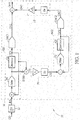
- FIG. 1 is a schematic diagram of a sigma-delta ( ⁇ ) digital-to-analog convertor (DAC) according to an embodiment of the present application.
- the sigma-delta DAC 10 is an oversampling sigma-delta DAC.
- the sigma-delta DAC 10 configured to convert a digital signal OD as an overall analog output signal OAA, comprises an upsampling circuit 12 and a noise shaping circuit 14.
- the upsampling circuit 12 is configured to perform upsampling operation on the digital signal OD and generate a digital input signal ID1.
- the noise shaping circuit 14 comprises modulation units NS1 and NS2, digital-to-analog convertors DAC1 and DAC2, a subtractor SUB1 and filters F3, F4 .
- the modulation unit NS1 coupled to the upsampling circuit 12, is configured to receive the digital input signal ID1 and generate a digital output signal OD1.
- the modulation unit NS1 comprises a filter F1 and a quantizer Q1.
- the quantizer Q1 is coupled to the filter F1, and the filter F1 has a transfer function H1.
- the subtractor SUB1, coupled to an input terminal and an output terminal of the quantizer Q1, is configured to generate a quantization noise e1 corresponding to the quantizer Q1.
- the modulation unit NS2 coupled to the subtractor SUB1, is configured to generate a digital output signal OD2 according to a digital input signal ID2, where the digital input signal ID2 is related to the quantization noise e1.
- the modulation unit NS2 comprises a filter F2 and a quantizer Q2.
- the quantizer Q2 is coupled to the filter F2, and the filter F2 has a transfer function H2.
- the noise shaping circuit 14 generates the overall analog output signal OAA according to the digital output signal OD1 and the digital output signal OD2.
- a first filter order of the filter F1 may be larger than or equal to a second filter order of the filter F2.
- the filter F1 may be a second order filter.
- the filter F2 may be a first order filter.
- the filter F3 is an analog filter with a direct current (DC) gain (1/G) and a transfer function Ha, where a value of the transfer function Ha corresponding to a DC frequency is 1.
- the filter F3, coupled to the modulation unit NS2, is configured to generate the filter result OA3.
- the noise shaping circuit 14 generates the overall analog output signal OAA according to the digital output signal OD1 and the filter result OA3.
- the DC gain (1/G) of the filter F3 is less than 1.
- the filter F3 is a high pass filter (HPF) with a corner frequency Fc. In other words, the filter F3 would filter out signal of which frequency is less than the corner frequency Fc, and deliver signal of which frequency is larger than the corner frequency Fc.
- the filter F4 is a digital filter with an inverting DC gain (-G) and a transfer function Hc.
- the filter F4, coupled to the subtractor SUB1, is configured to perform filtering operation on the quantization noise e1, to generate the digital input signal ID2.
- the filtering operation the filter F4 performs on the quantization noise e1 is equivalent to multiply the quantization noise e1 by the inverting gain (-G) and the transfer function Hc.
- the transfer function Hc is related to the transfer function H1 of the filter F1 and the transfer function Ha of the filter F3.
- the transfer function Hc is related to a reciprocal of the transfer function Ha.
- the digital-to-analog convertors DAC1 and DAC2 are coupled to the modulation units NS1 and NS2, configured to convert the digital output signals OD1 and OD2 as analog output signals OA1 and OA2, respectively.
- the filter F3, coupled to the digital-to-analog convertor DAC2, is configured to perform filtering operation on the analog output signal OA2.
- the filtering operation the filter F3 performs on the analog output signal OA2 is equivalent to multiply the analog output signal OA2 by the DC gain (1/G) and the transfer function Ha, to generate the filter result OA3.
- the noise shaping circuit 14 outputs the overall analog output signal OAA as a summation of the analog output signal OA1 and the filter result OA3.
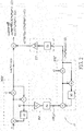
- FIG. 2 is a schematic diagram of equivalent circuit model of another noise shaping circuit 24 according to an embodiment of the present application.
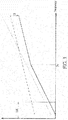
- FIG. 3 is a schematic diagram of shaped noise spectrum.
- the noise shaping circuit 24 comprises modulation units NS1" and NS2", and filters F3" and F4".
- s represents the digital input signal ID1
- e1 represents the quantization noise brought by the quantizer Q1
- e2 represents the quantization noise brought by the quantizer Q2.
- a dashed line represents a noise spectrum after a first order shaping
- a dotted line represents a noise spectrum after a second order shaping
- a solid line represents a noise spectrum of the noise shaped by the noise shaping circuit 24.
- effect caused by the digital-to-analog convertor DAC1 and DAC2 on the noise shaping circuit 14 is ignored in the following description.
- the modulation unit NS1" performs noise shaping on the quantization noise e1 after receiving the digital input signal ID1(corresponding to the signal s).
- the signal outputted by the modulation unit NS1" may be represented as s+e1*(1-H1).
- the filter F4" performs filtering operation on the quantization noise e1.
- the signal outputted by the filter F4" may be represented as G ⁇ Hc ⁇ e1.
- the modulation unit NS2" receives the output signal G ⁇ Hc ⁇ e1 outputted by the filter F4" and performs noise shaping on the quantization noise e2.
- the signal outputted by the modulation unit NS2" may be represented as -G ⁇ Hc ⁇ e1 + e2 ⁇ (1-H2).
- the signal component related to the quantization noise is (1/G)e2 ⁇ Ha ⁇ H2, where the filter F2" may be a first order filter.
- the filter F3" may be a first order high pass filter within the corner frequency Fc. In other words, when frequency is less than the corner frequency Fc, the transfer function Ha is approximately in a first order attenuation; when frequency is larger than the corner frequency Fc, the transfer function Ha is 1.
- the filter F2 when frequency is less than the corner frequency Fc, the filter F2 is a first order filter and the transfer function Ha would apply a first order attenuation on the signal e2 ⁇ H2. Thus, the noise shaping circuit 24 would perform a second order noise shaping on the quantization noise.
- the transfer function Ha when the frequency is larger than the corner frequency Fc, the transfer function Ha is 1 and the filter F2 is still a first order filter. Thus, the noise shaping circuit 24 would perform a first order noise shaping on the quantization noise.
- the noise shaping circuit 24 utilizes the inverting DC gain (-G) of the filter F4 to replace the quantization noise e1 brought by the modulation unit NS1" (i.e., e1 ⁇ (1-H1)) with the quantization noise e2 brought by the modulation unit NS2" (i.e., (1/G)e2 ⁇ Ha ⁇ (1-H2)). Since the quantization noise e2 is processed by the filters F2" and F3" via the transfer functions H2 and Ha, the shaped noise spectrum would be the spectrum illustrated as the solid line in FIG. 3 .
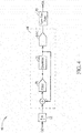
- FIG. 4 is a schematic diagram of an oversampling sigma-delta DAC 40 in the art.
- the oversampling sigma-delta DAC 40 comprises the noise shaping circuit 44, and the noise shaping circuit 44 comprises a filter F.
- the filter F is a second order filter
- the noise spectrum shaped by the noise shaping circuit 44 is the dotted line in FIG. 3 and a slope of the noise spectrum is larger.
- Advantage of the filter F being the second order filter is that the noise energy is low within a signal band SB, but disadvantage thereof is that the noise energy is too large at high frequency.
- the filter F is a first order filter
- the noise spectrum shaped by the noise shaping circuit 44 is the dashed line in FIG. 3 and a slope of the noise spectrum is smaller.
- Advantage of the filter F being the first order filter is that the noise energy is lower at high frequency, but disadvantage thereof is that the noise energy is larger within the signal band SB.
- the noise spectrum shaped by the noise shaping circuit 24 has the property of the second order noise shaping within the signal band SB (i.e., lower noise energy within the signal band SB), and also has the property of the first order noise shaping outside the signal band SB or even at high frequency, (i.e., lower noise energy at high frequency).
- the noise shaping circuit 24 may own advantages of both the first order noise shaping and the second order noise shaping, which means that the noise spectrum shaped by the noise shaping circuit 24 has low noise energy both within the signal band SB and at high frequency.
- the filter F3 has the DC gain (1/G) and the DC gain (1/G) is less than 1.
- FIG. 5 is a schematic diagram of a sigma-delta DAC 50 according to an embodiment of the present application.
- the sigma-delta DAC 50 comprises a noise shaping circuit 54
- the noise shaping circuit 54 comprises modulation units NS1' and NS2', and filters F3' and F4'.
- the modulation units NS1' and NS2' and the filters F3' and F4' are configured to realize the modulation units NS1 and NS2 and the filters F3 and F4 of the noise shaping circuit 14 in FIG. 1 , respectively.
- the filter F3' is an analog high pass first order filter, which comprises the operational amplifier OP, a capacitor C, a resistor R and a resistor G*R, where a resistance of the resistor G*R is G times a resistance of the resistor R.
- the resistor R is coupled between a negative input terminal (denoted by "-") and an output terminal of the operational amplifier OP.
- the resistor R and the resistor G*R are coupled between the negative input terminal of the operational amplifier OP and the output terminal of the digital-to-analog convertor DAC2.
- the DC gain of the filter F3' is (1/G), such that the noise spectrum shaped by the noise shaping circuit 54 is able to be shifted downward by the factor G.
- the corner frequency Fc of the filter F3' may be represented as 1/(2 ⁇ GRC).
- the noise shaping circuit 24 utilizes the subtractor to capture the quantization noise e1 corresponding to the quantizer Q1; utilizes the filters F3" and F4" to recover the signal component related to the quantization noise e1 within the signal outputted by the modulation unit NS2" as e1 ⁇ (1-H1), so as to cancel the signal component related to the quantization noise e1 within the signal outputted by the modulation unit NS1"; utilizes the filters F2" and F3" to shape the quantization noise e2 to be the spectrum illustrated as the solid line in FIG. 3 ; and utilizes the resistor G*R to lower the noise spectrum, increase signal-to-noise ratio (SNR), and reduce circuit area.
- SNR signal-to-noise ratio
- the filter F1 is not limited to be a second order filter.
- the filter F1 may be a filter with even higher order, which is also within the scope of the present application.
- the present application utilizes the two modulation units and the analog high pass filter to form the shaped noise spectrum with various slopes, which incorporates properties of both low order noise shaped spectrum and high order noise shaped spectrum.
- the present application has advantage of being able to lower the noise spectrum, increase SNR and reduce circuit area.
Landscapes
- Engineering & Computer Science (AREA)
- Theoretical Computer Science (AREA)
- Compression, Expansion, Code Conversion, And Decoders (AREA)
- Analogue/Digital Conversion (AREA)
Applications Claiming Priority (1)
| Application Number | Priority Date | Filing Date | Title |
|---|---|---|---|
| PCT/CN2017/088388 WO2018227456A1 (zh) | 2017-06-15 | 2017-06-15 | 噪声整形电路与三角积分数模转换器 |
Publications (2)
| Publication Number | Publication Date |
|---|---|
| EP3447922A4 EP3447922A4 (de) | 2019-02-27 |
| EP3447922A1 true EP3447922A1 (de) | 2019-02-27 |
Family
ID=63556826
Family Applications (1)
| Application Number | Title | Priority Date | Filing Date |
|---|---|---|---|
| EP17800989.0A Ceased EP3447922A1 (de) | 2017-06-15 | 2017-06-15 | Rauschformerschaltung und sigma-delta-digital-analog-wandler |
Country Status (5)
| Country | Link |
|---|---|
| US (1) | US10084474B1 (de) |
| EP (1) | EP3447922A1 (de) |
| KR (1) | KR102096294B1 (de) |
| CN (1) | CN109690955A (de) |
| WO (1) | WO2018227456A1 (de) |
Families Citing this family (6)
| Publication number | Priority date | Publication date | Assignee | Title |
|---|---|---|---|---|
| US10341148B2 (en) * | 2017-08-25 | 2019-07-02 | Mediatek Inc. | Sigma-delta modulator and associated system improving spectrum efficiency of wired interconnection |
| US10979030B2 (en) * | 2017-08-25 | 2021-04-13 | Mediatek Inc. | System improving signal handling |
| DE102021100771A1 (de) | 2021-01-15 | 2022-07-21 | Universität Stuttgart, Körperschaft Des Öffentlichen Rechts | Mischsignal-Schaltungsanordnung und Verfahren zur effizienten Pulsformung digitaler Signale |
| US12126363B2 (en) * | 2022-07-29 | 2024-10-22 | Cisco Technology, Inc. | Error cancellation delta-sigma DAC with an inverting amplifier-based filter |
| CN116593764B (zh) * | 2023-03-29 | 2024-06-25 | 浙江朗德电子科技有限公司 | 高精度自标定电流传感器模块及其标定方法 |
| US12525984B2 (en) * | 2024-02-14 | 2026-01-13 | Qualcomm Incorporated | Noise-shaping ADC with overload recovery |
Family Cites Families (22)
| Publication number | Priority date | Publication date | Assignee | Title |
|---|---|---|---|---|
| DE3642168A1 (de) * | 1986-12-10 | 1988-06-16 | Philips Patentverwaltung | Digitale schaltungsanordnung zur verringerung des quantisierungsrauschens |
| US4862169A (en) * | 1988-03-25 | 1989-08-29 | Motorola, Inc. | Oversampled A/D converter using filtered, cascaded noise shaping modulators |
| JPH07118652B2 (ja) * | 1990-10-12 | 1995-12-18 | ヤマハ株式会社 | Da変換装置 |
| GB9109637D0 (en) * | 1991-05-03 | 1991-06-26 | Marconi Gec Ltd | Analogue-to-digital and digital-to-analogue converters |
| US5369403A (en) * | 1992-09-01 | 1994-11-29 | The State Of Oregon Acting By And Through The State Board Of Higher Education On Behalf Of Oregon State University | Dual quantization oversampling digital-to-analog converter |
| US5870048A (en) * | 1997-08-13 | 1999-02-09 | National Science Council | Oversampling sigma-delta modulator |
| US6373417B1 (en) * | 1999-02-23 | 2002-04-16 | Cirrus Logic, Inc. | Digital to analog converter using level and timing control signals to cancel noise |
| JP2002344321A (ja) * | 2001-05-16 | 2002-11-29 | Pioneer Electronic Corp | デルタシグマ型ad変換器 |
| EP1335494A1 (de) * | 2001-12-19 | 2003-08-13 | Siemens Aktiengesellschaft | Sigma-Delta-Wandler mit Rauschunterdrückung |
| JP3718706B2 (ja) * | 2003-10-28 | 2005-11-24 | 松下電器産業株式会社 | デルタ・シグマ変調装置 |
| WO2005074139A2 (en) * | 2004-01-28 | 2005-08-11 | Koninklijke Philips Electronics N.V. | A da-converter system and a method for converting a multi-bit digital signal to an analog signal |
| GB0611639D0 (en) * | 2006-06-12 | 2006-07-19 | Global Silicon Ltd | A sigma-delta modulator |
| US7903015B1 (en) * | 2009-08-24 | 2011-03-08 | Texas Instruments Incorporated | Cascaded DAC architecture with pulse width modulation |
| US8031096B2 (en) * | 2010-02-18 | 2011-10-04 | Taiwan Semiconductor Manufacturing Company, Ltd. | High resolution delta-sigma digital-to-analog converter |
| US8228221B2 (en) * | 2010-09-28 | 2012-07-24 | Taiwan Semiconductor Manufacturing Co., Ltd. | Method and apparatus for calibrating sigma-delta modulator |
| US8284085B2 (en) * | 2010-10-06 | 2012-10-09 | Texas Instruments Incorporated | Pipelined continuous-time sigma delta modulator |
| US8325074B2 (en) * | 2011-03-22 | 2012-12-04 | Taiwan Semiconductor Manufacturing Co., Ltd. | Method and circuit for continuous-time delta-sigma DAC with reduced noise |
| CN105009459B (zh) * | 2012-12-21 | 2017-08-11 | 特利丹达尔萨公司 | Σ‑δ模数转换器 |
| US8952837B2 (en) * | 2013-02-28 | 2015-02-10 | Broadcom Corporation | Multi-rate sigma delta digital-to-analog converter |
| KR101485467B1 (ko) * | 2013-05-24 | 2015-01-22 | 네오피델리티 주식회사 | 시그마-델타 변조부를 포함하는 양자화 장치, 이를 포함하는 adc 및 이를 이용한 양자화 방법 |
| US9166615B2 (en) * | 2013-12-13 | 2015-10-20 | Taiwan Semiconductor Manufacturing Co., Ltd. | System and method for cascaded PWM digital-to-analog converter with hybrid DAC interface |
| CN204559547U (zh) * | 2015-06-04 | 2015-08-12 | 福州大学 | 一种高二阶级联结构Sigma-Delta调制器系统 |
-
2017
- 2017-06-15 KR KR1020177036107A patent/KR102096294B1/ko active Active
- 2017-06-15 CN CN201780000513.4A patent/CN109690955A/zh active Pending
- 2017-06-15 WO PCT/CN2017/088388 patent/WO2018227456A1/zh not_active Ceased
- 2017-06-15 EP EP17800989.0A patent/EP3447922A1/de not_active Ceased
- 2017-11-26 US US15/822,190 patent/US10084474B1/en active Active
Also Published As
| Publication number | Publication date |
|---|---|
| EP3447922A4 (de) | 2019-02-27 |
| KR102096294B1 (ko) | 2020-04-03 |
| KR20190010397A (ko) | 2019-01-30 |
| US10084474B1 (en) | 2018-09-25 |
| CN109690955A (zh) | 2019-04-26 |
| WO2018227456A1 (zh) | 2018-12-20 |
Similar Documents
| Publication | Publication Date | Title |
|---|---|---|
| US10084474B1 (en) | Noise shaping circuit and sigma-delta digital-to-analog converter | |
| US8988260B2 (en) | Method and circuit for continuous-time delta-sigma DAC with reduced noise | |
| CN107852164B (zh) | 抑制前馈δς转换器中的信号传递函数峰化 | |
| JP4897825B2 (ja) | 最適内蔵フィルタ関数を有するフィードフォワードシグマ−デルタad変換器 | |
| JP4890503B2 (ja) | デルタシグマ変調器 | |
| US8248285B2 (en) | Multi-bit sigma-delta modulator with reduced number of bits in feedback path | |
| US10491237B1 (en) | Continuous-time delta-sigma modulator | |
| US11451239B2 (en) | Power reduction and performance enhancement techniques for delta sigma modulator | |
| KR102499229B1 (ko) | 고-선형성 시그마-델타 컨버터 | |
| EP4113847B1 (de) | Sigma-delta-modulator und verfahren dafür | |
| US20110175761A1 (en) | Delta sigma analogue to digital converter | |
| KR20150084267A (ko) | 델타-시그마 변조기 | |
| CN104639168A (zh) | Sigma-Delta型模数转换器模拟前端电路 | |
| US9100041B1 (en) | Flash converter capacitance reduction method | |
| US7352311B2 (en) | Continuous time noise shaping analog-to-digital converter | |
| US6956513B1 (en) | Error feedback structure for delta-sigma modulators with improved stability | |
| US9172494B2 (en) | Modulator device | |
| US7675446B2 (en) | Filter applied in sigma-delta modulator and filtering method thereof | |
| CN116054835A (zh) | 一种用于sigma-delta ADC的参考电压发生器的斩波时序控制方法及系统 | |
| CN204316489U (zh) | 低噪声过采样模数转换器 | |
| JP2008530890A (ja) | Ad変換装置 | |
| US10892770B2 (en) | Noise shaping in a digital-to-analog convertor | |
| Silva-Martinez et al. | Blocker and jitter tolerant wideband ΣΔ modulators | |
| Balagopal et al. | A 1 GS/s, 31 MHz BW, 76.3 dB dynamic range, 34 mW CT-ΔΣ ADC with 1.5 cycle quantizer delay and improved STF | |
| JPH04101517A (ja) | Σ△変調形ad変換器 |
Legal Events
| Date | Code | Title | Description |
|---|---|---|---|
| STAA | Information on the status of an ep patent application or granted ep patent |
Free format text: STATUS: UNKNOWN |
|
| STAA | Information on the status of an ep patent application or granted ep patent |
Free format text: STATUS: THE INTERNATIONAL PUBLICATION HAS BEEN MADE |
|
| PUAI | Public reference made under article 153(3) epc to a published international application that has entered the european phase |
Free format text: ORIGINAL CODE: 0009012 |
|
| STAA | Information on the status of an ep patent application or granted ep patent |
Free format text: STATUS: REQUEST FOR EXAMINATION WAS MADE |
|
| 17P | Request for examination filed |
Effective date: 20171129 |
|
| A4 | Supplementary search report drawn up and despatched |
Effective date: 20181008 |
|
| AK | Designated contracting states |
Kind code of ref document: A1 Designated state(s): AL AT BE BG CH CY CZ DE DK EE ES FI FR GB GR HR HU IE IS IT LI LT LU LV MC MK MT NL NO PL PT RO RS SE SI SK SM TR |
|
| AX | Request for extension of the european patent |
Extension state: BA ME |
|
| DAV | Request for validation of the european patent (deleted) | ||
| DAX | Request for extension of the european patent (deleted) | ||
| STAA | Information on the status of an ep patent application or granted ep patent |
Free format text: STATUS: EXAMINATION IS IN PROGRESS |
|
| 17Q | First examination report despatched |
Effective date: 20210318 |
|
| REG | Reference to a national code |
Ref country code: DE Ref legal event code: R003 |
|
| STAA | Information on the status of an ep patent application or granted ep patent |
Free format text: STATUS: THE APPLICATION HAS BEEN REFUSED |
|
| 18R | Application refused |
Effective date: 20230412 |