EP3449266B1 - Spannungsdetektor und spannungsdetektorsystem - Google Patents
Spannungsdetektor und spannungsdetektorsystem Download PDFInfo
- Publication number
- EP3449266B1 EP3449266B1 EP17724605.5A EP17724605A EP3449266B1 EP 3449266 B1 EP3449266 B1 EP 3449266B1 EP 17724605 A EP17724605 A EP 17724605A EP 3449266 B1 EP3449266 B1 EP 3449266B1
- Authority
- EP
- European Patent Office
- Prior art keywords
- voltage
- input
- threshold
- voltage detector
- signal
- Prior art date
- Legal status (The legal status is an assumption and is not a legal conclusion. Google has not performed a legal analysis and makes no representation as to the accuracy of the status listed.)
- Active
Links
Images





Classifications
-
- G—PHYSICS
- G05—CONTROLLING; REGULATING
- G05F—SYSTEMS FOR REGULATING ELECTRIC OR MAGNETIC VARIABLES
- G05F3/00—Non-retroactive systems for regulating electric variables by using an uncontrolled element, or an uncontrolled combination of elements, such element or such combination having self-regulating properties
- G05F3/02—Regulating voltage or current
- G05F3/08—Regulating voltage or current wherein the variable is DC
- G05F3/10—Regulating voltage or current wherein the variable is DC using uncontrolled devices with non-linear characteristics
-
- G—PHYSICS
- G01—MEASURING; TESTING
- G01R—MEASURING ELECTRIC VARIABLES; MEASURING MAGNETIC VARIABLES
- G01R15/00—Details of measuring arrangements of the types provided for in groups G01R17/00 - G01R29/00, G01R33/00 - G01R33/26 or G01R35/00
- G01R15/04—Voltage dividers
-
- G—PHYSICS
- G01—MEASURING; TESTING
- G01R—MEASURING ELECTRIC VARIABLES; MEASURING MAGNETIC VARIABLES
- G01R19/00—Arrangements for measuring currents or voltages or for indicating presence or sign thereof
- G01R19/165—Indicating that current or voltage is either above or below a predetermined value or within or outside a predetermined range of values
- G01R19/16504—Indicating that current or voltage is either above or below a predetermined value or within or outside a predetermined range of values characterised by the components employed
- G01R19/16519—Indicating that current or voltage is either above or below a predetermined value or within or outside a predetermined range of values characterised by the components employed using FET's
-
- G—PHYSICS
- G01—MEASURING; TESTING
- G01R—MEASURING ELECTRIC VARIABLES; MEASURING MAGNETIC VARIABLES
- G01R19/00—Arrangements for measuring currents or voltages or for indicating presence or sign thereof
- G01R19/165—Indicating that current or voltage is either above or below a predetermined value or within or outside a predetermined range of values
- G01R19/16533—Indicating that current or voltage is either above or below a predetermined value or within or outside a predetermined range of values characterised by the application
- G01R19/16538—Indicating that current or voltage is either above or below a predetermined value or within or outside a predetermined range of values characterised by the application in AC or DC supplies
-
- G—PHYSICS
- G01—MEASURING; TESTING
- G01R—MEASURING ELECTRIC VARIABLES; MEASURING MAGNETIC VARIABLES
- G01R19/00—Arrangements for measuring currents or voltages or for indicating presence or sign thereof
- G01R19/165—Indicating that current or voltage is either above or below a predetermined value or within or outside a predetermined range of values
- G01R19/16566—Circuits and arrangements for comparing voltage or current with one or several thresholds and for indicating the result not covered by subgroups G01R19/16504, G01R19/16528, G01R19/16533
- G01R19/16576—Circuits and arrangements for comparing voltage or current with one or several thresholds and for indicating the result not covered by subgroups G01R19/16504, G01R19/16528, G01R19/16533 comparing DC or AC voltage with one threshold
-
- G—PHYSICS
- G05—CONTROLLING; REGULATING
- G05F—SYSTEMS FOR REGULATING ELECTRIC OR MAGNETIC VARIABLES
- G05F3/00—Non-retroactive systems for regulating electric variables by using an uncontrolled element, or an uncontrolled combination of elements, such element or such combination having self-regulating properties
- G05F3/02—Regulating voltage or current
- G05F3/08—Regulating voltage or current wherein the variable is DC
- G05F3/10—Regulating voltage or current wherein the variable is DC using uncontrolled devices with non-linear characteristics
- G05F3/16—Regulating voltage or current wherein the variable is DC using uncontrolled devices with non-linear characteristics being semiconductor devices
- G05F3/20—Regulating voltage or current wherein the variable is DC using uncontrolled devices with non-linear characteristics being semiconductor devices using diode- transistor combinations
- G05F3/24—Regulating voltage or current wherein the variable is DC using uncontrolled devices with non-linear characteristics being semiconductor devices using diode- transistor combinations wherein the transistors are of the field-effect type only
-
- H—ELECTRICITY
- H03—ELECTRONIC CIRCUITRY
- H03K—PULSE TECHNIQUE
- H03K17/00—Electronic switching or gating, i.e. not by contact-making and –breaking
- H03K17/22—Modifications for ensuring a predetermined initial state when the supply voltage has been applied
- H03K17/223—Modifications for ensuring a predetermined initial state when the supply voltage has been applied in field-effect transistor switches
Definitions
- the present application relates to a voltage detector and a voltage detector system.
- Sensors such as those used in medical devices can be powered by wireless power transfer or energy harvesting sources.
- these sources provide intermittent power due to the body's movement. For example, if the wearer of the device rests in a position such that a power receiving antenna is poorly oriented relative to the transmitter, then an input power lull occurs. This problem of intermittency occurs with the majority of energy generation and wireless power transfer techniques, and is only exacerbated when some of the system is situated on a moving body.
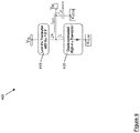
- Figure 1 provides a schematic illustration of a sensor system that may be powered by intermittent sources.
- the intermittent source feeds an input rail V IN .
- a power management circuit converts V IN into a useful stable internal rail voltage V DD for the sensor sub-systems.
- the power management circuit requires power for its own internal control circuits, which is supplied from the V DD rail. In order to stop this quiescent power from unnecessarily draining power from the V DD rail, the power management is powered off during input power lulls.
- a voltage detector the device under consideration here, senses the input voltage V IN , and power-gates the power management circuit via a PMOS transistor, which is switched by the voltage detector's open-drain output Enable .
- Three-terminal voltage detectors are used that do not require connection to a supply rail, and therefore, in principle provide always-awake input monitoring, even when the rest of the sensor system is powered off.
- the voltage detector could be used to switch on a power supply, for example from a battery, thus minimising use of stored power to when there is a detection signal.
- Figure 2 shows the operation of a commercially available voltage detector being used in the circuit of Figure 1 .
- Figure 2 shows the source voltage V IN when the source is unloaded (dashed line), and also when loaded by the voltage detector (solid line).
- the quiescent current I IN increases sharply, dragging the input voltage down, thus switching the detector off again.
- the quiescent input current drops and the process begins again, resulting in a pulsing output V OD rather than an output pulse that lasts the duration of the incoming power, as required for the power-gating of sensor sub-systems.
- the source voltage V IN has been affected in such a way that the supply to the power management circuit shown in Figure 1 is significantly reduced.
- POR Power-On-Reset circuit
- Figure 3 illustrates the operation of a basic POR pulse generator circuit. However, the output is a short reset-pulse, which does not provide information on the duration of the incoming source power.
- Figure 4 shows the desired behaviour of an ideal voltage detector, where the incoming voltage is preserved, the quiescent current is zero most of the time, and the output lasts the duration of the incoming power.
- a voltage detector consists of a comparator and a band-gap reference to determine the input condition.
- the quiescent current of this circuit is 180 nA, mostly due to continuous flow of bias current through reference-voltage generating circuitry and the comparator.
- the voltage detection threshold of this circuit is 2.1V and the maximum operating voltage is 4V. Additional protection circuits could be used to protect the circuit from potentially damaging over voltage conditions, but by clamping the input voltage at 4V, a significant percentage of the source power would be lost.
- a monitoring circuit consuming sub-nA current has also been proposed (Toshishige Shimamura, Mamoru Ugajin, Kenji Suzuki, Kazuyoshi Ono,Norio Sato, Kei Kuwabara, Hiroki Morimura, Shin'ichiro Mutoh: "Nano-Watt Power Management and Vibration Sensing on a Dust-Size Batteryless Sensor Node for Ambient Intelligence”). It operates without the need for a bandgap voltage reference for low power, but triggers only at a high input voltage.
- a battery supervisor circuit consuming 635 pW at 3.6 V is reported in " A 635pW Battery Voltage Supervisory Circuit for Miniature Sensor Nodes" by I. Lee, S. Bang, Y. Lee, Y. Kim, G. Kim, D. Sylvester, and D. Blaauw .
- This circuit achieves low power consumption through a 57 pA voltage reference and a low power comparator.
- the detection threshold is 3.6 V, which is too high for many applications.
- US20110095789A1 discloses a circuit for detecting an input voltage including a voltage-to-current converter and a current comparator.
- the voltage-to-current converter is operable for generating a monitoring current that varies in accordance with the input voltage.
- the current comparator coupled to the voltage-to-current converter is operable for comparing the monitoring current to a threshold current proportional to the temperature of the circuit, and for generating a detection signal indicating a condition of the input voltage based on a result of the comparison.
- WO2015072522A1 discloses a voltage detector for detecting whether an input voltage is no lower than a predetermined threshold voltage, including a reference voltage generator configured to generate a reference voltage, and a comparator configured to receive the input voltage and the reference voltage and to detect whether the input voltage is no lower than the threshold voltage that is determined by the reference voltage.
- the reference voltage generator includes a first write MOS transistor, a second write MOS transistor, a first output MOS transistor and a second output MOS transistor each including a control gate and a floating gate.
- a voltage detector comprising: a first voltage reference generator for generating a first voltage reference signal; a second voltage reference generator for generating a second voltage reference signal, wherein the first voltage reference signal is higher than the second voltage reference signal; a third voltage reference generator for generating a third voltage reference signal, wherein the third voltage reference generator is configured to output the third voltage reference signal to the first and second voltage reference generators; a trigger, powered by an input signal to the voltage detector, and having an input for receiving either the first or second voltage reference signal and an output for generating a detection signal; and a switch for selectively connecting the input of the trigger to the first or second voltage reference signal, wherein: the switch is operative to connect the input of the trigger to the first voltage reference signal when the detection signal output by the trigger is low and is operative to connect the input of the trigger to the second voltage reference signal when the detection signal output by the trigger is high; the first and second voltage reference generators of the voltage detector each comprise a first transistor, arranged to have a zero
- the first and second voltage reference generators of the voltage detector each comprise a first transistor and a second transistor connected in series between the input signal and a common reference, wherein the first transistor has a different gate threshold than the second transistor.
- the trigger may comprise a PMOS transistor and an NMOS transistor connected so as to form an inverter.
- the first and second reference voltage signals produced by the first and second voltage reference circuits may be low enough to ensure that the inverter is in subthreshold mode when it switches.
- the common reference may be ground.
- the voltage detector comprises a third voltage reference generator for generating a third voltage reference signal, wherein the third voltage reference generator is configured to output the third voltage reference signal to the first and second voltage reference generators.
- a voltage detector system for monitoring an input signal and outputting a detection signal when the voltage of the input signal meets a threshold
- the voltage detector system comprising: a first voltage detector having an input for receiving the input signal and an output for outputting a detection signal, wherein the first voltage detector is configured to output the detection signal when the voltage of the input signal meets a first rising input voltage threshold; a second voltage detector having an input for receiving the input signal and an output for outputting a detection signal, wherein the second voltage detector is configured to output the detection signal when the voltage of the input signal meets a second rising input voltage threshold which is higher than the first threshold, wherein the first and/or second voltage detector is according to the first aspect of the invention, and the output of the second voltage detector controls a connection between the input signal and the input of the first voltage detector such that when the voltage of the input signal meets the second rising input voltage threshold the connection between the input signal and the input of the first voltage detector is restricted or disconnected.
- the voltage detector system may further comprise: a third voltage detector having an input for receiving the input signal and an output for outputting a detection signal, wherein the third voltage detector is configured to output a detection signal when the voltage of the input signal meets a third rising input voltage threshold which is higher than both the first threshold and the second threshold, wherein the output of the third voltage detector controls a connection between the input signal and the input of the second voltage detector such that when the voltage of the input signal meets the third rising input voltage threshold the connection between the input signal and the input of the second voltage detector is restricted or disconnected.
- a third voltage detector having an input for receiving the input signal and an output for outputting a detection signal
- the third voltage detector is configured to output a detection signal when the voltage of the input signal meets a third rising input voltage threshold which is higher than both the first threshold and the second threshold
- the output of the third voltage detector controls a connection between the input signal and the input of the second voltage detector such that when the voltage of the input signal meets the third rising input voltage threshold the connection between the input signal and the input of the second voltage
- the third voltage detector may be according to the first aspect of the invention.
- the first voltage detector may be configured to cease outputting a detection signal when the voltage of the input signal meets a first falling input voltage threshold, wherein the first falling input voltage threshold is lower than the first rising input voltage threshold.
- the second voltage detector may be configured to cease outputting a detection signal when the voltage of the input signal meets a second falling input voltage threshold, wherein the second falling input voltage threshold is lower than the second rising input voltage threshold.
- the third voltage detector may be configured to cease outputting a detection signal when the voltage of the input signal meets a third falling input voltage threshold, wherein the third falling input voltage threshold is lower than the third rising input voltage threshold.
- the voltage detection system may further comprise an open drain output stage, the output stage comprising a plurality of MOSFET devices, each MOSFET device having: a gate terminal connected to an output of a respective one of the voltage detectors; a source terminal connected to the common reference; and a drain terminal connected to an output terminal of the output stage.
- a gate threshold of each MOSFET device may be lower than the rising input threshold and the falling input threshold of the respective voltage detector to which the MOSFET device is connected.
- Figure 5 illustrates a voltage detection system which combines all the desired properties of voltage detectors, namely high maximum input voltage, a low voltage detection threshold and low quiescent power consumption.
- the system shown generally at 100 in Figure 1 , includes a power gating stage 120, a voltage detection stage 140 and an output stage 160.
- the voltage detection stage 140 includes a first voltage detector 142 which is configured to detect input voltages in a high voltage range (e.g. in the range 2.8 volts to 20 volts), a second voltage detector 144 which is configured to detect input voltages in a medium voltage range (e.g. 0.6 volts to 2.8 volts) and a third voltage detector 146 which is configured to detect input voltages in a low voltage range (e.g. 0.45 volts to 0.6 volts).
- This arrangement of three voltage detectors ensures that the voltage detection system 100 is able to operate in a wide input voltage range, therefore facilitating the capture of energy from pulses with a wide power range.
- the power gating stage 120 is configured to prevent potentially damaging input voltages from reaching the second and third voltage detectors 144, 146, and is arranged such that the first voltage detector 142 gates the second and third voltage detectors 144, 146 and the second voltage detector 144 gates the third voltage detector 146.
- the voltage input V IN of the system 100 is connected to an input V IN(H) of the first voltage detector 142.
- An output V OUT(H) of the first voltage detector 142 is connected to the gate terminal of a first P-channel MOSFET 122.
- the source terminal of the first P-channel MOSFET is connected to the voltage input V IN and the drain terminal of the first P-channel MOSFET 122 is connected to an input V IN(M) of the second voltage detector 144, and, via a second P-channel MOSFET 124, to an input V IN(L) of the third voltage detector 146.
- the first voltage detector 142 detects an input voltage in the high voltage range, its output V OUT(H) goes high, causing the first P-channel MOSFET 122 to switch off, thereby restricting or preventing the input voltage from reaching the second voltage detector 144 or the third voltage detector 146.
- the gate terminal of the second P-channel MOSFET 124 is connected to an output V OUT(m) of the second voltage detector 144, such that when the second voltage detector 144 detects an input voltage in the medium voltage range, its output V OUT(M) goes high, causing the second P-channel MOSFET 124 to switch off, thereby restricting or preventing the input voltage from reaching the third voltage detector 146.
- the output stage 160 of the voltage detection system 100 includes (in the illustrated example) first, second and third N-channel MOSFETS 162, 164, 166.
- the gate terminal of the first N-channel MOSFET 162 is connected to the output V OUT(H) of the first voltage detector 142, whilst the gate terminal of the second N-channel MOSFET 164 is connected to the output V OUT(M) of the second voltage detector 144 and the output of the third N-channel MOSFET 166 is connected to the output V OUT(L) of the third voltage detector 146.
- the drain terminals of the first, second and third N-channel MOSFETs 162, 164, 166 are all connected to an open-drain output terminal V OD of the output stage 160, whilst the source terminals of the first, second and third N-channel MOSFETs 162, 164, 166 are all connected to ground. Accordingly, if any one of the first, second or third voltage detectors 142, 144, 146 is triggered, the open drain output V OD of the output stage 160 will be activated.
- FIG. 6 is a timing diagram illustrating the operation of the circuit of Figure 5 .
- the input voltage V IN is shown as a trapezoidal pulse. As the rising edge of this pulse reaches the voltage detection threshold of the third (low voltage range) voltage detector 146, the third voltage detector 146 turns the third N-channel MOSFET 166 on, activating the system's output V OD .
- the second voltage detector 144 switches on the second N-channel MOSFET 164, and power-gates off the third voltage detector 146, thus protecting it from a further rise in V IN , and causing the third N-channel MOSFET 166 to be switched off.
- the first N-channel MOSFET 162 is switched on, and both the second and third voltage detectors 144, 146 are disconnected from the input (or at least the connection restricted), resulting in the turning off of the second N-channel MOSFET 164.
- the first voltage detector 142 remains active until the input voltage drops below its voltage detection threshold, which leads to the second voltage detector 144 being powered on. A further fall in the input voltage activates the third voltage detector 146.
- the thresholds at which the voltage detectors 142, 144, 146 switch on in response to a rising input voltage may be different from (higher than) the thresholds at which the voltage detectors 142, 144, 146 switch off in response to a falling input voltage, in order to provide hysteresis and thus avoid system oscillation.
- the overall result is a continuous activation of the open-drain output V OD for the duration of the input pulse.
- the threshold voltage of each MOSFET device 162, 164, 166 should be lower than the detection thresholds at which the respective voltage detectors 142, 144, 146 switch on in response to a rising input voltage and the thresholds at which the respective voltage detectors 142, 144, 146 switch off in response to a falling input voltage.
- V OUT(H) , V OUT(M) and V OUT(L) of the voltage detectors 142, 144, 146 are at the same potential as their corresponding inputs V IN(H) , V IN(M) and V IN(L) . Since the voltage detector system 100 will interface to other CMOS devices with much lower maximum allowable voltages, V OUT(H) and V OUT(M) cannot be used as the output of the overall system.
- the open drain output stage allows the voltage detector system 100 to output a signal that is usable by, and not damaging to, an external device.
- Figure 6 also illustrates the profile of the total quiescent current I IN of the voltage detector system 100.
- An alternative version of the voltage detector system 100 in which the third voltage detector 144 is disabled draws 1.2pA at 0.2V, around 6pA at 1V and 111pA at 5V. Its total energy consumption at 1V/s and 100V/s transition from 0 to 2.8V of the input voltage is 229pJ and 23pJ respectively.
- Figure 7 is a schematic diagram illustrating a voltage detector for use in the voltage detector system 100 shown in Figure 5 , to form the first, second and/or third voltage detector 142, 144, 146 used in the voltage detector system 100.
- the voltage detector shown generally at 300 in Figure 7 , provides a programmable trigger threshold that is not fixed by the process technology chosen.
- the detection threshold and hysteresis can be set, at the time of circuit design, to a desired value. This is desirable for under-voltage-lockout circuits that activate other circuits in a specific input voltage band.
- the voltage detector 300 has a trigger stage 310 which is powered by the input signal V IN .
- the trigger stage 310 comprises an inverter formed by a transistor pair consisting of a PMOS transistor 312 (labelled MP1 in Figure 7 ) and an NMOS transistor 314 (labelled MN1 in Figure 7 ), followed by two inverter buffer stages 320, 330, which drive an open-drain output switch 340.
- the voltage detector 300 also includes a first ultra-low-power voltage reference circuit 350 and a second ultra-low-power voltage reference circuit 360, which generate, respectively, a fixed higher reference voltage V ref_H and a lower voltage V ref_L .
- the body terminal voltages V ref_BB of the first and second ultra-low-power voltage reference circuits 350, 360 are shown in Figure 7 to be controlled by another voltage reference.
- This other voltage reference may be, for example, a further reference generator block 370 with output V ref_BB .
- two reference generator blocks could be provided, one for each of the first and second ultra-low-power voltage reference circuits 350, 360.
- the V ref_BB inputs to the high and low voltage reference blocks could be provided by nodes internal to these blocks themselves (self-biased blocks). The self-biased version will now be discussed.
- V ref_H and V ref_L are multiplexed by a switch 380 to a single reference input V ref to the gate of the trigger stage 310.
- the switch 380 connects the output of the first ultra-low-power voltage reference circuit 350 (i.e. the higher reference voltage V ref_H ) to the input of the trigger stage 310, whilst when the output signal V OUT of the voltage detector 300 is high, the switch 380 connects the output of the second ultra-low-power voltage reference circuit 360 (i.e. the lower reference voltage V ref_L ) to the input of the trigger stage 310.
- the two reference voltages V ref_H and V ref_L along with the relative sizing of the PMOS and NMOS transistors 312, 314 which make up the trigger stage 310, determine the different rise and fall detection thresholds (V th_rise and V th_fall ) of the voltage detector 300, to provide detection hysteresis.
- the detection (trigger) thresholds are determined by equating the current I trigger through the PMOS transistor 312 and through the NMOS transistor 314, when the input V IN rises to V th_rise and falls to V th_fall (given that the two transistors 312 and 314 operate in subthreshold and in saturation):
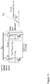
- the operation of the voltage detector 300 is illustrated in Figure 8 .
- the two reference voltages V ref_H and V ref_L and the output V ref_BB of a third reference generator (which, as explained above, may be the further reference generator block 370) rise as V IN increases, and then settle to three different steady-state levels.
- V OUT stays low so that V ref follows V ref_H via the multiplexer 380.
- the PMOS transistor 312 is turned on, and V OUT is thus pulled up to V IN .
- FIG 9 is a schematic representation of a circuit for implementing the first and second voltage reference circuits 350, 360 of Figure 8 .
- the circuit shown generally at 400 consists of two stacked transistors 410, 420 with different gate thresholds V TH .
- a first one 410 of the stacked transistors has a lower V TH and zero gate-source voltage, whilst a second one 420 of the stacked transistors has higher V TH and is configured as a diode-connected transistor.
- the circuit consumes only pico-amperes of current.
- a shortcoming of the circuit 400 is that it is relatively slow to reach a steady-state output during a rising input voltage V IN . For fast rises of V IN , this leads to the reference voltages not having been established by the time the input voltage reaches the desired detection threshold voltage. The circuit 400 therefore triggers too soon.
- the reason for the long start-up time is the circuit's extremely low current that is charging parasitic capacitors.
- the reference generator 370 which provides a reference output V ref_BB , which sets the body bias of the low V TH transistor 410.
- the reference generator 370 speeds up the reference generation, as illustrated in the graph of Figure 10 , thus setting up the detection threshold sooner and allowing higher input voltage gradients.
- Figure 12 is a schematic representation of the circuit of Figure 9 , with an additional body-bias generator, whilst Figure 13 is a schematic diagram showing a body-bias circuit 500 which introduces an additional body-bias generator.
- the body-bias circuit 500 of Figure 13 sets the parameter V ref_BB to be higher than V ref so that V BS becomes positive. This further increases the charging current and makes the current controllable, which in turn speeds up the start-up.
- the V ref_BB value can be customised for different V IN gradients to ensure that V ref has settled before V IN reaches the desired detection threshold. For instance, setting a higher V ref_BB allows for a steeper V IN gradient.
- the transistor sizes of the body-bias generator should be chosen in such a way that V ref_BB has a steeper gradient than V ref when V IN rises. This ensures a positive body-source voltage during the start-up.
- FIG 14 is a schematic representation of a power-gating circuit 120 suitable for use in the voltage detection system 100 of Figure 5 .
- the power-gating transistor 122 (labelled MP2 in Figures 5 and 14 ) should be a medium-gate-oxide (5.5 V breakdown) PMOS transistor because its source-gate voltage can be as high as 2.8 V (corresponding to the threshold of the first voltage detector 142) before its gate-drive signal goes high.
- the power-gating transistor 124 (labelled MP1 in Figures 5 and 22) can be a thin-gate-oxide PMOS transistor because its source-gate voltage does not exceed 0.6 V (corresponding to the threshold of the second voltage detector 144) and its low gate-threshold voltage helps the third (low voltage range) detector 146 start to operate at a low input voltage.
- the input voltage V IN(L) of the third detector 146 will drop after the transistor 122 (MP2) is switched off for protecting this detector.
- the leakage current through the transistor 124 (MP1) when 'OFF') can be sufficiently high so that V IN(L) can continue to rise and follow the input voltage V IN(M) of the second (medium voltage range) detector 144. This may cause overvoltage damage to the third detector 146 especially when V IN(M) has a slow voltage gradient.
- a simple but efficient protection solution is to add a route to ground (or a common reference) for the leakage current.
- this is implemented with a diode-connected NMOS transistor 126 (labelled MN0), which is a thick-gate-oxide (high gate-threshold) transistor.
- MN0 diode-connected NMOS transistor 126
- the second voltage detector 144 output V OUT(M) goes high, which switches off the transistor 124 (MP1) (zero gate-source voltage)
- the two transistors 124 (MP1) and 126 (MN0) are configured as the ultra-low-power two-transistor voltage reference illustrated in Figure 9 .
- V IN(L) clamps V IN(L) to a fixed voltage while consuming pico-amperes current only, and by adjusting the W/L ratios of transistors 124 and 126 (MP1 and MN0), V IN(L) can be set at a safe voltage for the third voltage detector 146.
- transistor 124 (MP1) is switched off and while the third voltage detector 146 is operating normally, transistor 126 (MN0) draws negligible current from the input V IN(L) because its gate-threshold is much higher than V IN(L) and thus this transistor operates in its deep subthreshold region.
- the voltage detector system described herein combines ultra-low power consumption, low detection threshold and wide operating range. It is useful for a wide variety of applications including high- and low-side signal monitoring and power-gating, but also for low power control components such as oscillators, gate-drives, and switching devices in low-power converters. For example, due to the voltage detector system's low quiescent input current, capacitive or resistive divider circuits using 100-1000 M ⁇ resistors can be used to adjust the detection threshold, for example to operate a load only over a desired rail voltage band, commonly referred to as Under-Voltage Lockout.
- high value M ⁇ pull-up resistors can be used to convert the output into a 2-level output, for example for use in ring oscillators, timers, clocks, wake-up circuits, and pulse generating circuits.
- This ability to use high-impedance (capacitive or resistive) peripheral components leads to control circuits that use only a few nA of current, which is important for the miniaturisation of wireless sensor nodes, wearable medical health sensors, and internet of things devices.
Landscapes
- Physics & Mathematics (AREA)
- Engineering & Computer Science (AREA)
- General Physics & Mathematics (AREA)
- Power Engineering (AREA)
- Nonlinear Science (AREA)
- Electromagnetism (AREA)
- Radar, Positioning & Navigation (AREA)
- Automation & Control Theory (AREA)
- Microelectronics & Electronic Packaging (AREA)
- Measurement Of Current Or Voltage (AREA)
Claims (13)
- Spannungsdetektor (300), der umfasst- einen ersten Spannungsreferenzerzeuger (350), um ein erstes Spannungsreferenzsignal zu erzeugen;- einen zweiten Spannungsreferenzerzeuger (360), um ein zweites Spannungsreferenzsignal zu erzeugen, wobei das erste Spannungsreferenzsignal höher als das zweite Spannungsreferenzsignal ist.- einen Trigger (310), der durch ein Eingangssignal an den Spannungsdetektor (300) gespeist wird, und einen Eingang hat, um entweder das erste oder das zweite Spannungsreferenzsignal zu erhalten und einen Ausgang, um ein Erfassungssignal zu erzeugen; und- einen Schalter (380) zum selektiven Verbinden des Eingangs des Triggers mit dem ersten oder zweiten Spannungsreferenzsignal, wobeidadurch gekennzeichnet, dass- der Schalter (380) in Betrieb ist, um den Eingang des Triggers (310) mit dem ersten Spannungsreferenzsignal zu verbinden, wenn das vom Trigger (310) ausgegebene Erfassungssignal niedrig ist, und in Betrieb ist, um den Eingang des Triggers (310) mit dem zweiten Spannungsreferenzsignal zu verbinden, wenn das vom Trigger (310) ausgegebene Erfassungssignal hoch ist; und- der erste und zweite Spannungsreferenzerzeuger (350, 360) des Spannungsdetektors (300) enthalten jeweils einen ersten Transistor (410), so angeordnet, dass die Gate-Source-Spannung gleich Null ist, und einen zweiten Transistor (420), als eine Diode geschaltet, der in Reihe zwischen dem Eingangssignal und einer gemeinsamen Referenz angeschlossen ist, wobei der erste Transistor (410) eine niedrigere Gate-Schwelle als der zweite Transistor (420) hat;
der Spannungsdetektor (300) einen dritten Spannungsreferenzerzeuger (370) umfasst, um ein drittes Spannungsreferenzsignal zu erzeugen, wobei der dritte Spannungsreferenzerzeuger (370) eingerichtet ist, um das dritte Spannungsreferenzsignal an den ersten und zweiten Spannungsreferenzerzeuger (350, 360) auszugeben, und das dritte Spannungsreferenzsignal die Body-Vorspannung des ersten Transistors (410) vom ersten und zweiten Referenzerzeuger (350, 360) jeweils einstellt. - Spannungsdetektor (300) nach Anspruch 1, wobei der Trigger (310) einen PMOS-Transistor (312) und einen NMOS-Transistor (314) umfasst, die so angeschlossen sind, um einen Inverter zu bilden.
- Spannungsdetektor (300) nach Anspruch 2, wobei die von den ersten und zweiten Spannungsreferenzerzeugern (350, 360) erzeugten ersten und zweiten Referenzspannungssignale niedrig genug sind, um sicherzustellen, dass sich der Inverter im Unterschwellenmodus befindet, wenn er schaltet.
- Spannungsdetektor (300) nach irgendeinem vorausgehenden Anspruch, wobei die gemeinsame Referenz die Erdung ist.
- Spannungsdetektor (300) nach irgendeinem vorausgehenden Anspruch, der einen oder mehrere Puffer (320, 330) zwischen dem Trigger (310) und dem Ausgang umfasst.
- Spannungserkennungssystem (100) zum Überwachen eines Eingangssignals und zum Ausgeben eines Erfassungssignals, wenn die Spannung des Eingangssignals einen Schwellenwert erreicht, wobei das Spannungsdetektorsystem (100) umfasst- einen ersten Spannungsdetektor (146) mit einem Eingang zum Empfangen des Eingangssignals und einen Ausgang zum Ausgeben eines Erfassungssignals, wobei der erste Spannungsdetektor (146) eingerichtet ist, um das Erfassungssignal auszugeben, wenn die Spannung des Eingangssignals eine erste ansteigende Eingangsspannungsschwelle erreicht;- einen zweiten Spannungsdetektor (144) mit einem Eingang zum Empfangen des Eingangssignals und einem Ausgang zum Ausgeben eines Erfassungssignals, wobei der zweite Spannungsdetektor (144) eingerichtet ist, um das Erfassungssignal auszugeben, wenn die Spannung des Eingangssignals eine zweite ansteigende Eingangsspannungsschwelle erreicht, die höher als die erste Schwelle ist,- wobei der erste und/oder zweite Spannungsdetektor (146, 144) nach irgendeinem der Ansprüche 1 bis 5 ist, und- wobei der Ausgang des zweiten Spannungsdetektors (144) eine Verbindung zwischen dem Eingangssignal und dem Eingang des ersten Spannungsdetektors (146) derart steuert, dass, wenn die Spannung des Eingangssignals die zweite ansteigende Eingangsspannungsschwelle erreicht, die Verbindung zwischen dem Eingangssignal und dem Eingang des ersten Spannungsdetektors (146) eingeschränkt oder getrennt wird.
- Spannungserkennungssystem (100) nach Anspruch 6, das ferner umfasst- einen dritten Spannungsdetektor (142) mit einem Eingang zum Empfangen des Eingangssignals und einem Ausgang zum Ausgeben eines Erfassungssignals, wobei der dritte Spannungsdetektor (142) eingerichtet ist, um ein Erfassungssignal auszugeben, wenn die Spannung des Eingangssignals eine dritte ansteigende Eingangsspannungsschwelle erreicht, die höher als sowohl die erste Schwelle als auch die zweite Schwelle ist,- wobei der Ausgang des dritten Spannungsdetektors (142) eine Verbindung zwischen dem Eingangssignal und dem Eingang des zweiten Spannungsdetektors (144) so steuert, dass, wenn die Spannung des Eingangssignals die dritte ansteigende Eingangsspannungsschwelle erreicht, die Verbindung zwischen dem Eingangssignal und dem Eingang des zweiten Spannungsdetektors (144) eingeschränkt oder getrennt wird.
- Spannungserkennungssystem (100) wie in Anspruch 7 beansprucht, wobei der dritte Spannungsdetektor (142) nach irgendeinem der Ansprüche 1 bis 5 ist.
- Spannungserkennungssystem (100) nach irgendeinem der Ansprüche 6 bis 8, wobei der erste Spannungsdetektor (146) eingerichtet ist, um die Ausgabe eines Erfassungssignals zu beenden, wenn die Spannung des Eingangssignals eine erste abfallende Eingangsspannungsschwelle erreicht, wobei die erste abfallende Eingangsspannungsschwelle niedriger als die erste ansteigende Eingangsspannungsschwelle ist.
- Spannungserkennungssystem (100) nach einem der Ansprüche 6 bis 9, wobei der zweite Spannungsdetektor (144) eingerichtet ist, um das Ausgeben eines Erfassungssignals zu beenden, wenn die Spannung des Eingangssignals eine zweite abfallende Eingangsspannungsschwelle erreicht, wobei die zweite abfallende Eingangsspannungsschwelle niedriger als die zweite ansteigende Eingangsspannungsschwelle ist.
- Spannungserkennungssystem (100) nach Anspruch 7 und irgendeinem der Ansprüche 8 bis 10 bei direkter oder indirekter Abhängigkeit von Anspruch 7, wobei der dritte Spannungsdetektor (142) eingerichtet ist, um die Ausgabe eines Erfassungssignals zu beenden, wenn die Spannung des Eingangssignals eine dritte fallende Eingangsspannungsschwelle erreicht, wobei die dritte abfallende Eingangsspannungsschwelle niedriger als die dritte ansteigende Eingangsspannungsschwelle ist.
- Spannungserkennungssystem (100) nach irgendeinem der Ansprüche 6 bis 11, das ferner eine auslösende Drain-Ausgangsstufe umfasst, wobei die Ausgangsstufe eine Vielzahl von MOSFET-Einrichtungen (166, 164, 162) umfasst, wobei jede MOSFET-Einrichtung (166, 164,162) aufweist- einen Gate-Anschluss, der mit einem Ausgang von jeweils einem der Spannungsdetektoren (146, 144, 142) verbunden ist;- einen Source-Anschluss, der mit einer gemeinsamen Referenz verbunden ist; und- einen Drain-Anschluss, der mit einem Ausgangsanschluss der Ausgangsstufe verbunden ist.
- Spannungserkennungssystem (100) nach Anspruch 12, wenn Abhängigkeit von irgendeinem der Ansprüche 8 bis 11, wobei eine Gate-Schwelle jeder MOSFET-Einrichtung (166, 164, 162) niedriger als die ansteigende Eingangsschwelle und die abfallende Eingangsschwelle des jeweiligen Spannungsdetektors (146, 144, 142) ist, mit dem die MOSFET-Einrichtung (166, 164, 162) verbunden ist.
Applications Claiming Priority (2)
| Application Number | Priority Date | Filing Date | Title |
|---|---|---|---|
| GB201607304 | 2016-04-27 | ||
| PCT/GB2017/051185 WO2017187181A1 (en) | 2016-04-27 | 2017-04-27 | Voltage detector and voltage detector system |
Publications (2)
| Publication Number | Publication Date |
|---|---|
| EP3449266A1 EP3449266A1 (de) | 2019-03-06 |
| EP3449266B1 true EP3449266B1 (de) | 2022-10-12 |
Family
ID=58739293
Family Applications (2)
| Application Number | Title | Priority Date | Filing Date |
|---|---|---|---|
| EP17724605.5A Active EP3449266B1 (de) | 2016-04-27 | 2017-04-27 | Spannungsdetektor und spannungsdetektorsystem |
| EP17724604.8A Active EP3449265B8 (de) | 2016-04-27 | 2017-04-27 | Spannungsreferenzschaltung, spannungsdetektor und spannungsdetektorsystem |
Family Applications After (1)
| Application Number | Title | Priority Date | Filing Date |
|---|---|---|---|
| EP17724604.8A Active EP3449265B8 (de) | 2016-04-27 | 2017-04-27 | Spannungsreferenzschaltung, spannungsdetektor und spannungsdetektorsystem |
Country Status (4)
| Country | Link |
|---|---|
| US (2) | US10914768B2 (de) |
| EP (2) | EP3449266B1 (de) |
| GB (2) | GB2577794B8 (de) |
| WO (2) | WO2017187181A1 (de) |
Families Citing this family (8)
| Publication number | Priority date | Publication date | Assignee | Title |
|---|---|---|---|---|
| GB201717999D0 (en) * | 2017-10-31 | 2017-12-13 | Sensor Driven Ltd | Electronic circuits comprising voltage detectors |
| JP7131965B2 (ja) * | 2018-05-25 | 2022-09-06 | エイブリック株式会社 | ボルテージディテクタ |
| US10854306B1 (en) * | 2019-09-19 | 2020-12-01 | Analog Devices, Inc. | Common-gate comparator and fuse reader |
| KR102697884B1 (ko) * | 2019-10-04 | 2024-08-22 | 에스케이하이닉스 주식회사 | 전압 생성 회로 및 이를 포함하는 입력 버퍼 |
| CN111122957B (zh) * | 2019-12-26 | 2022-08-09 | 上海三菱电机·上菱空调机电器有限公司 | 过电压检测电路、过电压检测方法、逆变器及空气调节器 |
| CN111983342B (zh) * | 2020-07-16 | 2025-07-04 | 南京卡威数字科技有限公司 | 一种用于爆破扫雷的发射装置监测仪 |
| CN114879803B (zh) * | 2022-05-24 | 2023-07-04 | 西安微电子技术研究所 | 一种ldo的限流保护电路结构 |
| CN119297926B (zh) * | 2024-12-10 | 2025-04-25 | 长沙精智达电子技术有限公司 | 一种基于可编程输出参考电压的电源管理电路及控制方法 |
Family Cites Families (29)
| Publication number | Priority date | Publication date | Assignee | Title |
|---|---|---|---|---|
| JPS58196464A (ja) * | 1982-05-11 | 1983-11-15 | Matsushita Electric Ind Co Ltd | 電圧降下検出回路 |
| JPH0677224B2 (ja) * | 1984-10-24 | 1994-09-28 | 株式会社日立製作所 | 定電圧回路 |
| US5206581A (en) * | 1989-11-02 | 1993-04-27 | Kabushiki Kaisha Toshiba | Constant voltage circuit |
| DE69022829T2 (de) | 1989-12-20 | 1996-03-14 | Texas Instruments Inc | Schaltung mit Hysterese für Spannungsquelle. |
| US5120993A (en) * | 1990-02-05 | 1992-06-09 | Texas Instruments Incorporated | Substrate bias voltage detection circuit |
| US5063304A (en) * | 1990-04-27 | 1991-11-05 | Texas Instruments Incorporated | Integrated circuit with improved on-chip power supply control |
| US5136182A (en) * | 1990-08-31 | 1992-08-04 | Advanced Micro Devices, Inc. | Controlled voltage or current source, and logic gate with same |
| US5343086A (en) * | 1992-11-06 | 1994-08-30 | Intel Corporation | Automatic voltage detector control circuitry |
| US5594360A (en) * | 1994-10-19 | 1997-01-14 | Intel Corporation | Low current reduced area programming voltage detector for flash memory |
| US5495453A (en) * | 1994-10-19 | 1996-02-27 | Intel Corporation | Low power voltage detector circuit including a flash memory cell |
| US5589794A (en) * | 1994-12-20 | 1996-12-31 | Sgs-Thomson Microelectronics, Inc. | Dynamically controlled voltage reference circuit |
| GB2308453B (en) * | 1995-12-22 | 2000-08-09 | Motorola Inc | Voltage detector |
| US6545510B1 (en) | 2001-12-10 | 2003-04-08 | Micron Technology, Inc. | Input buffer and method for voltage level detection |
| FR2841707A1 (fr) * | 2002-06-28 | 2004-01-02 | St Microelectronics Sa | Commande d'un thyristor d'un pont redresseur |
| US7271624B2 (en) * | 2005-06-29 | 2007-09-18 | Broadcom Corporation | Low-power supply voltage level detection circuit and method |
| TWI382654B (zh) * | 2007-02-16 | 2013-01-11 | Realtek Semiconductor Corp | 驅動放大電路與其驅動方法 |
| US7873854B2 (en) * | 2007-10-01 | 2011-01-18 | Silicon Laboratories Inc. | System for monitoring power supply voltage |
| KR100915825B1 (ko) * | 2008-02-13 | 2009-09-07 | 주식회사 하이닉스반도체 | 반도체 메모리 장치의 펌핑 전압 감지 회로 |
| KR101039878B1 (ko) | 2009-05-11 | 2011-06-09 | 주식회사 하이닉스반도체 | 전압 발생 회로 |
| US8076959B2 (en) * | 2009-10-28 | 2011-12-13 | O2 Micro, Inc | Circuits and methods for voltage detection |
| US8704588B2 (en) * | 2009-10-30 | 2014-04-22 | Stmicroelectronics S.R.L. | Circuit for generating a reference voltage |
| US10582841B2 (en) * | 2011-05-04 | 2020-03-10 | The Johns Hopkins University | Dark field endoscopic microscope |
| US8896349B2 (en) | 2011-06-16 | 2014-11-25 | Freescale Semiconductor, Inc. | Low voltage detector |
| CN202711108U (zh) * | 2012-05-09 | 2013-01-30 | 快捷半导体(苏州)有限公司 | 一种低压带隙电压基准电路 |
| EP3070846B1 (de) * | 2013-11-15 | 2020-04-01 | Asahi Kasei Microdevices Corporation | Spannungsdetektor und verfahren zur einstellung der nominalspannung |
| US9322852B2 (en) * | 2014-07-15 | 2016-04-26 | Ford Global Technologies, Llc | Gate drive under-voltage detection |
| CN105720807B (zh) * | 2014-12-03 | 2018-05-29 | 万国半导体(开曼)股份有限公司 | 用于检测输入电压和泄放滞留电压的方法及装置 |
| US9608621B1 (en) * | 2015-09-16 | 2017-03-28 | Pixart Imaging (Penang) Sdn. Bhd. | Power on reset circuit, power on reset method and electric device using the same |
| US10591518B1 (en) * | 2018-09-05 | 2020-03-17 | Tower Semiconductor Ltd. | Apparatus and system of a low-voltage detector |
-
2017
- 2017-04-27 EP EP17724605.5A patent/EP3449266B1/de active Active
- 2017-04-27 US US16/096,771 patent/US10914768B2/en active Active
- 2017-04-27 WO PCT/GB2017/051185 patent/WO2017187181A1/en not_active Ceased
- 2017-04-27 GB GB1911668.0A patent/GB2577794B8/en active Active
- 2017-04-27 GB GB201706729A patent/GB2549856B/en active Active
- 2017-04-27 EP EP17724604.8A patent/EP3449265B8/de active Active
- 2017-04-27 US US16/096,792 patent/US10859610B2/en active Active
- 2017-04-27 WO PCT/GB2017/051184 patent/WO2017187180A2/en not_active Ceased
Also Published As
| Publication number | Publication date |
|---|---|
| GB2549856A (en) | 2017-11-01 |
| GB201911668D0 (en) | 2019-10-02 |
| GB2577794B (en) | 2020-10-28 |
| US10859610B2 (en) | 2020-12-08 |
| WO2017187180A2 (en) | 2017-11-02 |
| GB2577794A8 (en) | 2021-07-07 |
| US20200025807A1 (en) | 2020-01-23 |
| EP3449265A2 (de) | 2019-03-06 |
| GB2549856B (en) | 2020-01-01 |
| EP3449265B8 (de) | 2023-10-18 |
| US20200124646A1 (en) | 2020-04-23 |
| WO2017187180A3 (en) | 2017-11-30 |
| EP3449265B1 (de) | 2023-08-30 |
| US10914768B2 (en) | 2021-02-09 |
| GB201706729D0 (en) | 2017-06-14 |
| GB2577794B8 (en) | 2021-07-07 |
| WO2017187181A1 (en) | 2017-11-02 |
| GB2577794A (en) | 2020-04-08 |
| EP3449266A1 (de) | 2019-03-06 |
Similar Documents
| Publication | Publication Date | Title |
|---|---|---|
| EP3449266B1 (de) | Spannungsdetektor und spannungsdetektorsystem | |
| JP7520716B2 (ja) | 低静止電流負荷スイッチ | |
| EP3704499B1 (de) | Elektronische schaltungen mit spannungsdetektoren | |
| US12149248B2 (en) | Ultra-low energy per cycle oscillator topology | |
| US20120256664A1 (en) | Power-on-reset circuit with low power consumption | |
| US9350180B2 (en) | Load switch having load detection | |
| EP3462274A1 (de) | Halbleiterbauelemente zur messung von spannungen | |
| KR101751547B1 (ko) | 출력 회로, 온도 스위치 ic, 및 전지 팩 | |
| JP2006115594A (ja) | 誤動作防止回路 | |
| US20190079550A1 (en) | Devices and methods for dynamic overvoltage protection in regulators | |
| CN110023879B (zh) | 监视电路和方法 | |
| CN104137416A (zh) | 电压检测电路 | |
| Someya et al. | Design and Analysis of Ultra-Low Power Glitch-Free Programmable Voltage Detector Based on Multiple Voltage Copier | |
| EP2251955A1 (de) | Stromversorgung für eine Echtzeituhr (RTC) |
Legal Events
| Date | Code | Title | Description |
|---|---|---|---|
| STAA | Information on the status of an ep patent application or granted ep patent |
Free format text: STATUS: UNKNOWN |
|
| STAA | Information on the status of an ep patent application or granted ep patent |
Free format text: STATUS: THE INTERNATIONAL PUBLICATION HAS BEEN MADE |
|
| PUAI | Public reference made under article 153(3) epc to a published international application that has entered the european phase |
Free format text: ORIGINAL CODE: 0009012 |
|
| STAA | Information on the status of an ep patent application or granted ep patent |
Free format text: STATUS: REQUEST FOR EXAMINATION WAS MADE |
|
| 17P | Request for examination filed |
Effective date: 20181024 |
|
| AK | Designated contracting states |
Kind code of ref document: A1 Designated state(s): AL AT BE BG CH CY CZ DE DK EE ES FI FR GB GR HR HU IE IS IT LI LT LU LV MC MK MT NL NO PL PT RO RS SE SI SK SM TR |
|
| AX | Request for extension of the european patent |
Extension state: BA ME |
|
| DAV | Request for validation of the european patent (deleted) | ||
| DAX | Request for extension of the european patent (deleted) | ||
| GRAP | Despatch of communication of intention to grant a patent |
Free format text: ORIGINAL CODE: EPIDOSNIGR1 |
|
| STAA | Information on the status of an ep patent application or granted ep patent |
Free format text: STATUS: GRANT OF PATENT IS INTENDED |
|
| INTG | Intention to grant announced |
Effective date: 20220325 |
|
| GRAS | Grant fee paid |
Free format text: ORIGINAL CODE: EPIDOSNIGR3 |
|
| GRAA | (expected) grant |
Free format text: ORIGINAL CODE: 0009210 |
|
| STAA | Information on the status of an ep patent application or granted ep patent |
Free format text: STATUS: THE PATENT HAS BEEN GRANTED |
|
| AK | Designated contracting states |
Kind code of ref document: B1 Designated state(s): AL AT BE BG CH CY CZ DE DK EE ES FI FR GB GR HR HU IE IS IT LI LT LU LV MC MK MT NL NO PL PT RO RS SE SI SK SM TR |
|
| REG | Reference to a national code |
Ref country code: GB Ref legal event code: FG4D |
|
| REG | Reference to a national code |
Ref country code: CH Ref legal event code: EP |
|
| REG | Reference to a national code |
Ref country code: DE Ref legal event code: R096 Ref document number: 602017062580 Country of ref document: DE |
|
| REG | Reference to a national code |
Ref country code: IE Ref legal event code: FG4D |
|
| REG | Reference to a national code |
Ref country code: AT Ref legal event code: REF Ref document number: 1524475 Country of ref document: AT Kind code of ref document: T Effective date: 20221115 |
|
| REG | Reference to a national code |
Ref country code: LT Ref legal event code: MG9D |
|
| REG | Reference to a national code |
Ref country code: NL Ref legal event code: MP Effective date: 20221012 |
|
| REG | Reference to a national code |
Ref country code: AT Ref legal event code: MK05 Ref document number: 1524475 Country of ref document: AT Kind code of ref document: T Effective date: 20221012 |
|
| PG25 | Lapsed in a contracting state [announced via postgrant information from national office to epo] |
Ref country code: NL Free format text: LAPSE BECAUSE OF FAILURE TO SUBMIT A TRANSLATION OF THE DESCRIPTION OR TO PAY THE FEE WITHIN THE PRESCRIBED TIME-LIMIT Effective date: 20221012 |
|
| PG25 | Lapsed in a contracting state [announced via postgrant information from national office to epo] |
Ref country code: SE Free format text: LAPSE BECAUSE OF FAILURE TO SUBMIT A TRANSLATION OF THE DESCRIPTION OR TO PAY THE FEE WITHIN THE PRESCRIBED TIME-LIMIT Effective date: 20221012 Ref country code: PT Free format text: LAPSE BECAUSE OF FAILURE TO SUBMIT A TRANSLATION OF THE DESCRIPTION OR TO PAY THE FEE WITHIN THE PRESCRIBED TIME-LIMIT Effective date: 20230213 Ref country code: NO Free format text: LAPSE BECAUSE OF FAILURE TO SUBMIT A TRANSLATION OF THE DESCRIPTION OR TO PAY THE FEE WITHIN THE PRESCRIBED TIME-LIMIT Effective date: 20230112 Ref country code: LT Free format text: LAPSE BECAUSE OF FAILURE TO SUBMIT A TRANSLATION OF THE DESCRIPTION OR TO PAY THE FEE WITHIN THE PRESCRIBED TIME-LIMIT Effective date: 20221012 Ref country code: FI Free format text: LAPSE BECAUSE OF FAILURE TO SUBMIT A TRANSLATION OF THE DESCRIPTION OR TO PAY THE FEE WITHIN THE PRESCRIBED TIME-LIMIT Effective date: 20221012 Ref country code: ES Free format text: LAPSE BECAUSE OF FAILURE TO SUBMIT A TRANSLATION OF THE DESCRIPTION OR TO PAY THE FEE WITHIN THE PRESCRIBED TIME-LIMIT Effective date: 20221012 Ref country code: AT Free format text: LAPSE BECAUSE OF FAILURE TO SUBMIT A TRANSLATION OF THE DESCRIPTION OR TO PAY THE FEE WITHIN THE PRESCRIBED TIME-LIMIT Effective date: 20221012 |
|
| PG25 | Lapsed in a contracting state [announced via postgrant information from national office to epo] |
Ref country code: RS Free format text: LAPSE BECAUSE OF FAILURE TO SUBMIT A TRANSLATION OF THE DESCRIPTION OR TO PAY THE FEE WITHIN THE PRESCRIBED TIME-LIMIT Effective date: 20221012 Ref country code: PL Free format text: LAPSE BECAUSE OF FAILURE TO SUBMIT A TRANSLATION OF THE DESCRIPTION OR TO PAY THE FEE WITHIN THE PRESCRIBED TIME-LIMIT Effective date: 20221012 Ref country code: LV Free format text: LAPSE BECAUSE OF FAILURE TO SUBMIT A TRANSLATION OF THE DESCRIPTION OR TO PAY THE FEE WITHIN THE PRESCRIBED TIME-LIMIT Effective date: 20221012 Ref country code: IS Free format text: LAPSE BECAUSE OF FAILURE TO SUBMIT A TRANSLATION OF THE DESCRIPTION OR TO PAY THE FEE WITHIN THE PRESCRIBED TIME-LIMIT Effective date: 20230212 Ref country code: HR Free format text: LAPSE BECAUSE OF FAILURE TO SUBMIT A TRANSLATION OF THE DESCRIPTION OR TO PAY THE FEE WITHIN THE PRESCRIBED TIME-LIMIT Effective date: 20221012 Ref country code: GR Free format text: LAPSE BECAUSE OF FAILURE TO SUBMIT A TRANSLATION OF THE DESCRIPTION OR TO PAY THE FEE WITHIN THE PRESCRIBED TIME-LIMIT Effective date: 20230113 |
|
| P01 | Opt-out of the competence of the unified patent court (upc) registered |
Effective date: 20230523 |
|
| REG | Reference to a national code |
Ref country code: DE Ref legal event code: R097 Ref document number: 602017062580 Country of ref document: DE |
|
| PG25 | Lapsed in a contracting state [announced via postgrant information from national office to epo] |
Ref country code: SM Free format text: LAPSE BECAUSE OF FAILURE TO SUBMIT A TRANSLATION OF THE DESCRIPTION OR TO PAY THE FEE WITHIN THE PRESCRIBED TIME-LIMIT Effective date: 20221012 Ref country code: RO Free format text: LAPSE BECAUSE OF FAILURE TO SUBMIT A TRANSLATION OF THE DESCRIPTION OR TO PAY THE FEE WITHIN THE PRESCRIBED TIME-LIMIT Effective date: 20221012 Ref country code: EE Free format text: LAPSE BECAUSE OF FAILURE TO SUBMIT A TRANSLATION OF THE DESCRIPTION OR TO PAY THE FEE WITHIN THE PRESCRIBED TIME-LIMIT Effective date: 20221012 Ref country code: DK Free format text: LAPSE BECAUSE OF FAILURE TO SUBMIT A TRANSLATION OF THE DESCRIPTION OR TO PAY THE FEE WITHIN THE PRESCRIBED TIME-LIMIT Effective date: 20221012 Ref country code: CZ Free format text: LAPSE BECAUSE OF FAILURE TO SUBMIT A TRANSLATION OF THE DESCRIPTION OR TO PAY THE FEE WITHIN THE PRESCRIBED TIME-LIMIT Effective date: 20221012 |
|
| PLBE | No opposition filed within time limit |
Free format text: ORIGINAL CODE: 0009261 |
|
| STAA | Information on the status of an ep patent application or granted ep patent |
Free format text: STATUS: NO OPPOSITION FILED WITHIN TIME LIMIT |
|
| PG25 | Lapsed in a contracting state [announced via postgrant information from national office to epo] |
Ref country code: SK Free format text: LAPSE BECAUSE OF FAILURE TO SUBMIT A TRANSLATION OF THE DESCRIPTION OR TO PAY THE FEE WITHIN THE PRESCRIBED TIME-LIMIT Effective date: 20221012 Ref country code: AL Free format text: LAPSE BECAUSE OF FAILURE TO SUBMIT A TRANSLATION OF THE DESCRIPTION OR TO PAY THE FEE WITHIN THE PRESCRIBED TIME-LIMIT Effective date: 20221012 |
|
| 26N | No opposition filed |
Effective date: 20230713 |
|
| PG25 | Lapsed in a contracting state [announced via postgrant information from national office to epo] |
Ref country code: SI Free format text: LAPSE BECAUSE OF FAILURE TO SUBMIT A TRANSLATION OF THE DESCRIPTION OR TO PAY THE FEE WITHIN THE PRESCRIBED TIME-LIMIT Effective date: 20221012 |
|
| REG | Reference to a national code |
Ref country code: CH Ref legal event code: PL |
|
| PG25 | Lapsed in a contracting state [announced via postgrant information from national office to epo] |
Ref country code: LU Free format text: LAPSE BECAUSE OF NON-PAYMENT OF DUE FEES Effective date: 20230427 |
|
| REG | Reference to a national code |
Ref country code: BE Ref legal event code: MM Effective date: 20230430 |
|
| PG25 | Lapsed in a contracting state [announced via postgrant information from national office to epo] |
Ref country code: MC Free format text: LAPSE BECAUSE OF FAILURE TO SUBMIT A TRANSLATION OF THE DESCRIPTION OR TO PAY THE FEE WITHIN THE PRESCRIBED TIME-LIMIT Effective date: 20221012 |
|
| PG25 | Lapsed in a contracting state [announced via postgrant information from national office to epo] |
Ref country code: MC Free format text: LAPSE BECAUSE OF FAILURE TO SUBMIT A TRANSLATION OF THE DESCRIPTION OR TO PAY THE FEE WITHIN THE PRESCRIBED TIME-LIMIT Effective date: 20221012 Ref country code: LI Free format text: LAPSE BECAUSE OF NON-PAYMENT OF DUE FEES Effective date: 20230430 Ref country code: CH Free format text: LAPSE BECAUSE OF NON-PAYMENT OF DUE FEES Effective date: 20230430 |
|
| REG | Reference to a national code |
Ref country code: IE Ref legal event code: MM4A |
|
| PG25 | Lapsed in a contracting state [announced via postgrant information from national office to epo] |
Ref country code: BE Free format text: LAPSE BECAUSE OF NON-PAYMENT OF DUE FEES Effective date: 20230430 |
|
| PG25 | Lapsed in a contracting state [announced via postgrant information from national office to epo] |
Ref country code: IE Free format text: LAPSE BECAUSE OF NON-PAYMENT OF DUE FEES Effective date: 20230427 |
|
| PG25 | Lapsed in a contracting state [announced via postgrant information from national office to epo] |
Ref country code: IE Free format text: LAPSE BECAUSE OF NON-PAYMENT OF DUE FEES Effective date: 20230427 |
|
| PG25 | Lapsed in a contracting state [announced via postgrant information from national office to epo] |
Ref country code: IT Free format text: LAPSE BECAUSE OF FAILURE TO SUBMIT A TRANSLATION OF THE DESCRIPTION OR TO PAY THE FEE WITHIN THE PRESCRIBED TIME-LIMIT Effective date: 20221012 |
|
| PG25 | Lapsed in a contracting state [announced via postgrant information from national office to epo] |
Ref country code: BG Free format text: LAPSE BECAUSE OF FAILURE TO SUBMIT A TRANSLATION OF THE DESCRIPTION OR TO PAY THE FEE WITHIN THE PRESCRIBED TIME-LIMIT Effective date: 20221012 |
|
| PG25 | Lapsed in a contracting state [announced via postgrant information from national office to epo] |
Ref country code: BG Free format text: LAPSE BECAUSE OF FAILURE TO SUBMIT A TRANSLATION OF THE DESCRIPTION OR TO PAY THE FEE WITHIN THE PRESCRIBED TIME-LIMIT Effective date: 20221012 |
|
| PGFP | Annual fee paid to national office [announced via postgrant information from national office to epo] |
Ref country code: FR Payment date: 20250205 Year of fee payment: 9 |
|
| PGFP | Annual fee paid to national office [announced via postgrant information from national office to epo] |
Ref country code: GB Payment date: 20250205 Year of fee payment: 9 |
|
| PGFP | Annual fee paid to national office [announced via postgrant information from national office to epo] |
Ref country code: DE Payment date: 20250430 Year of fee payment: 9 |
|
| PG25 | Lapsed in a contracting state [announced via postgrant information from national office to epo] |
Ref country code: CY Free format text: LAPSE BECAUSE OF FAILURE TO SUBMIT A TRANSLATION OF THE DESCRIPTION OR TO PAY THE FEE WITHIN THE PRESCRIBED TIME-LIMIT; INVALID AB INITIO Effective date: 20170427 |
|
| PG25 | Lapsed in a contracting state [announced via postgrant information from national office to epo] |
Ref country code: HU Free format text: LAPSE BECAUSE OF FAILURE TO SUBMIT A TRANSLATION OF THE DESCRIPTION OR TO PAY THE FEE WITHIN THE PRESCRIBED TIME-LIMIT; INVALID AB INITIO Effective date: 20170427 |
|
| PG25 | Lapsed in a contracting state [announced via postgrant information from national office to epo] |
Ref country code: TR Free format text: LAPSE BECAUSE OF FAILURE TO SUBMIT A TRANSLATION OF THE DESCRIPTION OR TO PAY THE FEE WITHIN THE PRESCRIBED TIME-LIMIT Effective date: 20221012 |