EP3451003B1 - Batterieerkennungsschaltung und batterieverwaltungssystem - Google Patents
Batterieerkennungsschaltung und batterieverwaltungssystem Download PDFInfo
- Publication number
- EP3451003B1 EP3451003B1 EP18191312.0A EP18191312A EP3451003B1 EP 3451003 B1 EP3451003 B1 EP 3451003B1 EP 18191312 A EP18191312 A EP 18191312A EP 3451003 B1 EP3451003 B1 EP 3451003B1
- Authority
- EP
- European Patent Office
- Prior art keywords
- terminal
- negative
- positive
- voltage
- relay
- Prior art date
- Legal status (The legal status is an assumption and is not a legal conclusion. Google has not performed a legal analysis and makes no representation as to the accuracy of the status listed.)
- Active
Links
Images


Classifications
-
- G—PHYSICS
- G01—MEASURING; TESTING
- G01R—MEASURING ELECTRIC VARIABLES; MEASURING MAGNETIC VARIABLES
- G01R31/00—Arrangements for testing electric properties; Arrangements for locating electric faults; Arrangements for electrical testing characterised by what is being tested not provided for elsewhere
- G01R31/36—Arrangements for testing, measuring or monitoring the electrical condition of accumulators or electric batteries, e.g. capacity or state of charge [SoC]
- G01R31/3644—Constructional arrangements
-
- G—PHYSICS
- G01—MEASURING; TESTING
- G01R—MEASURING ELECTRIC VARIABLES; MEASURING MAGNETIC VARIABLES
- G01R31/00—Arrangements for testing electric properties; Arrangements for locating electric faults; Arrangements for electrical testing characterised by what is being tested not provided for elsewhere
- G01R31/327—Testing of circuit interrupters, switches or circuit-breakers
- G01R31/3277—Testing of circuit interrupters, switches or circuit-breakers of low voltage devices, e.g. domestic or industrial devices, such as motor protections, relays, rotation switches
- G01R31/3278—Testing of circuit interrupters, switches or circuit-breakers of low voltage devices, e.g. domestic or industrial devices, such as motor protections, relays, rotation switches of relays, solenoids or reed switches
-
- G—PHYSICS
- G01—MEASURING; TESTING
- G01R—MEASURING ELECTRIC VARIABLES; MEASURING MAGNETIC VARIABLES
- G01R27/00—Arrangements for measuring resistance, reactance, impedance, or electric characteristics derived therefrom
- G01R27/02—Measuring real or complex resistance, reactance, impedance, or other two-pole characteristics derived therefrom, e.g. time constant
- G01R27/025—Measuring very high resistances, e.g. isolation resistances, i.e. megohm-meters
-
- G—PHYSICS
- G01—MEASURING; TESTING
- G01R—MEASURING ELECTRIC VARIABLES; MEASURING MAGNETIC VARIABLES
- G01R31/00—Arrangements for testing electric properties; Arrangements for locating electric faults; Arrangements for electrical testing characterised by what is being tested not provided for elsewhere
- G01R31/12—Testing dielectric strength or breakdown voltage ; Testing or monitoring effectiveness or level of insulation, e.g. of a cable or of an apparatus, for example using partial discharge measurements; Electrostatic testing
- G01R31/14—Circuits therefor, e.g. for generating test voltages, sensing circuits
-
- G—PHYSICS
- G01—MEASURING; TESTING
- G01R—MEASURING ELECTRIC VARIABLES; MEASURING MAGNETIC VARIABLES
- G01R31/00—Arrangements for testing electric properties; Arrangements for locating electric faults; Arrangements for electrical testing characterised by what is being tested not provided for elsewhere
- G01R31/36—Arrangements for testing, measuring or monitoring the electrical condition of accumulators or electric batteries, e.g. capacity or state of charge [SoC]
- G01R31/3644—Constructional arrangements
- G01R31/3648—Constructional arrangements comprising digital calculation means, e.g. for performing an algorithm
-
- G—PHYSICS
- G01—MEASURING; TESTING
- G01R—MEASURING ELECTRIC VARIABLES; MEASURING MAGNETIC VARIABLES
- G01R31/00—Arrangements for testing electric properties; Arrangements for locating electric faults; Arrangements for electrical testing characterised by what is being tested not provided for elsewhere
- G01R31/36—Arrangements for testing, measuring or monitoring the electrical condition of accumulators or electric batteries, e.g. capacity or state of charge [SoC]
- G01R31/389—Measuring internal impedance, internal conductance or related variables
Definitions
- the present disclosure relates to the field of batteries, and more particularly to a battery detection circuit and a battery management system.
- an on-board battery pack is a power guarantee for a normal driving of the electric vehicle.
- the power battery pack and a sampling unit are usually set to not be connected to a common ground. Specifically, it means that positive and negative electrodes of the power battery pack are grounded at a high voltage, while the sampling unit is grounded at a low voltage.
- an insolation unit may be additionally disposed behind the sampling unit.
- the existing insolation unit may further introduce a new interference signal while isolating the high voltage ground signal of the power battery pack, resulting in a decrease in the accuracy of the sampled signal.
- the circuit arrangement includes a battery for supplying power to the electric drive; a power electronics powered by the battery for driving an electric motor of the electric drive; at least one contactor for electrically isolating the battery from the power electronics; a voltage source connected to a reference potential for generating a measurement voltage for insulation and contactor monitoring; two voltage measuring means for measuring a voltage swing generated by the measurement voltage with respect to the reference potential; wherein the voltage source and a first one of the voltage measuring means having a feed point for feeding the measuring voltage and a second one of the voltage measuring means having a measuring point for measuring the voltage swing are electrically connected, and the feed point and the measuring point are arranged such that the at least one contactor is interposed therebetween.
- the isolation resistance measuring apparatus having a fault self-diagnosing function detects whether a fault arises at the isolation resistance measuring apparatus by using first and second isolation detection voltages detected in a state where a diagnosing unit is not connected (an isolation resistance measuring mode) and first and second diagnosis detection voltages detected in a state where the diagnosing unit is connected (a fault self-diagnosing mode). By doing so, it is possible to self-diagnose a fault by using an original function of the isolation resistance measuring apparatus which may measure an isolation resistance.
- the present disclosure provides a battery detection circuit and a battery management system, so that both the cost of the battery detection circuit and the complexity of the structure of the battery detection circuit can be reduced.
- the battery detection circuit may include a positive relay, a negative relay, a first positive sampling unit, a first negative sampling unit, a second positive sampling unit, a second negative sampling unit, and a reference voltage terminal, wherein: a first terminal of the positive relay is connected to a positive electrode of a power battery pack to be detected, a first terminal of the negative relay is connected to a negative electrode of the power battery pack to be detected, and each of the first positive sampling unit, the first negative sampling unit, the second positive sampling unit, and the second negative sampling unit is connected to the reference voltage terminal; the first positive sampling unit includes a first switch and is configured to acquire a first positive sampled signal of the power battery pack to be detected at the first terminal of the positive relay when the first switch is turned on; the first negative sampling unit includes a second switch and is configured to acquire a first negative sampled signal of the power battery pack to be detected at the first terminal of the negative relay when the second switch is turned on;
- the reference voltage terminal is a low voltage ground.
- the battery detection circuit further comprises at least one of a first fixed resistor network (Rnet1) and a second fixed resistor network (Rnet2), wherein a first terminal of the first fixed resistor network (Rnet1) is connected to the positive electrode of the power battery pack to be detected; a second terminal of the first fixed resistor network (Rnet1) is connected to the reference voltage terminal (GND); a first terminal of the second fixed resistor network (Rnet2) is connected to the negative electrode of the power battery pack to be detected; and a second terminal of the second fixed resistor network (Rnet2) is connected to the reference voltage terminal (GND).
- Rnet1 first fixed resistor network
- Rnet2 second fixed resistor network
- a battery management system may include the above-described battery detection circuit and a processor that is connected to the battery detection circuit.
- the processor may be configured to calculate a voltage at the first terminal of the positive relay based on the first positive sampled signal; calculate a voltage at the first terminal of the negative relay based on the first negative sampled signal; obtain a relay-input voltage of the power battery pack to be detected, based on the voltage at the first terminal of the positive relay and the voltage at the first terminal of the negative relay, wherein the relay-input voltage of the power battery pack to be detected is a voltage between the first terminal of the positive relay and the first terminal of the negative relay; calculate a voltage at the second terminal of the positive relay based on the second positive sampled signal; calculate a voltage at the second terminal of the negative relay based on the second negative sampled signal; and obtain a relay-output voltage of the power battery pack to be detected, based on the voltage at the second terminal of the positive relay and the voltage at
- the battery detection circuit includes the positive relay, the negative relay, the first positive sampling unit, the first negative sampling unit, the second positive sampling unit and the second negative sampling unit.
- the power battery pack to be detected and each of the sampling units are connected to the same reference voltage terminal, so that the circuit structure can be simplified and the accuracy of the sampled signal can be improved.
- the battery management system may be integrated with an integral circuit for implementing high voltage sampling, insulation detection and relay diagnosis, and thus the battery management system may have the functions of high voltage sampling, insulation detection and relay diagnosis. Consequently, both the cost of the battery detection circuit and the complexity of the structure of the battery detection circuit can be reduced, and the processing efficiency of the battery management system may be improved.
- the battery pack to be detected may be a lithium ion battery, a lithium metal battery, a lead acid battery, a nickel cadmium battery, a nickel hydrogen battery, a lithium sulfur battery, a lithium air battery, or a sodium ion, which is not particularly limited in the embodiments of the present disclosure.
- the battery pack to be detected may be a cell or a battery module or a battery pack, which is not particularly limited in the embodiments of the present disclosure.
- the battery management system may be integrated with an integral circuit implementing high voltage sampling, insulation detection and relay diagnosis, and thus the battery management system may have the functions of high voltage sampling, insulation detection and relay diagnosis.
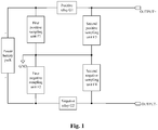
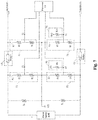
- Fig. 1 is a schematic diagram showing a structure of a battery detection circuit according to an embodiment of the present disclosure.
- the battery detection circuit may include a positive relay G1, a negative relay G2, a first positive sampling unit F1, a first negative sampling unit F2, a second positive sampling unit F3, a second negative sampling unit F4, and a reference voltage terminal GND
- the positive relay may be connected to a positive electrode of a power battery pack to be detected; the negative relay may be connected to a negative electrode of the power battery pack to be detected; and each of the first positive sampling unit, the first negative sampling unit, the second positive sampling unit, and the second negative sampling unit may be connected to the reference voltage terminal.
- the first positive sampling unit may be configured to acquire a first positive sampled signal of the battery pack at a first terminal of the positive relay; the first negative sampling unit may be configured to acquire a first negative sampled signal of the battery pack at a first terminal of the negative relay; the second positive sampling unit may be configured to acquire a second positive sampled signal of the battery pack at a second terminal of the positive relay; the second negative sampling unit may be configured to acquire a second negative sampled signal of the battery pack at a second terminal of the negative relay.
- the sampling units and the battery pack to be detected may be connected to the same reference voltage terminal.
- the isolation unit needs to be additionally provided for the sampling unit when the sampling unit and the battery pack are connected to different reference voltage terminals, the structure of the circuit according to the embodiment can be simplified, and meanwhile, the new interference signal introduced by additionally providing the isolation unit can be avoided and thus the accuracy of the sampled signals can be improved.
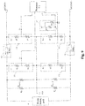
- Fig. 2 is a schematic diagram showing the structure of the battery detection circuit according to another embodiment of the present disclosure. As shown in Fig. 2, Fig. 2 differs from Fig. 1 in that, in some embodiments, the battery detection circuit may further include a first positive sampling point S1, a first negative sampling point S2, a second positive sampling point S3, a second negative sampling point S4, a first voltage pull-up unit F5, and a second voltage pull-up unit F6.
- the embodiments of the present disclosure are not limited to the description in the above embodiment and the specific units shown in Fig. 2 .
- the battery detection circuit may include only a portion of the units therein. That is, the battery detection circuit in the embodiments of the present disclosure may include a more flexible unit configuration, which will be described below in connection with specific embodiments.
- the battery detection circuit may further include the first positive sampling point, the first negative sampling point, the second positive sampling point, and the second negative sampling point.
- the first positive sampling unit may be further configured to provide the first positive sampled signal to the first positive sampling point; the first negative sampling unit may be further configured to provide the first negative sampled signal to the first negative sampling point; the second positive sampling unit may be further configured to provide the second positive sampled signal to the second positive sampling point; and the second negative sampling unit may be further configured to provide the second negative sampled signal to the second negative sampling point.
- a terminal of the first positive sampling unit F1 may be connected to the first terminal of the positive relay G1 and the positive electrode of the battery pack to be detected; and the other terminal of the first positive sampling unit F1 may be connected to the first positive sampling point S1 and the reference voltage terminal GND
- a terminal of the first negative sampling unit F2 may be connected to the first terminal of the negative relay G2 and the negative electrode of the battery pack to be detected; and the other terminal of the first negative sampling unit F2 may be connected to the first negative sampling point S2 and the reference voltage terminal GND
- a terminal of the second positive sampling unit F3 may be connected to the second terminal of the positive relay G1; and the other terminal of the second positive sampling unit F3 may be connected to the second positive sampling point S3 and the reference voltage terminal GND
- a terminal of the second negative sampling unit F4 may be connected to the second terminal of the negative relay G2; and the other terminal of the second negative sampling unit F4 may be connected to the second negative sampling point S4 and the reference voltage terminal GND
- an actual voltage at the reference voltage terminal GND may be set in accordance with working scene and demand of a high voltage sampling circuit.
- the voltage at the reference voltage terminal GND can be regarded as the reference voltage of the battery detection circuit in the embodiment.
- the reference voltage at the reference voltage terminal GND can be regarded as relative 0V.
- the reference voltage 6V can be recorded as 0V
- the voltage of the sampled signal acquired at the first positive sampling point S1 can be recorded as 16V
- all of a sampled voltage U SP1 of the first positive sampled signal at the first positive sampling point S1, a sampled voltage U SP2 of the first negative sampled signal at the first negative sampling point S2, a sampled voltage U SP3 of the second positive sampled signal at the second positive sampling point S3 and a sampled voltage U SP4 of the second negative sampled signal at the second negative sampling point S4 may share a same reference voltage.
- the reference voltage terminal may be a low voltage ground.
- all of the first positive sampling unit F1, the first negative sampling unit F2, the second positive sampling unit F3, the second negative sampling unit F4 and the power battery pack to be detected may be connected to the common low voltage ground.
- the voltages may be detected by the first positive sampling unit F1, the first negative sampling unit F2, the second positive sampling unit F3 and the second negative sampling unit F4.
- these sampling units employ the same reference voltage (e.g. they are connected to the common low voltage ground)
- both the sampled voltage U SP2 of the first negative sampled signal at the first negative sampling point S2 and the sampled voltage U SP4 of the second negative sampled signal at the second negative sampling point S4 may be lower than the voltage (i.e. relative 0V) at the reference voltage terminal GND because of the voltage drop of the current.
- both the sampled voltage U SP2 and the sampled voltage U SP4 may be recorded as a negative voltage.
- the battery detection circuit may further include the first voltage pull-up unit F5 and the second voltage pull-up unit F6.
- the first voltage pull-up unit F5 may be connected to the first negative sampling point S2, and the first voltage pull-up unit F5 may be configured to pull up the first negative sampled signal to be a positive voltage signal.
- the second voltage pull-up unit F6 may be connected to the second negative sampling point S4, and the second voltage pull-up unit F6 may be configured to pull up the second negative sampled signal to be a positive voltage signal.
- the voltage of the first negative sampled signal at the first negative sampling point S2 and the voltage of the second negative sampled signal at the second negative sampling point S4 are pulled up by a preset pull-up voltage value, so that both the output voltage U SP2 of the first negative sampled signal at the first negative sampling point S2 and the output voltage U SP4 of the second negative sampled signal at the second negative sampling point S4 may be higher than the voltage at the reference voltage terminal. That is, after the voltage pull-up process, both the voltage U SP2 of the first negative sampled signal at the first negative sampling point S2 and the voltage U SP4 of the second negative sampled signal at the second negative sampling point S4 may be recorded as a positive voltage.
- the battery detection circuit may implement voltage sampling for a high voltage circuit, insulation detection for the power battery pack to be detected and relay diagnosis for the battery detection circuit, based on the first positive sampled signal acquired from the first positive sampling point S1, the first negative sampled signal acquired from the first negative sampling point S2, the second positive sampled signal acquired from the second positive sampling point S3 and the second negative sampled signal acquired from the second negative sampling point S4.
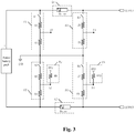
- Fig. 3 is a schematic diagram showing a structure of a battery detection circuit according to an exemplary embodiment of the present disclosure.
- Fig. 3 schematically shows specific structures of the first positive sampling unit F1, the first negative sampling unit F2, the second positive sampling unit F3, the second negative sampling unit F4, the first voltage pull-up unit F5, and the second voltage pull-up unit F6.
- the first positive sampling unit F1 may include a first resistor network R1 and a second resistor network R2 in series.
- a terminal of the first resistor network R1 may be connected to the first terminal of the positive relay G1 and the positive electrode of the battery pack to be detected, and the other terminal of the first resistor network R1 may be connected to the first positive sampling point S1 and a terminal of the second resistor network R2.
- the other terminal of the second resistor network R2 may be connected to the reference voltage terminal GND
- the resistor network form and the resistance value of the first resistor network R1 may be the same as the resistor network form and the resistance value of the second resistor network R2.
- the first resistor network R1 and the second resistor network R2 may function as a divider.
- the range of the first positive sampled signal at the first positive sampling point S1 can be adjusted by adjusting the resistance value of the first resistor network R1 and the resistance value of the second resistor network R2.
- the first negative sampling unit F2 may include a third resistor network R3 and a fourth resistor network R4 in series.
- a terminal of the third resistor network R3 may be connected to the reference voltage terminal GND, and the other terminal of the third resistor network R3 may be connected to the first negative sampling point S2 and a terminal of the fourth resistor network R4.
- the other terminal of the fourth resistor network R4 may be connected to the first terminal of the negative relay G2 and the negative electrode of the battery pack to be detected.
- the resistor network form and the resistance value of the third resistor network R3 may be the same as the resistor network form and the resistance value of the fourth resistor network R4.
- the third resistor network R3 and the fourth resistor network R4 may function as a divider.
- the range of the first negative sampled signal at the first negative sampling point S2 can be adjusted by adjusting the resistance value of the third resistor network R3 and the resistance value of the fourth resistor network R4.
- the second positive sampling unit F3 may include a fifth resistor network R5 and a sixth resistor network R6 in series.
- a terminal of the fifth resistor network R5 may be connected to the second terminal of the positive relay G1, and the other terminal of the fifth resistor network R5 may be connected to the second positive sampling point S3 and a terminal of the sixth resistor network R6.
- the other terminal of the sixth resistor network R6 may be connected to the reference voltage terminal GND
- the resistor network form and the resistance value of the fifth resistor network R5 may be the same as the resistor network form and the resistance value of the sixth resistor network R6.
- the fifth resistor network R5 and the sixth resistor network R6 may function as a divider.
- the range of the second positive sampled signal at the second positive sampling point S3 can be adjusted by adjusting the resistance value of the fifth resistor network R5 and the resistance value of the sixth resistor network R6.
- the second negative sampling unit F4 may include a seventh resistor network R7 and an eighth resistor network R8 in series.
- a terminal of the seventh resistor network R7 may be connected to the reference voltage terminal GND, and the other terminal of the seventh resistor network R7 may be connected to the second negative sampling point S4 and a terminal of the eighth resistor network R8.
- the other terminal of the eighth resistor network R8 may be connected to the second terminal of the negative relay G2.
- the resistor network form and the resistance value of the seventh resistor network R7 may be the same as the resistor network form and the resistance value of the eighth resistor network R8.
- the seventh resistor network R7 and the eighth resistor network R8 may function as a divider.
- the range of the second negative sampled signal at the second negative sampling point S4 can be adjusted by adjusting the resistance value of the seventh resistor network R7 and the resistance value of the eighth resistor network R8.
- the first voltage pull-up unit F5 may further include a first DC (Direct Current) voltage source DV1 and a ninth resistor network R9.
- a terminal of the ninth resistor network R9 may be connected to the first negative sampling point S2, and the other terminal of the ninth resistor network R9 may be connected to the first DC voltage source DV1.
- the first DC voltage source DV1 may generate a pull-up voltage U1.
- U1 may be a preset value and U1 may be greater than the voltage at the reference voltage terminal GND
- the second voltage pull-up unit F6 may further include a second DC voltage source DV2 and a tenth resistor network R10.
- a terminal of the tenth resistor network R10 may be connected to the second negative sampling point S4, and the other terminal of the tenth resistor network R10 may be connected to the second DC voltage source DV2.
- the second DC voltage source DV2 may generate a pull-up voltage U2.
- U2 may be a preset value and U2 may be greater than the voltage at the reference voltage terminal GND
- the pull-up voltage U1 and the pull-up voltage U2 can be set to have a same pull-up voltage value.
- each of the first resistor network R1 to the tenth resistor network R10 may include a single resistor. In some other embodiments, each of the first resistor network R1 to the tenth resistor network R10 may include two or more resistors in series and/or in parallel.
- resistor network form and the resistance value of each of the first resistor network R1 to the tenth resistor network RIO may be set in the actual application scenario of the battery detection according to the actual situation.
- the resistor network form and the resistance value of each of the first resistor network R1 to the tenth resistor network RIO may be determined based on the demanded sampling accuracy and sampling range for the high voltage sampling process conducted by the battery detection circuit, the sampling range limit and the achievable sampling accuracy of the sampling units in the above described embodiments of the battery detection circuit, the tolerance range of operating voltage of components in the battery detection circuit, and the like.
- the first positive sampling unit F1 may further include a first switch K1.
- a terminal of the first resistor network R1 may be connected, via the first switch K1, to the positive electrode of the power battery pack to be detected.
- the first positive sampling point S1 provides the first positive sampled signal or not, by turning on or turning off the first switch K1.
- the first positive sampling point S1 may provide the first positive sampled signal.
- the first switch K1 is turned off, the first positive sampling point S1 may stop providing the first positive sampled signal.
- the first negative sampling unit F2 may further include a second switch K2.
- a terminal of the third resistor network R3 may be connected to the reference voltage terminal GND via the second switch K2.
- the first negative sampling point S2 provides the first negative sampled signal or not, by turning on or turning off the second switch K2.
- the first negative sampling point S2 may provide the first negative sampled signal.
- the second switch K2 is turned off, the first negative sampling point S2 may stop providing the first negative sampled signal.
- the second positive sampling unit F3 may further include a third switch K3.
- a terminal of the fifth resistor network R5 may be connected to the second terminal of the positive relay G1 via the third switch K3.
- the second positive sampling point S3 provides the second positive sampled signal or not, by turning on or turning off the third switch K3.
- the third switch K3 When the third switch K3 is turned on, the second positive sampling point S3 may provide the second positive sampled signal.
- the third switch K3 When the third switch K3 is turned off, the second positive sampling point S3 may stop providing the second positive sampled signal.
- the second negative sampling unit F4 may further include a fourth switch K4.
- a terminal of the seventh resistor network R7 may be connected to the reference voltage terminal GND via the fourth switch K4.
- the second negative sampling point S4 provides the second negative sampled signal or not, by turning on or turning off the fourth switch K4.
- the fourth switch K4 When the fourth switch K4 is turned on, the second negative sampling point S4 may provide the second negative sampled signal.
- the fourth switch K4 When the fourth switch K4 is turned off, the second negative sampling point S4 may stop providing the second negative sampled signal.
- each of the first positive sampling point S1, the first negative sampling point S2, the second positive sampling point S3 and the second negative sampling point S4 may be connected to a sampling unit for implementing the sampling process.
- the sampling unit may be an Analog to Digital Converter (ADC).
- the ADC 1 may be connected to the first positive sampling point S1 via a sampling line SP1 to acquire the voltage on the second resistor network through the first positive sampled signal supplied from the first positive sampling point S1.
- the ADC 2 may be connected to the first negative sampling point S2 via a sampling line SP2 to acquire the voltage on the third resistor network through the first negative sampled signal supplied from the first negative sampling point S2.
- the ADC 3 may be connected to the second positive sampling point S3 via a sampling line SP3 to acquire the voltage on the sixth resistor network through the second positive sampled signal supplied from the second positive sampling point S3.
- the ADC 4 may be connected to the second negative sampling point S4 via a sampling line SP4 to acquire the voltage on the seventh resistor network through the second negative sampled signal supplied from the second negative sampling point S4.
- the battery detection circuit according to the embodiment of the present disclosure may provide an integral circuitry to implement the high voltage sampling, the insulation detection and the relay diagnosis. With such a battery detection circuit, it is possible to acquire the voltage of the battery pack, detect an insulation resistance value of the battery pack and diagnose whether the relay has failed.
- the structure of the circuit may be simplified and the cost of the circuit may be reduced.
- the battery to be detected and each of the first positive sampling unit F1, the first negative sampling unit F2, the second positive sampling unit F3 and the second negative sampling unit F4 may be connected to a common ground.
- the isolation unit for isolating the sampled signal thereby simplifying the circuit structure, reducing the error caused by isolating the sampled signal, and thus improving the accuracy of the voltage of the sampled signal.
- Fig. 4 is a schematic diagram showing a structure of the battery detection circuit according to the further embodiment of the present disclosure.
- a same reference number may indicate a same element.
- the battery detection circuit shown in Fig. 4 is almost the same as the battery detection circuit shown in Fig. 2 and only has the following differences.
- the first negative sampling unit F2 and the second negative sampling unit F4 may be connected to the voltage pull-up unit F7.
- the voltage pull-up unit F7 may pull up the sampled voltage of the first negative sampled signal and the sample voltage of the second negative sampled signal to be a positive voltage signal.
- the battery detection circuit may further include a first fixed resistor network R net1 .
- a first terminal of the first fixed resistor network R net1 may be connected to the positive electrode of the power battery pack to be detected.
- a second terminal of the first fixed resistor network R net1 may be connected to the reference voltage terminal GND
- the battery management system may further include a second fixed resistor network R net2 .
- a first terminal of the second fixed resistor network R net2 may be connected to the negative electrode of the power battery pack to be detected.
- a second terminal of the second fixed resistor network R net2 may be connected to the reference voltage terminal GND
- the battery management system may include both the first fixed resistor network R net1 and the second fixed resistor network R net2 .
- Fig. 4 also schematically shows positions of a positive insulation resistance and a negative insulation resistance of the power battery pack to be detected in the circuit diagram of the battery detection circuit.
- R p indicates the positive insulation resistance of the power battery pack
- R n indicates the negative insulation resistance of the power battery pack.
- a terminal of R p may be connected to the positive electrode of the power battery pack to be detected, and the other terminal of R p may be connected to the reference voltage terminal GND; a terminal of R n may be connected to the reference voltage terminal GND, and the other terminal of R n may be connected to the negative electrode of the power battery pack to be detected.
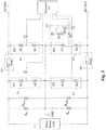
- Fig. 5 is a circuit diagram of the battery detection circuit according to the further exemplary embodiment of the present disclosure.
- Fig. 5 schematically shows specific structures of the first positive sampling unit F1, the first negative sampling unit F2, the second positive sampling unit F3, the second negative sampling unit F4, the voltage pull-up unit F7, the first fixed resistor network R net1 and the second fixed resistor network R net2 .
- the voltage pull-up unit may include a DC voltage source DV, the ninth resistor network R9 and the tenth resistor network R10.
- a terminal of the ninth resistor network R9 may be connected to the first negative sampling point S2, and the other terminal of the ninth resistor network R9 may be connected to the DC voltage source DV.
- the DC voltage source DV and the ninth resistor network R9 may generate the pull-up voltage U1.
- U1 may be a preset value and U1 may be greater than the voltage at the reference voltage terminal GND
- a terminal of the tenth resistor network R10 may be connected to the second negative sampling point S4, and the other terminal of the tenth resistor network RIO may be connected to the DC voltage source DV.
- the DC voltage source DV and the tenth resistor network RIO may generate the pull-up voltage U2.
- U2 may be a preset value and U2 may be greater than the voltage at the reference voltage terminal GND
- the pull-up voltage U1 and the pull-up voltage U2 can be set to have a same pull-up voltage value.
- each of the sampled voltage of the first negative sampled signal and the sampled voltage of the second negative sampled signal may be pulled up to be a positive voltage signal via the voltage pull-up unit F7 according to the embodiments of the present disclosure.
- each of the first fixed resistor network R net1 and the second fixed resistor network R net2 may include a single resistor. In some other embodiments, each of the first fixed resistor network R net1 and the second fixed resistor network R net2 may include two or more resistors in series and/or in parallel.
- the resistor network form and the resistance value of the first fixed resistor network R net1 may be the same as the resistor network form and the resistance value of the second fixed resistor network R net2 .
- Fig. 5 also schematically shows positions of the positive insulation resistance and the negative insulation resistance of the power battery pack to be detected in the circuit diagram of the battery detection circuit.
- R p indicates the positive insulation resistance of the power battery pack
- R n indicates the negative insulation resistance of the power battery pack.
- a terminal of the positive insulation resistance R p may be connected to the positive electrode of the power battery pack to be detected, and the other terminal of R p may be connected to the reference voltage terminal GND; a terminal of the negative insulation resistance R n may be connected to the reference voltage terminal GND, and the other terminal of R n may be connected to the negative electrode of the power battery pack to be detected.
- a battery management system according to an embodiment of the present disclosure will be described in detail below.
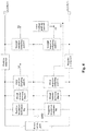
- Fig. 6 is a schematic diagram showing a structure of the battery management system in an embodiment.
- the battery management system may include the battery detection circuit in the above embodiments and a processor C1 that is connected to the battery detection circuit.
- Fig. 6 also schematically shows positions of the positive insulation resistance and the negative insulation resistance of the power battery pack to be detected in the circuit diagram of the battery detection circuit.
- a terminal of R p may be connected to the positive electrode of the power battery pack to be detected, and the other terminal of R p may be connected to the reference voltage terminal GND; a terminal of R n may be connected to the reference voltage terminal GND, and the other terminal of R n may be connected to the negative electrode of the power battery pack to be detected.
- the processor C1 in the battery management system may be directly connected to the first positive sampling point S1, the first negative sampling point S2, the second positive sampling point S3, and the second negative sampling point S4.
- the processor C1 may have the function of converting each of the first positive sampled signal, the first negative sampled signal, the second positive sampled signal, and the second negative sampled signal to a digital signal.
- the battery management system may further include an ADC1.
- a terminal of the ADC1 may be connected to the first positive sampling point S1, and the other terminal of the ADC1 may be connected to the processor C1.
- the ADC1 may be configured to convert the first positive sampled signal into a digital signal.
- the battery management system may further include an ADC2.
- a terminal of the ADC2 may be connected to the first negative sampling point S2, and the other terminal of the ADC2 may be connected to the processor C1.
- the ADC2 may be configured to convert the first negative sampled signal into a digital signal.
- the battery management system may further include an ADC3.
- a terminal of the ADC3 may be connected to the second positive sampling point S3, and the other terminal of the ADC3 may be connected to the processor C1.
- the ADC3 may be configured to convert the second positive sampled signal into a digital signal.
- the battery management system may further include an ADC4.
- a terminal of the ADC4 may be connected to the second negative sampling point S4, and the other terminal of the ADC4 may be connected to the processor C1.
- the ADC4 may be configured to convert the second negative sampled signal into a digital signal.
- the ADC1, the ADC2, the ADC3 and the ADC4 may be connected to the processor C1, so that the processor C1 may operate according to each of the digital signal of the positive sampled signal, the digital signal of the first negative sampled signal, the digital signal of the second positive sampled signal, and the digital signal of the second negative sampled signal.
- the battery management system may implement the high voltage sampling process for the power battery pack, detect the insulation resistance value of the power battery pack and diagnose whether the relay has failed.
- the voltage between the first terminal of the positive relay G1 and the first terminal of the negative relay G2 may be referred to as a relay-input voltage of the power battery pack to be detected, and the voltage between the second terminal of the positive relay G1 and the second terminal of the negative relay G2 may be referred to as a relay-output voltage of the power battery pack to be detected.
- the processor C1 may calculate the relay-input voltage and the relay-output voltage of the power battery pack to be detected, based on the first positive sampled signal, the first negative sampled signal, the second positive sampled signal, and the second negative sampled signal.
- the high voltage sampling may be implemented as follows.
- the first positive sampling point S1 may provide the first positive sampled signal; the first negative sampling point S2 may provide the first negative sampled signal; the second positive sampling point S3 may stop providing the second positive sampled signal; and the second negative sampling point S4 may stop providing the second negative sampled signal.
- the processor C1 may calculate the voltage at the first terminal of the positive relay G1 based on the first positive sampled signal, which is the voltage of the power battery pack at the first terminal of the positive relay G1.
- the voltage may also be referred to as a positive-terminal-relay-input voltage of the power battery pack.
- the processor C1 may calculate the voltage at the first terminal of the negative relay G2 based on the first negative sampled signal, which is the voltage of the power battery pack at the first terminal of the negative relay G2.
- the voltage may also be referred to as a negative-terminal-relay-input voltage of the power battery pack.
- the processor C1 may calculate the relay-input voltage of the power battery pack, based on the voltage at the first terminal of the positive relay G1 and the voltage at the first terminal of the negative relay G2.
- the processor C1 may calculate the relay-input voltage of the power battery pack, based on the positive-terminal-relay-input voltage and the negative-terminal-relay-input voltage of the power battery pack.
- the sampled voltage U sp1 of the first positive sampled signal may be obtained from the first positive sampled signal supplied from the first positive sampling point S1. Based on the sampled voltage U sp1 of the first positive sampled signal, the first resistor network R1 and the second resistor network R2 in series, the voltage of the power battery pack at the first terminal of the positive relay G1 (i.e. the positive-terminal-relay-input voltage of the power battery pack) may be calculated according to the Ohm's Law.
- the sampled voltage U sp2 of the first negative sampled signal may be obtained from the first negative sampled signal supplied from the first negative sampling point S2.
- the third resistor network R3 and the fourth resistor network R4 in series the voltage of the power battery pack at the first terminal of the negative relay G2 (i.e. the negative-terminal-relay-input voltage of the power battery pack) may be calculated according to the Ohm's Law.
- the relay-input voltage of the power battery pack may be obtained by calculating a sum of the positive-terminal-relay-input voltage of the power battery pack and the negative-terminal-relay-input voltage of the power battery pack.
- the high voltage sampling may be implemented as follows.
- the first positive sampling point S1 may stop providing the first positive sampled signal; the first negative sampling point S2 may stop providing the first negative sampled signal; the second positive sampling point S3 may provide the second positive sampled signal; and the second negative sampling point S4 may provide the second negative sampled signal.
- the processor C1 may calculate the voltage at the second terminal of the positive relay G1 based on the second positive sampled signal, which is the voltage of the power battery pack at the second terminal of the positive relay G1.
- the voltage may also be referred to as a positive-terminal-relay-output voltage of the power battery pack.
- the processor C1 may calculate the voltage at the second terminal of the negative relay G2 based on the second negative sampled signal, which is the voltage of the power battery pack at the second terminal of the negative relay G2.
- the voltage may also be referred to as a negative-terminal-relay-output voltage of the power battery pack.
- the processor C1 may calculate the relay-output voltage of the power battery pack, based on the voltage at the second terminal of the positive relay G1 and the voltage at the second terminal of the negative relay G2.
- the processor C1 may calculate the relay-output voltage of the power battery pack, based on the positive-terminal-relay-output voltage and the negative-terminal-relay-output voltage of the power battery pack.
- the sampled voltage U sp3 of the second positive sampled signal may be obtained from the second positive sampled signal supplied from the second positive sampling point S3.
- the voltage of the power battery pack at the second terminal of the positive relay G1 i.e. the positive-terminal-relay-output voltage of the power battery pack
- the Ohm's Law the Ohm's Law
- the sampled voltage U sp4 of the second negative sampled signal may be obtained from the second negative sampled signal supplied from the second negative sampling point S4.
- the seventh resistor network R7 and the eighth resistor network R8 in series the voltage of the power battery pack at the second terminal of the negative relay G2 (i.e. the negative-terminal-relay-output voltage of the power battery pack) may be calculated according to the Ohm's Law.
- the relay-output voltage of the power battery pack may be obtained by calculating a sum of the positive-terminal-relay-output voltage of the power battery pack and the negative-terminal-relay-output voltage of the power battery pack.
- the battery detection circuit of the embodiment may be utilized to calculate the relay-input voltage and the relay-output voltage of the power battery pack based on the sampled voltage U sp1 , the sampled voltage U sp2 , the sampled voltage U sp3 , and the sampled voltage U sp4 , so as to implement the high voltage sampling.
- an absolute value of a difference between the voltage at the first terminal of the positive relay G1 and the voltage of the second terminal of the positive relay G1 may be compared with a voltage threshold of the positive relay G1, to obtain a comparison result for determining an operating state of the positive relay G1.
- the voltage at the first terminal of the positive relay G1 i.e. the positive-terminal-relay-input voltage U B+ (input) of the power battery pack
- the voltage at the second terminal of the positive relay G1 i.e. the positive-terminal-relay-output voltage U B+ (output) of the power battery pack
- U relay+ is a preset voltage drop of the relay coil at a positive terminal of the power battery pack to be detected.
- the positive relay G1 when the positive relay G1 is controlled to be turned on, if the absolute value of the difference between the voltage at the first terminal of the positive relay G1 and the voltage of the second terminal of the positive relay G1 is smaller than or equals to the preset voltage drop of the relay coil at the positive terminal of the power battery pack, it may be determined that the positive relay G1 is in the normal operating state.
- an absolute value of a difference between the voltage at the first terminal of the negative relay G2 and the voltage of the second terminal of the negative relay G2 may be compared with a voltage threshold of the negative relay G2, to obtain a comparison result for determining an operating state of the negative relay G2.
- the voltage at the first terminal of the negative relay G2 i.e. the negative-terminal-relay-input voltage U B- (input) of the power battery pack
- the voltage at the second terminal of the negative relay G2 i.e. the negative-terminal-relay-output voltage U B- (output) of the power battery pack
- U relay- is a preset voltage drop of the relay coil at a negative terminal of the power battery pack to be detected.
- the operating state of the relay coil at the positive terminal of the power battery pack can be diagnosed according to the positive-terminal-relay-input voltage and the positive-terminal-relay-output voltage of the power battery pack obtained in the high voltage sampling process and the preset voltage drop of the relay coil at the positive terminal of the power battery pack; and the operating state of the relay coil at the negative terminal of the power battery pack can be diagnosed according to the negative-terminal-relay-input voltage and the negative-terminal-relay-output voltage of the power battery pack obtained in the high voltage sampling process and the preset voltage drop of the relay coil at the negative terminal of the power battery pack.
- the battery management system may include the battery detection circuit in the above embodiments and the processor C1 that is connected to the battery detection circuit.
- Fig. 7 also schematically shows the positions of the positive insulation resistance and the negative insulation resistance of the power battery pack to be detected in the circuit diagram of the battery detection circuit.
- R p indicates the positive insulation resistance of the power battery pack
- R n indicates the negative insulation resistance of the power battery pack.
- a terminal of R p may be connected to the positive electrode of the power battery pack to be detected, and the other terminal of R p may be connected to the reference voltage terminal GND; a terminal of R n may be connected to the reference voltage terminal GND, and the other terminal of R n may be connected to the negative electrode of the power battery pack to be detected.
- the processor C1 may simultaneously turn on the first switch K1 and the second switch K2.
- the state of the switches may be referred to as a first switch state.
- a positive terminal voltage U p0 and a negative terminal voltage U n0 of the power battery pack under the first switch state may be calculated based on the first positive sampled signal acquired from the first positive sampling point S1 and the first negative sampled signal acquired from the first negative sampling point S2 under the first switch state.
- the processor C1 may turn on the first switch K1 and turn off the second switch K2.
- the state of the switches may be referred to as a second switch state.
- a positive terminal voltage U p1 of the power battery pack under the second switch state may be calculated based on the first positive sampled signal acquired under the second switch state.
- the processor C1 may turn off the first switch K1 and turn on the second switch K2.
- the state of the switches may be referred to as a third switch state.
- a negative terminal voltage U n2 of the power battery pack under the third switch state may be calculated based on the first negative sampled signal acquired under the third switch state.
- the processor C1 may calculate the positive insulation resistance value and the negative insulation resistance value of the power battery pack, based on the positive terminal voltage U p0 of the power battery pack under the first switch state, the negative terminal voltage U n0 of the power battery pack under the first switch state, the positive terminal voltage U p1 of the power battery pack under the second switch state, and the negative terminal voltage U n2 of the power battery pack under the third switch state.
- the processor C1 may obtain the following Formula (5) based on the sampled voltage U mp0 of the first positive sampled signal and the sampled voltage U mn0 of the first negative sampled signal acquired under the first switch state.
- U p 0 U mp 0
- R 1 + R 2 R 2 U n 0 U mn 0
- U p0 indicates the positive terminal voltage of the power battery pack under the first switch state
- U n0 indicates the negative terminal voltage of the power battery pack under the first switch state
- R 1 indicates the resistance value of the first resistor network
- R 2 indicates the resistance value of the second resistor network
- R 3 indicates the resistance value of the third resistor network
- R 4 indicates the resistance value of the fourth resistor network
- R p indicates the positive insulation resistance value of the power battery pack
- R n indicates the negative insulation resistance value of the power battery pack.
- the processor C1 may obtain the following Formula (6) based on the sampled voltage U mp1 of the first positive sampled signal acquired under the second switch state.
- U p 1 U mp 1 R 1 + R 2 R 2
- U n 1 U B
- U p 1 + R 2 R 1 + R 2 + R p R n U B U n 1 + U p 1
- U p1 indicates the positive terminal voltage of the power battery pack under the second switch state
- U n1 indicates the negative terminal voltage of the power battery pack under the second switch state
- R 1 indicates the resistance value of the first resistor network
- R 2 indicates the resistance value of the second resistor network
- R p indicates the positive insulation resistance value of the power battery pack
- R n indicates the negative insulation resistance value of the power battery pack.
- the processor C1 may obtain the following Formula (7) based on the sampled voltage U mn2 of the first negative sampled signal acquired under the third switch state.
- U n 2 U mn 2 R 3 + R 4 R 3
- U p2 indicates the positive terminal voltage of the power battery pack under the third switch state
- U n2 indicates the negative terminal voltage of the power battery pack under the third switch state
- R 3 indicates the resistance value of the third resistor network
- R 4 indicates the resistance value of the fourth resistor network
- R p indicates the positive insulation resistance value of the power battery pack
- R n indicates the negative insulation resistance value of the power battery pack.
- the positive insulation resistance R p and the negative insulation resistance R n of the power battery pack may be obtained by combining the Formulas (5), (6), and (7).
- R p ⁇ R a ⁇ R b ⁇ R a U mp 1 + R b U mp 1 ⁇ R b U B U mn 2
- R n ⁇ R a ⁇ R b ⁇ R a U mn 2 + R b U mn 2 ⁇ R b U B U mp 1
- Fig. 8 is a schematic diagram showing a structure of a battery management system according to another embodiment of the present disclosure
- Fig. 9 is a circuit diagram of the battery management system according to another embodiment of the present disclosure.
- the battery management system may include the battery detection circuit and the processor C1 that is connected to the battery detection circuit.
- experimental results show that when the difference between the positive insulation resistance R p and the negative insulation resistance R n is large, the sampling accuracy of the battery detection circuit is low; when the difference between the positive insulation resistance R p and the negative insulation resistance R n is small, the sampling accuracy of the battery detection circuit is high.
- the battery detection circuit may include at least one of the first fixed resistor network R net1 and the second fixed resistor network R net2 .
- the processor C1 may obtain the following Formula (9) based on the sampled voltage U mp0 of the first positive sampled signal and the sampled voltage U mn0 of the first negative sampled signal acquired under the first switch state.
- U p0 indicates the positive terminal voltage of the power battery pack under the first switch state
- U n0 indicates the negative terminal voltage of the power battery pack under the first switch state
- R 1 indicates the resistance value of the first resistor network
- R 2 indicates the resistance value of the second resistor network
- R 3 indicates the resistance value of the third resistor network
- R 4 indicates the resistance value of the fourth resistor network
- R p indicates the positive insulation resistance value of the power battery pack
- R n indicates the negative insulation resistance value of the power battery pack
- R net1 indicates the resistance value of the first fixed resistor network
- R net2 indicates the resistance value of the second fixed resistor network
- R p // R net 1 indicates the parallel resistance value of the positive insulation resistance and the first fixed resistor network
- R n // R net 2 indicates the parallel resistance value of the negative insulation resistance and the second fixed resistor network.
- the processor C1 may obtain the following Formula (10) based on the sampled voltage U mp1 of the first positive sampled signal acquired under the second switch state.
- U B U n 1 + U p 1
- U p1 indicates the positive terminal voltage of the power battery pack under the second switch state
- U n1 indicates the negative terminal voltage of the power battery pack under the second switch state
- R 1 indicates the resistance value of the first resistor network
- R 2 indicates the resistance value of the second resistor network
- R p indicates the positive insulation resistance value of the power battery pack
- R n indicates the negative insulation resistance value of the power battery pack
- R p // R net 1 indicates the parallel resistance value of the positive insulation resistance and the first fixed resistor network
- R n // R net 2 indicates the parallel resistance value of the negative insulation resistance and the second fixed resistor network.
- the processor C1 may obtain the following Formula (11) based on the sampled voltage U mn2 of the first negative sampled signal acquired under the third switch state.
- U n 2 U mn 2 R 3 + R 4 R 3
- U p 2 U B + U n 2
- U n 2 R n / / R net 2 R 3 + R 4 R 3 + R 4 + R n / / R net 2 R p / / R net 1
- U B U n 2 + U p 2
- U p2 indicates the positive terminal voltage of the power battery pack under the third switch state
- U n2 indicates the negative terminal voltage of the power battery pack under the third switch state
- R 3 indicates the resistance value of the third resistor network
- R 4 indicates the resistance value of the fourth resistor network
- R p indicates the positive insulation resistance value of the power battery pack
- R n indicates the negative insulation resistance value of the power battery pack
- R p // R net 1 indicates the parallel resistance value of the positive insulation resistance and the first fixed resistor network
- R n // R net 2 indicates the parallel resistance value of the negative insulation resistance and the second fixed resistor network.
- the positive insulation resistance R p and the negative insulation resistance R n of the power battery pack may be obtained by combining the Formulas (9), (10), and (11).
- the sampling accuracy of the battery detection circuit may be improved by adding the fixed resistor network R net1 and the fixed resistor network R net2 as described above. Also, due to the low price of resistors, the cost-performance ratio of the battery detection circuit can be improved by reducing the cost.
- an integral design for implementing the high voltage sampling, the insulation detection, and the relay diagnosis for the power battery pack to be detected may be conceived.
- the issues such as complex structure, high cost and low accuracy caused by separately implementing the high voltage sampling, the insulation detection and the relay diagnosis can be solved.
- the circuit structure can be simplified, the circuit cost can be reduced and the accurate sampling and detection results can be obtained.
Landscapes
- Physics & Mathematics (AREA)
- General Physics & Mathematics (AREA)
- Secondary Cells (AREA)
Claims (14)
- Batterieerfassungsschaltung, gekennzeichnet dadurch, dass sie ein positives Relais (G1), ein negatives Relais (G2), eine erste positive Abtasteinheit (F1), eine erste negative Abtasteinheit (F2), eine zweite positive Abtasteinheit (F3), eine zweite negative Abtasteinheit (F4) und einen Referenzspannungsanschluss (GND), wobei:ein erster Anschluss des positiven Relais (G1) mit einer positiven Elektrode eines zu erfassenden Leistungsbatteriepacks verbunden ist, ein erster Anschluss des negativen Relais (G2) mit einer negativen Elektrode des zu erfassenden Leistungsbatteriepacks verbunden ist, und jede von der ersten positiven Abtasteinheit (F1), der ersten negativen Abtasteinheit (F2), der zweiten positiven Abtasteinheit (F3) und der zweiten negativen Abtasteinheit (F4) mit dem Referenzspannungsanschluss (GND) verbunden ist;die erste positive Abtasteinheit (F1) einen ersten Schalter (K1) umfasst und so konfiguriert ist, dass sie ein erstes positives Abtastsignal des zu erfassenden Leistungsbatteriepacks am ersten Anschluss des positiven Relais (G1) beim eingeschalteten ersten Schalter (K1) erfasst;die erste negative Abtasteinheit (F2) einen zweiten Schalter (K2) umfasst und so konfiguriert ist, dass sie ein erstes negatives Abtastsignal des zu erfassenden Leistungsbatteriepacks am ersten Anschluss des negativen Relais (G2) beim eingeschalteten zweiten Schalter (K2) erfasst; dadurch gekennzeichnet, dassdie zweite positive Abtasteinheit (F3) einen dritten Schalter (K3) umfasst und so konfiguriert ist, dass sie ein zweites positives Abtastsignal des zu erfassenden Leistungsbatteriepacks an einem zweiten Anschluss des positiven Relais (G1) beim eingeschalteten dritten Schalter (K3) erfasst;die zweite negative Abtasteinheit (F4) einen vierten Schalter (K4) umfasst und so konfiguriert ist, dass sie ein zweites negatives Abtastsignal des zu erfassenden Leistungsbatteriepacks an einem zweiten Anschluss des negativen Relais (G2) beim eingeschalteten vierten Schalter (K4) erfasst;der Referenzspannungsanschluss eine Niederspannungsmasse ist;die Batterieerfassungsschaltung ferner mindestens eines von einem ersten Festwiderstandsnetzwerk (Rnet1) und einem zweiten Festwiderstandsnetzwerk (Rnet2) umfasst, wobei:ein erster Anschluss des ersten Festwiderstandsnetzwerks (Rnet1) mit der positiven Elektrode des zu erfassenden Leistungsbatteriepacks verbunden ist;ein zweiter Anschluss des ersten Festwiderstandsnetzwerks (Rnet1) mit dem Referenzspannungsanschluss (GND) verbunden ist;ein erster Anschluss des zweiten Festwiderstandsnetzwerks (Rnet2) mit der negativen Elektrode des zu erfassenden Leistungsbatteriepacks verbunden ist; undein zweiter Anschluss des zweiten Festwiderstandsnetzwerks (Rnet2) mit dem Referenzspannungsanschluss (GND) verbunden ist.
- Batterieerfassungsschaltung nach Anspruch 1, ferner umfassend einen ersten positiven Abtastpunkt (S1), einen ersten negativen Abtastpunkt (S2), einen zweiten positiven Abtastpunkt (S3) und einen zweiten negativen Abtastpunkt (S4), wobei:die erste positive Abtasteinheit (F1) ferner so konfiguriert ist, dass sie das erste positive Abtastsignal an den ersten positiven Abtastpunkt (S1) liefert;die erste negative Abtasteinheit (F2) ferner so konfiguriert ist, dass sie das erste negative Abtastsignal an den ersten negativen Abtastpunkt (S2) liefert;die zweite positive Abtasteinheit (F3) ferner so konfiguriert ist, dass sie das zweite positive Abtastsignal an den zweiten positiven Abtastpunkt (S3) liefert; unddie zweite negative Abtasteinheit (F4) ferner so konfiguriert ist, dass sie das zweite negative Abtastsignal an den zweiten negativen Abtastpunkt (S4) liefert.
- Batterieerfassungsschaltung nach Anspruch 2, wobei:ein Anschluss der ersten positiven Abtasteinheit (F1) mit dem ersten Anschluss des positiven Relais (G1) und der positiven Elektrode des zu erfassenden Leistungsbatteriepacks verbunden ist und der andere Anschluss der ersten positiven Abtasteinheit (F1) mit dem ersten positiven Abtastpunkt (S1) und dem Referenzspannungsanschluss (GND) verbunden ist;ein Anschluss der ersten negativen Abtasteinheit (F2) mit dem ersten Anschluss des negativen Relais (G2) und der negativen Elektrode des zu erfassenden Batteriepacks verbunden ist und der andere Anschluss der ersten negativen Abtasteinheit (F2) mit dem ersten negativen Abtastpunkt (S2) und dem Referenzspannungsanschluss (GND) verbunden ist;ein Anschluss der zweiten positiven Abtasteinheit (F3) mit dem zweiten Anschluss des positiven Relais (G1) verbunden ist und der andere Anschluss der zweiten positiven Abtasteinheit (F3) mit dem zweiten positiven Abtastpunkt (S3) und dem Referenzspannungsanschluss (GND) verbunden ist;ein Anschluss der zweiten negativen Abtasteinheit (F4) mit dem zweiten Anschluss des negativen Relais (G2) verbunden ist und der andere Anschluss der zweiten negativen Abtasteinheit (F4) mit dem zweiten negativen Abtastpunkt (S4) verbunden ist.
- Batterieerfassungsschaltung nach Anspruch 3, wobei:die erste positive Abtasteinheit (F1) ein erstes Widerstandsnetzwerk (R1) und ein zweites Widerstandsnetzwerk (R2) umfasst, die in Reihe geschaltet sind;ein Anschluss des ersten Widerstandsnetzwerks (R1) mit dem ersten Anschluss des positiven Relais (G1) und der positiven Elektrode des zu erfassenden Leistungsbatteriepacks verbunden ist, und der andere Anschluss des ersten Widerstandsnetzwerks (R1) mit dem ersten positiven Abtastpunkt (S1) und einem Anschluss des zweiten Widerstandsnetzwerks (R2) verbunden ist;der andere Anschluss des zweiten Widerstandsnetzwerks (R2) mit dem Referenzspannungsanschluss (GND) verbunden ist;die erste negative Abtasteinheit (F2) ein drittes Widerstandsnetzwerk (R3) und ein viertes Widerstandsnetzwerk (R4) umfasst, die in Reihe geschaltet sind;ein Anschluss des dritten Widerstandsnetzwerks (R3) mit dem Referenzspannungsanschluss (GND) verbunden ist, und der andere Anschluss des dritten Widerstandsnetzwerks (R3) mit dem ersten negativen Abtastpunkt (S2) und einem Anschluss des vierten Widerstandsnetzwerks (R4) verbunden ist; undder andere Anschluss des vierten Widerstandsnetzwerks (R4) mit dem ersten Anschluss des negativen Relais (G2) und der negativen Elektrode des zu erfassenden Leistungsbatteriepacks verbunden ist.
- Batterieerfassungsschaltung nach Anspruch 3, wobei:die zweite positive Abtasteinheit (F3) ein fünftes Widerstandsnetzwerk (R5) und ein sechstes Widerstandsnetzwerk (R6) umfasst, die in Reihe geschaltet sind;ein Anschluss des fünften Widerstandsnetzwerks (R5) mit dem zweiten Anschluss des positiven Relais (G1) verbunden ist, und der andere Anschluss des fünften Widerstandsnetzwerks (R5) mit dem zweiten positiven Abtastpunkt (S3) und einem Anschluss des sechsten Widerstandsnetzwerks (R6) verbunden ist;der andere Anschluss des sechsten Widerstandsnetzwerks (R6) mit dem Referenzspannungsanschluss (GND) verbunden ist;die zweite negative Abtasteinheit (F4) ein siebtes Widerstandsnetzwerk (R7) und ein achtes Widerstandsnetzwerk (R8) umfasst, die in Reihe geschaltet sind;ein Anschluss des siebten Widerstandsnetzwerks (R7) mit dem Referenzspannungsanschluss (GND) verbunden ist, und der andere Anschluss des siebten Widerstandsnetzwerks (R7) mit dem zweiten negativen Abtastpunkt (S4) und einem Anschluss des achten Widerstandsnetzwerks (R8) verbunden ist; undder andere Anschluss des achten Widerstandsnetzwerks (R8) mit dem zweiten Anschluss des negativen Relais (G2) verbunden ist.
- Batterieerfassungsschaltung nach Anspruch 2, ferner umfassend eine erste Spannungs-Pull-Up-Einheit (F5) und eine zweite Spannungs-Pull-Up-Einheit (F6), wobei:die erste Spannungs-Pull-Up-Einheit (F5) mit dem ersten negativen Abtastpunkt (S2) verbunden ist, und die erste Spannungs-Pull-Up-Einheit (F5) so konfiguriert ist, dass sie das erste negative Abtastsignal zum positiven Spannungssignal hochzieht;die zweite Spannungs-Pull-Up-Einheit (F6) mit dem zweiten negativen Abtastpunkt (S4) verbunden ist, und die zweite Spannungs-Pull-Up-Einheit (F6) so konfiguriert ist, dass sie das zweite negative Abtastsignal zum positiven Spannungssignal hochzieht.
- Batterieerfassungsschaltung nach Anspruch 6, wobei:die erste Spannungs-Pull-Up-Einheit (F5) eine erste DC-Spannungsquelle (DV1) und ein neuntes Widerstandsnetzwerk (R9) umfasst;ein Anschluss des neunten Widerstandsnetzwerks (R9) mit dem ersten negativen Abtastpunkt (S2) verbunden ist, und der andere Anschluss des neunten Widerstandsnetzwerks (R9) mit der ersten DC-Spannungsquelle (DV1) verbunden ist;die zweite Spannungs-Pull-Up-Einheit (F6) eine zweite DC-Spannungsquelle (DV2) und ein zehntes Widerstandsnetzwerk (R10) umfasst; undein Anschluss des zehnten Widerstandsnetzwerks (R10) mit dem zweiten negativen Abtastpunkt (S4) verbunden ist, und der andere Anschluss des zehnten Widerstandsnetzwerks (R10) mit der zweiten DC-Spannungsquelle (DV2) verbunden ist.
- Batterieerfassungsschaltung nach Anspruch 4, wobei:
ein Anschluss des ersten Widerstandsnetzwerks (R1) über den ersten Schalter (K1) mit der positiven Elektrode des zu erfassenden Leistungsbatteriepacks verbunden ist. - Batterieerfassungsschaltung nach Anspruch 4, wobei:
ein Anschluss des dritten Widerstandsnetzwerks (R3) über den zweiten Schalter (K2) mit dem Referenzspannungsanschluss (GND) verbunden ist. - Batterieerfassungsschaltung nach Anspruch 5, wobei:
ein Anschluss des fünften Widerstandsnetzwerks (R5) über den dritten Schalter (K3) mit dem zweiten Anschluss des positiven Relais (G1) verbunden ist. - Batterieerfassungsschaltung nach Anspruch 5, wobei:
ein Anschluss des siebten Widerstandsnetzwerks (R7) über den vierten Schalter (K4) mit dem Referenzspannungsanschluss (GND) verbunden ist. - Batteriemanagementsystem, dadurch gekennzeichnet, dass es die Batterieerfassungsschaltung nach einem der Ansprüche 1 bis 11 und einen mit der Batterieerfassungsschaltung verbundenen Prozessor (C1) umfasst, wobei der Prozessor (C1) so konfiguriert ist, dass er folgende Schritte durchführt:Berechnen einer Spannung am ersten Anschluss des positiven Relais (G1) basierend auf dem ersten positiven Abtastsignal;Berechnen einer Spannung am ersten Anschluss des negativen Relais (G2) basierend auf dem ersten negativen Abtastsignal;Erhalten einer Relaiseingangsspannung des zu erfassenden Leistungsbatteriepacks basierend auf der Spannung am ersten Anschluss des positiven Relais (G1) und der Spannung am ersten Anschluss des negativen Relais (G2), wobei die Relaiseingangsspannung des zu erfassenden Leistungsbatteriepacks eine Spannung zwischen dem ersten Anschluss des positiven Relais (G1) und dem ersten Anschluss des negativen Relais (G2) ist;Berechnen einer Spannung am zweiten Anschluss des positiven Relais (G1) basierend auf dem zweiten positiven Abtastsignal;Berechnen einer Spannung am zweiten Anschluss des negativen Relais (G2) basierend auf dem zweiten negativen Abtastsignal; undErhalten einer Relaisausgangsspannung des zu erfassenden Leistungsbatteriepacks basierend auf der Spannung am zweiten Anschluss des positiven Relais (G1) und der Spannung am zweiten Anschluss des negativen Relais (G2), wobei die Relaisausgangspannung des zu erfassenden Leistungsbatteriepacks eine Spannung zwischen dem zweiten Anschluss des positiven Relais (G1) und dem zweiten Anschluss des negativen Relais (G2) ist.
- Batteriemanagementsystem nach Anspruch 12, ferner konfiguriert dazu:Diagnose eines Betriebszustands des positiven Relais (G1) basierend auf einer voreingestellten Spannungsschwelle des positiven Relais (G1), der Spannung am ersten Anschluss des positiven Relais (G1) und der Spannung am zweiten Anschluss des positiven Relais (G1); undDiagnose eines Betriebszustands des negativen Relais (G2) basierend auf einer voreingestellten Spannungsschwelle des negativen Relais (G2), der Spannung am ersten Anschluss des negativen Relais (G2) und der Spannung am zweiten Anschluss des negativen Relais (G2).
- Batteriemanagementsystem nach Anspruch 12, wobei der Prozessor (C1) ferner so konfiguriert ist, dass er folgende Schritte durchführt:Steuern des ersten Schalters (K1) und des zweiten Schalters (K2), so dass sie sich in einem ersten Schaltzustand befinden, indem sowohl der erste Schalter (K1) als auch der zweite Schalter (K2) eingeschaltet wird;Berechnen einer Spannung an einem positiven Anschluss des zu erfassenden Leistungsbatteriepacks und einer Spannung an einem negativen Anschluss des zu erfassenden Leistungsbatteriepacks im ersten Schaltzustand basierend auf dem ersten positiven Abtastsignal und dem ersten negativen Abtastsignal, die im ersten Schaltzustand erfasst sind;Steuern des ersten Schalters (K1) und des zweiten Schalters (K2), so dass sie sich in einem zweiten Schaltzustand befinden, indem der erste Schalter (K1) eingeschaltet wird und der zweite Schalter (K2) ausgeschaltet wird;Berechnen der Spannung am positiven Anschluss des zu erfassenden Leistungsbatteriepacks im zweiten Schaltzustand basierend auf dem im zweiten Schaltzustand erfassten ersten positiven Abtastsignal;Steuern des ersten Schalters (K1) und des zweiten Schalters (K2), so dass sie sich in einem dritten Schaltzustand befinden, indem der erste Schalter (K1) ausgeschaltet wird und der zweite Schalter (K2) eingeschaltet wird;Berechnen der Spannung am negativen Anschluss des zu erfassenden Leistungsbatteriepacks im dritten Schaltzustand, basierend auf dem im dritten Schaltzustand erfassten ersten negativen Abtastsignal; undBerechnen eines positiven Isolationswiderstandswerts (Rp) und eines negativen Isolationswiderstandswerts (Rn) des zu erfassenden Leistungsbatteriepacks, basierend auf der Spannung am positiven Anschluss des zu erfassenden Leistungsbatteriepacks im ersten Schaltzustand, der Spannung am negativen Anschluss des zu erfassenden Leistungsbatteriepacks im ersten Schaltzustand, der Spannung am positiven Anschluss des zu erfassenden Leistungsbatteriepacks im zweiten Schaltzustand und der Spannung am negativen Anschluss des zu erfassenden Leistungsbatteriepacks im dritten Schaltzustand.
Applications Claiming Priority (1)
| Application Number | Priority Date | Filing Date | Title |
|---|---|---|---|
| CN201710758746.2A CN107526041A (zh) | 2017-08-29 | 2017-08-29 | 电池检测电路和电池管理系统 |
Publications (3)
| Publication Number | Publication Date |
|---|---|
| EP3451003A2 EP3451003A2 (de) | 2019-03-06 |
| EP3451003A3 EP3451003A3 (de) | 2019-03-13 |
| EP3451003B1 true EP3451003B1 (de) | 2021-03-10 |
Family
ID=60682710
Family Applications (1)
| Application Number | Title | Priority Date | Filing Date |
|---|---|---|---|
| EP18191312.0A Active EP3451003B1 (de) | 2017-08-29 | 2018-08-28 | Batterieerkennungsschaltung und batterieverwaltungssystem |
Country Status (3)
| Country | Link |
|---|---|
| US (1) | US10928459B2 (de) |
| EP (1) | EP3451003B1 (de) |
| CN (1) | CN107526041A (de) |
Families Citing this family (47)
| Publication number | Priority date | Publication date | Assignee | Title |
|---|---|---|---|---|
| CN107479002A (zh) * | 2017-08-29 | 2017-12-15 | 宁德时代新能源科技股份有限公司 | 继电器诊断电路及方法、电池管理系统 |
| KR102256100B1 (ko) * | 2017-11-29 | 2021-05-25 | 주식회사 엘지에너지솔루션 | 배터리 팩 |
| CN108445296A (zh) * | 2018-01-31 | 2018-08-24 | 北京智行鸿远汽车有限公司 | 一种在线式绝缘电阻检测装置及其检测方法 |
| CN108445397B (zh) * | 2018-02-01 | 2020-08-18 | 宁德时代新能源科技股份有限公司 | 绝缘检测电路的参数选取方法和装置、存储介质 |
| DE102018206337B4 (de) * | 2018-04-25 | 2022-01-13 | Bayerische Motoren Werke Aktiengesellschaft | Prüfvorrichtung zum Prüfen zumindest einer Schaltereinrichtung für eine Hochvoltbatterie eines Fahrzeugs, Anordnung sowie Verfahren |
| CN110873845A (zh) | 2018-08-31 | 2020-03-10 | 宁德时代新能源科技股份有限公司 | 一种绝缘检测方法 |
| CN109188266A (zh) * | 2018-10-11 | 2019-01-11 | 东莞塔菲尔新能源科技有限公司 | 一种高压负极继电器黏连的检测电路及其检测方法 |
| CN110967606A (zh) | 2019-01-15 | 2020-04-07 | 宁德时代新能源科技股份有限公司 | 绝缘检测电路及检测方法、电池管理系统 |
| CN109765495B (zh) * | 2019-01-15 | 2020-11-10 | 宁德时代新能源科技股份有限公司 | 绝缘检测电路及检测方法、电池管理系统 |
| CN111624451B (zh) * | 2019-02-28 | 2021-06-08 | 宁德时代新能源科技股份有限公司 | 储能系统及其绝缘检测方法 |
| CN110967560A (zh) * | 2019-03-01 | 2020-04-07 | 宁德时代新能源科技股份有限公司 | 绝缘检测电路及检测方法、电池管理系统 |
| KR102672495B1 (ko) * | 2019-03-15 | 2024-06-07 | 에스케이온 주식회사 | 절연저항 측정 장치 |
| CN110470981A (zh) * | 2019-07-26 | 2019-11-19 | 东软睿驰汽车技术(沈阳)有限公司 | 一种确定接触器状态的电路、方法及装置 |
| CN112526329A (zh) * | 2019-09-18 | 2021-03-19 | 上海度普新能源科技有限公司 | 一种继电器粘连诊断方法及电池管理系统 |
| KR102767781B1 (ko) * | 2019-10-31 | 2025-02-14 | 주식회사 엘지에너지솔루션 | 누전 검출 장치, 누전 검출 방법 및 전기 차량 |
| CN113795763B (zh) | 2019-10-31 | 2024-04-02 | 株式会社Lg新能源 | 漏电检测设备、漏电检测方法及电动车辆 |
| DE102019217056A1 (de) * | 2019-11-06 | 2021-05-06 | Robert Bosch Gmbh | Batteriesystem für ein Elektrofahrzeug, Verfahren zur Diagnose eines Batteriesystems und Elektrofahrzeug |
| KR102729158B1 (ko) | 2020-06-08 | 2024-11-12 | 주식회사 엘지에너지솔루션 | 릴레이 진단 장치, 릴레이 진단 방법, 배터리 시스템 및 전기 차량 |
| CN111679183B (zh) * | 2020-07-01 | 2022-08-16 | 中国第一汽车股份有限公司 | 一种继电器粘连检测电路、方法、车辆及存储介质 |
| KR20220010842A (ko) * | 2020-07-20 | 2022-01-27 | 주식회사 엘지에너지솔루션 | 배터리 장치, 배터리 관리 시스템 및 측정 전압 보상 방법 |
| CN114002502B (zh) * | 2020-07-27 | 2023-01-13 | 宁德时代新能源科技股份有限公司 | 一种绝缘电阻检测电路及方法 |
| CN113302505B (zh) * | 2020-07-31 | 2023-02-24 | 华为数字能源技术有限公司 | 车载充电机、方法和电动车辆 |
| WO2022082531A1 (zh) * | 2020-10-21 | 2022-04-28 | 深圳欣锐科技股份有限公司 | 继电器工作状态检测系统、装置、方法及反接检测方法 |
| WO2022082529A1 (zh) * | 2020-10-21 | 2022-04-28 | 深圳欣锐科技股份有限公司 | 继电器粘连检测方法及系统 |
| DE102020214562A1 (de) | 2020-11-19 | 2022-05-19 | Robert Bosch Gesellschaft mit beschränkter Haftung | Batteriesystem, Verfahren zur Diagnose eines Batteriesystems und Kraftfahrzeug |
| CN112557893B (zh) * | 2020-12-02 | 2024-12-24 | 深圳英飞源技术有限公司 | 继电器粘连检测电路、方法及电池管理系统 |
| CN114755594B (zh) * | 2020-12-25 | 2025-03-28 | 上海汽车集团股份有限公司 | 电池绝缘电阻检测方法、电池、动力系统及汽车 |
| CN112731088B (zh) * | 2020-12-25 | 2024-07-26 | 中国第一汽车股份有限公司 | 一种车辆高压电路检测方法、装置、车辆及存储介质 |
| CN112798946B (zh) * | 2020-12-29 | 2024-08-02 | 东风汽车有限公司 | 电动汽车快充继电器检测电路的检测方法及检测电子设备 |
| CN112798947A (zh) * | 2020-12-29 | 2021-05-14 | 东风汽车有限公司 | 电动汽车快充继电器检测电路、检测方法及检测电子设备 |
| EP4283320B1 (de) * | 2021-02-26 | 2025-07-30 | Huawei Digital Power Technologies Co., Ltd. | Detektionsverfahren und -vorrichtung für ein batteriesystem |
| CN113188582B (zh) * | 2021-04-14 | 2022-09-06 | 合肥国轩高科动力能源有限公司 | 一种电池管理系统数据采集精度测试系统及方法 |
| KR102920220B1 (ko) * | 2021-11-12 | 2026-01-30 | 주식회사 엘지에너지솔루션 | 절연 저항 측정 장치 |
| US11662387B1 (en) | 2022-01-31 | 2023-05-30 | GM Global Technology Operations LLC | Battery state estimation using an equivalent constant current model of overpotential |
| US12000901B2 (en) | 2022-02-24 | 2024-06-04 | GM Global Technology Operations LLC | Battery state estimation based on multiple rates of hysteresis transit |
| CN114407725B (zh) * | 2022-02-26 | 2023-05-23 | 重庆长安新能源汽车科技有限公司 | 电池包充电电路及避免电池包总电压采集值跳变的方法 |
| TWI790148B (zh) * | 2022-03-22 | 2023-01-11 | 台達電子工業股份有限公司 | 絕緣阻抗檢測電路及絕緣阻抗檢測方法 |
| CN115144773B (zh) * | 2022-09-01 | 2022-11-08 | 奉加微电子(昆山)有限公司 | 电池组的电压测量系统和方法 |
| KR102946740B1 (ko) * | 2022-09-16 | 2026-03-31 | 주식회사 엘지에너지솔루션 | 릴레이 진단 장치 및 이를 포함하는 배터리 팩 |
| CN115542159B (zh) * | 2022-10-26 | 2026-04-17 | 宁波均胜新能源研究院有限公司 | 绝缘检测电路及方法 |
| CN115684907A (zh) * | 2022-10-28 | 2023-02-03 | 博格华纳驱动系统(苏州)有限公司 | 一种复用驱动电机绕组的继电器检测系统及方法 |
| US20240329138A1 (en) * | 2023-03-27 | 2024-10-03 | Samsung Sdi Co., Ltd. | Battery pack and method of operating the same |
| WO2024250172A1 (zh) * | 2023-06-06 | 2024-12-12 | 浙江极氪智能科技有限公司 | 绝缘检测电路、绝缘检测方法及电动汽车 |
| DE102023117731A1 (de) * | 2023-07-05 | 2025-01-09 | WAGO Verwaltungsgesellschaft mit beschränkter Haftung | Rücklesung der schaltzustände zweier schalter durch einen mikrocontroller |
| CN221613000U (zh) * | 2023-11-30 | 2024-08-27 | 宁德时代新能源科技股份有限公司 | 信号采样电路、电池管理系统、电池系统及用电装置 |
| CN118671579A (zh) * | 2024-06-25 | 2024-09-20 | 深蓝汽车科技有限公司 | 一种继电器状态检测电路及检测方法、电池管理系统 |
| CN119024158B (zh) * | 2024-10-29 | 2025-02-28 | 宁德时代新能源科技股份有限公司 | 继电器检测方法、装置、电池管理系统、介质及程序产品 |
Family Cites Families (11)
| Publication number | Priority date | Publication date | Assignee | Title |
|---|---|---|---|---|
| DE102006050529B4 (de) * | 2006-10-26 | 2019-07-04 | Conti Temic Microelectronic Gmbh | Schaltungsanordnung zur Isolations- und Schützüberwachung der Stromversorgung eines Elektroantriebes |
| WO2013147494A1 (ko) * | 2012-03-26 | 2013-10-03 | 주식회사 엘지화학 | 배터리의 절연 저항 측정 장치 및 방법 |
| PL2796887T3 (pl) * | 2012-03-27 | 2020-05-18 | Lg Chem, Ltd. | Aparat do pomiaru rezystancji izolacji, mający funkcję autodiagnozowania usterek, oraz sposób autodiagnozowania usterek przy jego użyciu |
| KR101667635B1 (ko) * | 2013-10-24 | 2016-10-19 | 엘에스산전 주식회사 | 고전압 릴레이 고장 진단 장치 및 이의 방법 |
| DE102014117417A1 (de) * | 2014-11-27 | 2016-06-02 | Hella Kgaa Hueck & Co. | Schaltzustandsüberprüfung mit Schaltungsteilen eines Isolationswächters |
| US10042002B2 (en) * | 2014-12-12 | 2018-08-07 | Infineon Technologies Austria Ag | System and method for contact measurement circuit |
| US9772392B2 (en) * | 2015-02-26 | 2017-09-26 | Lear Corporation | Apparatus and method for diagnosing hardware in an insulation resistance monitoring system for a vehicle |
| CN106199440B (zh) | 2016-06-30 | 2023-04-25 | 深圳市科列技术股份有限公司 | 一种电池管理系统及其使用的电压采样电路、方法 |
| CN106645963B (zh) * | 2016-12-27 | 2019-06-04 | 北京天诚同创电气有限公司 | 绝缘电阻检测电路及其检测方法 |
| CN108469584A (zh) * | 2017-02-23 | 2018-08-31 | 宁德时代新能源科技股份有限公司 | 继电器诊断电路 |
| CN207742316U (zh) * | 2017-08-29 | 2018-08-17 | 宁德时代新能源科技股份有限公司 | 电池检测电路和电池管理系统 |
-
2017
- 2017-08-29 CN CN201710758746.2A patent/CN107526041A/zh active Pending
-
2018
- 2018-08-27 US US16/113,424 patent/US10928459B2/en active Active
- 2018-08-28 EP EP18191312.0A patent/EP3451003B1/de active Active
Non-Patent Citations (1)
| Title |
|---|
| None * |
Also Published As
| Publication number | Publication date |
|---|---|
| US20190064280A1 (en) | 2019-02-28 |
| EP3451003A2 (de) | 2019-03-06 |
| EP3451003A3 (de) | 2019-03-13 |
| US10928459B2 (en) | 2021-02-23 |
| CN107526041A (zh) | 2017-12-29 |
Similar Documents
| Publication | Publication Date | Title |
|---|---|---|
| EP3451003B1 (de) | Batterieerkennungsschaltung und batterieverwaltungssystem | |
| EP3451006B1 (de) | Batteriehochspannungsabtastschaltung und batterieverwaltungssystem | |
| EP3451005B1 (de) | Isolationsdetektionsschaltung, detektionsverfahren und batterieverwaltungssystem | |
| US11733279B2 (en) | Circuit and method for detecting insulation resistance | |
| US10670637B2 (en) | Current measuring circuit, battery and motor vehicle | |
| EP2172784A1 (de) | Spannungserfassungsgerät und stromversorgungssystem damit | |
| KR102701207B1 (ko) | 배터리 절연 진단 장치 | |
| KR101473395B1 (ko) | 고장 자가 진단 기능을 구비한 절연 저항 측정 장치 및 이를 이용한 고장 자가 진단 방법 | |
| KR101486626B1 (ko) | 절연 저항 검출 장치 및 이의 진단 장치 | |
| EP3951413B1 (de) | Hochvolt-interlock-vorrichtung und erkennungsverfahren für die hochvolt-interlock-vorrichtung | |
| US11002797B2 (en) | Fault diagnosis circuit for battery management system | |
| EP4011677A1 (de) | Verfahren zur detektion von zellen mit niedriger spannung und batterieverwaltungssystem zur bereitstellung des verfahrens | |
| US20200142002A1 (en) | Relay Diagnosis Circuit | |
| WO2016103742A1 (ja) | 電池電圧計測回路 | |
| JP2012208035A (ja) | 電池電圧検出装置 | |
| CN207742316U (zh) | 电池检测电路和电池管理系统 | |
| JP7433983B2 (ja) | 地絡検出装置 | |
| EP3812784B1 (de) | Systeme und verfahren mit messung von batteriezellen | |
| CN114746762A (zh) | 漏电检测装置、车辆用电源系统 | |
| KR20130112496A (ko) | 고장 자가 진단 기능을 구비한 절연 저항 측정 장치 및 이를 이용한 고장 자가 진단 방법 | |
| CN111823950B (zh) | 电池管理系统及车辆 | |
| KR101749731B1 (ko) | 양방향 버스 바 체결 상태 확인 장치 및 방법 | |
| JP2015102336A (ja) | 電池監視装置 | |
| US20150301148A1 (en) | Method for Checking an Electrical Current Measurement, Circuit for Carrying Out the Method, Battery and Motor Vehicle | |
| CN117310476A (zh) | 继电器检测电路、方法以及车辆 |
Legal Events
| Date | Code | Title | Description |
|---|---|---|---|
| PUAI | Public reference made under article 153(3) epc to a published international application that has entered the european phase |
Free format text: ORIGINAL CODE: 0009012 |
|
| STAA | Information on the status of an ep patent application or granted ep patent |
Free format text: STATUS: THE APPLICATION HAS BEEN PUBLISHED |
|
| PUAL | Search report despatched |
Free format text: ORIGINAL CODE: 0009013 |
|
| AK | Designated contracting states |
Kind code of ref document: A2 Designated state(s): AL AT BE BG CH CY CZ DE DK EE ES FI FR GB GR HR HU IE IS IT LI LT LU LV MC MK MT NL NO PL PT RO RS SE SI SK SM TR |
|
| AX | Request for extension of the european patent |
Extension state: BA ME |
|
| AK | Designated contracting states |
Kind code of ref document: A3 Designated state(s): AL AT BE BG CH CY CZ DE DK EE ES FI FR GB GR HR HU IE IS IT LI LT LU LV MC MK MT NL NO PL PT RO RS SE SI SK SM TR |
|
| AX | Request for extension of the european patent |
Extension state: BA ME |
|
| RIC1 | Information provided on ipc code assigned before grant |
Ipc: G01R 27/02 20060101ALI20190206BHEP Ipc: G01R 31/36 20190101ALI20190206BHEP Ipc: G01R 31/327 20060101AFI20190206BHEP |
|
| STAA | Information on the status of an ep patent application or granted ep patent |
Free format text: STATUS: REQUEST FOR EXAMINATION WAS MADE |
|
| 17P | Request for examination filed |
Effective date: 20190912 |
|
| RBV | Designated contracting states (corrected) |
Designated state(s): AL AT BE BG CH CY CZ DE DK EE ES FI FR GB GR HR HU IE IS IT LI LT LU LV MC MK MT NL NO PL PT RO RS SE SI SK SM TR |
|
| STAA | Information on the status of an ep patent application or granted ep patent |
Free format text: STATUS: EXAMINATION IS IN PROGRESS |
|
| 17Q | First examination report despatched |
Effective date: 20200428 |
|
| GRAP | Despatch of communication of intention to grant a patent |
Free format text: ORIGINAL CODE: EPIDOSNIGR1 |
|
| STAA | Information on the status of an ep patent application or granted ep patent |
Free format text: STATUS: GRANT OF PATENT IS INTENDED |
|
| INTG | Intention to grant announced |
Effective date: 20201028 |
|
| GRAS | Grant fee paid |
Free format text: ORIGINAL CODE: EPIDOSNIGR3 |
|
| GRAA | (expected) grant |
Free format text: ORIGINAL CODE: 0009210 |
|
| STAA | Information on the status of an ep patent application or granted ep patent |
Free format text: STATUS: THE PATENT HAS BEEN GRANTED |
|
| AK | Designated contracting states |
Kind code of ref document: B1 Designated state(s): AL AT BE BG CH CY CZ DE DK EE ES FI FR GB GR HR HU IE IS IT LI LT LU LV MC MK MT NL NO PL PT RO RS SE SI SK SM TR |
|
| REG | Reference to a national code |
Ref country code: GB Ref legal event code: FG4D |
|
| REG | Reference to a national code |
Ref country code: AT Ref legal event code: REF Ref document number: 1370417 Country of ref document: AT Kind code of ref document: T Effective date: 20210315 Ref country code: CH Ref legal event code: EP |
|
| REG | Reference to a national code |
Ref country code: IE Ref legal event code: FG4D |
|
| REG | Reference to a national code |
Ref country code: DE Ref legal event code: R096 Ref document number: 602018013631 Country of ref document: DE |
|
| REG | Reference to a national code |
Ref country code: LT Ref legal event code: MG9D |
|
| PG25 | Lapsed in a contracting state [announced via postgrant information from national office to epo] |
Ref country code: FI Free format text: LAPSE BECAUSE OF FAILURE TO SUBMIT A TRANSLATION OF THE DESCRIPTION OR TO PAY THE FEE WITHIN THE PRESCRIBED TIME-LIMIT Effective date: 20210310 Ref country code: GR Free format text: LAPSE BECAUSE OF FAILURE TO SUBMIT A TRANSLATION OF THE DESCRIPTION OR TO PAY THE FEE WITHIN THE PRESCRIBED TIME-LIMIT Effective date: 20210611 Ref country code: HR Free format text: LAPSE BECAUSE OF FAILURE TO SUBMIT A TRANSLATION OF THE DESCRIPTION OR TO PAY THE FEE WITHIN THE PRESCRIBED TIME-LIMIT Effective date: 20210310 Ref country code: BG Free format text: LAPSE BECAUSE OF FAILURE TO SUBMIT A TRANSLATION OF THE DESCRIPTION OR TO PAY THE FEE WITHIN THE PRESCRIBED TIME-LIMIT Effective date: 20210610 Ref country code: NO Free format text: LAPSE BECAUSE OF FAILURE TO SUBMIT A TRANSLATION OF THE DESCRIPTION OR TO PAY THE FEE WITHIN THE PRESCRIBED TIME-LIMIT Effective date: 20210610 Ref country code: LT Free format text: LAPSE BECAUSE OF FAILURE TO SUBMIT A TRANSLATION OF THE DESCRIPTION OR TO PAY THE FEE WITHIN THE PRESCRIBED TIME-LIMIT Effective date: 20210310 |
|
| REG | Reference to a national code |
Ref country code: AT Ref legal event code: MK05 Ref document number: 1370417 Country of ref document: AT Kind code of ref document: T Effective date: 20210310 |
|
| REG | Reference to a national code |
Ref country code: NL Ref legal event code: MP Effective date: 20210310 |
|
| PG25 | Lapsed in a contracting state [announced via postgrant information from national office to epo] |
Ref country code: LV Free format text: LAPSE BECAUSE OF FAILURE TO SUBMIT A TRANSLATION OF THE DESCRIPTION OR TO PAY THE FEE WITHIN THE PRESCRIBED TIME-LIMIT Effective date: 20210310 Ref country code: RS Free format text: LAPSE BECAUSE OF FAILURE TO SUBMIT A TRANSLATION OF THE DESCRIPTION OR TO PAY THE FEE WITHIN THE PRESCRIBED TIME-LIMIT Effective date: 20210310 Ref country code: SE Free format text: LAPSE BECAUSE OF FAILURE TO SUBMIT A TRANSLATION OF THE DESCRIPTION OR TO PAY THE FEE WITHIN THE PRESCRIBED TIME-LIMIT Effective date: 20210310 |
|
| PG25 | Lapsed in a contracting state [announced via postgrant information from national office to epo] |
Ref country code: NL Free format text: LAPSE BECAUSE OF FAILURE TO SUBMIT A TRANSLATION OF THE DESCRIPTION OR TO PAY THE FEE WITHIN THE PRESCRIBED TIME-LIMIT Effective date: 20210310 |
|
| PG25 | Lapsed in a contracting state [announced via postgrant information from national office to epo] |
Ref country code: CZ Free format text: LAPSE BECAUSE OF FAILURE TO SUBMIT A TRANSLATION OF THE DESCRIPTION OR TO PAY THE FEE WITHIN THE PRESCRIBED TIME-LIMIT Effective date: 20210310 Ref country code: EE Free format text: LAPSE BECAUSE OF FAILURE TO SUBMIT A TRANSLATION OF THE DESCRIPTION OR TO PAY THE FEE WITHIN THE PRESCRIBED TIME-LIMIT Effective date: 20210310 Ref country code: SM Free format text: LAPSE BECAUSE OF FAILURE TO SUBMIT A TRANSLATION OF THE DESCRIPTION OR TO PAY THE FEE WITHIN THE PRESCRIBED TIME-LIMIT Effective date: 20210310 Ref country code: AT Free format text: LAPSE BECAUSE OF FAILURE TO SUBMIT A TRANSLATION OF THE DESCRIPTION OR TO PAY THE FEE WITHIN THE PRESCRIBED TIME-LIMIT Effective date: 20210310 |
|
| PG25 | Lapsed in a contracting state [announced via postgrant information from national office to epo] |
Ref country code: PT Free format text: LAPSE BECAUSE OF FAILURE TO SUBMIT A TRANSLATION OF THE DESCRIPTION OR TO PAY THE FEE WITHIN THE PRESCRIBED TIME-LIMIT Effective date: 20210712 Ref country code: PL Free format text: LAPSE BECAUSE OF FAILURE TO SUBMIT A TRANSLATION OF THE DESCRIPTION OR TO PAY THE FEE WITHIN THE PRESCRIBED TIME-LIMIT Effective date: 20210310 Ref country code: SK Free format text: LAPSE BECAUSE OF FAILURE TO SUBMIT A TRANSLATION OF THE DESCRIPTION OR TO PAY THE FEE WITHIN THE PRESCRIBED TIME-LIMIT Effective date: 20210310 Ref country code: RO Free format text: LAPSE BECAUSE OF FAILURE TO SUBMIT A TRANSLATION OF THE DESCRIPTION OR TO PAY THE FEE WITHIN THE PRESCRIBED TIME-LIMIT Effective date: 20210310 Ref country code: IS Free format text: LAPSE BECAUSE OF FAILURE TO SUBMIT A TRANSLATION OF THE DESCRIPTION OR TO PAY THE FEE WITHIN THE PRESCRIBED TIME-LIMIT Effective date: 20210710 |
|
| REG | Reference to a national code |
Ref country code: DE Ref legal event code: R097 Ref document number: 602018013631 Country of ref document: DE |
|
| PLBE | No opposition filed within time limit |
Free format text: ORIGINAL CODE: 0009261 |
|
| STAA | Information on the status of an ep patent application or granted ep patent |
Free format text: STATUS: NO OPPOSITION FILED WITHIN TIME LIMIT |
|
| PG25 | Lapsed in a contracting state [announced via postgrant information from national office to epo] |
Ref country code: ES Free format text: LAPSE BECAUSE OF FAILURE TO SUBMIT A TRANSLATION OF THE DESCRIPTION OR TO PAY THE FEE WITHIN THE PRESCRIBED TIME-LIMIT Effective date: 20210310 Ref country code: AL Free format text: LAPSE BECAUSE OF FAILURE TO SUBMIT A TRANSLATION OF THE DESCRIPTION OR TO PAY THE FEE WITHIN THE PRESCRIBED TIME-LIMIT Effective date: 20210310 Ref country code: DK Free format text: LAPSE BECAUSE OF FAILURE TO SUBMIT A TRANSLATION OF THE DESCRIPTION OR TO PAY THE FEE WITHIN THE PRESCRIBED TIME-LIMIT Effective date: 20210310 |
|
| 26N | No opposition filed |
Effective date: 20211213 |
|
| PG25 | Lapsed in a contracting state [announced via postgrant information from national office to epo] |
Ref country code: SI Free format text: LAPSE BECAUSE OF FAILURE TO SUBMIT A TRANSLATION OF THE DESCRIPTION OR TO PAY THE FEE WITHIN THE PRESCRIBED TIME-LIMIT Effective date: 20210310 |
|
| REG | Reference to a national code |
Ref country code: CH Ref legal event code: PL |
|
| PG25 | Lapsed in a contracting state [announced via postgrant information from national office to epo] |
Ref country code: MC Free format text: LAPSE BECAUSE OF FAILURE TO SUBMIT A TRANSLATION OF THE DESCRIPTION OR TO PAY THE FEE WITHIN THE PRESCRIBED TIME-LIMIT Effective date: 20210310 |
|
| REG | Reference to a national code |
Ref country code: BE Ref legal event code: MM Effective date: 20210831 |
|
| PG25 | Lapsed in a contracting state [announced via postgrant information from national office to epo] |
Ref country code: LI Free format text: LAPSE BECAUSE OF NON-PAYMENT OF DUE FEES Effective date: 20210831 Ref country code: IT Free format text: LAPSE BECAUSE OF FAILURE TO SUBMIT A TRANSLATION OF THE DESCRIPTION OR TO PAY THE FEE WITHIN THE PRESCRIBED TIME-LIMIT Effective date: 20210310 Ref country code: CH Free format text: LAPSE BECAUSE OF NON-PAYMENT OF DUE FEES Effective date: 20210831 |
|
| REG | Reference to a national code |
Ref country code: GB Ref legal event code: 732E Free format text: REGISTERED BETWEEN 20220407 AND 20220413 |
|
| PG25 | Lapsed in a contracting state [announced via postgrant information from national office to epo] |
Ref country code: IS Free format text: LAPSE BECAUSE OF FAILURE TO SUBMIT A TRANSLATION OF THE DESCRIPTION OR TO PAY THE FEE WITHIN THE PRESCRIBED TIME-LIMIT Effective date: 20210710 Ref country code: LU Free format text: LAPSE BECAUSE OF NON-PAYMENT OF DUE FEES Effective date: 20210828 |
|
| REG | Reference to a national code |
Ref country code: DE Ref legal event code: R081 Ref document number: 602018013631 Country of ref document: DE Owner name: CONTEMPORARY AMPEREX RUNZHI SOFTWARE TECHNOLOG, CN Free format text: FORMER OWNER: CONTEMPORARY AMPEREX TECHNOLOGY CO., LTD., NINGDE CITY, FUJIAN, CN |
|
| PG25 | Lapsed in a contracting state [announced via postgrant information from national office to epo] |
Ref country code: IE Free format text: LAPSE BECAUSE OF NON-PAYMENT OF DUE FEES Effective date: 20210828 Ref country code: BE Free format text: LAPSE BECAUSE OF NON-PAYMENT OF DUE FEES Effective date: 20210831 |
|
| P01 | Opt-out of the competence of the unified patent court (upc) registered |
Effective date: 20230516 |
|
| PG25 | Lapsed in a contracting state [announced via postgrant information from national office to epo] |
Ref country code: CY Free format text: LAPSE BECAUSE OF FAILURE TO SUBMIT A TRANSLATION OF THE DESCRIPTION OR TO PAY THE FEE WITHIN THE PRESCRIBED TIME-LIMIT Effective date: 20210310 |
|
| PG25 | Lapsed in a contracting state [announced via postgrant information from national office to epo] |
Ref country code: HU Free format text: LAPSE BECAUSE OF FAILURE TO SUBMIT A TRANSLATION OF THE DESCRIPTION OR TO PAY THE FEE WITHIN THE PRESCRIBED TIME-LIMIT; INVALID AB INITIO Effective date: 20180828 |
|
| PG25 | Lapsed in a contracting state [announced via postgrant information from national office to epo] |
Ref country code: MK Free format text: LAPSE BECAUSE OF FAILURE TO SUBMIT A TRANSLATION OF THE DESCRIPTION OR TO PAY THE FEE WITHIN THE PRESCRIBED TIME-LIMIT Effective date: 20210310 |
|
| PG25 | Lapsed in a contracting state [announced via postgrant information from national office to epo] |
Ref country code: TR Free format text: LAPSE BECAUSE OF FAILURE TO SUBMIT A TRANSLATION OF THE DESCRIPTION OR TO PAY THE FEE WITHIN THE PRESCRIBED TIME-LIMIT Effective date: 20210310 |
|
| PG25 | Lapsed in a contracting state [announced via postgrant information from national office to epo] |
Ref country code: MT Free format text: LAPSE BECAUSE OF FAILURE TO SUBMIT A TRANSLATION OF THE DESCRIPTION OR TO PAY THE FEE WITHIN THE PRESCRIBED TIME-LIMIT Effective date: 20210310 |
|
| PGFP | Annual fee paid to national office [announced via postgrant information from national office to epo] |
Ref country code: DE Payment date: 20250702 Year of fee payment: 8 |
|
| PGFP | Annual fee paid to national office [announced via postgrant information from national office to epo] |
Ref country code: GB Payment date: 20250703 Year of fee payment: 8 |
|
| PGFP | Annual fee paid to national office [announced via postgrant information from national office to epo] |
Ref country code: FR Payment date: 20250703 Year of fee payment: 8 |