EP3451379A1 - Schutzschaltung gegen elektrostatische entladung mit einem bidirektionalen gesteuerten silicium-gleichrichter (scr) - Google Patents
Schutzschaltung gegen elektrostatische entladung mit einem bidirektionalen gesteuerten silicium-gleichrichter (scr) Download PDFInfo
- Publication number
- EP3451379A1 EP3451379A1 EP17306137.5A EP17306137A EP3451379A1 EP 3451379 A1 EP3451379 A1 EP 3451379A1 EP 17306137 A EP17306137 A EP 17306137A EP 3451379 A1 EP3451379 A1 EP 3451379A1
- Authority
- EP
- European Patent Office
- Prior art keywords
- doped
- region
- conductivity type
- well
- transistor
- Prior art date
- Legal status (The legal status is an assumption and is not a legal conclusion. Google has not performed a legal analysis and makes no representation as to the accuracy of the status listed.)
- Withdrawn
Links
- XUIMIQQOPSSXEZ-UHFFFAOYSA-N Silicon Chemical compound [Si] XUIMIQQOPSSXEZ-UHFFFAOYSA-N 0.000 title claims abstract description 13
- 229910052710 silicon Inorganic materials 0.000 title claims abstract description 13
- 239000010703 silicon Substances 0.000 title claims abstract description 13
- 239000000758 substrate Substances 0.000 claims description 68
- 239000004065 semiconductor Substances 0.000 claims description 19
- 102000004213 Neuropilin-2 Human genes 0.000 description 37
- 108090000770 Neuropilin-2 Proteins 0.000 description 37
- 101000704557 Homo sapiens Sulfiredoxin-1 Proteins 0.000 description 30
- 102100031797 Sulfiredoxin-1 Human genes 0.000 description 30
- 102000004207 Neuropilin-1 Human genes 0.000 description 25
- 108090000772 Neuropilin-1 Proteins 0.000 description 25
- 238000002955 isolation Methods 0.000 description 18
- 101150003852 pnp2 gene Proteins 0.000 description 18
- 101100299614 Homo sapiens PTPN13 gene Proteins 0.000 description 16
- 101100352663 Mus musculus Pnp gene Proteins 0.000 description 16
- 101150069896 PNP1 gene Proteins 0.000 description 16
- 102100033014 Tyrosine-protein phosphatase non-receptor type 13 Human genes 0.000 description 16
- 101100365087 Arabidopsis thaliana SCRA gene Proteins 0.000 description 12
- 101150105073 SCR1 gene Proteins 0.000 description 12
- 101100134054 Saccharomyces cerevisiae (strain ATCC 204508 / S288c) NTG1 gene Proteins 0.000 description 12
- 239000002019 doping agent Substances 0.000 description 11
- 238000000407 epitaxy Methods 0.000 description 5
- 230000036039 immunity Effects 0.000 description 5
- 239000000463 material Substances 0.000 description 4
- 101100533947 Mus musculus Serpina3k gene Proteins 0.000 description 2
- 101100257418 Mus musculus Serpina3n gene Proteins 0.000 description 2
- 101710154508 Purine nucleoside phosphorylase 1 Proteins 0.000 description 2
- 101710084347 Purine nucleoside phosphorylase DeoD-type 1 Proteins 0.000 description 2
- 230000008878 coupling Effects 0.000 description 2
- 238000010168 coupling process Methods 0.000 description 2
- 238000005859 coupling reaction Methods 0.000 description 2
- 238000012986 modification Methods 0.000 description 2
- 230000004048 modification Effects 0.000 description 2
- 230000005540 biological transmission Effects 0.000 description 1
- 230000015556 catabolic process Effects 0.000 description 1
- 238000010586 diagram Methods 0.000 description 1
- 238000004519 manufacturing process Methods 0.000 description 1
- 238000012913 prioritisation Methods 0.000 description 1
- 230000002123 temporal effect Effects 0.000 description 1
- 230000001960 triggered effect Effects 0.000 description 1
Images


Classifications
-
- H—ELECTRICITY
- H10—SEMICONDUCTOR DEVICES; ELECTRIC SOLID-STATE DEVICES NOT OTHERWISE PROVIDED FOR
- H10D—INORGANIC ELECTRIC SEMICONDUCTOR DEVICES
- H10D89/00—Aspects of integrated devices not covered by groups H10D84/00 - H10D88/00
- H10D89/60—Integrated devices comprising arrangements for electrical or thermal protection, e.g. protection circuits against electrostatic discharge [ESD]
- H10D89/601—Integrated devices comprising arrangements for electrical or thermal protection, e.g. protection circuits against electrostatic discharge [ESD] for devices having insulated gate electrodes, e.g. for IGFETs or IGBTs
- H10D89/711—Integrated devices comprising arrangements for electrical or thermal protection, e.g. protection circuits against electrostatic discharge [ESD] for devices having insulated gate electrodes, e.g. for IGFETs or IGBTs using bipolar transistors as protective elements
- H10D89/713—Integrated devices comprising arrangements for electrical or thermal protection, e.g. protection circuits against electrostatic discharge [ESD] for devices having insulated gate electrodes, e.g. for IGFETs or IGBTs using bipolar transistors as protective elements including a PNP transistor and a NPN transistor, wherein each of said transistors has its base region coupled to the collector region of the other transistor, e.g. silicon controlled rectifier [SCR] devices
-
- H—ELECTRICITY
- H10—SEMICONDUCTOR DEVICES; ELECTRIC SOLID-STATE DEVICES NOT OTHERWISE PROVIDED FOR
- H10D—INORGANIC ELECTRIC SEMICONDUCTOR DEVICES
- H10D18/00—Thyristors
- H10D18/80—Bidirectional devices, e.g. triacs
-
- H—ELECTRICITY
- H10—SEMICONDUCTOR DEVICES; ELECTRIC SOLID-STATE DEVICES NOT OTHERWISE PROVIDED FOR
- H10D—INORGANIC ELECTRIC SEMICONDUCTOR DEVICES
- H10D10/00—Bipolar junction transistors [BJT]
- H10D10/60—Lateral BJTs
-
- H—ELECTRICITY
- H10—SEMICONDUCTOR DEVICES; ELECTRIC SOLID-STATE DEVICES NOT OTHERWISE PROVIDED FOR
- H10D—INORGANIC ELECTRIC SEMICONDUCTOR DEVICES
- H10D8/00—Diodes
- H10D8/80—PNPN diodes, e.g. Shockley diodes or break-over diodes
Definitions
- This disclosure relates generally to integrated circuits, and more specifically, to an Electrostatic Discharge (ESD) protection circuit with a bi-directional SCR.
- ESD Electrostatic Discharge
- Electrostatic discharge (ESD) is a problem in the utilization, manufacturing and/or design of the semiconductor devices.
- the integrated circuits manufactured on the semiconductor device can be damaged when ESD events are received from other circuits coupled to the semiconductor device or from people and/or machinery and tools touching the semiconductor device.
- the integrated circuit may receive a charge which leads to relatively large currents during a relatively short period of time.
- the large current until several amps during tens of nanoseconds
- the voltage inside the IC increases. If the resulting voltage, current, power or energy exceed a maximum capability of the circuits then it may create irreparable damage to the integrated circuit.
- ESD protection circuitries that are able to conduct the charge of an ESD event to, for example, the ground without causing irreparable damage to the integrated circuit.
- ESD protection circuits are typically arranged near the I/O pads of the semiconductor device and are configured to conduct the charge of the ESD event directly to the ground before the current may reach the vulnerable portions of the integrated circuit.
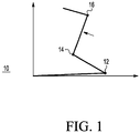
- FIG. 1 illustrates the typical behavior as a Transmission Line Pulse (TLP) curve of such an ESD protection device.
- TLP Transmission Line Pulse
- the operation of the ESD protection circuit is triggered in which the SCR becomes activated, causing a reduction in voltage across the ESD protection circuit.
- This reduction of the voltage is referred to as the "snapback voltage.” Therefore, after reaching the trigger voltage Vt1, the voltage drops towards the holding voltage Vh at point 14.
- the difference between the trigger voltage Vt and the holding voltage Vh is the snapback voltage Vsb. Subsequently, the ESD protection device is capable of conducting larger currents to protect the IC until the ESD protection device is damaged at point 16.
- the holding voltage be a particular amount to be able to provide latchup immunity.
- the higher the holding voltage a better quality and robustness can be achieved as it helps prevent against the risk of latchup.
- Current ESD protection circuits fail to provide a sufficiently high holding voltage, therefore a need exists for an improved ESD protection circuit.
- An ESD protection circuit includes a bi-directional SCR with double emitter regions at the positive terminal when combined with a PNP transistor.
- the double emitter regions in the SCR results in increasing the holding voltage which may allow for improved latchup immunity.
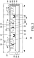
- FIG. 2 illustrates in cross-section form, an ESD protection circuit 300 (also referred to as semiconductor device 300) in accordance with one embodiment of the present invention.
- ESD protection circuit 300 also referred to as semiconductor device 300
- FIG. 2 illustrates in cross-section form, an ESD protection circuit 300 (also referred to as semiconductor device 300) in accordance with one embodiment of the present invention. Only a cross-sectional view is presented and the skilled person knows that it means that the structure extends for some distance in a direction perpendicular to the plane of the figure. Further, as will be discussed hereinafter, some of the structures enclose a region, which means that they extend for some distance in the direction perpendicular to the plane of the figure and subsequently follow a path parallel to the plane of the figure.
- Device 300 includes a p-doped substrate 302.
- P-doped substrate 302 has a first side 303.
- p-doped substrate 302 may also be subdivided in two layers.
- the bottom layer (seen in the orientation as presented in FIG. 2 ) is a p-doped semiconductor material on which a p-doped epitaxy layer has been manufactured.
- the p-doped semiconductor material should be comparable to the p-doped epitaxy layer.
- Substrate 302 is electrically brought into contact with a substrate voltage or a ground voltage via a substrate connection (not shown).
- An isolation structure is formed within substrate 302 to subdivide substrate 302 into a remaining portion and an isolated portion.
- the isolated portion is enclosed by the isolation structure.
- the isolation structure includes, at least, an N-buried layer NBL 338 which is arranged inside p-doped substrate 302 at a border between the isolated portion and the remaining portion. NBL 338 is arranged in a lateral direction and is arranged, seen from the first side, below the interface between the isolated portion and the remaining portion.
- the isolation structure also includes a Deep Trench Isolation structure DTI 332 and 350 which encloses the isolated portion. Note that DTI 332 and 350 are optional.
- the isolation structure also includes N-doped regions 334 and 348 which extend from the first side 303 towards NBL 338. N-doped regions 334 and 348 are adjacent to the Deep Trench Isolation structure, DTI 332 and 350, and enclose the isolated portion.
- a first N-doped region 340 and a second N-doped region 344 are formed in the isolated portion and extend from first side 303 towards NBL 338.
- First N-doped region 340 and second N-doped region 344 subdivide the isolated portion into a first portion pepi1 336, a second portion pepi2 342, and a third portion pepi3 346.
- First portion pepi1 336, second portion pepi2 342, and third portion pepi3 346 are non-overlapping with each other.
- a first p-doped well region 308, a second p-doped well region 316, and a third p-doped well region 324 are formed in the first portion 336, second portion 342, and third portion 346, respectively.
- Each of p-doped well regions 308, 316, and 324 may be referred to as p-doped regions.
- Each one of first p-doped region 308, second p-doped region 316, and third p-doped region 324 extend from first side 303 into its corresponding portion pepin 336, 342, and 346, respectively.
- P-doped regions 308, 316, and 324 do not extend completely to NBL 338.
- p-doped regions 308, 316, and 324 each have a p-dopant concentration which is higher than the p-dopant concentration of the respective first portion pepi1 336, second portion pepi2 342, and third portion pepi3 346.
- Shallow trench isolation (STI) regions 301 are also included at first side 303 between the p-doped regions.
- a first P contact region 306 is located within first p-doped region 308.
- P contact region 306 is connected to an electrical connection 304 which is connected to a negative voltage NEG terminal (or node) of device 300.
- NEG is generally tied to a ground voltage.
- P contact region 306 is a highly doped P+ region which has a higher p-dopant concentration than the p-dopant concentration of first p-doped region 308.
- N contact regions 314 and 312 and P contact region 310 are formed in second p-doped region 316, and an N contact region 322 and a P contact region 318 are formed in third p-doped region 324.
- N contact regions 314, 312, and 322 and P contact regions 310 and 318 extend from first side 303 into respective P-doped regions, however, they do not extend completely to the bottom of the respective P-doped regions. That is, as seen in a direction from the first side 303, contact regions 310, 314, 312, 318, and 322 are each surrounded by the respective p-doped region 316 or 324.
- the P contact regions 310 and 318 are highly doped P+ regions and have a p-dopant concentration which is higher than the p-dopant concentration of the P-doped regions 316 and 324.
- An electrical connection 362 is connected to each of N contact regions 312 and 314 and P contact region 310. Electrical connection 362 is configured to be connected to an I/O pad of the semiconductor device 300, referred to as the positive POS terminal (or node) of device 300.
- An electrical connection 360 is connected to N contact region 322 and P contact region 318. Electrical connection 360 is configured to be connected to NEG or to a ground voltage.
- the doped regions and contact regions may be formed in different orientations.
- N contact region 322 and P contact region 318 may be reversed such that N contact region 322 may be located on the left of P contact region 318.
- the contact regions in p-doped region 324 may be arranged differently.
- FIG. 2 schematically shows transistors NPN1 370, PNP1 372, NPN3 374, NPN2 376, and PNP2 378 of the circuit.
- NPN1 370 is formed by the n-p-n junctions from N contact region 322 to p-doped region 324 to NBL 338.
- PNP1 372 is formed by the p-n-p junctions from p-doped region 324 to N-doped region 344 to p-doped region 316.
- NPN3 374 is formed by the n-p-n junctions from N contact region 312 to p-doped region 316 to NBL 338.
- NPN2 376 is formed by the n-p-n junctions from N contact region 314 to p-doped region 316 to NBL 338.
- PNP2 is formed by the p-n-p junctions from p-doped region 316 to N-doped region 340 to p-doped region 308.
- Contact region 322 provides a contact to the emitter of NPN1 and contact region 318 provides a contact to the base of NPN1.
- Contact region 312 provides a contact to the emitter of NPN3 and contact region 314 provides a contact to the emitter of NPN2.
- Contact region 310 provides a contact to the base of NPN3 and NPN2.
- Electrical connection 362 electrically connects the emitters of NPN3 and NPN2 such that the combination of NPN3 and NPN2 form a double emitter device.
- an emitter of PNP1 is tied to the bases of NPN3 and NPN2, a base of PNP1 is tied to the collector of NPN1, and a collector of PNP 1 is tied to the base of NPN1.
- An emitter of PNP2 is tied to NEG, a base of PNP2 is tied to the collectors of NPN2 and NPN3, and the collector of PNP2 is tied to the bases of NPN3 and NPN2. Therefore, it can be seen that NPN1, PNP1, NPN3, and NPN2 form a first bi-directional SCR 380 having double emitters (i.e. emitters of both NPN3 and NPN2) on the POS terminal. Note that a second SCR 382 is formed by NPN3, NPN2, and PNP2.
- the voltage across the SCR1 380 increases towards a first trigger voltage Vt1 SCR1 380 starts to operate.
- Vt1 the current value through the ESD protection device 300 is equal to the trigger current It1.
- the first trigger voltage Vt1 strongly depends on a distance Sp (see FIG. 2 ) between N-doped region 344 and p-doped region 324 along a shortest line through the third portion pepi3 346.
- the distance Sp between N-doped region 344 and p-doped region 324 is configured to obtain a first predefined trigger voltage Vt1.
- the n-p junction from N-doped region 340 towards p-doped region 308 is reverse biased.
- the breakdown voltage of this junction is reached at the second trigger voltage Vt2
- an avalanche phenomenon by impact ionization is created through this n-p junction.
- a hole current flows through from p-doped region 308.
- the p-doped region is resistive and once the voltage difference between N-doped region 340 and the first p-doped region 308 becomes larger than 0.3 volt, transistor PNP2 starts to operate.
- the current through PNP2 increases with the voltage across PNP2.
- the second trigger voltage Vt2 strongly depends on a distance Spi2 ( FIG.
- the distance Spi2 between p-doped region 308 and N-doped region 340 is configured to obtain a first predefined trigger voltage Vt2.
- SCR1 380 is configured to have a first trigger voltage Vt1 which is larger than the second trigger voltage Vt2.
- Vt1 the second trigger voltage Vt2 is reached first when the voltage across ESD protection device 300 increases. Consequently PNP2 is switched on first and initially conducts away a current of the ESD event towards the NEG terminal. If, after the start of the operation of PNP2, the voltage across ESD protection device 300 still increases, the first trigger voltage Vt1 may be reached and SCR1 380 is also switched on to conduct more current of the ESD event towards the NEG terminal. This may result in snapback behavior. However, the snapback behavior is only observed at a snapback current Isb which is much higher than the trigger current It1 of SCR1 380.
- SCR1 380 includes two emitter regions contacted by contact 312 and 314 and a base region contacted by contact 310. Both emitter regions and the base region are connected to the POS terminal by way of electrical connection 362.
- the main current flow from base contact 310 at the POS terminal to the emitter contact 322 at the NEG terminal.
- the additional emitter region provided by NPN3 and contact 312 is in the main current flow.
- the n-p junction formed by contact 312 and P-doped region 316 would be reverse biased.
- This resulting higher field would modulate the forward current flow, resulting in a higher Vh than would be achievable with only a single emitter region of SCR 380 (i.e. with NPN2 but without NPN3).
- This higher holding voltage can allow device 300 to meet specifications which require a higher holding voltage than previously possible with prior art SCR devices. This may allow for improved latchup immunity.
- FIG. 4 illustrates, in cross-section form, an ESD protection circuit 400 in accordance with another embodiment of the present invention.
- a bi-directional SCR 402 is coupled in series with a bi-directional SCR 404 having a double emitter region, and a PNP transistor 405 coupled in parallel with SCR 404.
- SCR 402 may be an SCR as known in art, such as one having a single emitter region, and SCR 404 may be similar to SCR1 380 described above having a double emitter region formed by NPN3 374 and NPN2 376.
- Device 400 includes a substrate 406.
- P-doped substrate 406 has a first side 403.
- substrate 406 may also be subdivided in two layers.
- the bottom layer (seen in the orientation as presented in FIG. 4 ) is a p-doped semiconductor material on which a p-doped epitaxy layer has been manufactured.
- the p-doped semiconductor material should be comparable to the p-doped epitaxy layer.
- Substrate 406 is electrically brought into contact with a substrate voltage or a ground voltage via a substrate connection (not shown).
- a buried oxide layer (BOX) can be located between substrate 406 and the p-doped epitaxy layer. In this case, substrate 406 can be either n-type or p-type.
- An isolation structure is formed within substrate 406 to subdivide substrate 406 into a remaining portion and an isolated portion.
- the isolated portion is enclosed by the isolation structure.
- the isolation structure include, at least, a buried oxide layer BOX 409 which is arranged in a lateral direction inside p-doped substrate 406 at a border between the isolated portion and the remaining portion.
- the isolation structure also includes an N-buried layer NBL 407, arranged in a lateral direction, above BOX 409.
- the isolation structure also includes a Deep Trench Isolation structure DTI 418 and 422 which, along with BOX 409, enclose the isolated portion. Note that DTI 418, 420, and 422 are optional.
- the isolation structure also includes N-doped regions 480, 484, 486, 488, and 492 which extend from the first side 403 towards NBL 407.
- N-doped region 480 is adjacent to DTI 418 and N-doped regions 484 and 486 are adjacent to DTI 420. Note that if DTI 430 were not present, N-doped regions 484 and 486 could form a single N-doped region.
- N-doped region 492 is adjacent DTI 422.
- N-doped region 482, an N-doped region 488, and an N-doped region 490 are formed in the isolated portion and extend from first side 403 towards NBL 507.
- N-doped region 482, N-doped region 488, and N-doped region 490, along with N doped regions 484 and 486, subdivide the isolated portion into a first portion pepi1 408, a second portion pepi2 410, a third portion pepi3 412, a fourth portion pepi4 414, and a fifth portion pepi5 416.
- First portion pepi1 408, second portion pepi2 410, third portion pepi3 412, fourth portion pepi4 414, and fifth portion pepi5 416 are non-overlapping with each other.
- Isolation regions 426 are formed within NBL 407 at the bottom of first portion pepi1 408 such that NBL 407 is not continuous under first portion pepi1 408.
- a p-doped well region 428 and a p-doped well region 430 is formed in first portion 408, a p-doped well region 438 is formed in second portion 410, a p-doped well region 450 and a p-doped well region 448 is formed in third portion 412, a p-doped region 458 is formed in fourth portion 414, and a p-doped region 466 is formed in fifth portion 416.
- EAc of p-doped well regions 428, 430, 438, 450, and 448 may be referred to as p-doped regions.
- Each one of these p-doped regions extend from first side 403 into its corresponding portion pepin, respectively, and do not extend completely to the NBL 407.
- p-doped regions 428, 430, 438, 450, 448, 458, and 466 each have a p-dopant concentration which is higher than the p-dopant concentration of the respective first, second, third, fourth, and fifth portions.
- P-doped regions 430 and 428 may be considered portions of a same well, and p-doped regions 450 and 448 may be considered portions of a same well.
- P-doped regions 430 and 450 are high voltage well regions.
- Shallow trench isolation (STI) regions 401 are also included at first side 403 between the p-doped regions
- a P contact region 436 is located within p-doped region 430.
- An N contact region 434 and a P contact region 432 are located within p-doped region 428.
- P contact region 436 and N contact region 434 are connected to an electrical connection 470 which is connected to a negative voltage NEG terminal (or node) of device 400.
- NEG is generally tied to a ground voltage.
- N contact region N+ 442 and P contact region 440 are located in p-doped region 438.
- a P contact region 456 is located within p-doped region 450.
- An N contact region 454 and a P contact region 452 are located within p-doped region 448.
- N contact region 442, P contact region 440, P contact region 456, and N contact region 454 are connected to each other with an electrical connection 472.
- An N contact region 464, a P contact region 462, and an N contact region 460 are located in p-doped region 458.
- An electrical connection 474 is connected to each of N contact regions 464 and 460 and P contact region 462. Electrical connection 474 is configured to be connected to an I/O pad of the semiconductor device 400, referred to as the positive POS) terminal (or node) of device 400.
- a P contact region 468 is located in p-doped region 466 and is configured to be connected to NEG or to a ground voltage.
- P contact regions are highly doped P+ regions and have a p-dopant concentration that is higher than the p-dopant concentration of p-doped regions 428, 438, 448, 458, and 466.
- the N contact regions are highly doped N+ regions which have a higher dopant concentration than N-doped regions 480, 482, 484, 486, 488, 490, and 492.
- the doped regions and contact regions may be formed in different orientations. Similarly, the contact regions may be arranged differently.
- FIG. 5 schematically shows transistors NPN1' 504, PNP1' 506, NPN2' 508, NPN1 510, PNP1 512, NPN3 514, NPN2 516, and PNP2 518 of the circuit. These transistors are relevant for a situation in which an ESD event is received.
- the corresponding circuit diagram of the electrical circuit implemented in the semiconductor device 400 in case that an ESD event (either forward or reverse ESD event) is received, is presented in FIG. 5 .
- NPN1' 504 is formed by the n-p-n junctions from N contact region 434 to p-doped region 428 to NBL 407.
- PNP1' 506 is formed by the p-n-p junctions from p-doped region 428 to N-doped region 482 to p-doped region 438.
- NPN2' 508 is formed by the n-p-n junction from N contact region 442 to p-doped region 438 to NBL 407.
- NPN1 510 is formed by the n-p-n junctions from N contact region 454 to p-doped region 448 to NBL 407.
- PNP1 512 is formed by the p-n-p junctions from p-doped region 448 to N-doped region 488 to p-doped region 458.
- NPN3 514 is formed by the n-p-n junctions from N contact region 464 to p-doped region 458 to NBL 407.
- NPN2 516 is formed by the n-p-n junctions from N contact region 460 to p-doped region 458 to NBL 407.
- PNP2 is formed by the p-n-p junctions from p-doped region 458 to N-doped region 490 to p-doped region 466.
- Contact region 436 provides a contact to the base of NPN1' 504 and contact region 434 provides a contact to the emitter of NPN1' 504.
- Contact region 442 provides a contact to the emitter of NPN2' 508 and contact region 440 provides a contact to the base of NPN2' 508.
- Contact region 456 provides a contact to the base of NPN1 510 and contact region 454 provides a contact to the emitter of NPN1 510.
- Contact region 464 provides a contact to the emitter of NPN3 514, contact region 460 provides a contact to the emitter of NPN2 516, and contact region 462 provides a contact to the base of NPN3 514 and NPN2 526.
- Electrical connection 474 electrically connects the emitters of NPN3 514 and NPN2 516 such that the combination of NPN3 and NPN2 form a double emitter device.
- an emitter of PNP1' is tied to the base of NPN2', a base of PNP1' is tied to the collectors of NPN1' and NPN2', and a collector of PNP1' is tied to the base of NPN1'.
- the base of NPN1' and the emitter of NPN1' are tied to the NEG terminal.
- An emitter of NPN2', the base of NPN2', the base of NPN1, and the emitter of NPN1 are all tied together.
- An emitter of PNP1 is tied to the bases of NPN3 and NPN2, a base of PNP1 is tied to the collector of NPN1, and a collector of PNP 1 is tied to the base of NPN1.
- NPN1, PNP1, NPN3, and NPN2 form a first bi-directional SCR 404 having double emitters (i.e. emitters of both NPN3 and NPN2) on the POS terminal.
- a second SCR 402 is formed by NPN1', PNP1', and NPN2'.
- a third SCR 502 is formed by NPN3, NPN2, and PNP2.
- SCR1 404 includes two emitter regions contacted by contact 464 and 460 and a base region contacted by contact 462. Both emitter regions and the base region are connected to the POS terminal by way of electrical connection 474.
- the main current flow is from base contact 462 at the POS terminal to emitter contact 454 at the NEG terminal and through SCR 404.
- the additional emitter region provided by NPN3 and contact 464 is therefore in the main current flow.
- an SCR device with a double emitter region may allow for an increased holding voltage for an ESD protection device.
- This increased holding voltage as compared to prior art ESD protection circuits, improves latchup immunity.
- a higher holding voltage helps ensure that the holding voltage is greater than any normal operating voltage in the integrated circuit. This results in an ESD protection device that is more robust in that it prevents against the risk of latchup until higher operating voltages.
- Coupled is not intended to be limited to a direct coupling or a mechanical coupling.
- an electrostatic discharge (ESD) protection device includes a first bi-directional silicon controlled rectifier (SCR) which includes a substrate; a first doped well in the substrate, the first doped well having a first conductivity type; a buried doped layer in the substrate, the buried doped layer having a second conductivity type opposite the first conductivity type; first and second highly doped regions of the second conductivity type in the first doped well; a third highly doped region of the first conductivity type in the first doped well, wherein the first, second and third highly doped regions are connected to a first node; a first transistor in the first doped well, the first transistor including an emitter coupled to the first highly doped region, a collector coupled to a first conductive line in the buried doped layer, and a base coupled to the third highly doped region; a second transistor in the first doped well, the second transistor including an emitter coupled to the second highly doped region, a collector coupled to the first conductive line in the buried doped layer, and
- the first SCR further includes a first doped substrate region having the second conductivity type; a second doped well in the substrate, the second doped well having the first conductivity type; a fourth highly doped region of the first conductivity type in the second doped well; a third transistor in the first doped substrate region, the third transistor including a first emitter connected to the third highly doped region, a base coupled to the first conductive line and a second emitter connected to the fourth highly doped region.
- the first SCR further includes a third doped well in the substrate, the third doped well having the first conductivity type; a fifth highly doped region of the second conductivity type in the third doped well; a sixth highly doped region of the first conductivity type in the third doped well, wherein the fifth and sixth highly doped regions are connected to a second node; a fourth transistor in the third doped well, the fourth transistor including an emitter coupled to the fifth highly doped region, a collector coupled to the first conductive line in the buried doped layer, and a base coupled to the sixth highly doped region.
- the first SCR further includes a second doped substrate region having the second conductivity type; a fifth transistor in the second doped substrate region, the fifth transistor including a first emitter connected to the third highly doped region, a base coupled to the first conductive line and a second emitter connected to the sixth highly doped region and the base of the base of the fourth transistor.
- the ESD protection device further includes a second SCR including a fourth doped well in the substrate, the fourth doped well having the first conductivity type; a seventh highly doped region of the second conductivity type in the fourth doped well; an eighth highly doped region of the first conductivity type in the fourth doped well, wherein the seventh and eighth highly doped regions are connected to a third node; a sixth transistor in the fourth doped well, the sixth transistor including an emitter coupled to the seventh highly doped region, a collector coupled to a second conductive line in the buried doped layer, and a base coupled to the eighth highly doped region.
- a second SCR including a fourth doped well in the substrate, the fourth doped well having the first conductivity type; a seventh highly doped region of the second conductivity type in the fourth doped well; an eighth highly doped region of the first conductivity type in the fourth doped well, wherein the seventh and eighth highly doped regions are connected to a third node; a sixth transistor in the fourth doped well, the sixth transistor
- the second SCR further includes a fifth doped well in the substrate, the fifth doped well having the first conductivity type; a ninth highly doped region of the second conductivity type in the fifth doped well; a tenth highly doped region of the first conductivity type in the fifth doped well, wherein the ninth and tenth highly doped regions are connected to the second node; a seventh transistor in the fifth doped well, the seventh transistor including an emitter coupled to the tenth highly doped region, a collector coupled to the second conductive line in the buried doped layer, and a base coupled to the tenth highly doped region.
- the second SCR further includes a third doped substrate region having the second conductivity type; an eighth transistor in the third doped substrate region, the eighth transistor including a first emitter coupled to the eighth highly doped region, a second emitter coupled to the ninth highly doped region, and a base coupled to the second conductive line.
- the ESD protection device further includes a portion of the fourth doped well that includes the eighth highly doped region is a high voltage doped well; and a portion of the third doped well that includes the sixth highly doped region is a high voltage doped well.
- the ESD protection device further includes an isolation region in the buried layer below the fourth doped well.
- the ESD protection device further includes a portion of the first, second, third, fourth and fifth doped wells is a doped epitaxial layer.
- an electrostatic discharge (ESD) protection device in another embodiment, includes a first bi-directional silicon controlled rectifier in a semiconductor substrate that includes a first doped well of a first conductivity type; a first transistor in the first doped well that has an emitter connected to a first electrode of a second conductivity type, a collector coupled to a doped buried region of the second conductivity type, and a base connected to a second electrode of the first conductivity type; a second transistor in the first doped well that has an emitter connected to a third electrode of the second conductivity type, a collector coupled to the doped buried region, and a base connected to the second electrode, wherein the first, second and third electrodes are in the first doped well; a first doped substrate region of the second conductivity type adjacent the first doped well; a second doped well of the first conductivity type; and a third transistor in the first doped substrate region that has a first emitter connected to the second electrode, a base coupled to the doped buried region, and a second emit
- the ESD protection device further includes a fourth transistor in the second doped well, the second transistor including an emitter connected to a fifth electrode of the second conductivity type, a collector connected to the doped buried region, and a base connected to the fourth electrode, wherein the fifth electrode is in the second doped well.
- the ESD protection device further includes a first node, wherein the first, second and third electrodes are connected to the first node.
- the ESD protection device further includes a second node, wherein the fourth and fifth electrodes are connected to the second node.
- when the first node is biased high with reference to the second node current flows from the second electrode to the fifth electrode.
- the ESD protection device further includes a second bi-directional silicon controlled rectifier in the semiconductor substrate that includes: a third doped well of the first conductivity type; a third node; a fifth transistor in the third doped well that has an emitter connected to a sixth electrode of the second conductivity type, a collector connected to the doped buried region, and a base connected to a seventh electrode of the first conductivity type, wherein the sixth and seventh electrodes are in the third doped well and are connected to the third node.
- a second bi-directional silicon controlled rectifier in the semiconductor substrate that includes: a third doped well of the first conductivity type; a third node; a fifth transistor in the third doped well that has an emitter connected to a sixth electrode of the second conductivity type, a collector connected to the doped buried region, and a base connected to a seventh electrode of the first conductivity type, wherein the sixth and seventh electrodes are in the third doped well and are connected to the third node.
- the second bi-directional silicon controlled rectifier further includes: a second doped substrate region of the second conductivity type adjacent the third doped well; a fourth doped well of the first conductivity type; a sixth transistor in the second doped substrate region that has a first emitter connected to the seventh electrode, a base coupled to the doped buried region, and a second emitter connected to an eighth electrode of the second conductivity type, wherein the eighth electrode is in the fourth doped well and the doped buried region is below the second doped substrate region and the third and fourth doped wells.
- the second bi-directional silicon controlled rectifier further includes: a seventh transistor in the fourth doped well that has an emitter connected to a ninth electrode of the first conductivity type, a collector connected to the doped buried region, and a base connected to the eighth electrode, wherein the eighth and ninth electrodes are connected to the second node.
- the ESD protection device further includes a fifth doped well of the first conductivity type; a third doped substrate region of the second conductivity type between the first doped well and the fifth doped well; an eighth transistor in the third doped substrate region that has a first emitter connected to the second electrode, a base coupled to the doped buried region, and a second emitter connected to an eighth electrode of the second conductivity type, wherein the eighth electrode is in the fifth doped well and the doped buried region is below the second doped substrate region and the third and fourth doped wells.
- the first conductivity type is p-type conductivity
- the second conductivity type is n-type conductivity
- the first node is a positive node
- the second and third nodes are negative nodes.
Landscapes
- Semiconductor Integrated Circuits (AREA)
- Bipolar Integrated Circuits (AREA)
Priority Applications (3)
| Application Number | Priority Date | Filing Date | Title |
|---|---|---|---|
| EP17306137.5A EP3451379A1 (de) | 2017-09-01 | 2017-09-01 | Schutzschaltung gegen elektrostatische entladung mit einem bidirektionalen gesteuerten silicium-gleichrichter (scr) |
| US16/038,852 US10497696B2 (en) | 2017-09-01 | 2018-07-18 | Electrostatic discharge protection circuit with a bi-directional silicon controlled rectifier (SCR) |
| CN201811013410.4A CN109427770B (zh) | 2017-09-01 | 2018-08-31 | 具有双向硅控整流器(scr)的静电放电保护电路 |
Applications Claiming Priority (1)
| Application Number | Priority Date | Filing Date | Title |
|---|---|---|---|
| EP17306137.5A EP3451379A1 (de) | 2017-09-01 | 2017-09-01 | Schutzschaltung gegen elektrostatische entladung mit einem bidirektionalen gesteuerten silicium-gleichrichter (scr) |
Publications (1)
| Publication Number | Publication Date |
|---|---|
| EP3451379A1 true EP3451379A1 (de) | 2019-03-06 |
Family
ID=59846537
Family Applications (1)
| Application Number | Title | Priority Date | Filing Date |
|---|---|---|---|
| EP17306137.5A Withdrawn EP3451379A1 (de) | 2017-09-01 | 2017-09-01 | Schutzschaltung gegen elektrostatische entladung mit einem bidirektionalen gesteuerten silicium-gleichrichter (scr) |
Country Status (3)
| Country | Link |
|---|---|
| US (1) | US10497696B2 (de) |
| EP (1) | EP3451379A1 (de) |
| CN (1) | CN109427770B (de) |
Cited By (3)
| Publication number | Priority date | Publication date | Assignee | Title |
|---|---|---|---|---|
| CN110600466A (zh) * | 2019-09-03 | 2019-12-20 | 捷捷半导体有限公司 | 一种基于可控硅原理的双向可编程过压保护器件 |
| CN112928111A (zh) * | 2021-01-27 | 2021-06-08 | 深圳市国微电子有限公司 | 耐正负高压的scr esd防护器件及其工艺方法 |
| CN114975420A (zh) * | 2021-02-23 | 2022-08-30 | 力晶积成电子制造股份有限公司 | 双向可控硅整流器 |
Families Citing this family (4)
| Publication number | Priority date | Publication date | Assignee | Title |
|---|---|---|---|---|
| CN110690270B (zh) * | 2019-10-12 | 2023-03-14 | 上海华力微电子有限公司 | 一种内嵌硅控整流器的pmos器件及其实现方法 |
| CN110867487B (zh) * | 2019-11-28 | 2024-01-05 | 上海华力微电子有限公司 | 硅控整流器及其制造方法 |
| US11611211B2 (en) | 2021-04-19 | 2023-03-21 | Analog Devices, Inc. | Multiple trigger electrostatic discharge (ESD) protection device for integrated circuits with multiple power supply domains |
| CN116454080B (zh) * | 2022-01-10 | 2024-05-14 | 长鑫存储技术有限公司 | 静电保护结构及静电保护电路 |
Citations (3)
| Publication number | Priority date | Publication date | Assignee | Title |
|---|---|---|---|---|
| WO2011144960A1 (en) * | 2010-05-18 | 2011-11-24 | Freescale Semiconductor, Inc. | Integrated circuit, electronic device and esd protection therefor |
| US20130032882A1 (en) * | 2011-08-04 | 2013-02-07 | Analog Devices, Inc. | Bi-directional blocking voltage protection devices and methods of forming the same |
| US20140111892A1 (en) * | 2012-10-23 | 2014-04-24 | Macronix International Co., Ltd. | Bi-directional bipolar junction transistor for high voltage electrostatic discharge protection |
Family Cites Families (8)
| Publication number | Priority date | Publication date | Assignee | Title |
|---|---|---|---|---|
| US7342281B2 (en) * | 2004-12-14 | 2008-03-11 | Electronics And Telecommunications Research Institute | Electrostatic discharge protection circuit using triple welled silicon controlled rectifier |
| US20090273006A1 (en) * | 2008-04-30 | 2009-11-05 | Wen-Yi Chen | Bidirectional silicon-controlled rectifier |
| US8653557B2 (en) * | 2010-02-22 | 2014-02-18 | Sofics Bvba | High holding voltage electrostatic discharge (ESD) device |
| US8946822B2 (en) * | 2012-03-19 | 2015-02-03 | Analog Devices, Inc. | Apparatus and method for protection of precision mixed-signal electronic circuits |
| US9620495B2 (en) | 2012-09-12 | 2017-04-11 | Nxp Usa, Inc. | Semiconductor device and an integrated circuit comprising an ESD protection device, ESD protection devices and a method of manufacturing the semiconductor device |
| US9659922B2 (en) * | 2013-06-13 | 2017-05-23 | Nxp Usa, Inc. | ESD protection device |
| US10014289B2 (en) * | 2013-11-22 | 2018-07-03 | Nxp Usa, Inc. | Electrostatic discharge protection circuits and structures and methods of manufacture |
| US9287255B2 (en) | 2014-07-09 | 2016-03-15 | Freescale Semiconductor Inc. | ESD protection device and related fabrication methods |
-
2017
- 2017-09-01 EP EP17306137.5A patent/EP3451379A1/de not_active Withdrawn
-
2018
- 2018-07-18 US US16/038,852 patent/US10497696B2/en active Active
- 2018-08-31 CN CN201811013410.4A patent/CN109427770B/zh active Active
Patent Citations (3)
| Publication number | Priority date | Publication date | Assignee | Title |
|---|---|---|---|---|
| WO2011144960A1 (en) * | 2010-05-18 | 2011-11-24 | Freescale Semiconductor, Inc. | Integrated circuit, electronic device and esd protection therefor |
| US20130032882A1 (en) * | 2011-08-04 | 2013-02-07 | Analog Devices, Inc. | Bi-directional blocking voltage protection devices and methods of forming the same |
| US20140111892A1 (en) * | 2012-10-23 | 2014-04-24 | Macronix International Co., Ltd. | Bi-directional bipolar junction transistor for high voltage electrostatic discharge protection |
Cited By (5)
| Publication number | Priority date | Publication date | Assignee | Title |
|---|---|---|---|---|
| CN110600466A (zh) * | 2019-09-03 | 2019-12-20 | 捷捷半导体有限公司 | 一种基于可控硅原理的双向可编程过压保护器件 |
| CN112928111A (zh) * | 2021-01-27 | 2021-06-08 | 深圳市国微电子有限公司 | 耐正负高压的scr esd防护器件及其工艺方法 |
| CN112928111B (zh) * | 2021-01-27 | 2022-08-09 | 深圳市国微电子有限公司 | 耐正负高压的scr esd防护器件及其工艺方法 |
| CN114975420A (zh) * | 2021-02-23 | 2022-08-30 | 力晶积成电子制造股份有限公司 | 双向可控硅整流器 |
| CN114975420B (zh) * | 2021-02-23 | 2025-05-02 | 力晶积成电子制造股份有限公司 | 双向可控硅整流器 |
Also Published As
| Publication number | Publication date |
|---|---|
| CN109427770A (zh) | 2019-03-05 |
| US10497696B2 (en) | 2019-12-03 |
| CN109427770B (zh) | 2023-09-12 |
| US20190074275A1 (en) | 2019-03-07 |
Similar Documents
| Publication | Publication Date | Title |
|---|---|---|
| US10497696B2 (en) | Electrostatic discharge protection circuit with a bi-directional silicon controlled rectifier (SCR) | |
| US10361185B2 (en) | ESD protection device with buried layer having variable doping concentrations | |
| US9620495B2 (en) | Semiconductor device and an integrated circuit comprising an ESD protection device, ESD protection devices and a method of manufacturing the semiconductor device | |
| US7868387B2 (en) | Low leakage protection device | |
| US9209265B2 (en) | ESD devices comprising semiconductor fins | |
| CN110364523B (zh) | Esd保护装置、包括esd保护装置的半导体装置和其制造方法 | |
| US9431389B2 (en) | ESD transistor for high voltage and ESD protection circuit thereof | |
| CN108520875B (zh) | 一种高维持电压npnpn型双向可控硅静电防护器件 | |
| US9461032B1 (en) | Bipolar ESD protection device with integrated negative strike diode | |
| CN103427408B (zh) | 用于高电压应用的静电放电保护 | |
| CN105655325A (zh) | 静电放电保护电路、结构及其制造方法 | |
| CN107799517B (zh) | 用于半导体结构的esd装置 | |
| TW200532887A (en) | ESD protection device for high voltage and negative voltage tolerance | |
| US9443841B2 (en) | Electrostatic discharge protection structure capable of preventing latch-up issue caused by unexpected noise | |
| US9142545B2 (en) | Electrostatic discharge protection structure capable of preventing latch-up issue caused by unexpected noise | |
| CN105322935A (zh) | 智能半导体开关 | |
| US9960251B2 (en) | ESD protection structure and method of fabrication thereof | |
| CN110120390B (zh) | 半导体设备及其构造方法 | |
| KR100750588B1 (ko) | 정전기 방전 보호회로 | |
| CN112447703A (zh) | 静电放电防护元件 | |
| KR20180058432A (ko) | 정전기 방전 보호회로 | |
| JP2014038922A (ja) | 半導体装置 | |
| JP2000232203A (ja) | ラテラルバイポーラ型入出力保護装置 | |
| CN107046022A (zh) | 静电放电保护器件和集成电路 |
Legal Events
| Date | Code | Title | Description |
|---|---|---|---|
| PUAI | Public reference made under article 153(3) epc to a published international application that has entered the european phase |
Free format text: ORIGINAL CODE: 0009012 |
|
| STAA | Information on the status of an ep patent application or granted ep patent |
Free format text: STATUS: THE APPLICATION HAS BEEN PUBLISHED |
|
| AK | Designated contracting states |
Kind code of ref document: A1 Designated state(s): AL AT BE BG CH CY CZ DE DK EE ES FI FR GB GR HR HU IE IS IT LI LT LU LV MC MK MT NL NO PL PT RO RS SE SI SK SM TR |
|
| AX | Request for extension of the european patent |
Extension state: BA ME |
|
| STAA | Information on the status of an ep patent application or granted ep patent |
Free format text: STATUS: REQUEST FOR EXAMINATION WAS MADE |
|
| 17P | Request for examination filed |
Effective date: 20190906 |
|
| RBV | Designated contracting states (corrected) |
Designated state(s): AL AT BE BG CH CY CZ DE DK EE ES FI FR GB GR HR HU IE IS IT LI LT LU LV MC MK MT NL NO PL PT RO RS SE SI SK SM TR |
|
| STAA | Information on the status of an ep patent application or granted ep patent |
Free format text: STATUS: EXAMINATION IS IN PROGRESS |
|
| 17Q | First examination report despatched |
Effective date: 20200526 |
|
| STAA | Information on the status of an ep patent application or granted ep patent |
Free format text: STATUS: THE APPLICATION HAS BEEN WITHDRAWN |
|
| 18W | Application withdrawn |
Effective date: 20200814 |