EP3452168B1 - Behandlungsanordnung und verfahren zur herstellung einer behandlungsanordnung - Google Patents
Behandlungsanordnung und verfahren zur herstellung einer behandlungsanordnung Download PDFInfo
- Publication number
- EP3452168B1 EP3452168B1 EP17713151.3A EP17713151A EP3452168B1 EP 3452168 B1 EP3452168 B1 EP 3452168B1 EP 17713151 A EP17713151 A EP 17713151A EP 3452168 B1 EP3452168 B1 EP 3452168B1
- Authority
- EP
- European Patent Office
- Prior art keywords
- treatment
- arrangement
- electrode
- shielding layer
- plastics
- Prior art date
- Legal status (The legal status is an assumption and is not a legal conclusion. Google has not performed a legal analysis and makes no representation as to the accuracy of the status listed.)
- Active
Links
Images



Classifications
-
- A—HUMAN NECESSITIES
- A61—MEDICAL OR VETERINARY SCIENCE; HYGIENE
- A61N—ELECTROTHERAPY; MAGNETOTHERAPY; RADIATION THERAPY; ULTRASOUND THERAPY
- A61N1/00—Electrotherapy; Circuits therefor
- A61N1/44—Applying ionised fluids
-
- A—HUMAN NECESSITIES
- A61—MEDICAL OR VETERINARY SCIENCE; HYGIENE
- A61F—FILTERS IMPLANTABLE INTO BLOOD VESSELS; PROSTHESES; DEVICES PROVIDING PATENCY TO, OR PREVENTING COLLAPSING OF, TUBULAR STRUCTURES OF THE BODY, e.g. STENTS; ORTHOPAEDIC, NURSING OR CONTRACEPTIVE DEVICES; FOMENTATION; TREATMENT OR PROTECTION OF EYES OR EARS; BANDAGES, DRESSINGS OR ABSORBENT PADS; FIRST-AID KITS
- A61F13/00—Bandages or dressings; Absorbent pads
- A61F13/00051—Accessories for dressings
-
- A—HUMAN NECESSITIES
- A61—MEDICAL OR VETERINARY SCIENCE; HYGIENE
- A61N—ELECTROTHERAPY; MAGNETOTHERAPY; RADIATION THERAPY; ULTRASOUND THERAPY
- A61N1/00—Electrotherapy; Circuits therefor
- A61N1/02—Details
- A61N1/04—Electrodes
- A61N1/0404—Electrodes for external use
- A61N1/0408—Use-related aspects
- A61N1/0468—Specially adapted for promoting wound healing
-
- A—HUMAN NECESSITIES
- A61—MEDICAL OR VETERINARY SCIENCE; HYGIENE
- A61N—ELECTROTHERAPY; MAGNETOTHERAPY; RADIATION THERAPY; ULTRASOUND THERAPY
- A61N1/00—Electrotherapy; Circuits therefor
- A61N1/02—Details
- A61N1/04—Electrodes
- A61N1/0404—Electrodes for external use
- A61N1/0472—Structure-related aspects
- A61N1/0492—Patch electrodes
-
- A—HUMAN NECESSITIES
- A61—MEDICAL OR VETERINARY SCIENCE; HYGIENE
- A61N—ELECTROTHERAPY; MAGNETOTHERAPY; RADIATION THERAPY; ULTRASOUND THERAPY
- A61N1/00—Electrotherapy; Circuits therefor
- A61N1/40—Applying electric fields by inductive or capacitive coupling ; Applying radio-frequency signals
-
- H—ELECTRICITY
- H05—ELECTRIC TECHNIQUES NOT OTHERWISE PROVIDED FOR
- H05H—PLASMA TECHNIQUE; PRODUCTION OF ACCELERATED ELECTRICALLY-CHARGED PARTICLES OR OF NEUTRONS; PRODUCTION OR ACCELERATION OF NEUTRAL MOLECULAR OR ATOMIC BEAMS
- H05H1/00—Generating plasma; Handling plasma
- H05H1/24—Generating plasma
- H05H1/2406—Generating plasma using dielectric barrier discharges, i.e. with a dielectric interposed between the electrodes
-
- H—ELECTRICITY
- H05—ELECTRIC TECHNIQUES NOT OTHERWISE PROVIDED FOR
- H05H—PLASMA TECHNIQUE; PRODUCTION OF ACCELERATED ELECTRICALLY-CHARGED PARTICLES OR OF NEUTRONS; PRODUCTION OR ACCELERATION OF NEUTRAL MOLECULAR OR ATOMIC BEAMS
- H05H1/00—Generating plasma; Handling plasma
- H05H1/24—Generating plasma
- H05H1/2406—Generating plasma using dielectric barrier discharges, i.e. with a dielectric interposed between the electrodes
- H05H1/2418—Generating plasma using dielectric barrier discharges, i.e. with a dielectric interposed between the electrodes the electrodes being embedded in the dielectric
-
- A—HUMAN NECESSITIES
- A61—MEDICAL OR VETERINARY SCIENCE; HYGIENE
- A61F—FILTERS IMPLANTABLE INTO BLOOD VESSELS; PROSTHESES; DEVICES PROVIDING PATENCY TO, OR PREVENTING COLLAPSING OF, TUBULAR STRUCTURES OF THE BODY, e.g. STENTS; ORTHOPAEDIC, NURSING OR CONTRACEPTIVE DEVICES; FOMENTATION; TREATMENT OR PROTECTION OF EYES OR EARS; BANDAGES, DRESSINGS OR ABSORBENT PADS; FIRST-AID KITS
- A61F13/00—Bandages or dressings; Absorbent pads
- A61F2013/00361—Plasters
- A61F2013/00902—Plasters containing means
- A61F2013/00919—Plasters containing means for physical therapy, e.g. cold or magnetic
-
- H—ELECTRICITY
- H05—ELECTRIC TECHNIQUES NOT OTHERWISE PROVIDED FOR
- H05H—PLASMA TECHNIQUE; PRODUCTION OF ACCELERATED ELECTRICALLY-CHARGED PARTICLES OR OF NEUTRONS; PRODUCTION OR ACCELERATION OF NEUTRAL MOLECULAR OR ATOMIC BEAMS
- H05H2277/00—Applications of particle accelerators
- H05H2277/10—Medical devices
Definitions
- the invention relates to a treatment arrangement for treating a surface, with a flat electrode arrangement to which an electrical voltage can be supplied and a flat shielding layer consisting of an insulating plastic which at least partially surrounds the electrode arrangement, the electrode arrangement consisting of a plastic provided with conductive additives.
- the invention further relates to a treatment device with such a treatment arrangement and a method for producing a treatment arrangement of the type mentioned.
- Various treatment arrangements are known with which a surface can be treated under the action of electrical voltages. These include treatment arrangements in which a current is introduced directly into the surface to be treated.
- the shielding layer has the function of avoiding an operator touching the electrode.
- the shielding layer serves to isolate the electrode from the surface to be treated, in order to prevent direct current introduction and possibly the formation of arcing sparks.
- the treatment arrangement is designed as a plasma treatment device and is used to build up a high-voltage field by means of the electrode arrangement by ionizing an air or gas space between the treatment arrangement and the surface to be treated to a plasma, so that a known one Plasma treatment of the surface takes place.
- the electrode arrangement can have one pole of an electrical voltage are connected and the surface to be treated form a counter electrode.
- the surface to be treated can be a material which is prepared by the treatment, for example a plasma treatment, on its surface for being provided with a layer, for example a protective layer.
- the treatment of the surface then serves to improve the adhesion of the layer in the manner of a primer treatment.
- Such treatments are suitable for materials made of plastic, metal, wood or the like.
- a preferred application in the context of the invention is the treatment of human or animal skin as the surface to be treated.
- the plasma treatment has a disinfectant, ie germicidal effect.
- the layer of the treatment arrangement facing the wound can be formed from silicone, which is known to be skin-friendly and skin-friendly and is suitable as an insulating layer.
- a suitable material is, for example, the silicone gel SILPURAN® from Wacker Chemie AG, Burghausen, Germany. This two-component silicone gel cross-links to form a soft silicone layer that has a certain stickiness and therefore adheres to the skin.
- a metallic electrode is completely embedded in a dielectric, which can be a silicone.
- the dielectric can be provided with through-openings through which the wound secretions are made can pass from the wound side of the treatment arrangement to the distal side, where it can be absorbed, for example, by an absorption material.
- the embedded electrode must be provided with corresponding through openings, the diameter of which, however, is larger than the diameter of the through openings in the dielectric, so that the dielectric reliably covers the electrode also in the region of the channels formed by the through openings.
- the electrode embedded in the dielectric has a flat and flexible single-pole design, so that the body belonging to the skin surface acts as a counter electrode.
- the counter electrode can be grounded or act as a "floating electrode".
- the structure of the known treatment arrangements has proven itself, since both the dielectric and the electrode itself can be designed flexibly, and thus the entire treatment arrangement is suitable for adapting to the possibly irregular shape of a part of the body and thus treating an intact skin surface or a wound defined distance ratios and thus reproducible results.
- US 2012/0213664 A1 discloses a treatment arrangement for a plasma treatment, with the container or the like designed as a foil bag or bottle. can be treated.
- the treatment arrangement has two electrodes, the electrode facing the article to be treated having interruptions as a flat ground electrode through which the plasma field can extend in order to generate a surface plasma.
- a flexible dielectric is located between the electrodes.
- the dielectric forms a flexible wall with the high-voltage electrode on the inside and the interrupted ground electrode on the outside, which wall can adapt to the shape of an object, for example a bottle.
- the wall is connected to a base body of the dielectric via a cavity.
- the electrodes applied to the surfaces of the flexible wall can consist of a conductive silicone polymer. None is disclosed about the connection of the electrodes to the dielectric wall.
- the treatment arrangement is obviously not intended for the treatment of human or animal skin or wound areas.
- WO 2012/106735 A2 discloses various designs of treatment arrangements in which a conductive electrode is embedded in a flat, flexible dielectric.
- a conductive electrode is embedded in a flat, flexible dielectric.
- a face mask it is proposed to form a first dielectric layer in a negative shape corresponding to the face, to apply a conductive electrode layer there, which is enclosed with a further dielectric layer.
- the electrically conductive layer are a conductive ink, a metal foil or a conductive gel. A separate connection of the conductive layer with the dielectric is not disclosed.
- the present invention has for its object to simplify the structure of a treatment arrangement of the type mentioned and to make it even more reliable.
- a treatment arrangement of the type mentioned at the outset is characterized in that in the region of the boundary layer between the electrode arrangement and the shielding layer, the plastics of the electrode arrangement and the shielding layer are materially bonded to one another without an additional adhesive layer in that the plastics are mixed with one another in the region of the boundary layer and / or are networked with one another.
- an electrode is therefore not at least partially surrounded, in particular completely embedded, with the dielectric plastic layer as a metallic electrode, but rather is completely embedded, but the electrode itself is formed from a suitable plastic which is made conductive by additives.
- Such electrodes are known per se. According to the invention, they are used to form the treatment arrangement so as to enable a material connection between the electrode arrangement and the shielding layer, which results from the plastics themselves and has no additional adhesive layer at the boundary layer between the electrode arrangement and the shielding layer.
- the electrode arrangement and the shielding layer can thus be designed as a single material and thus ensure a high level of security against delamination of the electrode arrangement from the shielding layer. This is particularly important if the treatment arrangement is advantageously flexible and allows strong bends to be able to adapt even to difficult parts of the body, for example to be able to wrap around a wrist.
- the material-locking connection according to the invention between the plastic of the electrode arrangement and the plastic of the shielding layer succeeds after a mixture of these plastics, at least in the area of the boundary layer, if the plastics - at least in this area - harden and / or crosslink together.
- chemically identical plastics are used for the electrode arrangement and the shielding layer, which can thereby be mixed well.
- the plastic is only provided with the conductive additives, which can be metallic particles, for example micro- or nanoparticles, graphite powder or the like.
- the plastics of the electrode arrangement and the shielding layer which abut one another in the boundary layer.
- This can be done in that a first of the plastics is initially only partially cross-linked and is further cross-linked with the second of the plastics when it is cross-linked in the sense of the original cross-linking.
- the first of the plastics can also be completely crosslinked if it has functional crosslinkable marginal groups which, when the uncrosslinked second of the plastics are fed in, lead to a secondary crosslinking between the first plastic and the second plastic.
- the electrode arrangement is enclosed on all sides by the shielding layer. This is particularly advantageous if a high voltage is supplied to the electrode, as is the case for treatment with a dielectric barrier plasma in a preferred embodiment of the invention.
- the shielding layer is profiled on the treatment side to form contact surfaces, between which the air gaps exist to form the plasma when the treatment arrangement is applied to the surface to be treated.
- the profiling can be irregular or regular.
- EP 2 515 997 A1 a profiling in the form of round knobs is known from DE 10 2013 019 057 A1 also in the form of chambers open on one side, which are formed on the treatment side of the shielding layer and can optionally be filled with nourishing or healing substances.
- a wound dressing surface is formed on the treatment side. This can be formed by the suitable material of the shielding layer itself or additionally applied to the treatment side of the shielding layer.
- silicones in any form are suitable for the shielding layer and the electrode arrangement.
- An embodiment of the treatment arrangement according to the invention is particularly suitable for the purpose of wound care, in which the shielding layer has portions which protrude beyond the surface of the electrode and are designed to be adhesive to the surface to be treated. If necessary, the adhesive property of a silicone gel itself can be used for this. In this case, the silicone layer can already secure the entire arrangement on the skin in the vicinity of the wound, so that it may be attached to one Secondary dressing can be dispensed with in addition to the treatment arrangement.
- a single-pole electrode can be used as the electrode arrangement of a treatment arrangement according to the invention if the surface to be treated or the body located behind it functions as a counter electrode.
- the electrode arrangement can be at least two-pole, the two poles being connected to the poles of a voltage supply.
- the electrodes are then expediently shaped and positioned in such a way that in many areas over the surface of the treatment arrangement the electrode of one pole runs close and parallel to the electrode of the other pole, so that a spatial electric field suitable for plasma formation is created between these two poles.
- the two electrode poles are preferably designed in the form of strips and guided parallel or antiparallel over the surface of the treatment arrangement. Meander shapes, spiral courses, comb-shaped structures etc. are suitable for this.
- a treatment device is preferably formed, which is designed and positioned to change direct contact between the electrode arrangement and the surface to be treated.
- a treatment device is preferably formed, which is designed and positioned to change direct contact between the electrode arrangement and the surface to be treated.
- the material connection according to the invention can be produced between the plastic of the electrode arrangement and the plastic of the shielding layer in that the plastics are mixed with one another in a liquid state and cured and / or crosslinked together at least in the area of an interface between the electrode arrangement and the shielding layer. In this way, the material closure is brought about by a uniform matrix structure or a gradual transition from one matrix structure to the other matrix structure.
- At least one layer of the shielding layer and then the plastic of the electrode arrangement provided with the conductive additives, in each case in a liquid state, is introduced into a casting mold, so that mixing occurs in the border area between the plastics, and then the plastics can be cured and / or crosslinked together by cooling.
- the possible crosslinking for example in the case of a silicone gel, can take place by means of a crosslinking component which leads to crosslinking in a temperature-dependent or temperature-independent manner.
- the electrode arrangement or the shielding layer is first molded and partially cross-linked with the plastic.
- the other plastic can then be injected into a mold, for example an injection mold, and brought to crosslinking, the second plastic being selected such that the first plastic, which is initially only partially crosslinked, is crosslinked.
- the first plastic can be inserted as a preformed part in an injection mold, which is used to shape the second plastic, which is supplied in the uncrosslinked liquid state.
- the second plastic is chosen so that it creates a secondary crosslinking with the crosslinkable groups of the first plastic part.
- this is possible through OH groups, which allow a polycondensation reaction with elimination of water.
- Another example arises with residual reactive SiH groups that enable additive crosslinking with reactive vinyl groups of the other silicone plastic.
- all other polymerization reactions are also suitable for secondary crosslinking.
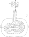
- the Figures 1 and 2 illustrate a treatment arrangement in which a dielectric shielding layer 1, in which an electrode arrangement 2 is embedded such that the shielding layer 1 surrounds the electrode arrangement 2 on all sides.
- the shielding layer 1 is formed with a thickness such that the electrode arrangement 2 is surrounded on all sides with a sufficiently thick dielectric shield that prevents a noticeable current flow.
- the shielding layer 1 forms a lateral connecting tongue 3, into which the electrode arrangement 2 extends.
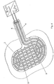
- the electrode arrangement 2 has two electrode strips 4, which run as strip-shaped conductors parallel to one another and are spirally wound in an oval shape, inner ends 5 being terminated in straight pieces pointing antiparallel in a loop of the other electrode strip.
- the two electrode strips run parallel to one another and end in contact surfaces 6, which are connected to a pole 8 of a high-voltage supply device 9 via connecting lines 7.
- Figure 1 is schematically illustrated that an AC voltage is present at one pole, which oscillates around a ground potential, while the other pole 8 is at the ground potential.
- the electrode arrangement 2 is thus supplied with an alternating high voltage.
- the two electrode strips 4 are arranged in such a way that they always alternate with one another in parallel sections, so that the alternating high voltage of the high-voltage supply device 9 is always present between the sections of the electrode strips lying parallel to one another and generate local electric fields there, which form a dielectric barrier plasma are suitable.
- the dielectric shielding layer 1 is provided in one piece with sections 10, which extend on all sides - with the exception of the connecting tongue 3 - over the electrode arrangement 2 and the shielding layer 1 embedding the electrode arrangement 2 and are designed to be adhesive on their underside 11, so that the treatment arrangement with the other Underside 11 adhesive sections 10 can be attached to the skin of a body part in the manner of a plaster.
- Figure 2 illustrates the smaller thickness of the sections 10 compared to the remaining shielding layer 1, which embeds the electrode arrangement 2 in the form of the electrode strips 4 on all sides.
- the dielectric shielding layer 1 is provided outside the electrode strips 4 with through openings 12, through which air can reach a wound surface on the one hand and wound secretion from a wound surface on the other, from the underside of the shielding layer 1 forming a treatment side 13 to the distal upper side 14 is transportable.
- the electrode arrangement 2 is a flat arrangement with a small height extension, which is formed in this embodiment of the invention by the flat electrode strips.
- These are preferably formed from an electrically conductive silicone by means of conductive additives, which corresponds to the silicone from which the dielectric shielding layer 1 is made.
- Figure 3 only illustrates that the two poles 8 of the high-voltage supply device can both be connected to alternating alternating voltages, which have a phase shift of 180 ° with respect to one another, so that the resulting voltage difference for forming the local electric fields between the electrode strips 4 has a double amplitude.
- the second exemplary embodiment shown differs from the first exemplary embodiment according to FIGS Figures 1 to 4 only in that the treatment side 13 of the dielectric shielding layer 1 is not smooth, but has a profile 15 in the form of hemispherical elevations, with the tops of which the treatment arrangement can rest on the surface to be treated, in particular on the skin of a part of the body.
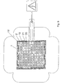
- the exemplary embodiment shown has an essentially square surface of the dielectric shielding layer 1, to which sections 10 'are connected in one piece like a cloverleaf.
- the electrode arrangement 2 ' is formed by a continuously electrically conductive surface in which there are circular through openings 18.
- the electrically conductive surface of the electrode arrangement 2 ' is embedded on all sides in the dielectric shielding layer 1.
- Through-openings 12 of the dielectric shielding layer run concentrically with the through-openings 18, the diameter of which, however, is significantly smaller than the diameter of the through-openings 18 in the electrode arrangement 2 '. This ensures that sufficient insulation to the electrode arrangement 2 ′ is always present in the area of the through openings 12, which ensure ventilation of the wound area and removal of wound secretions.
- the dielectric shielding layer 1 also has a connecting tongue 3 ', into which a corresponding extension of the electrode arrangement 2' extends, the electrode arrangement 2 'also being completely shielded on all sides by the dielectric shielding layer 1 in the region of the connecting tongue 3'.
- Contact is made via a contact point 19, via which a high-voltage potential of the high-voltage supply device 9 is conducted to the electrode arrangement 2 '.
- the body of the surface to be treated forms a counter electrode for the alternating high voltage of the high voltage supply device 9.
- the bottom view according to Figure 9 illustrates a profile 15 'of the treatment side 13 of the dielectric shielding layer 1.
- the profile 15' is formed with lattice-like walls 20, which around the through openings 12, 18 to the surface to be treated open chambers 21 ( Figure 8 ) in which, as in the air gaps 17 of the previous embodiments, a plasma can form when the treatment arrangement rests on the skin or wound surface of a body.
- the electrode arrangements 2, 2 'and the shielding layers 1 consist of chemically essentially the same plastics as so-called liquid silicone rubbers or silicone gels. These plastic materials are insulating as a plastic matrix.
- conductive additives are admixed to the insulating plastic material, so that the required conductive configuration of the electrode arrangements 2, 2' is made possible despite the use of the insulating plastic matrix. In this way, a connection between the electrode arrangement 2, 2 ′ and the dielectric shielding layer 1, which is secure against delamination even when the flexible treatment arrangement is severely deformed, is achieved.
Landscapes
- Health & Medical Sciences (AREA)
- Engineering & Computer Science (AREA)
- Public Health (AREA)
- Biomedical Technology (AREA)
- Veterinary Medicine (AREA)
- Life Sciences & Earth Sciences (AREA)
- Animal Behavior & Ethology (AREA)
- General Health & Medical Sciences (AREA)
- Physics & Mathematics (AREA)
- Plasma & Fusion (AREA)
- Radiology & Medical Imaging (AREA)
- Nuclear Medicine, Radiotherapy & Molecular Imaging (AREA)
- Spectroscopy & Molecular Physics (AREA)
- Heart & Thoracic Surgery (AREA)
- Vascular Medicine (AREA)
- Electrotherapy Devices (AREA)
- Plasma Technology (AREA)
- Shielding Devices Or Components To Electric Or Magnetic Fields (AREA)
- Physical Or Chemical Processes And Apparatus (AREA)
- Treatments Of Macromolecular Shaped Articles (AREA)
- Materials For Medical Uses (AREA)
- Liquid Crystal (AREA)
Description
- Die Erfindung betrifft eine Behandlungsanordnung zur Behandlung einer Oberfläche, mit einer flächigen Elektrodenanordnung, der eine elektrische Spannung zuführbar ist, und einer flächigen, aus einem isolierenden Kunststoff bestehenden Abschirmschicht, die die Elektrodenanordnung zumindest teilweise umgibt wobei die Elektrodenanordnung aus einem leitfähigen Zusätzen versehenen Kunststoff besteht.
- Die Erfindung betrifft ferner eine Behandlungsvorrichtung mit einer derartigen Behandlungsanordnung sowie ein Verfahren zur Herstellung einer Behandlungsanordnung der erwähnten Art.
- Es sind verschiedene Behandlungsanordnungen bekannt, mit denen eine Oberfläche unter der Einwirkung elektrischer Spannungen behandelt werden können. Hierzu gehören Behandlungsanordnungen, bei denen ein Strom unmittelbar in die zu behandelnde Oberfläche eingeleitet wird. Die Abschirmschicht hat dabei die Funktion, eine Berührung der Elektrode durch eine Bedienperson zu vermeiden.
- Ferner ist es bekannt, mittels der Elektrode eine induktive Erwärmung der zu behandelnden Oberfläche vorzunehmen. In diesem Fall dient die Abschirmschicht der Isolierung der Elektrode gegenüber der zu behandelnden Oberfläche, um eine direkte Stromeinleitung und gegebenenfalls die Ausbildung von Überschlagsfunken zu verhindern.
- In einer bevorzugten Ausführung der erfindungsgemäßen Behandlungsanordnung ist diese als Plasma-Behandlungsvorrichtung ausgebildet und dient dazu, mittels der Elektrodenanordnung ein Hochspannungsfeld aufzubauen, indem ein Luft- oder Gasraum zwischen der Behandlungsanordnung und der zu behandelnden Oberfläche zu einem Plasma ionisiert wird, sodass eine an sich bekannte Plasmabehandlung der Oberfläche erfolgt. Dabei kann im Rahmen der vorliegenden Erfindung die Elektrodenanordnung mit einem Pol einer elektrischen Spannung verbunden werden und die zu behandelnde Oberfläche eine Gegenelektrode bilden. Es ist aber auch möglich, die Elektrodenanordnung aus wenigstens zwei Elektroden zu bilden, die mit unterschiedlichen Polen einer elektrischen Spannung verbunden sind, sodass zwischen den Elektroden ein elektrisches Feld aufgebaut wird, mit dem beispielsweise Luft zur Ausbildung eines Plasmas ionisiert werden kann.
- Die zu behandelnde Oberfläche kann ein Material sein, das durch die Behandlung, beispielsweise einer Plasmabehandlung, an seiner Oberfläche dazu vorbereitet wird, mit einer Schicht, beispielsweise einer Schutzschicht, versehen zu werden. Die Behandlung der Oberfläche dient dann dazu, die Haftung der Schicht nach Art einer Grundierungsbehandlung zu verbessern. Derartige Behandlungen kommen für Materialien aus Kunststoff, Metall, Holz o. dgl. in Frage.
- Eine im Rahmen der Erfindung bevorzugte Anwendung ist die Behandlung der menschlichen oder tierischen Haut als zu behandelnde Oberfläche. Insbesondere für die Ausbildung eines Plasmas sind vorteilhafte Effekte auf die Hautoberfläche nachgewiesen worden. Insbesondere hat die Plasmabehandlung eine desinfizierende, also keimtötende Wirkung. Es ist daher bekannt, eine Behandlungsanordnung für eine Plasmabehandlung in Form einer Wundauflage auszubilden. Die der Wunde zugekehrte Schicht der Behandlungsanordnung kann dabei aus Silikon gebildet sein, das bekanntlich hautfreundlich und hautverträglich ist und als isolierenden Schicht geeignet ist. Ein in Frage kommendes Material ist beispielsweise das Silikongel SILPURAN® der Wacker Chemie AG, Burghausen, Deutschland. Dieses Zwei-Komponenten-Silikongel vernetzt zu einer weichen Silikonschicht, die eine gewisse Klebrigkeit aufweist und daher auf der Haut haftet.
- In Frage kommende Formen derartiger Behandlungsanordnungen sind beispielsweise durch
DE 10 2014 013 716 A1 bekannt und für die Behandlung der Haut beziehungsweise von Wunden mit einem dielektrisch behinderten Plasma bekannt. Dabei ist eine metallische Elektrode vollständig in einem Dielektrikum, das ein Silikon sein kann, eingebettet. Um den Abfluss von Wundsekret zu ermöglichen, kann das Dielektrikum mit Durchgangsöffnungen versehen sein, durch die Wundsekret von der Wundseite der Behandlungsanordnung auf die distale Seite hindurch treten kann, wo es beispielsweise von einem Absorptionsmaterial aufgenommen werden kann. Die eingebettete Elektrode muss dabei mit entsprechenden Durchgangsöffnungen versehen sein, deren Durchmesser allerdings größer ist als der Durchmesser der Durchgangsöffnungen in dem Dielektrikum, sodass das Dielektrikum die Elektrode auch im Bereich der durch die Durchgangsöffnungen gebildeten Kanäle zuverlässig abdeckt. Die in dem Dielektrikum eingebettete Elektrode ist dabei flächig und flexibel einpolig ausgebildet, sodass der zu der Hautoberfläche gehörende Körper als Gegenelektrode fungiert. Die Gegenelektrode kann dabei geerdet sein oder als "floatende Elektrode" wirken. Der Aufbau der bekannten Behandlungsanordnungen hat sich bewährt, da sowohl das Dielektrikum als auch die Elektrode selbst flexibel ausgebildet werden können und somit die gesamte Behandlungsanordnung dafür geeignet ist, sich der gegebenenfalls unregelmäßigen Form eines Körperteils anzupassen und so die Behandlung einer unversehrten Hautoberfläche oder einer Wunde mit definierten Abstandsverhältnissen und somit reproduzierbaren Ergebnissen durchzuführen. -
US 2012/0213664 A1 offenbart eine Behandlungsanordnung für eine Plasmabehandlung, mit der als Folienbeutel oder Flasche ausgebildete Behälter für Lebensmittel o.dgl. behandelt werden können. Die Behandlungsanordnung weist zwei Elektroden auf, wobei die dem zu behandelnden Artikel zugewandte Elektrode als flächige Masseelektrode Unterbrechungen aufweist, durch die sich das Plasmafeld zur Erzeugung eines Oberflächenplasmas erstrecken kann. Zwischen den Elektroden befindet sich ein flexibles Dielektrikum. In einem Ausführungsbeispiel bildet das Dielektrikum mit der Hochspannungselektrode auf einer Innenseite und der unterbrochenen Masseelektrode auf der Außenseite eine flexible Wandung, die sich an die Form eines Gegenstands, beispielsweise einer Flasche, anpassen kann. Hierzu ist die Wandung über einen Hohlraum mit einem Grundkörper des Dielektrikums verbunden. Die auf die Oberflächen der flexiblen Wandung aufgebrachten Elektroden können aus einem leitenden Silikonpolymer bestehen. Über die Verbindung der Elektroden mit der dielektrischen Wandung ist nichts offenbart. Die Behandlungsanordnung ist ersichtlich nicht für die Behandlung der menschlischen oder tierischen Haut oder von Wundflächen vorgesehen. -
WO 2012/106735 A2 offenbart verschiedene Ausbildungen von Behandlungsanordnungen, bei denen eine leitende Elektrode in einem flächigen flexiblen Dielektrikum eingebettet ist. Für das Ausführungsbeispiel einer Gesichtsmaske wird vorgeschlagen, eine erste Dielektrikumschicht in einer dem Gesicht entsprechenden Negativform auszubilden, dort eine leitende Elektrodenschicht aufzubringen, die mit einer weiteren dielektrischen Schicht eingeschlossen wird. Beispiele für die elektrisch leitende Schicht ist eine leitende Tinte, eine Metallfolie oder ein leitendes Gel. Eine eigene Verbindung der leitenden Schicht mit dem Dielektrikum ist nicht offenbart. - Der vorliegenden Erfindung liegt die Aufgabe zugrunde, den Aufbau einer Behandlungsanordnung der eingangs erwähnten Art zu vereinfachen und noch zuverlässiger zu gestalten.
- Zur Lösung dieser Aufgabe ist erfindungsgemäß eine Behandlungsanordnung der eingangs erwähnten Art dadurch gekennzeichnet, dass im Bereich der Grenzschicht zwischen Elektrodenanordnung und Abschirmschicht die Kunststoffe der Elektrodenanordnung und der Abschirmschicht ohne eine zusätzliche Klebschicht materialschlüssig dadurch miteinander verbunden sind, dass die Kunststoffe im Bereich der Grenzschicht miteinander gemischt und/oder miteinander vernetzt sind.
- Bei der erfindungsgemäßen Behandlungsanordnung wird somit eine Elektrode nicht als metallische Elektrode mit der dielektrischen Kunststoffschicht zumindest teilweise umgeben, insbesondere vollständig eingebettet, sondern die Elektrode wird selbst aus einem geeigneten Kunststoff ausgebildet, der durch Zusätze leitfähig gemacht wird. Derartige Elektroden sind an sich bekannt. Erfindungsgemäß werden sie zur Ausbildung der Behandlungsanordnung eingesetzt, um so eine materialschlüssige Verbindung zwischen der Elektrodenanordnung und der Abschirmschicht zu ermöglichen, die sich durch die Kunststoffe selbst ergibt und keine zusätzliche Klebschicht an der Grenzschicht zwischen der Elektrodenanordnung und der Abschirmschicht aufweist. Elektrodenanordnung und Abschirmschicht können somit quasi als einheitliches Material ausgebildet werden und gewähren dadurch eine hohe Sicherheit gegen eine Delaminierung der Elektrodenanordnung von der Abschirmschicht. Dies ist insbesondere von Bedeutung, wenn die Behandlungsanordnung in vorteilhafter Weise flexibel ist und starke Biegungen ermöglicht, um sich auch schwierigen Körperteilen anpassen zu können, also beispielsweise ein Handgelenk umschlingen können.
- Die erfindungsgemäße materialschlüssige Verbindung zwischen dem Kunststoff der Elektrodenanordnung und dem Kunststoff der Abschirmschicht gelingt nach einer Mischung dieser Kunststoffe zumindest im Bereich der Grenzschicht in einfacher Weise, wenn die Kunststoffe - zumindest in diesem Bereich - gemeinsam aushärten und/oder vernetzen. In einer weiter bevorzugten Ausführungsform werden für die Elektrodenanordnung und die Abschirmschicht chemisch gleiche Kunststoffe verwendet, die sich dadurch gut mischen lassen. Für die Elektrodenanordnung ist der Kunststoff dabei lediglich mit den leitfähigen Zusätzen versehen, die metallische Teilchen, beispielsweise Mikro- oder Nanoteilchen, Graphitpulver o. ä. sein können.
- Alternativ ist es möglich, auf die Mischung der Kunststoffe zu verzichten und die materialschlüssige Verbindung dadurch herzustellen, dass die in der Grenzschicht aneinanderstoßenden Kunststoffe von Elektrodenanordnung und Abschirmschicht miteinander vernetzen. Dies kann dadurch geschehen, dass ein erster der Kunststoffe zunächst nur teilvernetzt wird und mit dem zweiten der Kunststoffe bei dessen Vernetzung im Sinne der ursprünglichen Vernetzung weitervernetzt wird. In einer anderen Ausführungsform kann der erste der Kunststoffe auch vollständig vernetzt werden, wenn er funktionelle vernetzbare randständige Gruppen aufweist, die bei Zuführung des unvernetzten zweiten der Kunststoffe bei dessen Vernetzung zu einer Sekundärvernetzung zwischen dem ersten Kunststoff und dem zweiten Kunststoff führen.
- In einer bevorzugten Ausführungsform der Erfindung ist die Elektrodenanordnung allseitig von der Abschirmschicht umschlossen. Dies ist insbesondere vorteilhaft, wenn der Elektrode eine Hochspannung zugeführt wird, wie dies für die Behandlung mit einem dielektrisch behinderten Plasma in einer bevorzugten Ausführungsform der Erfindung der Fall ist.
- In dieser Konfiguration ist es möglich, einen elektrisch leitenden Anschluss der Elektrodenanordnung aus der Abschirmschicht herauszuführen. Alternativ ist es möglich, die Elektrodenanordnung beispielsweise mit einer Anschlusszunge, die ebenfalls von der Abschirmschicht umschlossen ist, auszubilden und die elektrische Spannung mit einer Kontaktanordnung zuzuführen, die die Abschirmschicht durchstößt und dadurch den Kontakt zur Elektrodenanordnung herstellt. Eine derartige Kontaktierung mit einem selbstschneidenden Kontakt ist beispielsweise durch
EP 2 723 447 B1 bekannt. - Auch für die erfindungsgemäße Behandlungsanordnung kann es zweckmäßig sein, wenn die Abschirmschicht auf der Behandlungsseite zur Ausbildung von Anlageflächen profiliert ist, zwischen denen bei Anlage der Behandlungsanordnung an der zu behandelnden Oberfläche die Luftzwischenräume zur Ausbildung des Plasmas bestehen. Dabei kann die Profilierung unregelmäßig oder regelmäßig sein. Aus
EP 2 515 997 A1 ist eine Profilierung in Form von runden Noppen bekannt, ausDE 10 2013 019 057 A1 auch in Form von einseitig offenen Kammern, die auf der Behandlungsseite der Abschirmschicht ausgebildet sind und gegebenenfalls mit pflegenden oder heilenden Substanzen gefüllt werden können. - Für die Anwendung als Wundbehandlungsanordnung ist es zweckmäßig, wenn auf der Behandlungsseite eine Wundauflagenfläche ausgebildet ist. Diese kann durch das geeignete Material der Abschirmschicht selbst gebildet sein oder auf die Behandlungsseite der Abschirmschicht ergänzend aufgebracht sein.
- Für die Abschirmschicht und die Elektrodenanordnung eignen sich insbesondere Silikone in jeder Form, bevorzugt in Form von Silikongelen.
- Insbesondere für den Zweck der Wundversorgung eignet sich eine Ausführungsform der erfindungsgemäßen Behandlungsanordnung, bei der die Abschirmschicht über die Fläche der Elektrode hinausragende Abschnitte aufweist, die zur zu behandelnden Oberfläche hin klebend ausgebildet sind. Gegebenenfalls kann hierfür die klebende Eigenschaft eines Silikongels selbst ausgenutzt werden. In diesem Fall kann die Silikonschicht bereits die Befestigung der gesamten Anordnung auf der Haut in der Umgebung der Wunde bewirken, sodass gegebenenfalls auf einen Sekundärverband zusätzlich zu der Behandlungsanordnung verzichtet werden kann.
- Als Elektrodenanordnung einer erfindungsgemäßen Behandlungsanordnung kann eine einpolige Elektrode verwendet werden, wenn die zu behandelnde Fläche beziehungsweise der dahinter befindliche Körper als Gegenelektrode fungiert. Alternativ kann die Elektrodenanordnung wenigstens zweipolig ausgebildet sein, wobei die beiden Pole mit den Polen einer Spannungsversorgung verbunden werden. Die Elektroden sind dann zweckmäßigerweise so geformt und positioniert, dass über die Fläche der Behandlungsanordnung in vielen Bereichen die Elektrode des einen Pols nahe und parallel zu der Elektrode des anderen Pols verläuft, sodass zwischen diesen beiden Polen ein für die Plasmabildung geeignetes räumliches elektrisches Feld entsteht. Damit das elektrische Feld über die Fläche verteilt und nicht nur lokal vorhanden ist, werden die beiden Elektrodenpole vorzugsweise streifenförmig ausgebildet und über die Fläche der Behandlungsanordnung parallel oder antiparallel geführt. Hierbei eignen sich Mäanderformen, spiralförmige Verläufe, kammförmige Strukturen usw.
- Mit einer erfindungsgemäßen Behandlungsanordnung wird bevorzugt eine Behandlungsvorrichtung gebildet, die zur Veränderung eines direkten Kontakts der Elektrodenanordnung und der zu behandelnden Oberfläche ausgebildet und positioniert ist. Wie bereits erläutert, kann es sich insbesondere für eine dielektrisch behinderte Plasmabehandlung anbieten, die Elektrodenanordnung vollständig in der elektrischen Abschirmschicht einzubetten.
- Die Herstellung des erfindungsgemäßen Materialschlusses zwischen dem Kunststoff der Elektrodenanordnung und dem Kunststoff der Abschirmschicht gelingt dadurch, dass zumindest im Bereich einer Grenzfläche zwischen der Elektrodenanordnung und der Abschirmschicht die Kunststoffe in einem flüssigen Zustand miteinander vermischt und gemeinsam ausgehärtet und/oder vernetzt werden. Auf diese Weise wird der Materialschluss durch eine einheitliche Matrixstruktur oder einen allmählichen Übergang von einer Matrixstruktur auf die andere Matrixstruktur bewirkt.
- Es ist durchaus möglich, die Elektrodenanordnung und/oder die Abschirmschicht vorzufertigen und teilweise oder ganz zu vernetzen oder auszuhärten und anschließend im Bereich einer Grenzfläche zu verflüssigen oder zumindest aufzuquellen, um so eine gemeinsame Aushärtung und/oder Vernetzung in diesem Bereich zu erreichen.
- Bevorzugt ist jedoch, dass in eine Gießform zunächst wenigstens eine Lage der Abschirmschicht und dann der mit den leitfähigen Zusätzen versehende Kunststoff der Elektrodenanordnung, jeweils in flüssigem Zustand, eingebracht wird, sodass sich im Grenzbereich zwischen den Kunststoffen eine Vermischung ergibt, und dass anschließend die Kunststoffe gemeinsam durch Abkühlung ausgehärtet und/oder vernetzt werden. Dabei kann die etwaige Vernetzung, beispielsweise bei einem Silikongel, durch eine Vernetzungskomponente erfolgen, die temperaturabhängig oder temperaturunabhängig zur Vernetzung führt.
- Auf die Vermischung der Kunststoffe im Grenzbereich kann im Falle der Vernetzung der Kunststoffe miteinander verzichtet werden. Hierfür kann vorgesehen werden, dass die Elektrodenanordnung oder die Abschirmschicht zunächst mit dem Kunststoff geformt und teilvernetzt wird. In einer Form, beispielsweise einer Spritzgussform, kann dann der andere Kunststoff eingespritzt und zur Vernetzung gebracht werden, wobei der zweite Kunststoff so gewählt ist, dass dabei der erste, zunächst nur teilvernetzte Kunststoff weitervernetzt wird.
- Alternativ hierzu ist es möglich, den ersten Kunststoff praktisch vollständig zu vernetzen und dabei mit funktionellen, vernetzbaren Gruppen zu versehen. Dabei kann der erste Kunststoff als vorgeformtes Teil in eine Spritzgussform eingelegt werden, mit der die Formung des zweiten Kunststoffs erfolgt, der im unvernetzten flüssigen Zustand zugeführt wird. Der zweite Kunststoff wird dabei so gewählt, dass er mit den vernetzbaren Gruppen des ersten Kunststoffteils eine Sekundärvernetzung herstellt. Insbesondere bei Silikonen ist dies durch OH-Gruppen möglich, die eine Polykondensationsreaktion unter Abspaltung von Wasser erlauben. Ein anderes Beispiel ergibt sich mit restlichen reaktiven SiH-Gruppen, die eine additive Vernetzung mit reaktiven Vinylgruppen des anderen Silikonkunststoffes ermöglichen. Für die Sekundärvernetzung sind aber auch alle anderen Polymerisationsreaktionen geeignet.
- Die Erfindung soll im Folgenden anhand von in der Zeichnung dargestellten Ausführungsbeispielen näher erläutert werden. Es zeigen:
- Figur 1 -
- eine Draufsicht auf ein erstes Ausführungsbeispiel einer erfindungsgemäßen Behandlungsanordnung, die an eine Spannungsversorgungseinrichtung angeschlossen ist;
- Figur 2 -
- einen Schnitt durch die Behandlungsanordnung gemäß
Figur 1 entlang der Linie A-A; - Figur 3 -
- das Ausführungsbeispiel gemäß
Figur 1 einer Behandlungsanordnung, die an eine modifizierte Spannungsversorgungseinrichtung angeschlossen ist; - Figur 4 -
- die Anordnung gemäß
Figur 3 in einer Darstellung zur Verdeutlichung der Elektrodenanordnung; - Figur 5 -
- eine Draufsicht auf ein zweites Ausführungsbeispiel einer erfindungsgemäßen Behandlungsanordnung;
- Figur 6 -
- einen Schnitt durch die Behandlungsanordnung gemäß
Figur 5 entlang der Linie B-B; - Figur 7 -
- eine Draufsicht auf eine dritte Ausführungsform einer erfindungsgemäßen Behandlungsanordnung, die an einen Pol einer Hochspannungsversorgungseinrichtung angeschlossen ist;
- Figur 8 -
- einen Schnitt durch die Behandlungsanordnung gemäß
Figur 7 ; - Figur 9 -
- eine Ansicht von unten auf die Behandlungsanordnung gemäß
Figur 7 . - Die
Figuren 1 und 2 illustrieren eine Behandlungsanordnung, in der eine dielektrische Abschirmschicht 1, in die eine Elektrodenanordnung 2 so eingebettet ist, dass die Abschirmschicht 1 die Elektrodenanordnung 2 allseitig umgibt. Hierzu ist die Abschirmschicht 1 mit einer solchen Dicke ausgebildet, dass die Elektrodenanordnung 2 allseitig mit einer ausreichend dicken dielektrischen Abschirmung umgeben ist, die einen merkbaren Stromfluss verhindert. Die Abschirmschicht 1 bildet eine seitliche Anschlusszunge 3 aus, in die sich die Elektrodenanordnung 2 erstreckt. - Wie insbesondere
Figur 4 erkennen lässt, weist die Elektrodenanordnung 2 zwei Elektrodenstreifen 4 auf, die als streifenförmige Leiter parallel zueinander verlaufen und in einer ovalen Form spiralförmig gewunden sind, wobei innere Enden 5 in antiparallel zeigenden geraden Stücken in jeweils einer Schleife des anderen Elektrodenstreifens abgeschlossen sind. In der Anschlusszunge 3 verlaufen die beiden Elektrodenstreifen parallel zueinander und enden in Kontaktflächen 6, die über Verbindungsleitungen 7 mit jeweils einem Pol 8 einer Hochspannungsversorgungseinrichtung 9 verbunden sind. InFigur 1 ist schematisch verdeutlicht, dass an einem Pol eine Wechselspannung anliegt, die um ein Massepotential herum oszilliert, während der andere Pol 8 auf dem Massepotential liegt. Die Elektrodenanordnung 2 wird somit mit einer alternierenden Wechsel-Hochspannung versorgt. Die beiden Elektrodenstreifen 4 sind so angeordnet, dass sie immer mit parallel verlaufenden Abschnitten miteinander abwechseln, sodass die Wechsel-hochspannung der Hochspannungsversorgungseinrichtung 9 immer zwischen den parallel zueinander liegenden Abschnitten der Elektrodenstreifen anliegt und dort lokale elektrische Felder erzeugen, die zur Ausbildung eines dielektrisch behinderten Plasmas geeignet sind. - Die dielektrische Abschirmschicht 1 ist einstückig mit Abschnitten 10 versehen, die sich allseitig - mit Ausnahme der Anschlusszunge 3 - über die Elektrodenanordnung 2 und die die Elektrodenanordnung 2 einbettende Abschirmschicht 1 erstrecken und an ihrer Unterseite 11 klebend ausgebildet sind, sodass die Behandlungsanordnung mit den an der Unterseite 11 klebenden Abschnitten 10 auf der Haut eines Körperteils nach Art eines Pflasters befestigt werden kann.
-
Figur 2 verdeutlicht die geringere Dicke der Abschnitte 10 gegenüber der übrigen Abschirmschicht 1, die die Elektrodenanordnung 2 in Form der Elektrodenstreifen 4 allseitig einbettet. - Die
Figuren 1 und 2 lassen noch erkennen, dass die dielektrische Abschirmschicht 1 außerhalb der Elektrodenstreifen 4 mit Durchgangsöffnungen 12 versehen ist, über die einerseits Luft an eine Wundfläche gelangen kann und andererseits von einer Wundfläche Wundsekret von der eine Behandlungsseite 13 bildenden Unterseite der Abschirmschicht 1 auf die distal liegende Oberseite 14 transportierbar ist. - Wie
Figur 1 verdeutlicht, befinden sich die Durchgangsöffnungen in den Zwischenräumen zwischen den Elektrodenstreifen 4, sodass die Isolation der Elektrodenanordnung 2 durch die Durchgangsöffnungen nicht gefährdet ist. -
Figur 2 lässt darüber hinaus erkennen, dass die Elektrodenanordnung 2 eine flächige Anordnung mit einer geringen Höhenerstreckung ist, die sich in dieser Ausführungsform der Erfindung durch die flachen Elektrodenstreifen bildet. Diese sind vorzugsweise aus einem durch leitende Zusätze elektrisch leitfähigen Silikon gebildet, das dem Silikon entspricht, aus dem die dielektrische Abschirmschicht 1 besteht. -
Figur 3 verdeutlicht lediglich, dass die beiden Pole 8 der Hochspannungsversorgungseinrichtung beide an alternierende Wechselspannungen angeschlossen sein können, die zueinander eine Phasenverschiebung von 180 ° aufweisen, sodass die resultierende Spannungsdifferenz zur Ausbildung der lokalen elektrischen Felder zwischen den Elektrodenstreifen 4 eine doppelte Amplitude aufweisen. - Das in den
Figuren 5 und 6 dargestellte zweite Ausführungsbeispiel unterscheidet sich von dem ersten Ausführungsbeispiel gemäß denFiguren 1 bis 4 lediglich dadurch, dass die Behandlungsseite 13 der dielektrischen Abschirmschicht 1 nicht glatt ausgebildet ist, sondern eine Profilierung 15 in Form von halbkugelförmigen Erhebungen aufweist, mit deren Oberseiten die Behandlungsanordnung auf der zu behandelnden Oberfläche, also insbesondere auf der Haut eines Körperteils, aufliegen kann. Zwischen den Auflageflächen 16' befinden sich Luftzwischenräume 17, in denen sich ein Plasma durch die zwischen den Elektrodenstreifen 4 aufgebauten elektrischen Felder bilden kann, wenn die Behandlungsanordnung auf der Haut eines Körperteils aufliegt. - Das in den
Figuren 7 bis 9 dargestellte Ausführungsbeispiel weist eine im Wesentlichen quadratische Fläche der dielektrischen Abschirmschicht 1 auf, an die sich einstückig Abschnitte 10' kleeblattartig anschließen. Die Elektrodenanordnung 2' ist durch eine durchgehend elektrisch leitende Fläche gebildet, in der sich kreisförmige Durchgangsöffnungen 18 befinden. Die elektrisch leitende Fläche der Elektrodenanordnung 2' ist allseitig in die dielektrische Abschirmschicht 1 eingebettet. Konzentrisch mit den Durchgangsöffnungen 18 verlaufen Durchgangsöffnungen 12 der dielektrischen Abschirmschicht, deren Durchmesser jedoch deutlich kleiner ist als der Durchmesser der Durchgangsöffnungen 18 in der Elektrodenanordnung 2'. Dadurch ist sichergestellt, dass auch im Bereich der Durchgangsöffnungen 12, die für eine Belüftung der Wundfläche und einen Abtransport von Wundsekret sorgen, immer eine ausreichende Isolierung zur Elektrodenanordnung 2' vorhanden ist. Auch die dielektrische Abschirmschicht 1 gemäß diesem Ausführungsbeispiel weist eine Anschlusszunge 3' auf, in die sich ein entsprechender Ansatz der Elektrodenanordnung 2' hinein erstreckt, wobei auch im Bereich der Anschlusszunge 3' die Elektrodenanordnung 2' vollständig von der dielektrischen Abschirmschicht 1 allseitig abgeschirmt ist. Eine Kontaktierung erfolgt über einen Kontaktpunkt 19, über den ein Hochspannungspotential der Hochspannungsversorgungseinrichtung 9 auf die Elektrodenanordnung 2' geleitet wird. In dieser Ausführungsform bildet der Körper der zu behandelnden Oberfläche eine Gegenelektrode für die Wechsel-Hochspannung der Hochspannungsversorgungseinrichtung 9. - Die Ansicht von unten gemäß
Figur 9 verdeutlicht eine Profilierung 15' der Behandlungsseite 13 der dielektrischen Abschirmschicht 1. Die Profilierung 15' ist mit gitterförmig ausgerichteten Wänden 20 gebildet, die um die Durchgangsöffnungen 12, 18 herum zur zu behandelnden Oberfläche offene Kammern 21 (Figur 8 ) bilden, in denen sich, wie in den Luftzwischenräumen 17 der vorhergehenden Ausführungsformen, ein Plasma ausbilden kann, wenn die Behandlungsanordnung auf der Haut bzw. Wundfläche eines Körpers aufliegt. - Wie die
Figuren 6 und8 verdeutlichen, besteht zwischen den Elektrodenanordnungen 2, 2' und den sie umgebenden dielektrischen Abschirmschichten 1 jeweils eine Grenzschicht 22, über die erfindungsgemäß die Materialien der Elektrodenanordnungen 2, 2' und der Abschirmschichten 1 materialschlüssig miteinander verbunden sind. Es kann vorteilhaft sein, wenn die Elektrodenanordnungen 2, 2' und die Abschirmschichten 1 aus chemisch im Wesentlichen gleichen Kunststoffen bestehen, wie sogenannte liquid silicone rubbers oder Silikongele. Diese Kunststoffmaterialien sind als Kunststoffmatrix isolierend. Für die Elektrodenanordnungen 2, 2' werden dem isolierenden Kunststoffmaterial leitfähige Zusatzstoffe beigemischt, sodass die benötigte leitfähige Ausbildung der Elektrodenanordnungen 2, 2' trotz der Verwendung der isolierenden Kunststoffmatrix ermöglicht wird. Auf diese Weise gelingt eine gegen Delaminierung auch bei starken Verformungen der flexiblen Behandlungsanordnung sichere Verbindung zwischen der Elektrodenanordnung 2, 2' und der dielektrischen Abschirmschicht 1. - Allerdings ist es auch möglich, im Rahmen der Erfindung verschiedene Kunststoffe für die Elektrodenanordnungen 2, 2' und die Abschirmschichten 1 zu verwenden, die sich entweder unmittelbar miteinander oder über eine Sekundärvernetzung im Bereich der Grenzschicht 22 miteinander vernetzen lassen.
Claims (16)
- Behandlungsanordnung zur Behandlung einer Oberfläche, mit einer flächigen Elektrodenanordnung (2, 2'), der eine elektrische Spannung zuführbar ist, und einer flächigen, aus einem isolierenden Kunststoff bestehenden Abschirmschicht (1), die die Elektrodenanordnung (2, 2') zumindest teilweise umgibt, wobei die Elektrodenanordnung (2, 2') aus einem mit leitfähigen Zusätzen versehenen Kunststoff besteht, dadurch gekennzeichnet, dass im Bereich der Grenzschicht (22) zwischen Elektrodenanordnung (2, 2') und Abschirmschicht (1) die Kunststoffe der Elektrodenanordnung (2, 2') und der Abschirmschicht (1) ohne eine zusätzliche Klebschicht materialschlüssig dadurch miteinander verbunden sind, dass die Kunststoffe im Bereich der Grenzschicht (22) miteinander gemischt und/oder miteinander vernetzt sind.
- Behandlungsanordnung nach Anspruch 1, dadurch gekennzeichnet, dass die Elektrodenanordnung (2, 2') allseitig von der Abschirmschicht (1) umschlossen ist.
- Behandlungsanordnung nach Anspruch 1 oder 2, dadurch gekennzeichnet, dass ein elektrisch leitender Anschluss der Elektrodenanordnung (2, 2') aus der Abschirmschicht (1) herausgeführt ist.
- Behandlungsanordnung nach einem der Ansprüche 1 bis 3, dadurch gekennzeichnet, dass eine Kontaktanordnung zur Zuführung der elektrischen Spannung durch die Abschirmschicht (1) zur Elektrodenanordnung (2, 2') hindurchführbar ist.
- Behandlungsanordnung nach einem der Ansprüche 1 bis 4, dadurch gekennzeichnet, dass die Abschirmschicht (1) auf der Behandlungsseite (13) zur Ausbildung von Anlageflächen (16') profiliert ist, zwischen denen bei Anlage der Behandlungsanordnung an der zu behandelnden Oberfläche Luftzwischenräume (17) zur Ausbildung des Plasmas bestehen.
- Behandlungsanordnung nach einem der Ansprüche 1 bis 5, gekennzeichnet durch eine auf der Behandlungsseite (13) ausgebildete Wundauflagenfläche.
- Behandlungsanordnung nach einem der Ansprüche 1 bis 6, dadurch gekennzeichnet, dass die Kunststoffe der Elektrodenanordnung (2, 2') und der Abschirmschicht (1) chemisch identisch sind.
- Behandlungsanordnung nach einem der Ansprüche 1 bis 7, dadurch gekennzeichnet, dass die Kunststoffe der Elektrodenanordnung (2, 2') und der Abschirmschicht (1) Silikone sind.
- Behandlungsanordnung nach einem der Ansprüche 1 bis 8, dadurch gekennzeichnet, dass die Abschirmschicht (1) über die Fläche der Elektrodenanordnung (2, 2') herausragende Abschnitte (10) aufweist, die zur zu behandelnden Oberfläche hin klebend ausgebildet sind.
- Behandlungsanordnung nach einem der Ansprüche 1 bis 9, dadurch gekennzeichnet, dass die Elektrodenanordnung (2, 2') mit einem Pol der elektrischen Spannung verbindbar und so ausgebildet ist, dass die zu behandelnde Oberfläche eine Gegenelektrode bilden kann.
- Behandlungsanordnung nach einem der Ansprüche 1 bis 10, dadurch gekennzeichnet, dass die Elektrodenanordnung (2) zwei Elektrodenstreifen (4) aufweist, die mit zwei spannungsführenden Polen (8) der elektrischen Spannung verbindbar sind.
- Behandlungsvorrichtung mit einer Behandlungsanordnung nach einem der Ansprüche 1 bis 11, gekennzeichnet durch eine Hochspannungsversorgungseinrichtung (9), die mit der Elektrodenanordnung (2, 2') zur Ausbildung eines Plasmas zwischen einer flächigen Behandlungsseite (13) der Behandlungsanordnung und der zu behandelnden Oberfläche verbunden ist.
- Verfahren zur Herstellung einer Behandlungsanordnung nach einem der Ansprüche 1 bis 12, dadurch gekennzeichnet, dass zumindest im Bereich einer Grenzfläche (22) zwischen Elektrodenanordnung (2, 2') und Abschirmschicht (1) die Kunststoffe in einem flüssigen Zustand miteinander vermischt und gemeinsam ausgehärtet und/oder vernetzt werden.
- Verfahren nach Anspruch 13, dadurch gekennzeichnet, dass in eine Gießform zunächst wenigstens eine Lage der Abschirmschicht (1), dann mit den leitfähigen Zusätzen versehener Kunststoff der Elektrodenanordnung (2, 2') im flüssigen Zustand eingebracht wird, sodass sich im Grenzbereich (22) zwischen den Kunststoffen eine Vermischung ergibt und dass anschließend die Kunststoffe gemeinsam ausgehärtet und/oder vernetzt werden.
- Verfahren nach Anspruch 13, dadurch gekennzeichnet, dass ein erster der Kunststoffe teilvernetzt wird und dass anschließend ein zweiter der Kunststoffe auf den teilvernetzten ersten Kunststoff im unvernetzten Zustand geleitet wird und mit der Vernetzung des zweiten Kunststoffs eine weitere Vernetzung des teilvernetzten ersten Kunststoffs durchgeführt wird.
- Verfahren nach Anspruch 13, dadurch gekennzeichnet, dass ein erster der Kunststoffe im vernetzten Zustand vernetzbare funktionelle Gruppen aufweist und dass mit einem zweiten der Kunststoffe eine materialschlüssige Verbindung durch eine Sekundärvernetzung des zweiten Kunststoffs mit den vernetzbaren Gruppen des ersten Kunststoffs hergestellt wird.
Priority Applications (1)
| Application Number | Priority Date | Filing Date | Title |
|---|---|---|---|
| PL17713151T PL3452168T3 (pl) | 2016-05-06 | 2017-02-17 | Układ obróbkowy i sposób wytwarzania układu obróbkowego |
Applications Claiming Priority (2)
| Application Number | Priority Date | Filing Date | Title |
|---|---|---|---|
| DE102016108450.6A DE102016108450B4 (de) | 2016-05-06 | 2016-05-06 | Behandlungsanordnung und Verfahren zur Herstellung einer Behandlungsanordnung |
| PCT/DE2017/100138 WO2017190724A1 (de) | 2016-05-06 | 2017-02-17 | Behandlungsanordnung verfahren zur herstellung einer behandlungsanordnung |
Publications (2)
| Publication Number | Publication Date |
|---|---|
| EP3452168A1 EP3452168A1 (de) | 2019-03-13 |
| EP3452168B1 true EP3452168B1 (de) | 2020-08-05 |
Family
ID=58410058
Family Applications (1)
| Application Number | Title | Priority Date | Filing Date |
|---|---|---|---|
| EP17713151.3A Active EP3452168B1 (de) | 2016-05-06 | 2017-02-17 | Behandlungsanordnung und verfahren zur herstellung einer behandlungsanordnung |
Country Status (12)
| Country | Link |
|---|---|
| US (1) | US11660459B2 (de) |
| EP (1) | EP3452168B1 (de) |
| JP (1) | JP6900049B2 (de) |
| KR (1) | KR102769292B1 (de) |
| CN (1) | CN109069849B (de) |
| AU (1) | AU2017259758B2 (de) |
| DE (1) | DE102016108450B4 (de) |
| DK (1) | DK3452168T3 (de) |
| ES (1) | ES2820864T3 (de) |
| MX (1) | MX386763B (de) |
| PL (1) | PL3452168T3 (de) |
| WO (1) | WO2017190724A1 (de) |
Cited By (1)
| Publication number | Priority date | Publication date | Assignee | Title |
|---|---|---|---|---|
| US12463024B2 (en) | 2020-01-15 | 2025-11-04 | Tdk Electronics Ag | Device for generating a dielectric barrier discharge and method for treating an object to be activated |
Families Citing this family (9)
| Publication number | Priority date | Publication date | Assignee | Title |
|---|---|---|---|---|
| DE102017100192A1 (de) * | 2017-01-06 | 2018-07-12 | Cinogy Gmbh | Permanente Wundauflage mit Plasmaelektrode |
| DE102017129718B4 (de) | 2017-12-13 | 2023-05-11 | Cinogy Gmbh | Plasma-Behandlungsgerät |
| US12496456B2 (en) | 2018-03-23 | 2025-12-16 | Coldplasmatech Gmbh | Plasma applicator |
| EP4417222A3 (de) | 2018-03-23 | 2024-11-20 | Coldplasmatech GmbH | Plasmaapplikator |
| WO2021260023A1 (de) * | 2020-06-24 | 2021-12-30 | Fraunhofer-Gesellschaft zur Förderung der angewandten Forschung e.V. | Plasmareaktor zur plasmachemischen und/oder plasmakatalytischen umsetzung von verbindungen sowie verwendung eines plasmareaktors |
| DE102022124101A1 (de) | 2022-09-20 | 2024-03-21 | Cinogy Gmbh | Plasma-Behandlungsanordnung |
| DE102023104707B3 (de) | 2023-02-27 | 2024-05-02 | Cinogy Gmbh | Plasmabehandlungsanordnung |
| DE102023104705A1 (de) | 2023-02-27 | 2024-08-29 | Cinogy Gmbh | Plasma-Behandlungsanordnung |
| CN119656409A (zh) * | 2025-01-09 | 2025-03-21 | 北京医科等离子体实验室科技有限公司 | 负压封闭引流敷料及创面治疗装置 |
Family Cites Families (18)
| Publication number | Priority date | Publication date | Assignee | Title |
|---|---|---|---|---|
| US4929811A (en) * | 1988-12-05 | 1990-05-29 | The Lincoln Electric Company | Plasma arc torch interlock with disabling control arrangement system |
| US20060111626A1 (en) * | 2003-03-27 | 2006-05-25 | Cvrx, Inc. | Electrode structures having anti-inflammatory properties and methods of use |
| JP2007118601A (ja) * | 2005-09-30 | 2007-05-17 | Canon Inc | 色素の無色化方法、これを用いた装置及び記録媒体の再生方法 |
| US20070255320A1 (en) * | 2006-04-28 | 2007-11-01 | Cyberonics, Inc. | Method and apparatus for forming insulated implantable electrodes |
| DE102008010188A1 (de) * | 2008-02-20 | 2009-08-27 | Biotronik Crm Patent Ag | Verfahren zur Herstellung eines Isolationsschlauchs und Verfahren zur Herstellung einer Elektrode |
| DE202009011521U1 (de) | 2009-08-25 | 2010-12-30 | INP Greifswald Leibniz-Institut für Plasmaforschung und Technologie e. V. | Plasma-Manschette |
| GB0919274D0 (en) * | 2009-11-03 | 2009-12-16 | Univ The Glasgow | Plasma generation apparatus and use of plasma generation apparatus |
| DE102009060627B4 (de) | 2009-12-24 | 2014-06-05 | Cinogy Gmbh | Elektrodenanordnung für eine dielektrisch behinderte Plasmabehandlung |
| AT510914B1 (de) * | 2011-01-03 | 2012-10-15 | Lang Leonh | Medizinische elektrode mit gedruckter zuleitung und verfahren zu ihrer herstellung |
| WO2012106735A2 (en) | 2011-02-01 | 2012-08-09 | Moe Medical Devices Llc | Plasma-assisted skin treatment |
| DE102011105713B4 (de) | 2011-06-23 | 2014-06-05 | Cinogy Gmbh | Elektrodenanordnung für eine dielektrisch behinderte Gasentladung |
| WO2013040542A1 (en) | 2011-09-17 | 2013-03-21 | Moe Medical Devices Llc | Systems methods and machine readable programs for electric field and/or plasma-assisted onychomycosis treatment |
| JP6317927B2 (ja) * | 2012-01-09 | 2018-04-25 | ムー・メディカル・デバイスズ・エルエルシーMoe Medical Devices Llc | プラズマ補助皮膚処置 |
| ITBO20130087A1 (it) * | 2013-02-28 | 2014-08-29 | Univ Bologna Alma Mater | Dispositivo e metodo di generazione di plasma freddo |
| DE102013019057B4 (de) | 2013-11-15 | 2018-02-15 | Cinogy Gmbh | Gerät zur Behandlung einer Körperoberfläche eines lebenden Körpers |
| DE102014013716B4 (de) | 2014-09-11 | 2022-04-07 | Cinogy Gmbh | Elektrodenanordnung zur Ausbildung einer dielektrisch behinderten Plasmaentladung |
| CN105079955B (zh) * | 2015-09-11 | 2017-06-20 | 郑州大学 | 自动热熔式双绞线刺激电极制备装置 |
| DE102015117715A1 (de) * | 2015-10-19 | 2017-04-20 | Cinogy Gmbh | Elektrodenanordnung für eine dielektrisch behinderte Plasmabehandlung |
-
2016
- 2016-05-06 DE DE102016108450.6A patent/DE102016108450B4/de not_active Expired - Fee Related
-
2017
- 2017-02-17 JP JP2018546831A patent/JP6900049B2/ja active Active
- 2017-02-17 KR KR1020187034588A patent/KR102769292B1/ko active Active
- 2017-02-17 EP EP17713151.3A patent/EP3452168B1/de active Active
- 2017-02-17 WO PCT/DE2017/100138 patent/WO2017190724A1/de not_active Ceased
- 2017-02-17 AU AU2017259758A patent/AU2017259758B2/en active Active
- 2017-02-17 MX MX2018011051A patent/MX386763B/es unknown
- 2017-02-17 PL PL17713151T patent/PL3452168T3/pl unknown
- 2017-02-17 ES ES17713151T patent/ES2820864T3/es active Active
- 2017-02-17 CN CN201780027405.6A patent/CN109069849B/zh not_active Expired - Fee Related
- 2017-02-17 US US16/095,118 patent/US11660459B2/en active Active
- 2017-02-17 DK DK17713151.3T patent/DK3452168T3/da active
Non-Patent Citations (1)
| Title |
|---|
| None * |
Cited By (1)
| Publication number | Priority date | Publication date | Assignee | Title |
|---|---|---|---|---|
| US12463024B2 (en) | 2020-01-15 | 2025-11-04 | Tdk Electronics Ag | Device for generating a dielectric barrier discharge and method for treating an object to be activated |
Also Published As
| Publication number | Publication date |
|---|---|
| AU2017259758A1 (en) | 2018-11-15 |
| DE102016108450A1 (de) | 2017-11-09 |
| EP3452168A1 (de) | 2019-03-13 |
| KR102769292B1 (ko) | 2025-02-18 |
| CN109069849A (zh) | 2018-12-21 |
| JP6900049B2 (ja) | 2021-07-07 |
| US20190308027A1 (en) | 2019-10-10 |
| WO2017190724A8 (de) | 2018-03-08 |
| CN109069849B (zh) | 2022-06-07 |
| WO2017190724A1 (de) | 2017-11-09 |
| PL3452168T3 (pl) | 2021-01-25 |
| DE102016108450B4 (de) | 2020-01-02 |
| MX386763B (es) | 2025-03-19 |
| DK3452168T3 (da) | 2020-11-09 |
| MX2018011051A (es) | 2019-01-24 |
| KR20190005900A (ko) | 2019-01-16 |
| BR112018069710A2 (pt) | 2019-02-05 |
| JP2019521467A (ja) | 2019-07-25 |
| ES2820864T3 (es) | 2021-04-22 |
| AU2017259758B2 (en) | 2019-08-15 |
| US11660459B2 (en) | 2023-05-30 |
Similar Documents
| Publication | Publication Date | Title |
|---|---|---|
| DE102016108450B4 (de) | Behandlungsanordnung und Verfahren zur Herstellung einer Behandlungsanordnung | |
| EP3192333B1 (de) | Elektrodenanordnung zur ausbildung einer dielektrisch behinderten plasmaentladung | |
| EP3448130B1 (de) | Elektrodenanordnung zur ausbildung einer dielektrisch behinderten plasmaentladung | |
| EP3566552B1 (de) | Flächiges flexibles auflagestück für eine dielektrisch behinderte plasmabehandlung | |
| EP2723447B1 (de) | Elektrodenanordnung für eine dielektrisch behinderte gasentladung | |
| EP3051926B1 (de) | Plasmaerzeugungseinrichtung, plasmaerzeugungssystem, verfahren zur erzeugung von plasma und verfahren zur desinfektion von oberflächen | |
| DE102007030915A1 (de) | Vorrichtung zur Behandlung von Oberflächen mit einem mittels einer Elektrode über ein Feststoff-Dielektrikum durch eine dielektrische behinderte Gasentladung erzeugten Plasma | |
| DE102010053213B4 (de) | Wundverband zur Elektrostimulation sowie Verfahren zur Herstellung eines solchen Wundverbands | |
| EP3171676A1 (de) | Plasmaerzeugungsvorrichtung, plasmaerzeugungssystem und verfahren zur erzeugung von plasma | |
| WO2010006920A1 (de) | Anordnung zur herstellung von plasma | |
| EP3329747B1 (de) | Elektrodenanordnung und plasmabehandlungsvorrichtung für eine oberflächenbehandlung eines körpers | |
| DE102017129718B4 (de) | Plasma-Behandlungsgerät | |
| DE102014213967A1 (de) | Vorrichtung zur Hydophilierung von Zahnimplantaten | |
| DE202010010700U1 (de) | Therapievorrichtung | |
| BR112018069710B1 (pt) | Arranjo de tratamento, dispositivo de tratamento com um arranjo de tratamento e processo para a produção de um arranjo de tratamento |
Legal Events
| Date | Code | Title | Description |
|---|---|---|---|
| STAA | Information on the status of an ep patent application or granted ep patent |
Free format text: STATUS: UNKNOWN |
|
| STAA | Information on the status of an ep patent application or granted ep patent |
Free format text: STATUS: THE INTERNATIONAL PUBLICATION HAS BEEN MADE |
|
| PUAI | Public reference made under article 153(3) epc to a published international application that has entered the european phase |
Free format text: ORIGINAL CODE: 0009012 |
|
| STAA | Information on the status of an ep patent application or granted ep patent |
Free format text: STATUS: REQUEST FOR EXAMINATION WAS MADE |
|
| 17P | Request for examination filed |
Effective date: 20181018 |
|
| AK | Designated contracting states |
Kind code of ref document: A1 Designated state(s): AL AT BE BG CH CY CZ DE DK EE ES FI FR GB GR HR HU IE IS IT LI LT LU LV MC MK MT NL NO PL PT RO RS SE SI SK SM TR |
|
| AX | Request for extension of the european patent |
Extension state: BA ME |
|
| DAV | Request for validation of the european patent (deleted) | ||
| DAX | Request for extension of the european patent (deleted) | ||
| STAA | Information on the status of an ep patent application or granted ep patent |
Free format text: STATUS: EXAMINATION IS IN PROGRESS |
|
| 17Q | First examination report despatched |
Effective date: 20191014 |
|
| GRAP | Despatch of communication of intention to grant a patent |
Free format text: ORIGINAL CODE: EPIDOSNIGR1 |
|
| STAA | Information on the status of an ep patent application or granted ep patent |
Free format text: STATUS: GRANT OF PATENT IS INTENDED |
|
| INTG | Intention to grant announced |
Effective date: 20200303 |
|
| GRAS | Grant fee paid |
Free format text: ORIGINAL CODE: EPIDOSNIGR3 |
|
| GRAA | (expected) grant |
Free format text: ORIGINAL CODE: 0009210 |
|
| STAA | Information on the status of an ep patent application or granted ep patent |
Free format text: STATUS: THE PATENT HAS BEEN GRANTED |
|
| AK | Designated contracting states |
Kind code of ref document: B1 Designated state(s): AL AT BE BG CH CY CZ DE DK EE ES FI FR GB GR HR HU IE IS IT LI LT LU LV MC MK MT NL NO PL PT RO RS SE SI SK SM TR |
|
| REG | Reference to a national code |
Ref country code: GB Ref legal event code: FG4D Free format text: NOT ENGLISH |
|
| REG | Reference to a national code |
Ref country code: CH Ref legal event code: EP |
|
| REG | Reference to a national code |
Ref country code: AT Ref legal event code: REF Ref document number: 1297861 Country of ref document: AT Kind code of ref document: T Effective date: 20200815 |
|
| REG | Reference to a national code |
Ref country code: DE Ref legal event code: R096 Ref document number: 502017006567 Country of ref document: DE |
|
| REG | Reference to a national code |
Ref country code: IE Ref legal event code: FG4D Free format text: LANGUAGE OF EP DOCUMENT: GERMAN |
|
| REG | Reference to a national code |
Ref country code: CH Ref legal event code: NV Representative=s name: BRAUNPAT BRAUN EDER AG, CH |
|
| REG | Reference to a national code |
Ref country code: DK Ref legal event code: T3 Effective date: 20201103 |
|
| REG | Reference to a national code |
Ref country code: NL Ref legal event code: FP |
|
| REG | Reference to a national code |
Ref country code: SE Ref legal event code: TRGR |
|
| REG | Reference to a national code |
Ref country code: LT Ref legal event code: MG4D |
|
| PG25 | Lapsed in a contracting state [announced via postgrant information from national office to epo] |
Ref country code: PT Free format text: LAPSE BECAUSE OF FAILURE TO SUBMIT A TRANSLATION OF THE DESCRIPTION OR TO PAY THE FEE WITHIN THE PRESCRIBED TIME-LIMIT Effective date: 20201207 Ref country code: HR Free format text: LAPSE BECAUSE OF FAILURE TO SUBMIT A TRANSLATION OF THE DESCRIPTION OR TO PAY THE FEE WITHIN THE PRESCRIBED TIME-LIMIT Effective date: 20200805 Ref country code: LT Free format text: LAPSE BECAUSE OF FAILURE TO SUBMIT A TRANSLATION OF THE DESCRIPTION OR TO PAY THE FEE WITHIN THE PRESCRIBED TIME-LIMIT Effective date: 20200805 Ref country code: FI Free format text: LAPSE BECAUSE OF FAILURE TO SUBMIT A TRANSLATION OF THE DESCRIPTION OR TO PAY THE FEE WITHIN THE PRESCRIBED TIME-LIMIT Effective date: 20200805 Ref country code: NO Free format text: LAPSE BECAUSE OF FAILURE TO SUBMIT A TRANSLATION OF THE DESCRIPTION OR TO PAY THE FEE WITHIN THE PRESCRIBED TIME-LIMIT Effective date: 20201105 Ref country code: BG Free format text: LAPSE BECAUSE OF FAILURE TO SUBMIT A TRANSLATION OF THE DESCRIPTION OR TO PAY THE FEE WITHIN THE PRESCRIBED TIME-LIMIT Effective date: 20201105 Ref country code: GR Free format text: LAPSE BECAUSE OF FAILURE TO SUBMIT A TRANSLATION OF THE DESCRIPTION OR TO PAY THE FEE WITHIN THE PRESCRIBED TIME-LIMIT Effective date: 20201106 |
|
| PG25 | Lapsed in a contracting state [announced via postgrant information from national office to epo] |
Ref country code: IS Free format text: LAPSE BECAUSE OF FAILURE TO SUBMIT A TRANSLATION OF THE DESCRIPTION OR TO PAY THE FEE WITHIN THE PRESCRIBED TIME-LIMIT Effective date: 20201205 Ref country code: RS Free format text: LAPSE BECAUSE OF FAILURE TO SUBMIT A TRANSLATION OF THE DESCRIPTION OR TO PAY THE FEE WITHIN THE PRESCRIBED TIME-LIMIT Effective date: 20200805 Ref country code: LV Free format text: LAPSE BECAUSE OF FAILURE TO SUBMIT A TRANSLATION OF THE DESCRIPTION OR TO PAY THE FEE WITHIN THE PRESCRIBED TIME-LIMIT Effective date: 20200805 |
|
| REG | Reference to a national code |
Ref country code: ES Ref legal event code: FG2A Ref document number: 2820864 Country of ref document: ES Kind code of ref document: T3 Effective date: 20210422 |
|
| PG25 | Lapsed in a contracting state [announced via postgrant information from national office to epo] |
Ref country code: SM Free format text: LAPSE BECAUSE OF FAILURE TO SUBMIT A TRANSLATION OF THE DESCRIPTION OR TO PAY THE FEE WITHIN THE PRESCRIBED TIME-LIMIT Effective date: 20200805 Ref country code: CZ Free format text: LAPSE BECAUSE OF FAILURE TO SUBMIT A TRANSLATION OF THE DESCRIPTION OR TO PAY THE FEE WITHIN THE PRESCRIBED TIME-LIMIT Effective date: 20200805 Ref country code: RO Free format text: LAPSE BECAUSE OF FAILURE TO SUBMIT A TRANSLATION OF THE DESCRIPTION OR TO PAY THE FEE WITHIN THE PRESCRIBED TIME-LIMIT Effective date: 20200805 Ref country code: EE Free format text: LAPSE BECAUSE OF FAILURE TO SUBMIT A TRANSLATION OF THE DESCRIPTION OR TO PAY THE FEE WITHIN THE PRESCRIBED TIME-LIMIT Effective date: 20200805 |
|
| REG | Reference to a national code |
Ref country code: DE Ref legal event code: R097 Ref document number: 502017006567 Country of ref document: DE |
|
| PG25 | Lapsed in a contracting state [announced via postgrant information from national office to epo] |
Ref country code: AL Free format text: LAPSE BECAUSE OF FAILURE TO SUBMIT A TRANSLATION OF THE DESCRIPTION OR TO PAY THE FEE WITHIN THE PRESCRIBED TIME-LIMIT Effective date: 20200805 |
|
| PLBE | No opposition filed within time limit |
Free format text: ORIGINAL CODE: 0009261 |
|
| STAA | Information on the status of an ep patent application or granted ep patent |
Free format text: STATUS: NO OPPOSITION FILED WITHIN TIME LIMIT |
|
| PG25 | Lapsed in a contracting state [announced via postgrant information from national office to epo] |
Ref country code: SK Free format text: LAPSE BECAUSE OF FAILURE TO SUBMIT A TRANSLATION OF THE DESCRIPTION OR TO PAY THE FEE WITHIN THE PRESCRIBED TIME-LIMIT Effective date: 20200805 |
|
| 26N | No opposition filed |
Effective date: 20210507 |
|
| PG25 | Lapsed in a contracting state [announced via postgrant information from national office to epo] |
Ref country code: SI Free format text: LAPSE BECAUSE OF FAILURE TO SUBMIT A TRANSLATION OF THE DESCRIPTION OR TO PAY THE FEE WITHIN THE PRESCRIBED TIME-LIMIT Effective date: 20200805 |
|
| PG25 | Lapsed in a contracting state [announced via postgrant information from national office to epo] |
Ref country code: MC Free format text: LAPSE BECAUSE OF FAILURE TO SUBMIT A TRANSLATION OF THE DESCRIPTION OR TO PAY THE FEE WITHIN THE PRESCRIBED TIME-LIMIT Effective date: 20200805 |
|
| REG | Reference to a national code |
Ref country code: BE Ref legal event code: MM Effective date: 20210228 |
|
| PG25 | Lapsed in a contracting state [announced via postgrant information from national office to epo] |
Ref country code: LU Free format text: LAPSE BECAUSE OF NON-PAYMENT OF DUE FEES Effective date: 20210217 |
|
| PG25 | Lapsed in a contracting state [announced via postgrant information from national office to epo] |
Ref country code: IE Free format text: LAPSE BECAUSE OF NON-PAYMENT OF DUE FEES Effective date: 20210217 |
|
| PG25 | Lapsed in a contracting state [announced via postgrant information from national office to epo] |
Ref country code: BE Free format text: LAPSE BECAUSE OF NON-PAYMENT OF DUE FEES Effective date: 20210228 |
|
| REG | Reference to a national code |
Ref country code: AT Ref legal event code: MM01 Ref document number: 1297861 Country of ref document: AT Kind code of ref document: T Effective date: 20220217 |
|
| PG25 | Lapsed in a contracting state [announced via postgrant information from national office to epo] |
Ref country code: AT Free format text: LAPSE BECAUSE OF NON-PAYMENT OF DUE FEES Effective date: 20220217 |
|
| P01 | Opt-out of the competence of the unified patent court (upc) registered |
Effective date: 20230523 |
|
| PG25 | Lapsed in a contracting state [announced via postgrant information from national office to epo] |
Ref country code: CY Free format text: LAPSE BECAUSE OF FAILURE TO SUBMIT A TRANSLATION OF THE DESCRIPTION OR TO PAY THE FEE WITHIN THE PRESCRIBED TIME-LIMIT Effective date: 20200805 |
|
| PG25 | Lapsed in a contracting state [announced via postgrant information from national office to epo] |
Ref country code: HU Free format text: LAPSE BECAUSE OF FAILURE TO SUBMIT A TRANSLATION OF THE DESCRIPTION OR TO PAY THE FEE WITHIN THE PRESCRIBED TIME-LIMIT; INVALID AB INITIO Effective date: 20170217 |
|
| PG25 | Lapsed in a contracting state [announced via postgrant information from national office to epo] |
Ref country code: MK Free format text: LAPSE BECAUSE OF FAILURE TO SUBMIT A TRANSLATION OF THE DESCRIPTION OR TO PAY THE FEE WITHIN THE PRESCRIBED TIME-LIMIT Effective date: 20200805 |
|
| PGFP | Annual fee paid to national office [announced via postgrant information from national office to epo] |
Ref country code: TR Payment date: 20240208 Year of fee payment: 8 |
|
| PG25 | Lapsed in a contracting state [announced via postgrant information from national office to epo] |
Ref country code: MT Free format text: LAPSE BECAUSE OF FAILURE TO SUBMIT A TRANSLATION OF THE DESCRIPTION OR TO PAY THE FEE WITHIN THE PRESCRIBED TIME-LIMIT Effective date: 20200805 |
|
| REG | Reference to a national code |
Ref country code: CH Ref legal event code: U11 Free format text: ST27 STATUS EVENT CODE: U-0-0-U10-U11 (AS PROVIDED BY THE NATIONAL OFFICE) Effective date: 20260301 |
|
| PGFP | Annual fee paid to national office [announced via postgrant information from national office to epo] |
Ref country code: NL Payment date: 20260218 Year of fee payment: 10 |
|
| PGFP | Annual fee paid to national office [announced via postgrant information from national office to epo] |
Ref country code: SE Payment date: 20260218 Year of fee payment: 10 |
|
| PGFP | Annual fee paid to national office [announced via postgrant information from national office to epo] |
Ref country code: GB Payment date: 20260219 Year of fee payment: 10 |
|
| PGFP | Annual fee paid to national office [announced via postgrant information from national office to epo] |
Ref country code: ES Payment date: 20260319 Year of fee payment: 10 |
|
| PGFP | Annual fee paid to national office [announced via postgrant information from national office to epo] |
Ref country code: DE Payment date: 20260218 Year of fee payment: 10 Ref country code: DK Payment date: 20260217 Year of fee payment: 10 |
|
| PGFP | Annual fee paid to national office [announced via postgrant information from national office to epo] |
Ref country code: IT Payment date: 20260227 Year of fee payment: 10 |
|
| PGFP | Annual fee paid to national office [announced via postgrant information from national office to epo] |
Ref country code: FR Payment date: 20260223 Year of fee payment: 10 |
|
| PGFP | Annual fee paid to national office [announced via postgrant information from national office to epo] |
Ref country code: CH Payment date: 20260301 Year of fee payment: 10 |
|
| PGFP | Annual fee paid to national office [announced via postgrant information from national office to epo] |
Ref country code: PL Payment date: 20260206 Year of fee payment: 10 |