EP3454368B1 - Empilement de puces protegé contre le piratage de données - Google Patents
Empilement de puces protegé contre le piratage de données Download PDFInfo
- Publication number
- EP3454368B1 EP3454368B1 EP18192582.7A EP18192582A EP3454368B1 EP 3454368 B1 EP3454368 B1 EP 3454368B1 EP 18192582 A EP18192582 A EP 18192582A EP 3454368 B1 EP3454368 B1 EP 3454368B1
- Authority
- EP
- European Patent Office
- Prior art keywords
- chip
- auxiliary
- components
- protected
- chips
- Prior art date
- Legal status (The legal status is an assumption and is not a legal conclusion. Google has not performed a legal analysis and makes no representation as to the accuracy of the status listed.)
- Active
Links
Images
Classifications
-
- H—ELECTRICITY
- H10—SEMICONDUCTOR DEVICES; ELECTRIC SOLID-STATE DEVICES NOT OTHERWISE PROVIDED FOR
- H10W—GENERIC PACKAGES, INTERCONNECTIONS, CONNECTORS OR OTHER CONSTRUCTIONAL DETAILS OF DEVICES COVERED BY CLASS H10
- H10W72/00—Interconnections or connectors in packages
- H10W72/20—Bump connectors, e.g. solder bumps or copper pillars; Dummy bumps; Thermal bumps
-
- G—PHYSICS
- G01—MEASURING; TESTING
- G01R—MEASURING ELECTRIC VARIABLES; MEASURING MAGNETIC VARIABLES
- G01R31/00—Arrangements for testing electric properties; Arrangements for locating electric faults; Arrangements for electrical testing characterised by what is being tested not provided for elsewhere
- G01R31/12—Testing dielectric strength or breakdown voltage ; Testing or monitoring effectiveness or level of insulation, e.g. of a cable or of an apparatus, for example using partial discharge measurements; Electrostatic testing
- G01R31/1227—Testing dielectric strength or breakdown voltage ; Testing or monitoring effectiveness or level of insulation, e.g. of a cable or of an apparatus, for example using partial discharge measurements; Electrostatic testing of components, parts or materials
- G01R31/1263—Testing dielectric strength or breakdown voltage ; Testing or monitoring effectiveness or level of insulation, e.g. of a cable or of an apparatus, for example using partial discharge measurements; Electrostatic testing of components, parts or materials of solid or fluid materials, e.g. insulation films, bulk material; of semiconductors or LV electronic components or parts; of cable, line or wire insulation
- G01R31/1272—Testing dielectric strength or breakdown voltage ; Testing or monitoring effectiveness or level of insulation, e.g. of a cable or of an apparatus, for example using partial discharge measurements; Electrostatic testing of components, parts or materials of solid or fluid materials, e.g. insulation films, bulk material; of semiconductors or LV electronic components or parts; of cable, line or wire insulation of cable, line or wire insulation, e.g. using partial discharge measurements
-
- G—PHYSICS
- G01—MEASURING; TESTING
- G01R—MEASURING ELECTRIC VARIABLES; MEASURING MAGNETIC VARIABLES
- G01R31/00—Arrangements for testing electric properties; Arrangements for locating electric faults; Arrangements for electrical testing characterised by what is being tested not provided for elsewhere
- G01R31/28—Testing of electronic circuits, e.g. by signal tracer
- G01R31/317—Testing of digital circuits
- G01R31/31719—Security aspects, e.g. preventing unauthorised access during test
-
- G—PHYSICS
- G06—COMPUTING OR CALCULATING; COUNTING
- G06K—GRAPHICAL DATA READING; PRESENTATION OF DATA; RECORD CARRIERS; HANDLING RECORD CARRIERS
- G06K19/00—Record carriers for use with machines and with at least a part designed to carry digital markings
- G06K19/06—Record carriers for use with machines and with at least a part designed to carry digital markings characterised by the kind of the digital marking, e.g. shape, nature, code
- G06K19/067—Record carriers with conductive marks, printed circuits or semiconductor circuit elements, e.g. credit or identity cards also with resonating or responding marks without active components
- G06K19/07—Record carriers with conductive marks, printed circuits or semiconductor circuit elements, e.g. credit or identity cards also with resonating or responding marks without active components with integrated circuit chips
- G06K19/073—Special arrangements for circuits, e.g. for protecting identification code in memory
-
- H—ELECTRICITY
- H10—SEMICONDUCTOR DEVICES; ELECTRIC SOLID-STATE DEVICES NOT OTHERWISE PROVIDED FOR
- H10W—GENERIC PACKAGES, INTERCONNECTIONS, CONNECTORS OR OTHER CONSTRUCTIONAL DETAILS OF DEVICES COVERED BY CLASS H10
- H10W42/00—Arrangements for protection of devices
- H10W42/40—Arrangements for protection of devices protecting against tampering, e.g. unauthorised inspection or reverse engineering
-
- H—ELECTRICITY
- H10—SEMICONDUCTOR DEVICES; ELECTRIC SOLID-STATE DEVICES NOT OTHERWISE PROVIDED FOR
- H10W—GENERIC PACKAGES, INTERCONNECTIONS, CONNECTORS OR OTHER CONSTRUCTIONAL DETAILS OF DEVICES COVERED BY CLASS H10
- H10W42/00—Arrangements for protection of devices
- H10W42/40—Arrangements for protection of devices protecting against tampering, e.g. unauthorised inspection or reverse engineering
- H10W42/405—Arrangements for protection of devices protecting against tampering, e.g. unauthorised inspection or reverse engineering using active circuits
-
- H—ELECTRICITY
- H10—SEMICONDUCTOR DEVICES; ELECTRIC SOLID-STATE DEVICES NOT OTHERWISE PROVIDED FOR
- H10W—GENERIC PACKAGES, INTERCONNECTIONS, CONNECTORS OR OTHER CONSTRUCTIONAL DETAILS OF DEVICES COVERED BY CLASS H10
- H10W70/00—Package substrates; Interposers; Redistribution layers [RDL]
- H10W70/60—Insulating or insulated package substrates; Interposers; Redistribution layers
- H10W70/611—Insulating or insulated package substrates; Interposers; Redistribution layers for connecting multiple chips together
-
- H—ELECTRICITY
- H10—SEMICONDUCTOR DEVICES; ELECTRIC SOLID-STATE DEVICES NOT OTHERWISE PROVIDED FOR
- H10W—GENERIC PACKAGES, INTERCONNECTIONS, CONNECTORS OR OTHER CONSTRUCTIONAL DETAILS OF DEVICES COVERED BY CLASS H10
- H10W70/00—Package substrates; Interposers; Redistribution layers [RDL]
- H10W70/60—Insulating or insulated package substrates; Interposers; Redistribution layers
- H10W70/62—Insulating or insulated package substrates; Interposers; Redistribution layers characterised by their interconnections
- H10W70/65—Shapes or dispositions of interconnections
-
- H—ELECTRICITY
- H10—SEMICONDUCTOR DEVICES; ELECTRIC SOLID-STATE DEVICES NOT OTHERWISE PROVIDED FOR
- H10W—GENERIC PACKAGES, INTERCONNECTIONS, CONNECTORS OR OTHER CONSTRUCTIONAL DETAILS OF DEVICES COVERED BY CLASS H10
- H10W70/00—Package substrates; Interposers; Redistribution layers [RDL]
- H10W70/60—Insulating or insulated package substrates; Interposers; Redistribution layers
- H10W70/699—Insulating or insulated package substrates; Interposers; Redistribution layers for flat cards, e.g. credit cards
-
- H—ELECTRICITY
- H10—SEMICONDUCTOR DEVICES; ELECTRIC SOLID-STATE DEVICES NOT OTHERWISE PROVIDED FOR
- H10W—GENERIC PACKAGES, INTERCONNECTIONS, CONNECTORS OR OTHER CONSTRUCTIONAL DETAILS OF DEVICES COVERED BY CLASS H10
- H10W72/00—Interconnections or connectors in packages
- H10W72/01—Manufacture or treatment
- H10W72/019—Manufacture or treatment of bond pads
-
- H—ELECTRICITY
- H10—SEMICONDUCTOR DEVICES; ELECTRIC SOLID-STATE DEVICES NOT OTHERWISE PROVIDED FOR
- H10W—GENERIC PACKAGES, INTERCONNECTIONS, CONNECTORS OR OTHER CONSTRUCTIONAL DETAILS OF DEVICES COVERED BY CLASS H10
- H10W90/00—Package configurations
-
- H—ELECTRICITY
- H10—SEMICONDUCTOR DEVICES; ELECTRIC SOLID-STATE DEVICES NOT OTHERWISE PROVIDED FOR
- H10W—GENERIC PACKAGES, INTERCONNECTIONS, CONNECTORS OR OTHER CONSTRUCTIONAL DETAILS OF DEVICES COVERED BY CLASS H10
- H10W42/00—Arrangements for protection of devices
- H10W42/20—Arrangements for protection of devices protecting against electromagnetic or particle radiation, e.g. light, X-rays, gamma-rays or electrons
- H10W42/261—Arrangements for protection of devices protecting against electromagnetic or particle radiation, e.g. light, X-rays, gamma-rays or electrons characterised by their shapes or dispositions
- H10W42/271—Arrangements for protection of devices protecting against electromagnetic or particle radiation, e.g. light, X-rays, gamma-rays or electrons characterised by their shapes or dispositions the arrangements being between stacked chips
-
- H—ELECTRICITY
- H10—SEMICONDUCTOR DEVICES; ELECTRIC SOLID-STATE DEVICES NOT OTHERWISE PROVIDED FOR
- H10W—GENERIC PACKAGES, INTERCONNECTIONS, CONNECTORS OR OTHER CONSTRUCTIONAL DETAILS OF DEVICES COVERED BY CLASS H10
- H10W72/00—Interconnections or connectors in packages
- H10W72/01—Manufacture or treatment
-
- H—ELECTRICITY
- H10—SEMICONDUCTOR DEVICES; ELECTRIC SOLID-STATE DEVICES NOT OTHERWISE PROVIDED FOR
- H10W—GENERIC PACKAGES, INTERCONNECTIONS, CONNECTORS OR OTHER CONSTRUCTIONAL DETAILS OF DEVICES COVERED BY CLASS H10
- H10W90/00—Package configurations
- H10W90/20—Configurations of stacked chips
- H10W90/297—Configurations of stacked chips characterised by the through-semiconductor vias [TSVs] in the stacked chips
-
- H—ELECTRICITY
- H10—SEMICONDUCTOR DEVICES; ELECTRIC SOLID-STATE DEVICES NOT OTHERWISE PROVIDED FOR
- H10W—GENERIC PACKAGES, INTERCONNECTIONS, CONNECTORS OR OTHER CONSTRUCTIONAL DETAILS OF DEVICES COVERED BY CLASS H10
- H10W90/00—Package configurations
- H10W90/701—Package configurations characterised by the relative positions of pads or connectors relative to package parts
- H10W90/721—Package configurations characterised by the relative positions of pads or connectors relative to package parts of bump connectors
- H10W90/722—Package configurations characterised by the relative positions of pads or connectors relative to package parts of bump connectors between stacked chips
Definitions
- the present application relates to the field of electronic chips and more particularly relates to a stack of chips comprising a chip protected against hacker attacks.
- Some electronic chips may contain confidential data that hackers could potentially access. This confidential data may be contained in circuits located on the front side of the chip. To obtain this data, a hacker can conduct an attack from the back or front side of the chip.
- etch attack In one type of attack, called an etch attack, the hacker etches a portion of the chip's backside. From this etched portion, the hacker etches cavities a few micrometers wide, for example using an ion beam, which extend toward the front side to the circuitry. Electrical contacts with circuit elements are then created in these cavities, and the hacker uses these contacts to analyze the chip in operation.
- the hacker scans the chip with laser pulses.
- the impact of the laser beam disrupts the chip operation. It is the observation of the consequences of these disturbances on the activity of the circuits that allows the hacker to carry out his attack.
- the hacker can also apply positive or negative potentials using a probe in contact with the chip, or induce currents or voltages in circuit elements using a coil placed near the chip. This type of attack is called a fault injection attack.
- the hacker uses the electromagnetic radiation emitted by the chip to obtain confidential data.
- the switching of the logic gates constituting a circuit produces electromagnetic emissions.
- the electromagnetic emissions will be proportional to the number of logic gates switching. Thanks to the use of certain mathematical analysis algorithms (Hamming distance, etc.), it is possible to find the chip's encryption key based on an analysis of the variations in the circuit's electromagnetic emissions.
- attack detectors all have one or more of the following drawbacks. Some can only detect a limited number of attack types, often just one. Some are visible to the hacker. Adding some detectors requires changes to the manufacturing process. Attack detectors are known from documents WO 2015/000813 A1 And DE 199 40 759 A1 .
- One embodiment overcomes all or part of the disadvantages of conventional electronic chips protected against attacks.
- one embodiment provides a chip stack according to the claim comprising: a main chip containing components to be protected; and an auxiliary chip facing each face of the main chip, the area of each auxiliary chip facing the components to be protected comprising a metal plane connected to ground, and at least one insulated conductive track forming a tight pattern opposite the components to be protected, the ends of said at least one conductive track being accessible at the level of the main chip, the metal plane of each auxiliary chip being located between the main chip and the conductive track of said auxiliary chip.
- the pattern formed by the conductive tracks is a serpentine.
- the pattern formed by the conductive tracks is a spiral.
- one end of a conductive track of one auxiliary chip is connected to one end of a conductive track of the other auxiliary chip.
- the device is adapted to detect an interruption of the connection between the conductive tracks.
- the conductive tracks are connected to a device adapted to detect interruptions of the conductive tracks.
- the auxiliary chips are attached to the main chip by metal balls.
- the auxiliary chips comprise electronic components.
- the metal plane of each auxiliary chip extends over the entire surface of the corresponding auxiliary chip.
- the dimensions of one of the auxiliary chips are smaller than those of the other auxiliary chip.
- One embodiment provides a method for protecting components of a main chip containing components to be protected, the method according to independent claim 11 comprising the following steps: providing auxiliary chips each comprising a metal plane connected to ground, and at least one insulated conductive track forming a tight pattern; mounting the auxiliary chips on either side of the main chip in such a way that the metal planes and the conductive tracks are opposite the components to be protected, the metal plane of each auxiliary chip being located between the main chip and the conductive track of said auxiliary chip; connect the ends of the conductive tracks with the main chip.
- the term “substantially” means within 10%, preferably within 5%.
- interruption of a conductive track must be understood to mean either a total interruption of the track or a partial interruption, resulting in a change in the resistance of the track.
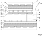
- FIG. 1 is a schematic sectional view of one embodiment of a chip stack comprising a main chip 2.
- the main chip 2 has a first face 4 and a second face 6.
- the main chip 2 comprises, on the side of the first face 4, electronic components to be protected 8 containing confidential data.
- the confidential data are by example banking data, personal data or encryption keys.
- the chip 2 further comprises an interconnection network 12 covering the components 8.
- the interconnection network 12 is made up of metallization levels, not shown, connected to each other, and to the components 8 of the chip, by conductive vias, not shown.
- the main chip 2 further comprises contact pads 14.
- the contact pads 14 are located at the periphery of the chip 2 and are capable of being connected by conductive wires 16 to external circuits, for example voltage sources, clock signal sources or input/output terminals.
- Auxiliary chips 18 and 20 may each contain electronic components 34. Components 34 do not contain confidential data and there is no need to protect them against hacker attacks. Each chip 18 or 20 then comprises an interconnection network 36 covering the components 34 and connecting them together.
- Each interconnection network 36 is covered with an insulating layer 38 containing at least one conductive track not shown in Figure 1 extending opposite the components to be protected. Each network 36 is separated from the conductive track by an insulating layer 39.
- the conductive tracks will be described in more detail in relation to the Figures 2 and 3 .
- each chip 18 and 20 is covered with a metal plane 40 connected to ground.
- Each metal plane 40 is separated from the associated layer 38 by an insulating layer 41.
- Each metal plane 40 extends at least over the area located opposite the components 8 to be protected.
- Each metal plane 40 extends, for example, over the entire chip 18 or 20.
- the metal planes 40 are for example made of copper or aluminum and have a thickness for example between 1 and 5 ⁇ m.
- the auxiliary chips 18 and 20 are located on each side of the main chip 2.
- the chips 18 and 20 are located in such a way that the metal plane 40 of the chip 18 is opposite the first face 4 of the chip 2 and the metal plane 40 of the chip 20 is opposite the second face 6 of the chip 2.
- the chip 18 is fixed to the chip 2 by metal elements 24 and the chip 20 is fixed to the chip 2 by metal elements 28.
- the metal elements 24 and 28 are, for example, metal balls connecting pads, not shown, of the chips 18 and 20 to pads of the chip 2.
- the height of the elements 24 and 28, corresponding to the distance between the chip 18 or the chip 20 and the chip 2, is, for example, between 10 and 50 ⁇ m.
- At least some of the elements 24 are connected to the interconnection network 12 of the chip 2. These elements 24 can be connected to the metal plane 40 of the chip 18, to the conductive track(s) formed in the layer 38 of the chip 18 by means of isolated vias (not shown) crossing the metal plane 40 of the chip 18, or to the interconnection network 36 of the chip 18 by means of isolated vias (not shown) crossing the metal plane 40 and the layer 38 of the chip 18.
- At least some of the elements 28 are connected to the interconnection network 12 of the chip 2 by means of vias 42 crossing the chip 2 from the second face 6 to the network 12. These elements 28 can be connected to the plane 40 of the chip 20, to the conductive track(s) of the layer 38 of the chip 20 by means of an isolated via (not shown) crossing the metal plane 40 of the chip 20, or to the interconnection network 36 of the chip 20 by means of isolated vias (not shown) crossing the metal plane 40 and the layer 38 of the chip 20.
- Chip 18, in the example of the Figure 1 has dimensions smaller than the dimensions of chip 2 so as to allow access to the contact pads 14.
- the dimensions of the chip 18 are nevertheless at least sufficient to cover all of the components to be protected 8 and the interconnection network 12 connecting them.
- Chip 20 in the example of the Figure 1 has dimensions substantially equal to those of chip 2.
- the dimensions of chip 20 may nevertheless be different from those of chip 2, while remaining sufficient to cover all of the components 8 to be protected.
- the connections made by the conductive wires 16 can be made in a different manner.
- the contact pads 14 can be located on the face of the chip 18 opposite the metal plane 40 and the connection with the chip 2 can then be made by means of metal elements 24 and vias passing through the chip 18 to the contact pads 14.
- the chip 18 can then have dimensions substantially equal to those of the chip 2.
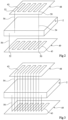
- FIG. 2 is a schematic and simplified perspective view of the embodiment described in relation to the Figure 1 representing an example of a conductive track pattern.
- Chip 18 is represented here only by a plane 48 containing a conductive track 43.
- chip 20 is represented only by a plane 49 containing a conductive track 43.
- Chip 2 is represented only by a parallelepiped.
- the conductive track 43 of each layer 38 has a serpentine shape and has ends 50 and 52.
- the ends 50 of the tracks are connected together by a connection 54.
- the connection 54 corresponds, for example, in relation to the Figure 1 , to an isolated via crossing the metal plane 40 of the chip 18, to a metal element 24, to the interconnection network 12, to a via 42 crossing the chip 2, to a metal element 28 and to another via crossing the metal plane 40 of the chip 20.
- the conductive tracks 43 and the connection 54 therefore form an electrically continuous path going from a end 52 to the other.
- the ends 52 of the conductive tracks 43 are connected, by connections 56, to a device, not shown, adapted to detect the interruption of the electrically continuous path, that is to say the total or partial interruption of one of the conductive tracks 43 or the interruption of one of the connections 54 or 56.
- the device is located among the components to be protected (8, Figure 1 ) of chip 2. Thus, the device is protected from hackers who cannot then interfere with its operation, for example by disabling it.
- the patterns of the conductive tracks are tight patterns, that is to say that the spacing between two neighboring portions of conductive track is relatively small.
- the choice of the dimensions of the tracks and the spacing separating neighboring portions of track is made according to existing etching technologies, in such a way that any attempt at etching attack results in the total or partial interruption of a conductive track.
- a step of detecting interruption of the conductive tracks 43 and of the connection 54 can for example be carried out after a manual command, automatically at regular intervals or at each start of the chip, during initialization.
- FIG. 3 is a schematic and simplified perspective view of an alternative embodiment.
- the figure represents another example of a conductive track pattern.
- the Figure 3 includes elements identical to elements of the Figure 2 , designated by the same references.
- the Figure 3 represents an electrically continuous path starting at chip 2, where it is connected to a device, not shown, for detecting interruption of the path. The path then alternates, via a connection 56 and connections 54 described previously, between conductive tracks 43 of chips 18 and 20 before joining chip 2 and the detection device via a connection 56.
- each electrically distinct continuous path each connected to a device adapted to detect the interruption of the path and located among the components to be protected 8 of the chip 2.
- a device adapted to detect the interruption of the path and located among the components to be protected 8 of the chip 2.
- Each of these paths makes it possible to detect the piercing of the chip, 18 or 20, in which it is formed, or its separation from the chip 2.
- Physical attacks such as drilling one of the chips 18 or 20, for example to place a contact at the interconnection network, can reach the components 34 and the interconnection networks 36 of said chip 18 or 20.
- the chips 18 and 20 do not contain confidential data.
- Such an attack targeting the chip 2, which contains confidential data, causes a total or partial interruption of a conductive track of a layer 38 and is detected. Removing one of the chips 18 and 20 so as to have access to the chip 2 causes the interruption of a connection 54 or 56 and the detection of the attack.
- the auxiliary chips 18 and 20 may also include laser beam detectors, for example photodiodes, so as to detect a laser beam attack.
- the auxiliary chips 18 and 20 may also include additional protection devices.
- the metal planes 40 connected to ground form a Faraday cage around the components 8. It is therefore not possible for a hacker to analyze the electromagnetic emissions of chip 2.
- An advantage of the embodiments described above is that the chip 2 that is to be protected is not modified by the protection devices.
- the metal planes 40 and the conductive tracks 43, as well as the insulating layers separating them may not be located, as in the Figure 1 , in chips 18 and 20 different from the protected chip 2, but can cover the first and second faces of the chip 2, framing the components 8.
- the conductive tracks 43 of the layers 38 may, for example, take the form of one or more spirals or the form of lines.
- the patterns of the conductive tracks 43 of a chip 18 or 20 may extend over several levels.
Landscapes
- Engineering & Computer Science (AREA)
- Physics & Mathematics (AREA)
- General Physics & Mathematics (AREA)
- Computer Hardware Design (AREA)
- Computer Security & Cryptography (AREA)
- General Engineering & Computer Science (AREA)
- Microelectronics & Electronic Packaging (AREA)
- Theoretical Computer Science (AREA)
- Semiconductor Integrated Circuits (AREA)
- Geometry (AREA)
- Storage Device Security (AREA)
Description
- La présente demande concerne le domaine des puces électroniques et vise plus particulièrement un empilement de puces comprenant une puce protégée contre des attaques de pirates.
- Certaines puces électroniques telles que des puces de cartes bancaires peuvent contenir des données confidentielles susceptibles d'être convoitées par des pirates. Ces données confidentielles peuvent être contenues dans des circuits situés du côté de la face avant de la puce. Pour obtenir ces données, un pirate peut mener une attaque à partir de la face arrière ou de la face avant de la puce.
- Dans un type d'attaque, dit attaque par gravure, le pirate grave une partie de la face arrière de la puce. A partir de cette partie gravée, le pirate grave des cavités de quelques micromètres de largeur, par exemple en utilisant un faisceau d'ions, qui s'étendent vers la face avant jusqu'au niveau des circuits. Des contacts électriques avec des éléments des circuits sont ensuite créés dans ces cavités, et le pirate utilise ces contacts pour analyser la puce en fonctionnement.
- Dans un autre type d'attaque, le pirate balaye la puce par des impulsions laser. L'impact du faisceau laser perturbe le fonctionnement de la puce. C'est l'observation des conséquences de ces perturbations sur l'activité des circuits qui permet au pirate de mener à bien son attaque. Pour perturber le fonctionnement de la puce, le pirate peut aussi appliquer des potentiels positifs ou négatifs au moyen d'une sonde en contact avec la puce, ou induire des courants ou des tensions dans des éléments des circuits au moyen d'une bobine disposée à proximité de la puce. Ce type d'attaque est appelé attaque par injection de faute.
- Dans un autre type d'attaque, le pirate utilise le rayonnement électromagnétique émis par la puce de manière à obtenir les données confidentielles. En effet, les commutations des portes logiques constituant un circuit produisent des émissions électromagnétiques. Or, dans un circuit, toutes les portes logiques ne commutent pas à chaque cycle d'horloge et donc les émissions électromagnétiques seront proportionnelles au nombre de portes logiques commutant. Grâce à l'utilisation de certains algorithmes d'analyse mathématique (distance de Hamming...), il est possible de retrouver la clé de chiffrement de la puce en se basant sur une analyse des variations des émissions électromagnétiques du circuit.
- Les détecteurs d'attaques connus présentent tous un ou plusieurs des inconvénients suivants. Certains ne permettent de détecter qu'un nombre limité de type d'attaques, souvent un seul. Certains sont visibles pour le pirate. L'ajout de certains détecteurs entraine des modifications dans le procédé de fabrication. Des détecteurs d'attaques sont connus des documents
WO 2015/000813 A1 etDE 199 40 759 A1 . - Plus particulièrement, le premier document montre un empilement de puces comprenant:
- une puce principale contenant des composants à protéger; et
- une puce auxiliaire en regard d'une face de la puce principale, une zone de la puce auxiliaire en regard des composants à protéger comprenant au moins une piste conductrice isolée formant un motif serré en regard des composants à protéger, les extrémités de ladite au moins une piste conductrice étant accessibles au niveau de la puce principale.
- Le deuxième document montre un empilement de puces comprenant :
- une puce principale contenant des composants à protéger ; et
- une puce auxiliaire en regard de chaque face de la puce principale, une zone de chaque puce auxiliaire en regard des composants à protéger comprenant un plan métallique.
- Un mode de réalisation pallie tout ou partie des inconvénients des puces électroniques usuelles protégées contre des attaques.
- Ainsi, un mode de réalisation prévoit un empilement de puces selon la revendication comprenant : une puce principale contenant des composants à protéger ; et une puce auxiliaire en regard de chaque face de la puce principale, la zone de chaque puce auxiliaire en regard des composants à protéger comprenant un plan métallique connecté à la masse, et au moins une piste conductrice isolée formant un motif serré en regard des composants à protéger, les extrémités de ladite au moins une piste conductrice étant accessibles au niveau de la puce principale, le plan métallique de chaque puce auxiliaire étant situé entre la puce principale et la piste conductrice de ladite puce auxiliaire.
- Selon un mode de réalisation, le motif formé par les pistes conductrices est un serpentin.
- Selon un mode de réalisation, le motif formé par les pistes conductrices est une spirale.
- Selon un mode de réalisation, une extrémité d'une piste conductrice d'une puce auxiliaire est connectée à une extrémité d'une piste conductrice de l'autre puce auxiliaire.
- Selon un mode de réalisation, le dispositif est adapté à détecter une interruption de la connexion entre les pistes conductrices.
- Selon un mode de réalisation, les pistes conductrices sont connectées à un dispositif adapté à détecter des interruptions des pistes conductrices.
- Selon un mode de réalisation, les puces auxiliaires sont fixées à la puce principale par des billes métalliques.
- Selon un mode de réalisation, les puces auxiliaires comprennent des composants électroniques.
- Selon un mode de réalisation, le plan métallique de chaque puce auxiliaire s'étend sur toute la surface de la puce auxiliaire correspondante.
- Selon un mode de réalisation, les dimensions d'une des puces auxiliaires sont inférieures à celles de l'autre puce auxiliaire.
- Un mode de réalisation prévoit un procédé de protection de composants d'une puce principale contenant des composants à protéger, le procédé selon la revendication indépendante 11 comprenant les étapes suivantes : prévoir des puces auxiliaires comprenant chacune un plan métallique connecté à la masse, et au moins une piste conductrice isolée formant un motif serré ; monter les puces auxiliaires de part et d'autre de la puce principale de telle manière que les plans métalliques et les pistes conductrices soient en regard des composants à protéger, le plan métallique de chaque puce auxiliaire étant situé entre la puce principale et la piste conductrice de ladite puce auxiliaire ; connecter les extrémités des pistes conductrices avec la puce principale.
- Ces caractéristiques et avantages, ainsi que d'autres, seront exposés en détail dans la description suivante de modes de réalisation particuliers faite à titre non limitatif en relation avec les figures jointes parmi lesquelles :
- la
figure 1 est une vue en coupe, schématique, d'un mode de réalisation d'un empilement de puces comprenant une puce protégée ; et - les
figures 2 et 3 sont des vues en perspective, schématiques et simplifiées, d'exemples de mise en oeuvre de pistes conductrices. - De mêmes éléments ont été désignés par de mêmes références dans les différentes figures et, de plus, les diverses figures ne sont pas tracées à l'échelle. Par souci de clarté, seuls les éléments utiles à la compréhension des modes de réalisation décrits ont été représentés et sont détaillés. En particulier, les composants des différentes puces ne sont pas décrits en détail.
- Sauf précision contraire, le terme "sensiblement" signifie à 10 % près, de préférence à 5 % près.
- L'expression "interruption d'une piste conductrice" doit être comprise comme signifiant soit une interruption totale de la piste soit une interruption partielle, résultant en modification de la résistance de la piste.
- La
figure 1 est une vue en coupe schématique d'un mode de réalisation d'un empilement de puces comprenant une puce principale 2. La puce principale 2 a une première face 4 et une seconde face 6. - La puce principale 2 comporte, du côté de la première face 4, des composants électroniques à protéger 8 contenant des données confidentielles. Les données confidentielles sont par exemple des données bancaires, des données personnelles ou des clés de cryptage.
- La puce 2 comprend, de plus, un réseau d'interconnexion 12 recouvrant les composants 8. Le réseau d'interconnexion 12 est constitué de niveaux de métallisation, non représentés, connectés entre eux, et aux composants 8 de la puce, par des vias conducteurs, non représentés.
- La puce principale 2 comprend en outre des plots de contact 14. Dans la
figure 1 , les plots de contact 14 sont situés à la périphérie de la puce 2 et sont susceptibles d'être connectés par des fils conducteurs 16 à des circuits extérieurs, par exemple des sources de tension, des sources de signaux d'horloge ou des bornes entrées/sorties. - Des puces auxiliaires 18 et 20 peuvent contenir chacune des composants électroniques 34. Les composants 34 ne contiennent pas de données confidentielles et il n'est pas nécessaire de les protéger contre des attaques de pirates. Chaque puce 18 ou 20 comprend alors un réseau d'interconnexion 36 recouvrant les composants 34 et les connectant entre eux.
- Chaque réseau d'interconnexion 36 est recouvert d'une couche isolante 38 contenant au moins une piste conductrice non représentée en
figure 1 s'étendant en regard des composants à protéger. Chaque réseau 36 est séparé de la piste conductrice par une couche isolante 39. Les pistes conductrices seront décrites plus en détail en relation avec lesfigures 2 et 3 . - La couche 38 de chaque puce 18 et 20 est recouverte, d'un plan métallique 40 connecté à la masse. Chaque plan métallique 40 est séparé de la couche 38 associée par une couche isolante 41. Chaque plan métallique 40 s'étend au moins sur la zone située en regard des composants 8 à protéger. Chaque plan métallique 40 s'étend, par exemple, sur toute la puce 18 ou 20.
- Les plans métalliques 40 sont par exemple en cuivre ou en aluminium et ont une épaisseur par exemple comprise entre 1 et 5 µm.
- Les puces auxiliaires 18 et 20 sont situées de chaque côté de la puce principale 2. Les puces 18 et 20 sont situées de telle manière que le plan métallique 40 de la puce 18 est en regard de la première face 4 de la puce 2 et que le plan métallique 40 de la puce 20 est en regard de la seconde face 6 de la puce 2. La puce 18 est fixée à la puce 2 par des éléments métalliques 24 et la puce 20 est fixée à la puce 2 par des éléments métalliques 28.
- Les éléments métalliques 24 et 28 sont par exemple des billes métalliques reliant des plots, non représentés, des puces 18 et 20 à des plots de la puce 2. La hauteur des éléments 24 et 28, correspondant à la distance entre la puce 18 ou la puce 20 et la puce 2, est par exemple comprise entre 10 et 50 µm.
- Au moins certains des éléments 24 sont connectés au réseau d'interconnexion 12 de la puce 2. Ces éléments 24 peuvent être connectés au plan métallique 40 de la puce 18, à la ou aux pistes conductrices formées dans la couche 38 de la puce 18 par l'intermédiaire de vias isolés non représentés traversant le plan métallique 40 de la puce 18, ou au réseau d'interconnexion 36 de la puce 18 par l'intermédiaire de vias isolés non représentés traversant le plan métallique 40 et la couche 38 de la puce 18.
- Au moins certains des éléments 28 sont connectés au réseau d'interconnexion 12 de la puce 2 par l'intermédiaire de vias 42 traversant la puce 2 depuis la seconde face 6 jusqu'au réseau 12. Ces éléments 28 peuvent être connectés au plan 40 de la puce 20, à la ou aux pistes conductrices de la couche 38 de la puce 20 par l'intermédiaire d'un via isolé non représenté traversant le plan métallique 40 de la puce 20, ou au réseau d'interconnexion 36 de la puce 20 par l'intermédiaire de vias isolés non représentés traversant le plan métallique 40 et la couche 38 de la puce 20.
- Par souci de clarté, un seul via 42 a été représenté en
figure 1 . Cependant, il peut y en avoir autant que nécessaire. - La puce 18, dans l'exemple de la
figure 1 , a des dimensions inférieures aux dimensions de la puce 2 de manière à permettre l'accès aux plots de contact 14. Les dimensions de la puce 18 sont néanmoins au moins suffisantes pour recouvrir l'ensemble des composants à protéger 8 et le réseau d'interconnexion 12 les connectant. - La puce 20, dans l'exemple de la
figure 1 , a des dimensions sensiblement égales à celles de la puce 2. Les dimensions de la puce 20 peuvent néanmoins être différentes de celles de la puce 2, tout en restant suffisantes pour recouvrir l'ensemble des composants 8 à protéger. - A titre de variante, non représentée, il est possible pour les connexions faites par les fils conducteurs 16 d'être effectués de manière différente. Par exemple, les plots de contact 14 peuvent être situés sur la face de la puce 18 opposée au plan métallique 40 et la connexion avec la puce 2 peut alors être faite par l'intermédiaire d'éléments métalliques 24 et de vias traversant la puce 18 jusqu'aux plots de contact 14. La puce 18 peut alors avoir des dimensions sensiblement égales à celles de la puce 2.
- La
figure 2 est une vue en perspective, schématique et simplifiée, du mode de réalisation décrit en relation avec lafigure 1 représentant un exemple de motif de piste conductrice. La puce 18 n'est représentée ici que par un plan 48 contenant une piste conductrice 43. De même, la puce 20 n'est représentée que par un plan 49 contenant une piste conductrice 43. La puce 2 est uniquement représentée par un parallélépipède. - Dans cet exemple, la piste conductrice 43 de chaque couche 38 a une forme de serpentin et a des extrémités 50 et 52. Les extrémités 50 des pistes sont connectées ensemble par une connexion 54. La connexion 54 correspond par exemple, en relation avec la
figure 1 , à un via isolé traversant le plan métallique 40 de la puce 18, à un élément métallique 24, au réseau d'interconnexion 12, à un via 42 traversant la puce 2, à un élément métallique 28 et à un autre via traversant le plan métallique 40 de la puce 20. Les pistes conductrices 43 et la connexion 54 forment donc un chemin continu électriquement allant d'une extrémité 52 à l'autre. Les extrémités 52 des pistes conductrices 43 sont connectées, par des connexions 56, à un dispositif, non représenté, adapté à détecter l'interruption du chemin continu électriquement, c'est-à-dire l'interruption totale ou partielle d'une des pistes conductrices 43 ou l'interruption d'une des connexions 54 ou 56. Le dispositif est situé parmi les composants à protéger (8,figure 1 ) de la puce 2. Ainsi, le dispositif est protégé des pirates qui ne peuvent alors pas interférer avec son fonctionnement, par exemple en le désactivant. - Les motifs des pistes conductrices sont des motifs serrés, c'est-à-dire que l'espacement entre deux portions voisines de piste conductrice est relativement faible. Le choix des dimensions des pistes et de l'espacement séparant des portions voisines de piste est fait en fonction des technologies de gravure existantes, de telle manière que toute tentative d'attaque par gravure entraine l'interruption totale ou partielle d'une piste conductrice.
- Une étape de détection d'interruption des pistes conductrices 43 et de la connexion 54 peut par exemple être effectuée après une commande manuelle, de manière automatique à intervalles réguliers ou à chaque démarrage de la puce, lors de l'initialisation.
- La
figure 3 est une vue en perspective, schématique et simplifiée, d'une variante de réalisation. La figure représente un autre exemple de motif de piste conductrice. Lafigure 3 comprend des éléments identiques à des éléments de lafigure 2 , désignés par de mêmes références. Lafigure 3 représente un chemin électriquement continu débutant par la puce 2, où il est connecté à un dispositif, non représenté, de détection d'interruption du chemin. Le chemin alterne ensuite, par l'intermédiaire d'une connexion 56 et de connexions 54 décrites précédemment, entre des pistes conductrices 43 des puces 18 et 20 avant de rejoindre la puce 2 et le dispositif de détection par une connexion 56. - A titre de variante, il est possible de former plusieurs chemins continus électriquement distincts, chacun connecté à un dispositif adapté à détecter l'interruption du chemin et situé parmi les composants à protéger 8 de la puce 2. Par exemple, il est possible de former un chemin allant de la puce 2 à la couche 38 de la puce 18, s'étendant dans cette couche 38 et rejoignant la puce 2, ainsi qu'un chemin similaire pour la puce 20. Chacun de ces chemins permet de détecter le perçage de la puce, 18 ou 20, dans laquelle il est formé, ou sa séparation de la puce 2. Il n'y a alors pas de connexion directe (par exemple une connexion 54) entre les pistes de la puce 18 et de la puce 20.
- Les attaques physiques telles que le perçage d'une des puces 18 ou 20, par exemple pour placer un contact au niveau du réseau d'interconnexion, peuvent atteindre les composants 34 et les réseaux d'interconnexion 36 de ladite puce 18 ou 20. Cependant les puces 18 et 20 ne contiennent pas de données confidentielles. Une telle attaque visant la puce 2, qui contient des données confidentielles, provoque une interruption totale ou partielle d'une piste conductrice d'une couche 38 et est détectée. Le retrait d'une des puces 18 et 20 de manière à avoir accès à la puce 2 provoque l'interruption d'une connexion 54 ou 56 et la détection de l'attaque.
- Les attaques laser peuvent, comme les attaques physiques, atteindre les puces 18 et 20. Cependant, les plans métalliques 40 arrêtent le faisceau laser qui ne peut donc atteindre la puce 2. Les puces auxiliaires 18 et 20 peuvent aussi comprendre des détecteurs de faisceau laser, par exemple des photodiodes, de manière à repérer une attaque par faisceau laser. Les puces auxiliaires 18 et 20 peuvent aussi comprendre des dispositifs de protection supplémentaires.
- Les plans métalliques 40 connectés à la masse, forment une cage de Faraday autour des composants 8. Il n'est donc pas possible pour un pirate d'analyser les émissions électromagnétiques de la puce 2.
- Un avantage des modes de réalisation décrits précédemment est que la puce 2 que l'on cherche à protéger n'est pas modifiée par les dispositifs de protection.
- A titre de variante qui ne fait pas partie de l'invention revendiquée, les plans métalliques 40 et les pistes conductrices 43, ainsi que les couches isolantes les séparant, peuvent ne pas être situées, comme dans la
figure 1 , dans des puces 18 et 20 différentes de la puce protégée 2, mais peuvent recouvrir les première et seconde faces de la puce 2, encadrant les composants 8. - Un avantage de ces modes de réalisation est que le détecteur d'interruption des pistes conductrices est parmi les composants 8 et est protégé. Il ne peut donc être atteint par le pirate.
- Des modes de réalisation particuliers ont été décrits. Diverses variantes et modifications apparaîtront à l'homme de l'art. En particulier, d'autres motifs sont possibles pour les pistes conductrices 43 des couches 38. Les pistes conductrices 43 peuvent par exemple prendre la forme d'une ou plusieurs spirales ou la forme de lignes. Les motifs des pistes conductrices 43 d'une puce 18 ou 20 peuvent s'étendre sur plusieurs niveaux.
Claims (11)
- Empilement de puces comprenant :une puce principale (2) contenant des composants à protéger (8) ; etune puce auxiliaire (18, 20) en regard de chaque face (4, 6) de la puce principale (2), une zone de chaque puce auxiliaire en regard des composants à protéger (8) comprenant un plan métallique (40) connecté à la masse, et au moins une piste conductrice isolée (43) formant un motif serré en regard des composants à protéger (8), les extrémités (50, 52) de ladite au moins une piste conductrice étant accessibles au niveau de la puce principale (2), le plan métallique de chaque puce auxiliaire étant situé entre la puce principale et la piste conductrice de ladite puce auxiliaire.
- Empilement de puces selon la revendication 1, dans lequel le motif formé par les pistes conductrices (43) est un serpentin.
- Empilement de puces selon la revendication 1, dans lequel le motif formé par les pistes conductrices (43) est une spirale.
- Empilement de puces selon l'une quelconque des revendications 1 à 3, dans lequel une extrémité (50) d'une piste conductrice (43) d'une puce auxiliaire (18, 20) est connectée à une extrémité (50) d'une piste conductrice (43) de l'autre puce auxiliaire (18, 20).
- Empilement de puces selon la revendication 4, dans lequel les pistes conductrices (43) sont connectées à un dispositif adapté à détecter des interruptions des pistes conductrices (43).
- Empilement de puces selon l'une quelconque des revendications 1 à 5, dans lequel le dispositif est adapté à détecter une interruption de la connexion (54, 56) entre les pistes conductrices (43).
- Empilement de puces selon l'une quelconque des revendications 1 à 6, dans lequel les puces auxiliaires (18, 20) sont fixées à la puce principale (2) par des billes métalliques (24, 28).
- Empilement de puces selon l'une quelconque des revendications 1 à 7, dans lequel les puces auxiliaires (18, 20) comprennent des composants électroniques (34).
- Empilement de puces selon l'une quelconque des revendications 1 à 8, dans lequel le plan métallique (40) de chaque puce auxiliaire (18, 20) s'étend sur toute la surface de la puce auxiliaire correspondante.
- Empilement de puces selon l'une quelconque des revendications 1 à 9, dans lequel les dimensions d'une des puces auxiliaires (18, 20) sont inférieures à celles de la puce principale(2).
- Procédé de protection de composants (8) d'une puce principale (2) contenant des composants à protéger, le procédé comprenant les étapes suivantes :prévoir des puces auxiliaires (18, 20) comprenant chacune un plan métallique (40) connecté à la masse, et au moins une piste conductrice isolée (43) formant un motif serré ;monter les puces auxiliaires (18, 20) de part et d'autre de la puce principale (2) de telle manière que les plans métalliques (40) et les pistes conductrices (43) soient en regard des composants à protéger (8), le plan métallique de chaque puce auxiliaire étant situé entre la puce principale et la piste conductrice de ladite puce auxiliaire ; etconnecter les extrémités (50, 52) des pistes conductrices (43) avec la puce principale (2).
Applications Claiming Priority (1)
| Application Number | Priority Date | Filing Date | Title |
|---|---|---|---|
| FR1758340A FR3071101A1 (fr) | 2017-09-11 | 2017-09-11 | Empilement de puces |
Publications (2)
| Publication Number | Publication Date |
|---|---|
| EP3454368A1 EP3454368A1 (fr) | 2019-03-13 |
| EP3454368B1 true EP3454368B1 (fr) | 2025-05-28 |
Family
ID=61599238
Family Applications (1)
| Application Number | Title | Priority Date | Filing Date |
|---|---|---|---|
| EP18192582.7A Active EP3454368B1 (fr) | 2017-09-11 | 2018-09-04 | Empilement de puces protegé contre le piratage de données |
Country Status (4)
| Country | Link |
|---|---|
| US (1) | US10473709B2 (fr) |
| EP (1) | EP3454368B1 (fr) |
| CN (2) | CN109494207B (fr) |
| FR (1) | FR3071101A1 (fr) |
Families Citing this family (1)
| Publication number | Priority date | Publication date | Assignee | Title |
|---|---|---|---|---|
| FR3071101A1 (fr) * | 2017-09-11 | 2019-03-15 | Stmicroelectronics (Rousset) Sas | Empilement de puces |
Citations (1)
| Publication number | Priority date | Publication date | Assignee | Title |
|---|---|---|---|---|
| DE19940759A1 (de) * | 1999-08-27 | 2001-03-22 | Infineon Technologies Ag | Schaltungsanordnung und Verfahren zu deren Herstellung |
Family Cites Families (12)
| Publication number | Priority date | Publication date | Assignee | Title |
|---|---|---|---|---|
| JP2002543621A (ja) * | 1999-05-03 | 2002-12-17 | インフィネオン テクノロジース アクチエンゲゼルシャフト | 多次元に積層されたチップステープルを保安するための方法および装置 |
| US7065656B2 (en) * | 2001-07-03 | 2006-06-20 | Hewlett-Packard Development Company, L.P. | Tamper-evident/tamper-resistant electronic components |
| US7498644B2 (en) * | 2002-06-04 | 2009-03-03 | Nds Limited | Prevention of tampering in electronic devices |
| TW529772U (en) * | 2002-06-06 | 2003-04-21 | Protectronics Technology Corp | Surface mountable laminated circuit protection device |
| JP2006228910A (ja) * | 2005-02-16 | 2006-08-31 | Matsushita Electric Ind Co Ltd | 半導体装置 |
| WO2009035688A1 (fr) * | 2007-09-13 | 2009-03-19 | Broadcom Corporation | Protection à grille maillée |
| US8455990B2 (en) * | 2009-02-25 | 2013-06-04 | Conexant Systems, Inc. | Systems and methods of tamper proof packaging of a semiconductor device |
| FR2998419B1 (fr) * | 2012-11-21 | 2015-01-16 | St Microelectronics Rousset | Protection d'un circuit integre contre des attaques |
| GB201311834D0 (en) * | 2013-07-02 | 2013-08-14 | Qinetiq Ltd | Electronic hardware assembly |
| FR3011978A1 (fr) * | 2013-10-15 | 2015-04-17 | St Microelectronics Grenoble 2 | Systeme electronique comprenant des dispositifs electroniques empiles comprenant des puces de circuits integres |
| EP3188231B1 (fr) * | 2015-12-29 | 2023-01-04 | Secure-IC SAS | Système et procédé pour protéger un dispositif de circuit intégré |
| FR3071101A1 (fr) * | 2017-09-11 | 2019-03-15 | Stmicroelectronics (Rousset) Sas | Empilement de puces |
-
2017
- 2017-09-11 FR FR1758340A patent/FR3071101A1/fr not_active Withdrawn
-
2018
- 2018-09-04 EP EP18192582.7A patent/EP3454368B1/fr active Active
- 2018-09-06 CN CN201811038819.1A patent/CN109494207B/zh active Active
- 2018-09-06 CN CN201821457978.0U patent/CN208596672U/zh not_active Withdrawn - After Issue
- 2018-09-07 US US16/125,096 patent/US10473709B2/en active Active
Patent Citations (1)
| Publication number | Priority date | Publication date | Assignee | Title |
|---|---|---|---|---|
| DE19940759A1 (de) * | 1999-08-27 | 2001-03-22 | Infineon Technologies Ag | Schaltungsanordnung und Verfahren zu deren Herstellung |
Also Published As
| Publication number | Publication date |
|---|---|
| CN208596672U (zh) | 2019-03-12 |
| US10473709B2 (en) | 2019-11-12 |
| US20190079133A1 (en) | 2019-03-14 |
| FR3071101A1 (fr) | 2019-03-15 |
| CN109494207B (zh) | 2022-11-08 |
| CN109494207A (zh) | 2019-03-19 |
| EP3454368A1 (fr) | 2019-03-13 |
Similar Documents
| Publication | Publication Date | Title |
|---|---|---|
| EP1700256B1 (fr) | Protection d'une puce de circuit intégré contenant des données confidentielles | |
| EP2535932B1 (fr) | Puce de circuit intégré comprenant un dispositif de protection contre des attaques | |
| EP2866259B1 (fr) | Puce électronique comprenant des moyens de protection de sa face arrière | |
| TW202312358A (zh) | 用於接合結構的保護性半導體元件 | |
| EP3291293B1 (fr) | Puce protégée contre les attaques face arrière | |
| EP2535933B1 (fr) | Puce de circuit intégré comprenant un dispositif de protection contre des attaques | |
| EP3086368A2 (fr) | Puce electronique comportant une face arriere protegee | |
| FR2971366A1 (fr) | Micro plaquette de semi-conducteur comprenant des moyens de protection contre une attaque physique | |
| WO2010058094A1 (fr) | Dispositif de protection d'un boitier de circuit intégré électronique contre les intrusions par voie physique ou chimique | |
| KR20150077354A (ko) | 커버 기판 상의 반도체 디바이스 및 그 제조 방법 | |
| EP3454368B1 (fr) | Empilement de puces protegé contre le piratage de données | |
| EP3151277B1 (fr) | Circuit intégré sécurisé | |
| EP3371735B1 (fr) | Corps de lecteur de carte à mémoire à treillis de protection recto-verso | |
| EP3316295B1 (fr) | Dispositif comprenant un empilement de puces électroniques | |
| EP1183642B1 (fr) | Dispositif a circuit integre securise contre des attaques procedant par destruction controlee d'une couche complementaire | |
| EP3525236B1 (fr) | Procédé de détection d'une atteinte à l'intégrité d'un substrat semi-conducteur d'un circuit intégré depuis sa face arrière, et dispositif correspondant | |
| EP3435411B1 (fr) | Puce électronique protégée contre des attaques pirates depuis la face arrière | |
| Zhu et al. | A novel silicon interposer based high security integration approach for microsystem | |
| FR2863746A1 (fr) | Circuit integre protege par bouclier actif | |
| EP3593380A1 (fr) | Puce electronique | |
| FR2910708A1 (fr) | Protection de donnees confidentielles dans les circuits integres | |
| FR3062952A1 (fr) | Condensateur de decouplage | |
| FR3057088A1 (fr) | Detecteur laser picosecondes | |
| FR3164058A1 (fr) | Dispositif comprenant une piste métallique et procédé de fabrication du dispositif | |
| EP3985719A1 (fr) | Boitier-systeme electronique comprenant des faces laterales protegees |
Legal Events
| Date | Code | Title | Description |
|---|---|---|---|
| PUAI | Public reference made under article 153(3) epc to a published international application that has entered the european phase |
Free format text: ORIGINAL CODE: 0009012 |
|
| STAA | Information on the status of an ep patent application or granted ep patent |
Free format text: STATUS: REQUEST FOR EXAMINATION WAS MADE |
|
| 17P | Request for examination filed |
Effective date: 20180904 |
|
| AK | Designated contracting states |
Kind code of ref document: A1 Designated state(s): AL AT BE BG CH CY CZ DE DK EE ES FI FR GB GR HR HU IE IS IT LI LT LU LV MC MK MT NL NO PL PT RO RS SE SI SK SM TR |
|
| AX | Request for extension of the european patent |
Extension state: BA ME |
|
| STAA | Information on the status of an ep patent application or granted ep patent |
Free format text: STATUS: EXAMINATION IS IN PROGRESS |
|
| 17Q | First examination report despatched |
Effective date: 20210430 |
|
| GRAP | Despatch of communication of intention to grant a patent |
Free format text: ORIGINAL CODE: EPIDOSNIGR1 |
|
| STAA | Information on the status of an ep patent application or granted ep patent |
Free format text: STATUS: GRANT OF PATENT IS INTENDED |
|
| RIC1 | Information provided on ipc code assigned before grant |
Ipc: G06K 19/073 20060101ALI20250115BHEP Ipc: H01L 25/065 20060101ALI20250115BHEP Ipc: H01L 23/58 20060101AFI20250115BHEP |
|
| INTG | Intention to grant announced |
Effective date: 20250124 |
|
| GRAS | Grant fee paid |
Free format text: ORIGINAL CODE: EPIDOSNIGR3 |
|
| GRAA | (expected) grant |
Free format text: ORIGINAL CODE: 0009210 |
|
| STAA | Information on the status of an ep patent application or granted ep patent |
Free format text: STATUS: THE PATENT HAS BEEN GRANTED |
|
| AK | Designated contracting states |
Kind code of ref document: B1 Designated state(s): AL AT BE BG CH CY CZ DE DK EE ES FI FR GB GR HR HU IE IS IT LI LT LU LV MC MK MT NL NO PL PT RO RS SE SI SK SM TR |
|
| REG | Reference to a national code |
Ref country code: GB Ref legal event code: FG4D Free format text: NOT ENGLISH |
|
| REG | Reference to a national code |
Ref country code: CH Ref legal event code: EP |
|
| REG | Reference to a national code |
Ref country code: DE Ref legal event code: R096 Ref document number: 602018082253 Country of ref document: DE |
|
| REG | Reference to a national code |
Ref country code: IE Ref legal event code: FG4D Free format text: LANGUAGE OF EP DOCUMENT: FRENCH |
|
| REG | Reference to a national code |
Ref country code: NL Ref legal event code: MP Effective date: 20250528 |
|
| PG25 | Lapsed in a contracting state [announced via postgrant information from national office to epo] |
Ref country code: FI Free format text: LAPSE BECAUSE OF FAILURE TO SUBMIT A TRANSLATION OF THE DESCRIPTION OR TO PAY THE FEE WITHIN THE PRESCRIBED TIME-LIMIT Effective date: 20250528 Ref country code: ES Free format text: LAPSE BECAUSE OF FAILURE TO SUBMIT A TRANSLATION OF THE DESCRIPTION OR TO PAY THE FEE WITHIN THE PRESCRIBED TIME-LIMIT Effective date: 20250528 |
|
| PGFP | Annual fee paid to national office [announced via postgrant information from national office to epo] |
Ref country code: DE Payment date: 20250820 Year of fee payment: 8 |
|
| REG | Reference to a national code |
Ref country code: LT Ref legal event code: MG9D |
|
| PG25 | Lapsed in a contracting state [announced via postgrant information from national office to epo] |
Ref country code: NO Free format text: LAPSE BECAUSE OF FAILURE TO SUBMIT A TRANSLATION OF THE DESCRIPTION OR TO PAY THE FEE WITHIN THE PRESCRIBED TIME-LIMIT Effective date: 20250828 Ref country code: GR Free format text: LAPSE BECAUSE OF FAILURE TO SUBMIT A TRANSLATION OF THE DESCRIPTION OR TO PAY THE FEE WITHIN THE PRESCRIBED TIME-LIMIT Effective date: 20250829 |
|
| PG25 | Lapsed in a contracting state [announced via postgrant information from national office to epo] |
Ref country code: PL Free format text: LAPSE BECAUSE OF FAILURE TO SUBMIT A TRANSLATION OF THE DESCRIPTION OR TO PAY THE FEE WITHIN THE PRESCRIBED TIME-LIMIT Effective date: 20250528 Ref country code: NL Free format text: LAPSE BECAUSE OF FAILURE TO SUBMIT A TRANSLATION OF THE DESCRIPTION OR TO PAY THE FEE WITHIN THE PRESCRIBED TIME-LIMIT Effective date: 20250528 |
|
| PG25 | Lapsed in a contracting state [announced via postgrant information from national office to epo] |
Ref country code: BG Free format text: LAPSE BECAUSE OF FAILURE TO SUBMIT A TRANSLATION OF THE DESCRIPTION OR TO PAY THE FEE WITHIN THE PRESCRIBED TIME-LIMIT Effective date: 20250528 |
|
| PG25 | Lapsed in a contracting state [announced via postgrant information from national office to epo] |
Ref country code: HR Free format text: LAPSE BECAUSE OF FAILURE TO SUBMIT A TRANSLATION OF THE DESCRIPTION OR TO PAY THE FEE WITHIN THE PRESCRIBED TIME-LIMIT Effective date: 20250528 |
|
| PG25 | Lapsed in a contracting state [announced via postgrant information from national office to epo] |
Ref country code: RS Free format text: LAPSE BECAUSE OF FAILURE TO SUBMIT A TRANSLATION OF THE DESCRIPTION OR TO PAY THE FEE WITHIN THE PRESCRIBED TIME-LIMIT Effective date: 20250828 |
|
| PG25 | Lapsed in a contracting state [announced via postgrant information from national office to epo] |
Ref country code: IS Free format text: LAPSE BECAUSE OF FAILURE TO SUBMIT A TRANSLATION OF THE DESCRIPTION OR TO PAY THE FEE WITHIN THE PRESCRIBED TIME-LIMIT Effective date: 20250928 |
|
| PG25 | Lapsed in a contracting state [announced via postgrant information from national office to epo] |
Ref country code: LV Free format text: LAPSE BECAUSE OF FAILURE TO SUBMIT A TRANSLATION OF THE DESCRIPTION OR TO PAY THE FEE WITHIN THE PRESCRIBED TIME-LIMIT Effective date: 20250528 |
|
| REG | Reference to a national code |
Ref country code: DE Ref legal event code: R079 Ref document number: 602018082253 Country of ref document: DE Free format text: PREVIOUS MAIN CLASS: H01L0023580000 Ipc: H10W0029000000 |
|
| REG | Reference to a national code |
Ref country code: AT Ref legal event code: MK05 Ref document number: 1799148 Country of ref document: AT Kind code of ref document: T Effective date: 20250528 |
|
| PG25 | Lapsed in a contracting state [announced via postgrant information from national office to epo] |
Ref country code: DK Free format text: LAPSE BECAUSE OF FAILURE TO SUBMIT A TRANSLATION OF THE DESCRIPTION OR TO PAY THE FEE WITHIN THE PRESCRIBED TIME-LIMIT Effective date: 20250528 Ref country code: AT Free format text: LAPSE BECAUSE OF FAILURE TO SUBMIT A TRANSLATION OF THE DESCRIPTION OR TO PAY THE FEE WITHIN THE PRESCRIBED TIME-LIMIT Effective date: 20250528 Ref country code: SM Free format text: LAPSE BECAUSE OF FAILURE TO SUBMIT A TRANSLATION OF THE DESCRIPTION OR TO PAY THE FEE WITHIN THE PRESCRIBED TIME-LIMIT Effective date: 20250528 |
|
| PG25 | Lapsed in a contracting state [announced via postgrant information from national office to epo] |
Ref country code: CZ Free format text: LAPSE BECAUSE OF FAILURE TO SUBMIT A TRANSLATION OF THE DESCRIPTION OR TO PAY THE FEE WITHIN THE PRESCRIBED TIME-LIMIT Effective date: 20250528 |
|
| PG25 | Lapsed in a contracting state [announced via postgrant information from national office to epo] |
Ref country code: EE Free format text: LAPSE BECAUSE OF FAILURE TO SUBMIT A TRANSLATION OF THE DESCRIPTION OR TO PAY THE FEE WITHIN THE PRESCRIBED TIME-LIMIT Effective date: 20250528 |
|
| PG25 | Lapsed in a contracting state [announced via postgrant information from national office to epo] |
Ref country code: SK Free format text: LAPSE BECAUSE OF FAILURE TO SUBMIT A TRANSLATION OF THE DESCRIPTION OR TO PAY THE FEE WITHIN THE PRESCRIBED TIME-LIMIT Effective date: 20250528 Ref country code: RO Free format text: LAPSE BECAUSE OF FAILURE TO SUBMIT A TRANSLATION OF THE DESCRIPTION OR TO PAY THE FEE WITHIN THE PRESCRIBED TIME-LIMIT Effective date: 20250528 |
|
| PG25 | Lapsed in a contracting state [announced via postgrant information from national office to epo] |
Ref country code: IT Free format text: LAPSE BECAUSE OF FAILURE TO SUBMIT A TRANSLATION OF THE DESCRIPTION OR TO PAY THE FEE WITHIN THE PRESCRIBED TIME-LIMIT Effective date: 20250528 |
|
| REG | Reference to a national code |
Ref country code: DE Ref legal event code: R097 Ref document number: 602018082253 Country of ref document: DE |
|
| PLBE | No opposition filed within time limit |
Free format text: ORIGINAL CODE: 0009261 |
|
| STAA | Information on the status of an ep patent application or granted ep patent |
Free format text: STATUS: NO OPPOSITION FILED WITHIN TIME LIMIT |
|
| REG | Reference to a national code |
Ref country code: CH Ref legal event code: L10 Free format text: ST27 STATUS EVENT CODE: U-0-0-L10-L00 (AS PROVIDED BY THE NATIONAL OFFICE) Effective date: 20260409 |
|
| REG | Reference to a national code |
Ref country code: CH Ref legal event code: H13 Free format text: ST27 STATUS EVENT CODE: U-0-0-H10-H13 (AS PROVIDED BY THE NATIONAL OFFICE) Effective date: 20260425 |