EP3454533B1 - Elektronische vorrichtung mit interposer - Google Patents
Elektronische vorrichtung mit interposer Download PDFInfo
- Publication number
- EP3454533B1 EP3454533B1 EP18192713.8A EP18192713A EP3454533B1 EP 3454533 B1 EP3454533 B1 EP 3454533B1 EP 18192713 A EP18192713 A EP 18192713A EP 3454533 B1 EP3454533 B1 EP 3454533B1
- Authority
- EP
- European Patent Office
- Prior art keywords
- circuit board
- interposer
- electronic device
- disclosure
- connection terminal
- Prior art date
- Legal status (The legal status is an assumption and is not a legal conclusion. Google has not performed a legal analysis and makes no representation as to the accuracy of the status listed.)
- Active
Links
Images


Classifications
-
- H—ELECTRICITY
- H04—ELECTRIC COMMUNICATION TECHNIQUE
- H04M—TELEPHONIC COMMUNICATION
- H04M1/00—Substation equipment, e.g. for use by subscribers
- H04M1/02—Constructional features of telephone sets
- H04M1/0202—Portable telephone sets, e.g. cordless phones, mobile phones or bar type handsets
- H04M1/026—Details of the structure or mounting of specific components
- H04M1/0277—Details of the structure or mounting of specific components for a printed circuit board assembly
-
- H—ELECTRICITY
- H04—ELECTRIC COMMUNICATION TECHNIQUE
- H04M—TELEPHONIC COMMUNICATION
- H04M1/00—Substation equipment, e.g. for use by subscribers
- H04M1/02—Constructional features of telephone sets
- H04M1/0202—Portable telephone sets, e.g. cordless phones, mobile phones or bar type handsets
- H04M1/0249—Details of the mechanical connection between the housing parts or relating to the method of assembly
-
- H—ELECTRICITY
- H05—ELECTRIC TECHNIQUES NOT OTHERWISE PROVIDED FOR
- H05K—PRINTED CIRCUITS; CASINGS OR CONSTRUCTIONAL DETAILS OF ELECTRIC APPARATUS; MANUFACTURE OF ASSEMBLAGES OF ELECTRICAL COMPONENTS
- H05K1/00—Printed circuits
- H05K1/02—Details
- H05K1/14—Structural association of two or more printed circuits
- H05K1/144—Stacked arrangements of planar printed circuit boards
-
- G—PHYSICS
- G06—COMPUTING OR CALCULATING; COUNTING
- G06F—ELECTRIC DIGITAL DATA PROCESSING
- G06F1/00—Details not covered by groups G06F3/00 - G06F13/00 and G06F21/00
- G06F1/16—Constructional details or arrangements
- G06F1/1613—Constructional details or arrangements for portable computers
- G06F1/1626—Constructional details or arrangements for portable computers with a single-body enclosure integrating a flat display, e.g. Personal Digital Assistants [PDAs]
-
- G—PHYSICS
- G06—COMPUTING OR CALCULATING; COUNTING
- G06F—ELECTRIC DIGITAL DATA PROCESSING
- G06F1/00—Details not covered by groups G06F3/00 - G06F13/00 and G06F21/00
- G06F1/16—Constructional details or arrangements
- G06F1/1613—Constructional details or arrangements for portable computers
- G06F1/1633—Constructional details or arrangements of portable computers not specific to the type of enclosures covered by groups G06F1/1615 - G06F1/1626
- G06F1/1635—Details related to the integration of battery packs and other power supplies such as fuel cells or integrated AC adapter
-
- G—PHYSICS
- G06—COMPUTING OR CALCULATING; COUNTING
- G06F—ELECTRIC DIGITAL DATA PROCESSING
- G06F1/00—Details not covered by groups G06F3/00 - G06F13/00 and G06F21/00
- G06F1/16—Constructional details or arrangements
- G06F1/1613—Constructional details or arrangements for portable computers
- G06F1/1633—Constructional details or arrangements of portable computers not specific to the type of enclosures covered by groups G06F1/1615 - G06F1/1626
- G06F1/1656—Details related to functional adaptations of the enclosure, e.g. to provide protection against EMI, shock, water, or to host detachable peripherals like a mouse or removable expansions units like PCMCIA cards, or to provide access to internal components for maintenance or to removable storage supports like CDs or DVDs, or to mechanically mount accessories
- G06F1/1658—Details related to functional adaptations of the enclosure, e.g. to provide protection against EMI, shock, water, or to host detachable peripherals like a mouse or removable expansions units like PCMCIA cards, or to provide access to internal components for maintenance or to removable storage supports like CDs or DVDs, or to mechanically mount accessories related to the mounting of internal components, e.g. disc drive or any other functional module
-
- G—PHYSICS
- G06—COMPUTING OR CALCULATING; COUNTING
- G06F—ELECTRIC DIGITAL DATA PROCESSING
- G06F1/00—Details not covered by groups G06F3/00 - G06F13/00 and G06F21/00
- G06F1/16—Constructional details or arrangements
- G06F1/1613—Constructional details or arrangements for portable computers
- G06F1/1633—Constructional details or arrangements of portable computers not specific to the type of enclosures covered by groups G06F1/1615 - G06F1/1626
- G06F1/1684—Constructional details or arrangements related to integrated I/O peripherals not covered by groups G06F1/1635 - G06F1/1675
- G06F1/1698—Constructional details or arrangements related to integrated I/O peripherals not covered by groups G06F1/1635 - G06F1/1675 the I/O peripheral being a sending/receiving arrangement to establish a cordless communication link, e.g. radio or infrared link, integrated cellular phone
-
- G—PHYSICS
- G06—COMPUTING OR CALCULATING; COUNTING
- G06F—ELECTRIC DIGITAL DATA PROCESSING
- G06F1/00—Details not covered by groups G06F3/00 - G06F13/00 and G06F21/00
- G06F1/16—Constructional details or arrangements
- G06F1/20—Cooling means
- G06F1/203—Cooling means for portable computers, e.g. for laptops
-
- G—PHYSICS
- G06—COMPUTING OR CALCULATING; COUNTING
- G06F—ELECTRIC DIGITAL DATA PROCESSING
- G06F1/00—Details not covered by groups G06F3/00 - G06F13/00 and G06F21/00
- G06F1/26—Power supply means, e.g. regulation thereof
- G06F1/263—Arrangements for using multiple switchable power supplies, e.g. battery and AC
-
- H—ELECTRICITY
- H01—ELECTRIC ELEMENTS
- H01Q—ANTENNAS, i.e. RADIO AERIALS
- H01Q1/00—Details of, or arrangements associated with, antennas
- H01Q1/12—Supports; Mounting means
- H01Q1/22—Supports; Mounting means by structural association with other equipment or articles
- H01Q1/24—Supports; Mounting means by structural association with other equipment or articles with receiving set
- H01Q1/241—Supports; Mounting means by structural association with other equipment or articles with receiving set used in mobile communications, e.g. GSM
- H01Q1/242—Supports; Mounting means by structural association with other equipment or articles with receiving set used in mobile communications, e.g. GSM specially adapted for hand-held use
- H01Q1/243—Supports; Mounting means by structural association with other equipment or articles with receiving set used in mobile communications, e.g. GSM specially adapted for hand-held use with built-in antennas
-
- H—ELECTRICITY
- H01—ELECTRIC ELEMENTS
- H01Q—ANTENNAS, i.e. RADIO AERIALS
- H01Q1/00—Details of, or arrangements associated with, antennas
- H01Q1/36—Structural form of radiating elements, e.g. cone, spiral, umbrella; Particular materials used therewith
- H01Q1/38—Structural form of radiating elements, e.g. cone, spiral, umbrella; Particular materials used therewith formed by a conductive layer on an insulating support
-
- H—ELECTRICITY
- H01—ELECTRIC ELEMENTS
- H01Q—ANTENNAS, i.e. RADIO AERIALS
- H01Q1/00—Details of, or arrangements associated with, antennas
- H01Q1/52—Means for reducing coupling between antennas; Means for reducing coupling between an antenna and another structure
- H01Q1/526—Electromagnetic shields
-
- H—ELECTRICITY
- H01—ELECTRIC ELEMENTS
- H01Q—ANTENNAS, i.e. RADIO AERIALS
- H01Q9/00—Electrically-short antennas having dimensions not more than twice the operating wavelength and consisting of conductive active radiating elements
- H01Q9/04—Resonant antennas
- H01Q9/0407—Substantially flat resonant element parallel to ground plane, e.g. patch antenna
-
- H—ELECTRICITY
- H01—ELECTRIC ELEMENTS
- H01R—ELECTRICALLY-CONDUCTIVE CONNECTIONS; STRUCTURAL ASSOCIATIONS OF A PLURALITY OF MUTUALLY-INSULATED ELECTRICAL CONNECTING ELEMENTS; COUPLING DEVICES; CURRENT COLLECTORS
- H01R12/00—Structural associations of a plurality of mutually-insulated electrical connecting elements, specially adapted for printed circuits, e.g. printed circuit boards [PCB], flat or ribbon cables, or like generally planar structures, e.g. terminal strips, terminal blocks; Coupling devices specially adapted for printed circuits, flat or ribbon cables, or like generally planar structures; Terminals specially adapted for contact with, or insertion into, printed circuits, flat or ribbon cables, or like generally planar structures
- H01R12/50—Fixed connections
- H01R12/51—Fixed connections for rigid printed circuits or like structures
- H01R12/53—Fixed connections for rigid printed circuits or like structures connecting to cables except for flat or ribbon cables
-
- H—ELECTRICITY
- H04—ELECTRIC COMMUNICATION TECHNIQUE
- H04B—TRANSMISSION
- H04B1/00—Details of transmission systems, not covered by a single one of groups H04B3/00 - H04B13/00; Details of transmission systems not characterised by the medium used for transmission
- H04B1/38—Transceivers, i.e. devices in which transmitter and receiver form a structural unit and in which at least one part is used for functions of transmitting and receiving
- H04B1/3827—Portable transceivers
- H04B1/3883—Arrangements for mounting batteries or battery chargers
-
- H—ELECTRICITY
- H04—ELECTRIC COMMUNICATION TECHNIQUE
- H04M—TELEPHONIC COMMUNICATION
- H04M1/00—Substation equipment, e.g. for use by subscribers
- H04M1/02—Constructional features of telephone sets
- H04M1/0202—Portable telephone sets, e.g. cordless phones, mobile phones or bar type handsets
- H04M1/026—Details of the structure or mounting of specific components
- H04M1/0262—Details of the structure or mounting of specific components for a battery compartment
-
- H—ELECTRICITY
- H05—ELECTRIC TECHNIQUES NOT OTHERWISE PROVIDED FOR
- H05K—PRINTED CIRCUITS; CASINGS OR CONSTRUCTIONAL DETAILS OF ELECTRIC APPARATUS; MANUFACTURE OF ASSEMBLAGES OF ELECTRICAL COMPONENTS
- H05K1/00—Printed circuits
- H05K1/02—Details
- H05K1/11—Printed elements for providing electric connections to or between printed circuits
- H05K1/115—Via connections; Lands around holes or via connections
- H05K1/116—Lands, clearance holes or other lay-out details concerning the surrounding of a via
-
- H—ELECTRICITY
- H05—ELECTRIC TECHNIQUES NOT OTHERWISE PROVIDED FOR
- H05K—PRINTED CIRCUITS; CASINGS OR CONSTRUCTIONAL DETAILS OF ELECTRIC APPARATUS; MANUFACTURE OF ASSEMBLAGES OF ELECTRICAL COMPONENTS
- H05K1/00—Printed circuits
- H05K1/18—Printed circuits structurally associated with non-printed electric components
- H05K1/181—Printed circuits structurally associated with non-printed electric components associated with surface mounted components
-
- H—ELECTRICITY
- H01—ELECTRIC ELEMENTS
- H01Q—ANTENNAS, i.e. RADIO AERIALS
- H01Q21/00—Antenna arrays or systems
- H01Q21/06—Arrays of individually energised antenna units similarly polarised and spaced apart
- H01Q21/061—Two dimensional planar arrays
- H01Q21/065—Patch antenna array
-
- H—ELECTRICITY
- H01—ELECTRIC ELEMENTS
- H01Q—ANTENNAS, i.e. RADIO AERIALS
- H01Q9/00—Electrically-short antennas having dimensions not more than twice the operating wavelength and consisting of conductive active radiating elements
- H01Q9/04—Resonant antennas
- H01Q9/30—Resonant antennas with feed to end of elongated active element, e.g. unipole
- H01Q9/42—Resonant antennas with feed to end of elongated active element, e.g. unipole with folded element, the folded parts being spaced apart a small fraction of the operating wavelength
-
- H—ELECTRICITY
- H05—ELECTRIC TECHNIQUES NOT OTHERWISE PROVIDED FOR
- H05K—PRINTED CIRCUITS; CASINGS OR CONSTRUCTIONAL DETAILS OF ELECTRIC APPARATUS; MANUFACTURE OF ASSEMBLAGES OF ELECTRICAL COMPONENTS
- H05K1/00—Printed circuits
- H05K1/02—Details
- H05K1/0213—Electrical arrangements not otherwise provided for
- H05K1/0216—Reduction of cross-talk, noise or electromagnetic interference
-
- H—ELECTRICITY
- H05—ELECTRIC TECHNIQUES NOT OTHERWISE PROVIDED FOR
- H05K—PRINTED CIRCUITS; CASINGS OR CONSTRUCTIONAL DETAILS OF ELECTRIC APPARATUS; MANUFACTURE OF ASSEMBLAGES OF ELECTRICAL COMPONENTS
- H05K1/00—Printed circuits
- H05K1/02—Details
- H05K1/14—Structural association of two or more printed circuits
- H05K1/147—Structural association of two or more printed circuits at least one of the printed circuits being bent or folded, e.g. by using a flexible printed circuit
-
- H—ELECTRICITY
- H05—ELECTRIC TECHNIQUES NOT OTHERWISE PROVIDED FOR
- H05K—PRINTED CIRCUITS; CASINGS OR CONSTRUCTIONAL DETAILS OF ELECTRIC APPARATUS; MANUFACTURE OF ASSEMBLAGES OF ELECTRICAL COMPONENTS
- H05K2201/00—Indexing scheme relating to printed circuits covered by H05K1/00
- H05K2201/04—Assemblies of printed circuits
- H05K2201/042—Stacked spaced PCBs; Planar parts of folded flexible circuits having mounted components in between or spaced from each other
-
- H—ELECTRICITY
- H05—ELECTRIC TECHNIQUES NOT OTHERWISE PROVIDED FOR
- H05K—PRINTED CIRCUITS; CASINGS OR CONSTRUCTIONAL DETAILS OF ELECTRIC APPARATUS; MANUFACTURE OF ASSEMBLAGES OF ELECTRICAL COMPONENTS
- H05K2201/00—Indexing scheme relating to printed circuits covered by H05K1/00
- H05K2201/10—Details of components or other objects attached to or integrated in a printed circuit board
- H05K2201/10007—Types of components
- H05K2201/10037—Printed or non-printed battery
-
- H—ELECTRICITY
- H05—ELECTRIC TECHNIQUES NOT OTHERWISE PROVIDED FOR
- H05K—PRINTED CIRCUITS; CASINGS OR CONSTRUCTIONAL DETAILS OF ELECTRIC APPARATUS; MANUFACTURE OF ASSEMBLAGES OF ELECTRICAL COMPONENTS
- H05K2201/00—Indexing scheme relating to printed circuits covered by H05K1/00
- H05K2201/10—Details of components or other objects attached to or integrated in a printed circuit board
- H05K2201/10007—Types of components
- H05K2201/10098—Components for radio transmission, e.g. radio frequency identification [RFID] tag, printed or non-printed antennas
-
- H—ELECTRICITY
- H05—ELECTRIC TECHNIQUES NOT OTHERWISE PROVIDED FOR
- H05K—PRINTED CIRCUITS; CASINGS OR CONSTRUCTIONAL DETAILS OF ELECTRIC APPARATUS; MANUFACTURE OF ASSEMBLAGES OF ELECTRICAL COMPONENTS
- H05K2201/00—Indexing scheme relating to printed circuits covered by H05K1/00
- H05K2201/10—Details of components or other objects attached to or integrated in a printed circuit board
- H05K2201/10007—Types of components
- H05K2201/10189—Non-printed connector
-
- H—ELECTRICITY
- H05—ELECTRIC TECHNIQUES NOT OTHERWISE PROVIDED FOR
- H05K—PRINTED CIRCUITS; CASINGS OR CONSTRUCTIONAL DETAILS OF ELECTRIC APPARATUS; MANUFACTURE OF ASSEMBLAGES OF ELECTRICAL COMPONENTS
- H05K2201/00—Indexing scheme relating to printed circuits covered by H05K1/00
- H05K2201/10—Details of components or other objects attached to or integrated in a printed circuit board
- H05K2201/10227—Other objects, e.g. metallic pieces
- H05K2201/10371—Shields or metal cases
-
- H—ELECTRICITY
- H05—ELECTRIC TECHNIQUES NOT OTHERWISE PROVIDED FOR
- H05K—PRINTED CIRCUITS; CASINGS OR CONSTRUCTIONAL DETAILS OF ELECTRIC APPARATUS; MANUFACTURE OF ASSEMBLAGES OF ELECTRICAL COMPONENTS
- H05K2201/00—Indexing scheme relating to printed circuits covered by H05K1/00
- H05K2201/10—Details of components or other objects attached to or integrated in a printed circuit board
- H05K2201/10227—Other objects, e.g. metallic pieces
- H05K2201/10378—Interposers
Definitions
- the disclosure relates to an electronic device including an interposer. More particularly, the disclosure relates to an electronic device including an interposer, which can reduce an area of a printed circuit board (PCB) by inserting the interposer, in which a space for mounting via and components therein is formed, between a first circuit board and a second circuit board and by laminating the first circuit board and the second circuit board, and can secure a battery extension space of the electronic device as large as the reduced area of the PCB.
- PCB printed circuit board
- the electronic device such as a portable terminal, is required to be miniaturized and to have multiple functions.
- the electronic device includes a printed circuit board (PCB) on which various components are mounted (e.g., PCB, printed board assembly (PBA), and flexible printed circuit board (FPCB)).
- PCB printed circuit board
- PBA printed board assembly
- FPCB flexible printed circuit board
- the PCB may include a processor, a memory, a camera, a broadcast receiver module, and a communication module, which are necessary in the electronic device (e.g., a smart phone).
- the PCB may include circuit interconnects for connecting a plurality of electronic components mounted thereon.
- EP 2 503 861 A2 discloses a PCB assembly for a mobile terminal; the PCB assembly includes a main PCB, a body PCB and a cover PCB.
- the main PCB has a first electronic component mounted thereon.
- the body PCB is mounted on the main PCB and includes a cavity there through.
- the first electronic component is positioned within the cavity when the body PCB is mounted on the main PCB.
- the cover PCB is aligned and mounted on the body PCB to cover the cavity.
- the cover PCB has a second electronic component mounted on a surface thereof. When the cover PCB is mounted on the body PCB, the second electronic component is positioned within the cavity and faces the main PCB.
- US 2010/0298027 A1 discloses a mobile terminal having and antenna and a sub- printed circuit board arranged in respective cases and electrically connected when both cases are coupled.
- PCB printed circuit board
- an aspect of the disclosure is to provide an electronic device including an interposer, which can reduce an area of a PCB by inserting the interposer, in which a space for mounting via and components therein is formed, between a first circuit board and a second circuit board and by laminating the first circuit board and the second circuit board, and can secure a battery extension space of the electronic device as large as the reduced area of the PCB.
- the interposer in which the space for mounting the via and components therein is formed is inserted between the first circuit board and the second circuit board and the first circuit board and the second circuit board are laminated, the area of the PCB can be reduced, and the battery extension space of the electronic device can be secured as large as the reduced area of the PCB.
- FIG. 1 is a block diagram illustrating an electronic device in a network environment according to various embodiments of the disclosure.
- an electronic device 101 in a network environment 100 may communicate with an electronic device 102 via a first network 198 (e.g., a short-range wireless communication network), or an electronic device 104 or a server 108 via a second network 199 (e.g., a long-range wireless communication network).
- a first network 198 e.g., a short-range wireless communication network
- an electronic device 104 or a server 108 via a second network 199 (e.g., a long-range wireless communication network).
- the electronic device 101 may communicate with the electronic device 104 via the server 108.
- the electronic device 101 may include a processor 120, memory 130, an input device 150, a sound output device 155, a display device 160, an audio module 170, a sensor module 176, an interface 177, a haptic module 179, a camera module 180, a power management module 188, a battery 189, a communication module 190, a subscriber identification module (SIM) 196, or an antenna module 197.
- at least one (e.g., the display device 160 or the camera module 180) of the components may be omitted from the electronic device 101, or one or more other components may be added in the electronic device 101.
- some of the components may be implemented as single integrated circuitry.
- the sensor module 176 e.g., a fingerprint sensor, an iris sensor, or an illuminance sensor
- the display device 160 e.g., a display
- an haptic module 179 e.g., a camera module 180
- a power management module 188 e.g., the display
- the processor 120 may execute, for example, software (e.g., a program 140) to control at least one other component (e.g., a hardware or software component) of the electronic device 101 coupled with the processor 120, and may perform various data processing or computation.
- the processor 120 may load a command or data received from another component (e.g., the sensor module 176 or the communication module 190) in a volatile memory 132, process the command or the data stored in the volatile memory 132, and store resulting data in non-volatile memory 134.
- the processor 120 may include a main processor 121 (e.g., a central processing unit (CPU) or an application processor (AP)), and an auxiliary processor 123 (e.g., a graphics processing unit (GPU), an image signal processor (ISP), a sensor hub processor, or a communication processor (CP)) that is operable independently from, or in conjunction with, the main processor 121.
- auxiliary processor 123 e.g., a graphics processing unit (GPU), an image signal processor (ISP), a sensor hub processor, or a communication processor (CP)
- the auxiliary processor 123 may be adapted to consume less power than the main processor 121, or to be specific to a specified function.
- the auxiliary processor 123 may be implemented as separate from, or as part of the main processor 121.
- the auxiliary processor 123 may control at least some of functions or states related to at least one component (e.g., the display device 160, the sensor module 176, or the communication module 190) among the components of the electronic device 101, instead of the main processor 121 while the main processor 121 is in an inactive state (e.g., a sleep state), or together with the main processor 121 while the main processor 121 is in an active state (e.g., executing an application).
- the auxiliary processor 123 e.g., an ISP or a CP
- the auxiliary processor 123 may be implemented as part of another component (e.g., the camera module 180 or the communication module 190) functionally related to the auxiliary processor 123.
- the memory 130 may store various data used by at least one component (e.g., the processor 120 or the sensor module 176) of the electronic device 101.
- the various data may include, for example, software (e.g., the program 140) and input data or output data for a command related thereto.
- the memory 130 may include the volatile memory 132 or the non-volatile memory 134.
- the program 140 may be stored in the memory 130 as software, and may include, for example, an operating system (OS) 142, middleware 144, or an application 146.
- OS operating system
- middleware middleware
- application application
- the input device 150 may receive a command or data to be used by another component (e.g., the processor 120) of the electronic device 101, from the outside (e.g., a user) of the electronic device 101.
- the input device 150 may include, for example, a microphone, a mouse, or a keyboard.
- the sound output device 155 may output sound signals to the outside of the electronic device 101.
- the sound output device 155 may include, for example, a speaker or a receiver.
- the speaker may be used for general purposes, such as playing multimedia or playing record, and the receiver may be used for incoming calls. According to an embodiment of the disclosure, the receiver may be implemented as separate from, or as part of the speaker.
- the display device 160 may visually provide information to the outside (e.g., a user) of the electronic device 101.
- the display device 160 may include, for example, a display, a hologram device, or a projector and control circuitry to control a corresponding one of the display, hologram device, and projector.
- the display device 160 may include touch circuitry adapted to detect a touch, or sensor circuitry (e.g., a pressure sensor) adapted to measure the intensity of force incurred by the touch.
- the audio module 170 may convert a sound into an electrical signal and vice versa. According to an embodiment of the disclosure, the audio module 170 may obtain the sound via the input device 150, or output the sound via the sound output device 155 or a headphone of an external electronic device (e.g., an electronic device 102) directly (e.g., wiredly) or wirelessly coupled with the electronic device 101.
- an external electronic device e.g., an electronic device 102
- directly e.g., wiredly
- wirelessly e.g., wirelessly
- the sensor module 176 may detect an operational state (e.g., power or temperature) of the electronic device 101 or an environmental state (e.g., a state of a user) external to the electronic device 101, and then generate an electrical signal or data value corresponding to the detected state.
- the sensor module 176 may include, for example, a gesture sensor, a gyro sensor, an atmospheric pressure sensor, a magnetic sensor, an acceleration sensor, a grip sensor, a proximity sensor, a color sensor, an infrared (IR) sensor, a biometric sensor, a temperature sensor, a humidity sensor, or an illuminance sensor.
- the interface 177 may support one or more specified protocols to be used for the electronic device 101 to be coupled with the external electronic device (e.g., the electronic device 102) directly (e.g., wiredly) or wirelessly.
- the interface 177 may include, for example, a high definition multimedia interface (HDMI), a universal serial bus (USB) interface, a secure digital (SD) card interface, or an audio interface.
- HDMI high definition multimedia interface
- USB universal serial bus
- SD secure digital
- a connecting terminal 178 may include a connector via which the electronic device 101 may be physically connected with the external electronic device (e.g., the electronic device 102).
- the connecting terminal 178 may include, for example, a HDMI connector, a USB connector, a SD card connector, or an audio connector (e.g., a headphone connector).
- the haptic module 179 may convert an electrical signal into a mechanical stimulus (e.g., a vibration or a movement) or electrical stimulus which may be recognized by a user via his tactile sensation or kinesthetic sensation.
- the haptic module 179 may include, for example, a motor, a piezoelectric element, or an electric stimulator.
- the camera module 180 may capture a still image or moving images. According to an embodiment of the disclosure, the camera module 180 may include one or more lenses, image sensors, ISPs, or flashes.
- the power management module 188 may manage power supplied to the electronic device 101. According to one embodiment of the disclosure, the power management module 188 may be implemented as at least part of, for example, a power management integrated circuit (PMIC).
- PMIC power management integrated circuit
- the battery 189 may supply power to at least one component of the electronic device 101.
- the battery 189 may include, for example, a primary cell which is not rechargeable, a secondary cell which is rechargeable, or a fuel cell.
- the communication module 190 may support establishing a direct (e.g., wired) communication channel or a wireless communication channel between the electronic device 101 and the external electronic device (e.g., the electronic device 102, the electronic device 104, or the server 108) and performing communication via the established communication channel.
- the communication module 190 may include one or more CPs that are operable independently from the processor 120 (e.g., the AP) and supports a direct (e.g., wired) communication or a wireless communication.
- the communication module 190 may include a wireless communication module 192 (e.g., a cellular communication module, a short-range wireless communication module, or a global navigation satellite system (GNSS) communication module) or a wired communication module 194 (e.g., a local area network (LAN) communication module or a power line communication (PLC) module).
- a wireless communication module 192 e.g., a cellular communication module, a short-range wireless communication module, or a global navigation satellite system (GNSS) communication module
- GNSS global navigation satellite system
- wired communication module 194 e.g., a local area network (LAN) communication module or a power line communication (PLC) module.
- LAN local area network
- PLC power line communication
- a corresponding one of these communication modules may communicate with the external electronic device via the first network 198 (e.g., a short-range communication network, such as BluetoothTM, wireless-fidelity (Wi-Fi) direct, or infrared data association (IrDA)) or the second network 199 (e.g., a long-range communication network, such as a cellular network, the Internet, or a computer network (e.g., LAN or wide area network (WAN)).
- the wireless communication module 192 may identify and authenticate the electronic device 101 in a communication network, such as the first network 198 or the second network 199, using subscriber information (e.g., international mobile subscriber identity (IMSI)) stored in the SIM 196.
- subscriber information e.g., international mobile subscriber identity (IMSI)
- the antenna module 197 may transmit or receive a signal or power to or from the outside (e.g., the external electronic device) of the electronic device 101.
- the antenna module 197 may include one or more antennas, and, therefrom, at least one antenna appropriate for a communication scheme used in the communication network, such as the first network 198 or the second network 199, may be selected, for example, by the communication module 190 (e.g., the wireless communication module 192).
- the signal or the power may then be transmitted or received between the communication module 190 and the external electronic device via the selected at least one antenna.
- At least some of the above-described components may be coupled mutually and communicate signals (e.g., commands or data) therebetween via an inter-peripheral communication scheme (e.g., a bus, general purpose input and output (GPIO), serial peripheral interface (SPI), or mobile industry processor interface (MIPI)).
- an inter-peripheral communication scheme e.g., a bus, general purpose input and output (GPIO), serial peripheral interface (SPI), or mobile industry processor interface (MIPI)
- commands or data may be transmitted or received between the electronic device 101 and the external electronic device 104 via the server 108 coupled with the second network 199.
- Each of the electronic devices 102 and 104 may be a device of a same type as, or a different type, from the electronic device 101.
- all or some of operations to be executed at the electronic device 101 may be executed at one or more of the external electronic devices 102, 104, or 108.
- the electronic device 101 may request the one or more external electronic devices to perform at least part of the function or the service.
- the one or more external electronic devices receiving the request may perform the at least part of the function or the service requested, or an additional function or an additional service related to the request, and transfer an outcome of the performing to the electronic device 101.
- the electronic device 101 may provide the outcome, with or without further processing of the outcome, as at least part of a reply to the request.
- a cloud computing, distributed computing, or client-server computing technology may be used, for example.
- the electronic device may be one of various types of electronic devices.
- the electronic devices may include, for example, a portable communication device (e.g., a smart phone), a computer device, a portable multimedia device, a portable medical device, a camera, a wearable device, or a home appliance. According to an embodiment of the disclosure, the electronic devices are not limited to those described above.
- each of such phrases as “A or B,” “at least one of A and B,” “at least one of A or B,” “A, B, or C,” “at least one of A, B, and C,” and “at least one of A, B, or C,” may include all possible combinations of the items enumerated together in a corresponding one of the phrases.
- such terms as “1st” and “2nd,” or “first” and “second” may be used to simply distinguish a corresponding component from another, and does not limit the components in other aspects (e.g., importance or order).
- an element e.g., a first element
- the element may be coupled with the other element directly (e.g., wiredly), wirelessly, or via a third element.
- module may include a unit implemented in hardware, software, or firmware, and may interchangeably be used with other terms, for example, “logic,” “logic block,” “part,” or “circuitry”.
- a module may be a single integral component, or a minimum unit or part thereof, adapted to perform one or more functions.
- the module may be implemented in a form of an application-specific integrated circuit (ASIC).
- ASIC application-specific integrated circuit
- Various embodiments as set forth herein may be implemented as software (e.g., the program 140) including one or more instructions that are stored in a storage medium (e.g., an internal memory 136 or an external memory 138) that is readable by a machine (e.g., the electronic device 101).
- a processor e.g., the processor 120
- the machine e.g., the electronic device 101
- the one or more instructions may include a code generated by a complier or a code executable by an interpreter.
- the machine-readable storage medium may be provided in the form of a non-transitory storage medium.
- non-transitory simply means that the storage medium is a tangible device, and does not include a signal (e.g., an electromagnetic wave), but this term does not differentiate between where data is semi-permanently stored in the storage medium and where the data is temporarily stored in the storage medium.
- Non-transitory computer readable recording medium is any data storage device that can store data which can be thereafter read by a computer system.
- Examples of the non-transitory computer readable recording medium include a Read-Only Memory (ROM), a Random-Access Memory (RAM), Compact Disc-ROMs (CD-ROMs), magnetic tapes, floppy disks, and optical data storage devices.
- the non-transitory computer readable recording medium can also be distributed over network coupled computer systems so that the computer readable code is stored and executed in a distributed fashion.
- functional programs, code, and code segments for accomplishing the disclosure can be easily construed by programmers skilled in the art to which the disclosure pertains.
- the various embodiments of the disclosure as described above typically involve the processing of input data and the generation of output data to some extent.
- This input data processing and output data generation may be implemented in hardware or software in combination with hardware.
- specific electronic components may be employed in a mobile device or similar or related circuitry for implementing the functions associated with the various embodiments of the disclosure as described above.
- one or more processors operating in accordance with stored instructions may implement the functions associated with the various embodiments of the disclosure as described above. If such is the case, it is within the scope of the disclosure that such instructions may be stored on one or more non-transitory processor readable mediums.
- processor readable mediums examples include a ROM, a RAM, CD-ROMs, magnetic tapes, floppy disks, and optical data storage devices.
- the processor readable mediums can also be distributed over network coupled computer systems so that the instructions are stored and executed in a distributed fashion.
- functional computer programs, instructions, and instruction segments for accomplishing the present disclosure can be easily construed by programmers skilled in the art to which the present disclosure pertains.
- each component e.g., a module or a program of the above-described components may include a single entity or multiple entities. According to various embodiments of the disclosure, one or more of the above-described components may be omitted, or one or more other components may be added. Alternatively or additionally, a plurality of components (e.g., modules or programs) may be integrated into a single component. In such a case, according to various embodiments of the disclosure, the integrated component may still perform one or more functions of each of the plurality of components in the same or similar manner as they are performed by a corresponding one of the plurality of components before the integration.
- operations performed by the module, the program, or another component may be carried out sequentially, in parallel, repeatedly, or heuristically, or one or more of the operations may be executed in a different order or omitted, or one or more other operations may be added.
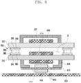
- FIG. 2 is an exploded perspective view of partial configurations of an electronic device according to various embodiments of the disclosure
- FIG. 3 is a combined view of partial configurations of an electronic device according to various embodiments of the disclosure.
- an electronic device 200 may include a housing 201, a first circuit board 210, a second circuit board 220, an interposer 230, a third circuit board 240, a connector 250, a first battery 260, a second battery 262, an antenna module 270, and a back cover 280.
- the electronic device 200 may include the electronic device (at least one of 101, 102, and 104) of FIG. 1 .
- the first battery 260 and the second battery 262 may include the battery 189 of FIG. 1 .
- the antenna module 270 may include the antenna module 197 of FIG. 1 .
- the back cover 280 may be provided on the back of the electronic device 101 of FIG. 1 .
- Each of the first circuit board 210, the second circuit board 220, and the third circuit board 240 may include at least one connection terminal (e.g., a connector) for electrically connecting to other constituent elements.
- Each of the first circuit board 210, the second circuit board 220, and the third circuit board 240 may include a printed circuit board (PCB), a printed board assembly (PBA), and a flexible printed circuit board (FPCB).
- PCB printed circuit board
- PBA printed board assembly
- FPCB flexible printed circuit board
- the housing 201 may be configured in a side bezel structure to accommodate the constituent elements of the electronic device 200 as described above, such as the first circuit board 210, the second circuit board 220, the interposer 230, the third circuit board 240, the connector 250, the first battery 260, the second battery 262, the antenna module 270, and the back cover 280. At least a part of an external exposure surface of the housing 201 may be made of a conductive material (e.g., metal). At least a part of the external exposure surface of the housing 201 may be used as an antenna of the electronic device 200.
- a conductive material e.g., metal
- the housing 201 may include a support member (e.g., a bracket) 203 provided therein.
- the support member 203 may accommodate therein and support constituent elements of the electronic device 200.
- the support member 203 may be integrally formed on one surface of the housing 201.
- the support member 203 may be formed of, for example, a metal material and/or a non-metal material (e.g., polymer).
- the first circuit board 210 may be deployed in at least a part of the housing 201.
- the first circuit board 210 may include a processor (e.g., the processor 120 of FIG. 1 ) required to operate the electronic device 200, a memory (e.g., the memory 130 of FIG. 1 ), a communication circuit (e.g., the communication module 190 of FIG. 1 ), a power management module (e.g., the power management module 188 of FIG. 1 ), and/or an interface (e.g., the interface 177 of FIG. 1 ).
- a processor e.g., the processor 120 of FIG. 1
- a memory e.g., the memory 130 of FIG. 1
- a communication circuit e.g., the communication module 190 of FIG. 1
- a power management module e.g., the power management module 188 of FIG. 1
- an interface e.g., the interface 177 of FIG. 1 .
- the processor may include one or more of a CPU, an AP (e.g., an AP 212 of FIG. 6 ), a call processor (e.g., a call processor 214 of FIG. 6 ), a graphic processor, an ISP, a sensor hub processor, and a CP.
- the memory e.g., the memory 130 of FIG. 1
- the communication circuit e.g., the communication module 190 of FIG. 1
- the interface may include, for example, a HDMI, a USB interface, an SD card interface, and/or an audio interface.
- the interface may electrically or physically connect the electronic device 200 to an external electronic device (e.g., the electronic device 102 of FIG. 1 ), and may include a USB connector, an SD card/MMC connector, or an audio connector.
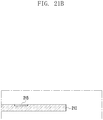
- the second circuit board 220 may be laminated on the first circuit board 210 through the interposer 230.
- the second circuit board 220 may include a transceiver (e.g., a transceiver 221 of FIG. 6 ) or a wireless communication module (e.g., a Wi-Fi module) in which a (e.g., the call processor 214 of FIG. 6 ) and a transceiver are integrated.
- a transceiver e.g., a transceiver 221 of FIG. 6
- a wireless communication module e.g., a Wi-Fi module
- the interposer 230 may be deployed between the first circuit board 210 and the second circuit board 220.
- the interposer 230 may include a space S in which at least one component mounted on the second circuit board 220 (e.g., the AP 212 of FIG. 6 , call processor 214, transceiver 221, and Wi-Fi module) is deployed.
- the interposer 230 may include at least one via 300 for electrically connecting the first circuit board 210 and the second circuit board 220 to each other.
- the third circuit board 240 may further include at least one antenna (e.g., an antenna 275 of FIG. 4 ) for transmitting/receiving a signal or power to/from an outside or a connection terminal connected to the antenna.
- at least one antenna e.g., an antenna 275 of FIG. 4
- the connector 250 may electrically connect the first circuit board 210, the second circuit board 220, and the third circuit board 240 to each other.
- the first battery 260 (e.g., the battery 189 of FIG. 1 ) may supply the power to at least one constituent element of the electronic device 200.
- the second battery 262 may supply the power to at least one constituent element of the electronic device 200.
- the second battery 262 may be an auxiliary battery for increasing the capacity of the first battery 260.
- the second battery 262 may be deployed in a space secured by laminating the first circuit board 210 and the second circuit board 220 through the interposer 230.
- the second battery 262 may be deployed between the second circuit board 220 and the third circuit board 240.
- the connector 250 may electrically connect the second circuit board 220 and the third circuit board 240 to each other, and may be deployed on at least one of an upper portion, a lower portion, and a side portion of the first battery 260 or the second battery 262.
- the first battery 260 and the second battery 262 may include, for example, a non-rechargeable primary cell, a rechargeable secondary cell, or a fuel cell.
- the first battery 260 and the second battery 262 may be integrally deployed in the housing 201 of the electronic device 200, or may be detachably deployed in the housing 201 of the electronic device 200.
- the first battery 260 and the second battery 262 may be configured as one pack.
- the first battery 260 and the second battery 262 may include different fuel gauges for grasping the capacities thereof, or may use different chargers. Through this, the batteries having different sizes can be efficiently managed.
- the first battery 260 and the second battery 262 may be configured as one cell.
- the antenna module 270 may be deployed between the third circuit board 240 and the back cover 280.
- the antenna module 270 (e.g., the antenna module 197 of FIG. 1 ) may be connected to the third circuit board 240.
- the antenna module 270 may include an antenna 275 illustrated in FIG. 4 .
- the third circuit board 240 may include a connection terminal connected to the antenna module 270.
- the antenna module 270 may, for example, communicate with an external device or wirelessly transmit and receive the power necessary for charging.
- an antenna structure may be formed by a partial exposure surface of the housing 201 and/or a part of the support member 203 or a combination thereof.
- the back cover 280 may be a cover for protecting the back surface of the electronic device 200 (e.g., the electronic device 101 of FIG. 1 ).
- FIG. 4 is a perspective view schematically illustrating a connection relationship among first, second, and third circuit boards of an electronic device according to various embodiments of the disclosure
- FIG. 5 is a side view schematically illustrating a connection relationship among first, second, and third circuit boards of an electronic device according to various embodiments of the disclosure.
- an electronic device 200 may include a first circuit board 210, a second circuit board 220, an interposer 230, and a third circuit board 240.
- a communication circuit (e.g., the communication module 190 of FIG. 1 ) may be deployed on the first circuit board 210.
- the communication circuit may include, for example, an AP (e.g., the AP 212 of FIG. 6 ) and a call processor (e.g., the call processor 214 of FIG. 6 ).
- a first connection terminal 310 electrically connected to an output of the communication circuit may be formed on a first surface (e.g., the upper portion) of the first circuit board 210.
- the second circuit board 220 may include, for example, a transceiver (e.g., the transceiver 221 of FIG. 6 ) or a Wi-Fi module.
- a second connection terminal 320 may be deployed on a first surface (e.g., a lower portion) of the second circuit board 220, and a third connection terminal 330 may be deployed on a second surface (e.g., upper portion) of the second circuit board 220.
- the second connection terminal 320 may be electrically connected (e.g., a digital signal) to components (e.g., communication circuit) mounted on the second circuit board 220.
- the third connection terminal 330 may be electrically connected (e.g., an analog signal) to a fourth connection terminal 340 formed on the third circuit board 240.
- the third connection terminal 330 may be connected to the first circuit board 210 through another connection terminal (e.g., a sixth connection terminal (not illustrated)) excluding the first connection terminal 310 formed on the first circuit board 210.
- the third connection terminal 330 connected to the connector 250 may be deployed on the first circuit board 210.
- the third connection terminal 330 may be electrically connected to the first circuit board 210 through another connection member excluding the first connection terminal 310 formed on the first circuit board 210, and thus a signal can be transferred from the second circuit board 220 to the first circuit board 210 through the interposer 230 without a loss.
- the interposer 230 may have different permittivity from that of the first circuit board 210 and the second circuit board 220.
- the second connection terminal 320 of the second circuit board 220 may be electrically connected to a second end portion (e.g., an upper portion) of a via 300, and the second circuit board 220 may be attached to a second surface (e.g., an upper surface) of the interposer 230 in an opposite direction to the a first surface (lower surface) of the interposer 230 so that the second circuit board 220 forms an inner space S together with the first circuit board 210 and the interposer 230.
- the interposer 230 may be deployed between the first circuit board 210 and the second circuit board 220.
- the interposer 230 may have a space S in which at least one component mounted on the second circuit board 220 (e.g., the AP 212 of FIG. 6 , call processor 214, transceiver 221, and Wi-Fi module) is deployed.
- the interposer 230 may be configured in a rectangular shape or in other various shapes.
- the interposer 230 may include at least one via 300 for electrically connecting the first connection terminal 310 formed on the first surface (e.g., an upper surface) of the first circuit board 210 and the second connection terminal 320 formed on the first surface (e.g., a lower surface) of the second circuit board 220 to each other.
- the first surface (e.g., a lower surface) of the interposer 230 may be attached to the first circuit board 210 so that the interposer 230 at least partly surrounds at least a partial region of the first circuit board 210 and the first end portion (e.g., a lower portion) of the via 300 is electrically connected to the first connection terminal 310.
- the fourth connection terminal 340 may be deployed on a first side of the third circuit board 240, and a fifth connection terminal 350 may be deployed on a second side of the third circuit board 240.
- the fourth connection terminal 340 and the fifth connection terminal 350 may be electrically connected to each other.
- the fifth connection terminal 350 formed on the third circuit board 240 may be electrically connected to the antenna 275 (e.g., the antenna module 197 of FIG. 1 ).
- the third connection terminal 330 may be deployed on the first circuit board 210 as a sixth connection terminal (not illustrated). If the sixth connection terminal is deployed on the first circuit board 210, the sixth connection terminal may be electrically connected to the fourth connection terminal 340 formed on the third circuit board 240 through the connector 250.
- the connector 250 may be a FPCB type, coaxial type, or connector type connection member connecting the circuit boards through blocking of a radio frequency (RF) signal.
- RF radio frequency
- the third connection terminal 330 formed on the second surface (e.g., an upper portion) of the second circuit board 220 and the fourth connection terminal 340 formed on the first side of the third circuit board 240 may be electrically connected to each other through the connector 250.
- the third connection terminal 330 may not be limited to be formed on the second circuit board 220.
- the third connection terminal 330 may be deployed on the first circuit board 210 so far as it can minimize a loss through impedance matching by changing the size and/or permittivity of the via 300 formed on the interposer 230.
- the first circuit board 210 may extract raw data by decoding an in-phase signal and a quadrature signal received through a transceiver of the second circuit board 220.
- the second circuit board 220 may separate a RF band and may process analog data including a carrier frequency signal.
- the interposer 230 may transfer a baseband signal that does not include the carrier frequency signal to the first circuit board 210.
- the interposer 230 may process a digital signal including the in-phase signal and the quadrature signal.
- the connector 250 may transfer an analog signal from which the RF band is separated to the fourth connection terminal 340 of the third circuit board 240 through the third connection terminal 330 formed on the second circuit board 220.
- the first circuit board 210 may transfer the digital signal related to the RF band to the second circuit board 220 through the interposer 230.
- the second circuit board 220 may transfer the digital signal related to the RF band to the third circuit board 240, to which the antenna 275 is connected, other than the first circuit board 210.
- the analog signal, from which the RF band that is electrically connected to the antenna 275 is separated may be transferred to the first circuit board 210 through the interposer 230.
- the permittivity of the interposer 230 or the size of the via 300 may be adjusted.
- the analog signal from the interposer 230 may be transferred to the first circuit board 210.
- the transferred analog signal may be transferred to the fourth connection terminal of the third circuit board 240 through another connection terminal on the first circuit board 210.
- the via 300 formed on the interposer 230 may be copied into the connector 250 to calculate the impedance.
- Z 0 denotes impedance
- d1 denotes an inner diameter of a shield pattern surrounding the via 300
- d2 denotes an outer diameter of the via 300
- k denotes relative permittivity
- FIG. 6 is a diagram illustrating a configuration of first to third circuit boards of an electronic device and a connection relationship among them according to various embodiments of the disclosure.
- an electronic device 200 may include a first circuit board 210, a second circuit board 220, an interposer 230, and a third circuit board 240.
- the first circuit board 210 may include, for example, an AP 212, and a call processor 214.
- the first circuit board 210 may include a first connection terminal 310 on a first surface thereof.
- the AP 212 may control functions of constituent elements (e.g., the processor 120, the memory 130, the communication module 190, and the power management module 188 of FIG. 1 ) required to operate the electronic device 200.
- the call processor 214 may modulate and demodulate a signal related to a communication protocol of the electronic device 200.
- the second circuit board 220 may include a transceiver 221, a first filter 222, a power amplifier 223, a switch 224, a second filter 225, and a low-noise amplifier 226.
- a second connection terminal 320 may be deployed on a first surface of the second circuit board 220, and a third connection terminal 330 may be deployed on a second surface of the second circuit board 220.
- the second connection terminal 320 and the third connection terminal 330 may be electrically connected to each other through another component.
- the transceiver 221 may mix a signal modulated through the call processor 214 of the first circuit board 210 with a carrier frequency signal through a mixer to transmit (Tx) the mixed signal, or may separate the receive (Rx) demodulated signal from the carrier frequency signal to modulate the separated signal.
- the first filter 222 may perform matching of the signal transferred from the transceiver 221, or may perform filtering of a noise signal from the carrier frequency signal.
- the power amplifier 223 may amplify the transmit (Tx) signal filtered through the first filter 222 to increase a current gain of the signal.
- the switch 224 may separate paths of the transmit (Tx) signal and the receive (Rx) signal from each other.
- the second filter 225 may perform filtering of the noise signal from the receive (Rx) signal transferred through the switch 224.
- the low-noise amplifier 226 may amplify the receive (Rx) signal transferred through the second filter 225, and may transfer the amplified signal to the transceiver 221.
- the interposer 230 may be deployed between the first circuit board 210 and the second circuit board 220.
- the interposer 230 may include the via 300 for electrically connecting the first connection terminal 310 formed on the first surface of the first circuit board 210 and the second connection terminal 320 formed on the first surface of the second circuit board 220 to each other.
- the third circuit board 240 may include a matching switch 242 controlled through the call processor 214 mounted on the first circuit board 210 and a hall integrated circuit (IC) 244 controlled through the AP 212.
- a control signal provided by the AP 212 and the CP 214 mounted on the first circuit board 210 may be transferred to a separate connection member (e.g., a connector FPCB) electrically connecting the first circuit board 210 and the third circuit board 240 to each other.
- a fourth connection terminal 340 may be deployed on a first side of the third circuit board 240, and a fifth connection terminal 350 may be deployed on a second side of the third circuit board 240.
- the fourth connection terminal 340 and the fifth connection terminal 350 may be electrically connected to each other.
- the fifth connection terminal 350 formed on the third circuit board 240 may be electrically connected to the antenna 275.
- the matching switch 242 may adjust matching of ground (GND) or feeding of the antenna 275 connected to the fifth connection terminal 350 of the third circuit board 240.
- the hall IC 244 may recognize, for example, opening or closing of a mobile terminal having a cover (e.g., a folder phone).
- the antenna 275 may transmit and receive a transmit (Tx) signal and a receive (Rx) signal for a specific wavelength.
- the third connection terminal 330 formed on the second surface of the second circuit board 220 and the fourth connection terminal 340 formed on the first side of the third circuit board 240 may be electrically connected to each other through the connector 250.
- FIG. 7 is a view illustrating a configuration of first and second circuit boards of an electronic device according to various embodiments of the disclosure.
- an electronic device 200 may include a first circuit board 210, a second circuit board 220, an interposer 230, a first shield member 410, and a second shield member 420.
- an AP 212 may be mounted on a lower portion of the first circuit board 210.
- the first shield member 410 may be deployed on an outside of the AP 212 mounted on the lower portion of the first circuit board 210.
- the first shield member 410 may block, for example, a noise signal output from the first circuit board 210 of the electronic device 200, and may block noise input from an outside of the electronic device 200.
- the first shield member 410 may be a shield can or electromagnetic interference (EMI) molding member.
- EMI electromagnetic interference
- the CP 214 may be mounted on an upper portion of the first circuit board 210.
- the CP 214 mounted on the upper portion of the first circuit board 210 may be deployed in a component mount space S in the interposer 230.
- a first connection terminal 310 may be deployed on the first surface (e.g., an upper portion) of the first circuit board 210.
- a second connection terminal 320 may be deployed on the first surface (e.g., a lower portion) of the second circuit board 220.
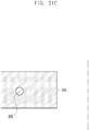
- the interposer 230 may include a via 300, a first pad 302, a second pad 304, and a side plating member 305.
- the via 300 may electrically connect the first connection terminal 310 formed on the first circuit board 210 and the second connection terminal 320 formed on the second circuit board 220 to each other.
- the via 300 may include a through via or a stacked via.
- the first pad 302 may be formed on a lower portion of the via 300 and may be electrically connected to the first connection terminal 310 of the first circuit board 210.
- the second pad 304 may be formed on an upper portion of the via 300 and may be electrically connected to the second connection terminal 320 of the second circuit board 220.
- the side plating member 305 may be provided on an outside of the via 300.
- the side plating member 305 may combine the first circuit board 210 and the second circuit board 220 with each other (e.g., may be electrically connected to the first circuit board 210 or the second circuit board 220), or may support them (may not be electrically connected to the first circuit board 210 or the second circuit board 220).
- the side plating member 305 may be selectively used.
- a transceiver 221 On an upper portion of the second circuit board 220, for example, a transceiver 221 may be mounted.
- the second shield member 420 may be deployed on an outside of the transceiver 221 mounted on the upper portion of the second circuit board 220.
- the second shield member 420 may block, for example, a noise signal output from the second circuit board 220 of the electronic device 200, and may block noise input from an outside of the electronic device 200.
- the second shield member 420 may be a shield can or EMI molding member.
- the EMI molding members of the first shield member 410 and the second shield member 420 may be respectively combined with the first circuit board 210 and the second circuit board 220 through the following process.
- a pad for shield may be formed on at least a part of the lower portion of the first circuit board 210 and on at least a part of the upper portion of the second circuit board 220.
- the first shield member 410 and the second shield member 420 may be mounted on the pad for shield formed on at least the part of the lower portion of the first circuit board 210 and on at least the part of the upper portion of the second circuit board 220.
- non-conductive molding liquid e.g., epoxy molding compound (EMC)
- EMC epoxy molding compound
- the non-conductive molding liquid spread around the pad for shield on which the first shield member 410 and the second shield member 420 are mounted may be etched through laser.
- sputtering of a conductive metal may be performed with respect to the pad for shield and the non-conductive molding liquid.
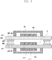
- FIG. 8 is a view illustrating a configuration of first and second circuit boards of an electronic device according to various embodiments of the disclosure.
- an electronic device 200 may include a first circuit board 210, a second circuit board 220, an interposer 230, a first shield member 410, a TIM 412, a heat dissipation member 414, a copper sheet 416, and a second shield member 420.
- an AP 212 may be mounted on a lower portion of the first circuit board 210.
- the first shield member 410 may be deployed on an outside of the AP 212 mounted on the lower portion of the first circuit board 210.
- the first shield member 410 may block, for example, a noise signal output from the first circuit board 210 of the electronic device 200, and may block noise input from an outside of the electronic device 200.
- the first shield member 410 may be a shield can or EMI molding member.
- At least a part of the first shield member 410 may be opened.
- a first end of the thermal interface material (TIM) 412 may be deployed adjacent to the AP 212, and a second end thereof may be provided to penetrate the open part of the first shield member 410.
- the TIM 412 may serve to transfer heat generated from the call processor 214 of the electronic device 200 to the heat dissipation member 414.
- the TIM 412 may be made of a material having a large heat transfer coefficient.
- the copper sheet 416 may be provided between the first end and the second end of the TIM 412. The copper sheet 416 may close the open part of the first shield member 410.
- the copper sheet 416 may block the noise generated inside the electronic device 200.
- the heat dissipation member 414 may be deployed on a support member (e.g., a bracket) 203.
- the heat dissipation member 414 may transfer the heat transferred through the TIM 412 to the support member 203, and may dissipate the heat to outside through the support member 203.
- the call processor 214 may be mounted on an upper portion of the first circuit board 210.
- the call processor 214 mounted on the upper portion of the first circuit board 210 may be deployed in a component mount space S in the interposer 230.
- a first connection terminal 310 may be deployed on the first surface (e.g., an upper portion) of the first circuit board 210.
- a second connection terminal 320 may be deployed on the first surface (e.g., a lower portion) of the second circuit board 220.
- the interposer 230 may include a via 300, a first pad 302, a second pad 304, and a side plating member 305.
- the via 300 may electrically connect the first connection terminal 310 formed on the first circuit board 210 and the second connection terminal 320 formed on the second circuit board 220 to each other.
- the via 300 may include a through via or a stacked via.
- the first pad 302 may be formed on a lower portion of the via 300 and may be electrically connected to the first connection terminal 310 of the first circuit board 210.
- the second pad 304 may be formed on an upper portion of the via 300 and may be electrically connected to the second connection terminal 320 of the second circuit board 220.
- the side plating member 305 may be provided on an outside of the via 300.
- the side plating member 305 may combine the first circuit board 210 and the second circuit board 220 with each other, or may support them.
- the side plating member 305 may be selectively used.
- a transceiver 221 On an upper portion of the second circuit board 220, for example, a transceiver 221 may be mounted.
- the second shield member 420 may be deployed on an outside of the transceiver 221 mounted on the upper portion of the second circuit board 220.
- the second shield member 420 may block, for example, a noise signal output from the second circuit board 220 of the electronic device 200, and may block noise input from an outside of the electronic device 200.
- the second shield member 420 may be a shield can or EMI molding member.
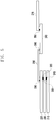
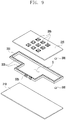
- FIG. 9 is a perspective view schematically illustrating a connection relationship between first and second circuit boards of an electronic device according to various embodiments of the disclosure
- FIG. 10 is a side view schematically illustrating a connection relationship between first and second circuit boards of an electronic device according to various embodiments of the disclosure.
- an electronic device 200 may include a first circuit board 210, a second circuit board 220, and an interposer 230.
- a communication circuit (e.g., 5G RF module) may be deployed on the first circuit board 210.
- a first connection terminal 310 electrically connected to an output of the communication circuit may be formed on a first surface (e.g., an upper portion) of the first circuit board 210.
- an array antenna 285 (e.g., an antenna module 197 of FIG. 1 ) may be arranged on an upper portion of the second circuit board 220.
- a second connection terminal 320 may be deployed on a first surface (e.g., a lower portion) of the second circuit board 220.
- the array antenna 285 and the second connection terminal 320 may be electrically connected to each other.
- electronic components may be mounted only on one surface of the second circuit board 220.
- a third connection terminal e.g., a third connection terminal 330 of FIG. 4
- a c clip that can electrically connect another antenna element may be deployed on a second surface (e.g., an upper portion) of the second circuit board 220.
- the array antenna 285 may be at least one antenna patterned on the second circuit board 220 or a connection member connected to the antenna (e.g., the antenna 275 of FIG. 4 ).
- a third circuit board 240 to which the antenna 275 is connected may not be provided.
- the interposer 230 may be deployed between the first circuit board 210 and the second circuit board 220.
- the interposer 230 may have a space S in which at least one component (e.g., 5G RF module) mounted on the first circuit board 210 is deployed.
- the interposer 230 may be configured in a rectangular shape or in other various shapes.
- the interposer 230 may include at least one via 300 for electrically connecting the first connection terminal 310 formed on the first surface (e.g., an upper surface) of the first circuit board 210 and the second connection terminal 320 formed on the first surface (e.g., a lower surface) of the second circuit board 220 to each other.
- the electronic device 200 may be configured to be able to perform 3D beamforming.
- the second circuit board 220 may include the array antenna 285.
- the interposer 230 may include at least one side plating member 305 provided on the side surface thereof.
- the side plating member 305 may be connected to the array antenna 285.
- the side plating member 305 may operate as a part of the array antenna 285.
- the side plating member 305 may cover three surfaces (e.g., upper, side, and back surfaces) of the interposer 230.
- the side plating member 305 may be in a " ⁇ " shape.
- the electronic device 200 may be configured to transfer an RF signal to the third circuit board 240 through the third connection terminal (e.g., the third connection terminal 330 of FIG. 4 ) after mounting a Wi-Fi module on the second circuit board 220, or to directly connect the antenna (e.g., the antenna 275 of FIG. 4 ) through an antenna connection terminal (fifth connection terminal 350 of FIG. 4 or c clip) formed on the second circuit board 220 without transferring the RF signal to the third circuit board 240.
- the third connection terminal e.g., the third connection terminal 330 of FIG. 4
- the antenna connection terminal e.g., the antenna 275 of FIG. 4
- an antenna connection terminal e.g., the antenna connection terminal 350 of FIG. 4 or c clip
- the AP 212 mounted on the first circuit board 210 may transfer a digital signal for controlling the Wi-Fi module mounted on the second circuit board 220 to the second circuit board 220 through the via 300 of the interposer 230, and the Wi-Fi module on the second circuit board 220 may modulate the digital signal and may directly transfer the RF signal through the antenna 275 that is not the third circuit board 240 through the antenna connection terminal (fifth connection terminal 350 of FIG. 4 or c clip).
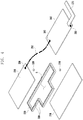
- FIGS. 11 and 12 are views illustrating embodiments of an interposer of an electronic device according to various embodiments of the disclosure.
- an interposer 230 of an electronic device 200 may be composed of a first portion 231 having vias 300 formed thereon, a second portion 232, a third portion 233, and a fourth portion 234, which are integrally connected to each other. Even if the interposer 230 is configured in various different shapes, all portions constituting the interposer 230 may be integrally connected to each other.
- the interposer 230 may include a space S in which at least one component (e.g., the AP 212, call processor 214, or transceiver 221) mounted on the second circuit board 220 is deployed.
- an electronic device 200 may be provided with at least one interposer 230.
- the interposer 230 may include a first portion (e.g., first interposer) 231 having vias 300 formed thereon, a second portion (e.g., first interposer) 232, a third portion (e.g., first interposer) 233, and a fourth portion (e.g., first interposer) 234, which can be separated from each other through first to fourth slits s1 to s4.
- the first portion 231 and the second portion 232 may be separated from each other by the first slit s1.
- the second portion 232 and the third portion 233 may be separated from each other by the second slit s2.
- the third portion 233 and the fourth portion 234 may be separated from each other by the third slit s3.
- the fourth portion 234 and the first portion 231 may be separated from each other by the fourth slit s4.
- the first to fourth slits s1 to s4 may be configured enough to prevent inflow of a noise signal from outside.
- the first to fourth slits s1 to s4 may be configured at an interval that is smaller than the electrical wavelength of the noise signal from the outside.
- the interposer 230 may further include a shield member for shielding partial components in an inner space S.
- the shield member may be a shield can or EMI molding member.
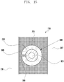
- FIG. 13 is a view illustrating a via and an interposer of an electronic device according to various embodiments of the disclosure.
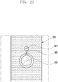
- a via 300 of an electronic device 200 may be composed of a through via.
- the via (e.g., through via) 300 may include a hole 301, a plating pad 303, and an insulation region 306.
- the hole 301 may be formed to penetrate, for example, at least a part of an interposer 230 through a drill.
- An inner wall of the hole 301 may be plated to transfer an electrical signal.
- the plating pad 303 (e.g., the first pad 302 or second pad 304 of FIG. 7 ) may be formed to surround an outer side of the hole 301.
- the plating pad 303 may be composed of a copper film and a gold film.
- the gold film may correspond to gold plating performed to prevent corrosion of the copper film.
- the insulation region 306 may be formed to surround an outer side of the plating pad 303.
- the insulation region 306 may be, for example, a region in which the copper film is opened so that the plating pad 303 of the via 300 is not connected to another signal (e.g., a ground region 235) of the interposer 230. Only solder resist (SR) ink may be spread on the region in which the copper film is open.
- SR solder resist
- the interposer 230 of the electronic device 200 may include a ground region 235, a first keep-out region 236, and a second keep-out region 237.
- the ground region 235 may surround or may be electrically connected to at least a part (e.g., the insulation region 306) of the via 300.
- the ground region 235 may be composed of a copper film and SR ink.
- the SR ink may be ink spread to prevent corrosion of the copper film.
- the first keep-out region 236 may be formed on the first side of the ground region 235.
- the second keep-out region 237 may be formed on the second side of the ground region 235.
- the first keep-out region 236 and the second keep-out region 237 may be formed on both sides of the ground region 235.
- the first keep-out region 236 or the second keep-out region 237 may be a region in which an interconnect formed based on an error that is necessary for routing to cut an outline of the interposer 230 in a desired shape does not exist.
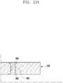
- FIG. 14 is a view illustrating a via and an interposer of an electronic device according to various embodiments of the disclosure.
- a via 300 of an electronic device 200 may be composed of a tacked via.
- the via (e.g., stacked via) 300 may include an inner via 307, a plating pad 303, and an insulation region 306.
- the inner via 307 may be formed to be smaller than the plating pad 303 (e.g., the first pad 302 or second pad 304 of FIG. 7 ) for high-speed signal movement.
- the plating pad 303 may surround an outer side of the inner via 307.
- the plating pad 303 may close an end portion of the inner via 307.
- the plating pad 303 may be composed of a copper film and a gold film.
- the gold film may correspond to gold plating performed to prevent corrosion of the copper film.
- the insulation region 306 may be formed to surround an outer side of the plating pad 303.
- the insulation region 306 may be, for example, a region in which the copper film is opened so that the plating pad 303 of the via 300 is not connected to another signal (e.g., the ground region 235) of the interposer 230. Only SR ink may be spread on the region in which the copper film is open.
- the interposer 230 of the electronic device 200 may include a ground region 235, a first keep-out region 236, and a second keep-out region 237.
- the interposer 230 illustrated in FIG. 14 may have the same configuration as the configuration of the interposer 230 illustrated in FIG. 13 .
- FIG. 15 is a view illustrating a via and an interposer of an electronic device according to various embodiments of the disclosure.
- a via 300 of an electronic device 200 may be composed of a through via.
- the via (e.g., through via) 300 may include a hole 301, a plating pad 303, and an insulation region 306.
- the via 300 illustrated in FIG. 15 may have the same configuration as the configuration of the via 300 illustrated in FIG. 13 .
- the interposer 230 illustrated in FIG. 15 may have the same configuration as the configuration of the interposer 230 illustrated in FIG. 13 .
- the configuration illustrated in FIG. 15 is different from the configuration illustrated in FIG. 13 on the point that the ground region 235 of the interposer 230 and the plating pad of the via 300 can be connected to each other using an interconnect 309.
- FIG. 16 is a view illustrating a configuration of an interposer of an electronic device according to various embodiments of the disclosure.
- an interposer 230 of an electronic device 200 may be configured so that a part (e.g., an inner side) of a ground region 235 is removed, and the width of the interposer 230 is reduced as much as the removed ground region 235.
- FIG. 17 is a view illustrating a configuration of an interposer of an electronic device according to various embodiments of the disclosure.
- an interposer 230 of an electronic device 200 may include different vias (e.g., stacked via and through via) 300.
- the interposer 230 may be configured so that a part (e.g., an outer side) of a ground region 235 is removed, and a side plating member 305 is deployed in the removed region and a first keep-out region 236.
- the side plating member 305 may cover three surfaces (e.g., upper, side, and back surfaces) of the interposer 230.
- the side plating member 305 may be in a " ⁇ " shape.
- the interposer 230 may be configured so that a part (e.g., an inner side) of the ground region 235 is removed, and the side plating member 305 is deployed in the removed region and a second keep-out region 237.
- the first and second keep-out regions 236 and 237 may be regions in which an interconnect formed based on an error that is necessary for routing to cut an outline of the interposer 230 in a desired shape does not exist.
- the side plating member 305 is formed in the first and second keep-out regions 236 and 237 through a separate addition process (e.g., drilling, copper plating, and gold plating in the first and second keep-out regions 236 and 237 of the side surface of the interposer 230 after the routing), and thus the existing unused space can be utilized.
- a separate addition process e.g., drilling, copper plating, and gold plating in the first and second keep-out regions 236 and 237 of the side surface of the interposer 230 after the routing
- the width of the interposer 230 can be reduced as large as a part of the width of the removed ground region 235.
- the side plating members deployed on the outer side and the inner side of the interposer 230 may be deployed in parallel locations or may be deployed to cross each other in a zigzag shape.
- the side plating member 305 may be integrally connected to the via 300.
- the side plating member 305 may be connected to the via 300 through the interconnect 309.
- the side plating member 305 may be connected to the array antenna 285 illustrated in FIG. 9 and may operate as a part of the antenna.
- the side plating member 305 may be connected to the ground region 235 through an extension part extending from the ground region 235.
- the side plating member 305 connected to the via 300 and the ground region 235 may serve as a shield member blocking noise input from an outside of the electronic device 200.
- FIG. 18 is a view illustrating a configuration of an interposer of an electronic device according to various embodiments of the disclosure.
- an interposer 230 of an electronic device 200 may include different vias (e.g., through via and stacked via) 300.
- the interposer 230 illustrated in FIG. 18 may be configured so that a ground region 235 surrounding the via 300 is not formed. Through this, the width of the interposer 230 can be reduced as large as the removed ground region 235.
- the ground region 235 can be deleted. If the ground region 235 is not formed in the interposer 230, the interposer 230 may be made of a shield can or EMI molding material that is a shield structure.
- ground region 235 if the ground region 235 is not formed in the interposer 230, components deployed in an inner space of the interposer 230 or outside the interposer 230 may be shielded through shield can or EMI molding that is a shield structure, and may replace the noise shielding of the removed ground region 235.
- FIG. 19 is a view illustrating a configuration of an interposer, a via, and a side plating member of an electronic device according to various embodiments of the disclosure.
- an interposer 230 of an electronic device 200 may include different vias (e.g., through via and stacked via) deployed in a zigzag shape.
- the interposer 230 may have the different vias (e.g., through via and stacked via) deployed in a straight line.
- the interposer 230 may have the same vias (e.g., through vias or stacked vias) deployed in a zigzag shape.
- the interposer 230 may have the same vias (e.g., through vias or stacked vias) deployed in a straight line.
- a plurality of side plating members 305 may be deployed in a zigzag shape in the interposer 230.
- the side plating member 305 formed on an outer side of the interposer 230 may block inflow of a noise signal from an outside of the electronic device 200.
- the side plating member 305 formed on an inner side of the interposer 230 may block a noise signal output from the inside of the electronic device 200 (e.g., the first circuit board 210 and/or second circuit board 220).
- the via 300 can be moved adjacent to the first and second keep-out regions 236 and 237, and thus the width of the interposer 230 can be reduced.
- an opposite space occurring through the movement of the via 300 is secured as a space in which the side plating member 305 can be generated, it can also serve to shield the inner and outer portions of the interposer 230 as well as reducing the width of the interposer 230.
- FIGS. 20A to 20C illustrate a configuration of a via, an interposer, and a first circuit board of an electronic device according to various embodiments of the disclosure.
- FIG. 20A is a cross-sectional view of a via formed in an interposer according to various embodiments of the disclosure
- FIG. 20B is a cross-sectional view illustrating the configuration of a third conduction pad formed on a first circuit board (or second circuit board) according to various embodiments of the disclosure
- FIG. 20C is a plan view illustrating the configuration of a third conduction pad formed on a first circuit board (or second circuit board) according to various embodiments of the disclosure.
- an interposer 230 may include a via (e.g., through via of FIG. 13 ) 300.
- the via 300 may include a hole 301, a first pad 302, and a second pad 304.
- the hole 301 may be formed to penetrate, for example, at least a part of the interposer 230 through a drill.
- the first pad 302 (e.g., first pad 302 of FIG. 7 ) and the second pad 304 (e.g., second pad 304 of FIG. 7 ) may be formed to surround an outer side of the hole 301.
- the first pad 302 may be exposed through a lower portion of the interposer 230.
- the second pad 304 may be exposed through an upper portion of the interposer 230.
- the first pad 302 and the second pad 304 may be composed of a copper film and a gold film.
- the first pad 302 may be electrically connected to a first connection terminal 310 deployed on a first circuit board 210.
- the second pad 304 may be electrically connected to a second connection terminal 320 deployed on a second circuit board 220.
- a third pad 215 may be deployed to strengthen connectivity with the first pad 302 of the via 300 formed in the interposer 230.
- the third pad 215 may be deployed in a location corresponding to the first pad 302 of the via 300.
- a non-plating region 216 may be included inside the third pad 215 deployed on the first circuit board 210.
- the non-plating region 216 may be deployed in a location corresponding to the hole 301 of the via 300.
- the area of the non-plating region 216 may be equal to or larger than the area of the hole 301 so that soldering liquid spread on the third pad 315 is prevented from flowing into the hole 301 of the via 300 during application of surface mount devices (SMD) or surface mount technology (SMT), which is the surface mount technology for connecting the first pad 302 of the interposer 230 and the third pad 215 of the first circuit board 210 to each other.
- the third pad 215 deployed on the first circuit board 210 may also be deployed on the second circuit board 220.
- FIGS. 21A to 21C illustrate a configuration of a via, an interposer, and a first circuit board of an electronic device according to various embodiments of the disclosure.
- FIG. 21A is a cross-sectional view of a via formed in an interposer according to various embodiments of the disclosure
- FIG. 21B is a cross-sectional view illustrating the configuration of a third conduction pad formed on a first circuit board (or second circuit board) according to various embodiments of the disclosure
- FIG. 21C is a plan view illustrating the configuration of a third conduction pad formed on a first circuit board (or second circuit board) according to various embodiments of the disclosure.
- an interposer 230 may include a via (e.g., stacked via of FIG. 14 ) 300.
- the via 300 may include an inner via 307, a first pad 302, and a second pad 304.
- the inner via 307 may be formed to be smaller than the first pad 302 and/or the second pad 304 for high-speed signal movement.
- the first pad 302 (e.g., first pad 302 of FIG. 7 ) and the second pad 304 (e.g., second pad 304 of FIG. 7 ) may close an upper portion and a lower portion of the inner via 307.
- the first pad 302 may be exposed through a lower portion of the interposer 230.
- the second pad 304 may be exposed through an upper portion of the interposer 230.
- the first pad 302 and the second pad 304 may be composed of a copper film and a gold film.
- the first pad 302 may be electrically connected to a first connection terminal 310 deployed on a first circuit board 210.
- the second pad 304 may be electrically connected to a second connection terminal 320 deployed on a second circuit board 220.
- a third pad 215 may be deployed to strengthen connectivity with the first pad 302 of the via 300 formed in the interposer 230.
- the third pad 215 may be deployed in a location corresponding to the first pad 302 of the via 300.
- the third pad 215 deployed on the first circuit board 210 may also be deployed on the second circuit board 220.
- FIG. 22 is a side view illustrating a configuration of an interposer and a side plating member of an electronic device according to various embodiments of the disclosure.
- a side plating member 305 may include a first surface (e.g., a lower surface) 305a, a second surface (e.g., a side surface) 305b, and a third surface (e.g., an upper surface) 305c.
- the side plating member 305 may cover three surfaces (e.g., upper, side, and back surfaces) of the interposer 230.
- the side plating member 305 may be in a " ⁇ " shape.
- the side plating member 305 formed on the interposer 230 may block inflow of a noise signal from an outside of the electronic device 200.
- the side plating member 305 may block a noise signal output from the inside of the electronic device 200 (e.g., the first circuit board 210 and/or second circuit board 220).
- the side plating member 305 may be connected to the array antenna 285 illustrated in FIG. 9 and may operate as a part of the antenna.
- FIG. 23 is a view illustrating a configuration of a via of an electronic device according to various embodiments of the disclosure.
- an interposer 230 may include an inner via 307, an interconnect 309, and a plating pad 303.
- the inner via 307 and the plating pad 303 may be formed in different regions of the interposer 230.
- the inner via 307 and the plating pad 303 may be connected to each other using the interconnect 309.
- the inner via 307 may be SR-processed so as not to be exposed to an outside, and may exist to be separated from the ground region 235.
- interconnects may exist in the interposer 230 in addition to the vias directly connected to each other in a straight line, and thus flexibility of the interconnects can be heightened.
Landscapes
- Engineering & Computer Science (AREA)
- Theoretical Computer Science (AREA)
- Computer Hardware Design (AREA)
- General Engineering & Computer Science (AREA)
- Physics & Mathematics (AREA)
- General Physics & Mathematics (AREA)
- Signal Processing (AREA)
- Human Computer Interaction (AREA)
- Microelectronics & Electronic Packaging (AREA)
- Power Engineering (AREA)
- Computer Networks & Wireless Communication (AREA)
- Electromagnetism (AREA)
- Telephone Set Structure (AREA)
- Combinations Of Printed Boards (AREA)
- Production Of Multi-Layered Print Wiring Board (AREA)
Claims (12)
- Elektronisches Gerät (101, 102, 104, 200) das Folgendes umfasst:eine erste Leiterplatte (210), auf der ein erster Verbindungsanschluss (310) ausgebildet ist;eine erste elektronische Komponente, die mit dem ersten Verbindungsanschluss (310) verbunden ist und auf der ersten Leiterplatte (210) angeordnet ist;einen Interposer (230) mit einer darin ausgebildeten Durchkontaktierung (300) und einer an der ersten Leiterplatte angebrachten ersten Oberfläche, wobei der Interposer wenigstens einen Teilbereich der ersten Leiterplatte (210) wenigstens zum Teil umgibt und ein erster Endabschnitt der Durchkontaktierung elektrisch mit dem ersten Verbindungsanschluss (310) verbunden ist,wobei der Interposer (230) einen wenigstens einen Teil der Durchkontaktierung (300) umgebenden Erdungsbereich (235) umfasst;eine zweite Leiterplatte (220), die einen darin ausgebildeten zweiten Verbindungsanschluss (320) aufweist und in einer der ersten Oberfläche gegenüber liegenden Richtung an einer zweiten Oberfläche des Interposers angebracht ist, wobei der zweite Verbindungsanschluss elektrisch mit einem zweiten Endabschnitt der Durchkontaktierung (300) verbunden ist und die zweite Leiterplatte (220) zusammen mit der ersten Leiterplatte (210) und dem Interposer (230) einen Innenraum bildet;eine zweite elektronische Komponente, die mit dem zweiten Verbindungsanschluss (320) verbunden ist und auf der zweiten Leiterplatte (220) angeordnet ist; undeine Antenne (285), der mit der zweiten elektronischen Komponente elektrisch verbunden ist;wobei der Interposer (230) weiterhin ein Seitenbeschichtungselement (305) aufweist, und wobei das Seitenbeschichtungselement auf einer oberen Fläche, einer Seitenfläche und einer unteren Oberfläche des Interposers auf Ausschlussbereichen (236, 237) ausgebildet ist, die Bereichen des Interposers entsprechen, in denen ein Teil des Erdungsbereichs (235) entfernt wurde, wobei das Seitenbeschichtungselement (305) und die Durchkontaktierung (300) über ein Kontaktelement (309) miteinander verbunden sind, und wobei das Seitenbeschichtungselement (305) über einen Verlängerungsteil (308), der sich von dem Erdungsbereich (235) erstreckt, mit dem Erdungsbereich (235) verbunden ist.
- Elektronisches Gerät (101, 102, 104, 200) nach Anspruch 1, wobei es sich bei der ersten elektronischen Komponente um einen Anwendungsprozessor (AP) handelt und bei der zweiten elektronischen Komponente um einen Kommunikationsprozessor (CP).
- Elektronisches Gerät (101, 102, 104, 200) nach Anspruch 1 oder 2, wobei ein dritter Verbindungsanschluss (330), der elektrisch mit dem zweiten Verbindungsanschluss (320) verbunden ist, an einem oberen Abschnitt der zweiten Leiterplatte (220) ausgebildet ist.
- Elektronisches Gerät (101, 102, 104, 200) nach Anspruch 3, das weiterhin eine dritte Leiterplatte (240) umfasst, die einen darin ausgebildeten vierten Verbindungsanschluss und einen darin ausgebildeten fünften Verbindungsanschluss aufweist, der mit dem vierten Verbindungsanschluss (340) elektrisch verbunden ist, wobei der fünfte Verbindungsanschluss elektrisch mit der Antenne verbunden ist.
- Elektronisches Gerät (101, 102, 104, 200) nach Anspruch 4, das weiterhin einen Verbinder umfasst, der den dritten Verbindungsanschluss (330) und den vierten Verbindungsanschluss (340) elektrisch miteinander verbindet.
- Elektronisches Gerät (101, 102, 104, 200) nach Anspruch 4 oder 5,
wobei ein Akku (189, 260, 262) zwischen der zweiten Leiterplatte (220) und der dritten Leiterplatte angeordnet ist, und wobei ein Abschirmungselement auf einer zweiten Oberfläche der ersten Leiterplatte eingesetzt ist. - Elektronisches Gerät (101, 102, 104, 200) nach einem der vorhergehenden Ansprüche,
wobei ein erstes Pad (302), das elektrisch mit dem ersten Verbindungsanschluss der ersten Leiterplatte verbunden ist, an einem unteren Abschnitt der Durchkontaktierung ausgebildet ist, und wobei ein zweites Pad (304), das elektrisch mit dem zweiten Verbindungsanschluss der zweiten Leiterplatte verbunden ist, an einem oberen Abschnitt der Durchkontaktierung ausgebildet ist. - Elektronisches Gerät (101, 102, 104, 200) nach einem der vorhergehenden Ansprüche,
wobei die zweite Leiterplatte (220) eine dritte Oberfläche umfasst, die mit dem Interposer in Kontakt kommt, und eine vierte Oberfläche umfasst, die in einer der dritten Oberfläche gegenüber liegenden Richtung ausgebildet ist, und
wobei ein Abschirmungselement (420) auf der vierten Oberfläche der zweiten Leiterplatte angeordnet ist. - Elektronisches Gerät (101, 102, 104, 200) nach einem der vorhergehenden Ansprüche,
wobei der Interposer (230) einen ersten Abschnitt (231) mit darin ausgebildeten Durchkontaktierungen (300), einen zweiten Abschnitt (232), einen dritten Abschnitt (233) und einen vierten Abschnitt (234) enthalten kann, die durch einen ersten bis vierten Schlitz (S1 bis S4) voneinander getrennt werden können. - Elektronisches Gerät (101, 102, 104, 200) nach einem der vorhergehenden Ansprüche, wobei die Durchkontaktierung (300) Folgendes umfasst:ein Loch, das derart ausgebildet ist, dass es wenigstens durch einen Teil des Interposers (230) hindurch geht;ein Beschichtungspad (303), das wenigstens einen Teil des Lochs umgibt; undeinen Isolierungsbereich (306), der wenigstens einen Teil des Beschichtungspads (303) umgibt.
- Elektronisches Gerät (101, 102, 104, 200) nach einem der vorhergehenden Ansprüche 1 bis 9, wobei die Durchkontaktierung Folgendes umfasst:eine innere Durchkontaktierung (300), die dazu konfiguriert ist, ein elektrisches Signal zu übertragen;ein Beschichtungspad (303), das wenigstens einen Teil der inneren Durchkontaktierung umgibt; undeinen Isolierungsbereich (306), der wenigstens einen Teil des Beschichtungspads umgibt.
- Elektronisches Gerät (101, 102, 104, 200) nach einem der vorhergehenden Ansprüche, wobei der Interposer Folgendes umfasst:einen ersten Ausschlussbereich (236), der auf einer ersten Seite des Erdungsbereichs auf einer ersten Seite des Interposers ausgebildet ist und der kein Kontaktelement darin aufweist; undeinen zweiten Ausschlussbereich, der auf einer zweiten Seite des Erdungsbereichs auf einer zweiten Seite des Interposers ausgebildet ist und der kein Kontaktelement darin aufweist.
Priority Applications (1)
| Application Number | Priority Date | Filing Date | Title |
|---|---|---|---|
| EP20180231.1A EP3734948B1 (de) | 2017-09-12 | 2018-09-05 | Elektronische vorrichtung mit interposer |
Applications Claiming Priority (1)
| Application Number | Priority Date | Filing Date | Title |
|---|---|---|---|
| KR1020170116517A KR102400748B1 (ko) | 2017-09-12 | 2017-09-12 | 인터포저를 포함하는 전자 장치 |
Related Child Applications (1)
| Application Number | Title | Priority Date | Filing Date |
|---|---|---|---|
| EP20180231.1A Division EP3734948B1 (de) | 2017-09-12 | 2018-09-05 | Elektronische vorrichtung mit interposer |
Publications (2)
| Publication Number | Publication Date |
|---|---|
| EP3454533A1 EP3454533A1 (de) | 2019-03-13 |
| EP3454533B1 true EP3454533B1 (de) | 2020-06-24 |
Family
ID=63682971
Family Applications (2)
| Application Number | Title | Priority Date | Filing Date |
|---|---|---|---|
| EP20180231.1A Active EP3734948B1 (de) | 2017-09-12 | 2018-09-05 | Elektronische vorrichtung mit interposer |
| EP18192713.8A Active EP3454533B1 (de) | 2017-09-12 | 2018-09-05 | Elektronische vorrichtung mit interposer |
Family Applications Before (1)
| Application Number | Title | Priority Date | Filing Date |
|---|---|---|---|
| EP20180231.1A Active EP3734948B1 (de) | 2017-09-12 | 2018-09-05 | Elektronische vorrichtung mit interposer |
Country Status (7)
| Country | Link |
|---|---|
| US (6) | US10674607B2 (de) |
| EP (2) | EP3734948B1 (de) |
| JP (1) | JP7286286B2 (de) |
| KR (1) | KR102400748B1 (de) |
| CN (2) | CN109495612B (de) |
| MY (1) | MY205612A (de) |
| WO (1) | WO2019054679A1 (de) |
Families Citing this family (60)
| Publication number | Priority date | Publication date | Assignee | Title |
|---|---|---|---|---|
| US10527487B2 (en) | 2016-05-31 | 2020-01-07 | Future Technologies In Sport, Inc. | System and method for sensing high-frequency vibrations on sporting equipment |
| US10490511B2 (en) * | 2017-06-01 | 2019-11-26 | Mediatek Inc. | Microelectronic assembly with electromagnetic shielding |
| JP6820297B2 (ja) * | 2018-07-31 | 2021-01-27 | 矢崎総業株式会社 | コネクタ付き回路体、及び、バスバモジュール |
| KR102550209B1 (ko) | 2018-09-19 | 2023-06-30 | 삼성전자주식회사 | 인쇄 회로 기판에 배치된 회로 소자를 둘러싸는 인터포저를 포함하는 전자 장치 |
| WO2020090230A1 (ja) * | 2018-11-01 | 2020-05-07 | 株式会社村田製作所 | 高周波モジュールおよび通信装置 |
| KR102823716B1 (ko) | 2019-02-19 | 2025-06-23 | 삼성전자 주식회사 | 인터포저를 이용한 인쇄 회로 기판 적층 구조 및 그것을 포함하는 전자 장치 |
| CN109874228A (zh) * | 2019-03-28 | 2019-06-11 | 联想(北京)有限公司 | 电子设备 |
| KR102609138B1 (ko) * | 2019-04-29 | 2023-12-05 | 삼성전기주식회사 | 인쇄회로기판 어셈블리 |
| US10681832B1 (en) | 2019-06-06 | 2020-06-09 | Hewlett Packard Enterprise Development Lp | High-density universally-configurable system board architecture with dual-use modular mid-board optics (MBOs) |
| WO2021002271A1 (ja) * | 2019-07-03 | 2021-01-07 | 株式会社村田製作所 | 高周波モジュール及び通信装置 |
| KR102796767B1 (ko) | 2019-07-10 | 2025-04-16 | 삼성전자주식회사 | 인터포저를 포함하는 전자 장치 |
| US11711892B2 (en) * | 2019-07-15 | 2023-07-25 | Velvetwire Llc | Method of manufacture and use of a flexible computerized sensing device |
| KR102659556B1 (ko) | 2019-07-17 | 2024-04-23 | 삼성전자 주식회사 | 인터포저를 포함하는 전자 장치 |
| KR102800074B1 (ko) | 2019-07-22 | 2025-04-28 | 삼성전자주식회사 | 기판 조립체를 포함하는 전자 장치 |
| KR102736631B1 (ko) * | 2019-07-23 | 2024-12-02 | 삼성전자주식회사 | 인터포저 및 이를 포함하는 전자 장치 |
| KR102758032B1 (ko) * | 2019-08-02 | 2025-01-21 | 삼성전자주식회사 | Fpcb를 포함하는 전자 장치 |
| KR102650029B1 (ko) | 2019-08-07 | 2024-03-22 | 삼성전자주식회사 | 센서를 포함하는 전자 장치 |
| KR20210020667A (ko) * | 2019-08-16 | 2021-02-24 | 삼성전자주식회사 | 비아 집단 패턴이 형성된 pcb 임베디드 필터를 포함하는 장치 및 인쇄 회로 기판 |
| KR102659482B1 (ko) * | 2019-09-27 | 2024-04-23 | 삼성전자주식회사 | 인터포저를 포함하는 전자 장치 |
| KR102661196B1 (ko) | 2019-11-08 | 2024-04-29 | 삼성전자 주식회사 | 적층형 기판을 포함하는 전자 장치 |
| KR102801548B1 (ko) | 2020-02-10 | 2025-04-29 | 삼성전자주식회사 | 인쇄 회로 기판에 인터포저를 사용하는 전자 장치 |
| KR102899638B1 (ko) * | 2020-02-11 | 2025-12-15 | 삼성전자주식회사 | 인쇄회로기판 조립체 및 이를 포함하는 전자 장치 |
| KR102823728B1 (ko) * | 2020-02-26 | 2025-06-24 | 삼성전자 주식회사 | 인터포저를 포함하는 전자 장치 |
| EP4096372A4 (de) * | 2020-02-26 | 2023-10-11 | Samsung Electronics Co., Ltd. | Elektronische vorrichtung mit interposer |
| US11108151B1 (en) * | 2020-03-02 | 2021-08-31 | Enlighted, Inc. | Device and method for managing communications |
| CN113573473A (zh) * | 2020-04-28 | 2021-10-29 | 富泰华工业(深圳)有限公司 | 电路板组件及电子装置 |
| KR102832194B1 (ko) * | 2020-06-03 | 2025-07-09 | 삼성전자주식회사 | 인터포저를 포함하는 전자 장치 |
| KR102886443B1 (ko) * | 2020-08-18 | 2025-11-17 | 삼성전자주식회사 | 회로 기판 모듈 및 이를 포함하는 전자 장치 |
| CN112054282A (zh) * | 2020-08-31 | 2020-12-08 | 瑞声新能源发展(常州)有限公司科教城分公司 | 天线结构及移动终端 |
| CN112054281A (zh) * | 2020-08-31 | 2020-12-08 | 瑞声新能源发展(常州)有限公司科教城分公司 | 天线结构及移动终端 |
| US12022614B2 (en) | 2020-09-28 | 2024-06-25 | Samsung Electronics Co., Ltd. | Interposer and electronic device including the same |
| KR102848768B1 (ko) * | 2020-09-28 | 2025-08-21 | 삼성전자 주식회사 | 플렉서블 디스플레이 및 인쇄 회로 기판을 포함하는 전자 장치 |
| KR102864054B1 (ko) | 2020-10-23 | 2025-09-24 | 삼성전자주식회사 | 인터포저를 포함하는 안테나 구조 및 이를 포함하는 전자 장치. |
| KR102876737B1 (ko) * | 2020-11-18 | 2025-10-27 | 삼성전자주식회사 | 인쇄 회로 기판 구조 및 이를 포함하는 전자 장치 |
| CN121726742A (zh) * | 2020-11-30 | 2026-03-24 | 三星电子株式会社 | 包括加固构件的电子设备 |
| KR102889352B1 (ko) | 2020-12-04 | 2025-11-21 | 삼성전자주식회사 | 안테나 및 인쇄회로기판을 포함하는 전자 장치 |
| EP4195630B1 (de) | 2020-12-16 | 2025-02-12 | Samsung Electronics Co., Ltd. | Elektronische vorrichtung |
| KR102902360B1 (ko) * | 2020-12-16 | 2025-12-22 | 삼성전자주식회사 | 전자 장치 |
| WO2022138990A1 (ko) * | 2020-12-21 | 2022-06-30 | 엘지전자 주식회사 | 기판 적층 구조체 및 인터포저 블록 |
| KR102848288B1 (ko) * | 2020-12-24 | 2025-08-20 | 삼성전자주식회사 | 방열 구조를 포함하는 전자 장치 |
| CN112632900B (zh) * | 2020-12-30 | 2024-09-24 | 深圳市百能信息技术有限公司 | Pcb盘中孔自动识别方法、装置、设备及存储介质 |
| CN116648929A (zh) * | 2020-12-31 | 2023-08-25 | 三星电子株式会社 | 包括扬声器的电子装置 |
| US11848279B2 (en) * | 2021-01-12 | 2023-12-19 | Samsung Electronics Co., Ltd. | Electronic device including printed circuit board having shielding structure |
| EP4224282A4 (de) * | 2021-01-12 | 2024-04-17 | Samsung Electronics Co., Ltd. | Elektronische vorrichtung mit mikrofonmodul |
| KR102926797B1 (ko) * | 2021-01-14 | 2026-02-12 | 삼성전자주식회사 | 안테나를 포함하는 전자 장치 |
| CN113438810A (zh) * | 2021-05-18 | 2021-09-24 | 深圳市致趣科技有限公司 | 连接器制作方法、电子设备、连接器及应用 |
| KR102880852B1 (ko) * | 2021-05-21 | 2025-11-04 | 삼성전자주식회사 | 전자 장치 |
| US12021290B2 (en) | 2021-07-20 | 2024-06-25 | Apple Inc. | Radio-frequency transmission line structures for wireless circuitry based on conductive traces on multiple printed circuits |
| KR102938612B1 (ko) * | 2021-08-17 | 2026-03-12 | 삼성전자주식회사 | 인터포저 및 이를 포함하는 전자 장치 |
| EP4351286A4 (de) | 2021-08-17 | 2024-11-20 | Samsung Electronics Co., Ltd. | Interposer und elektronische vorrichtung damit |
| WO2023090626A1 (ko) * | 2021-11-19 | 2023-05-25 | 삼성전자주식회사 | 기판 모듈을 포함하는 전자 장치 |
| CN217217080U (zh) * | 2021-12-08 | 2022-08-16 | 荣耀终端有限公司 | 电子组件及电子设备 |
| CN117156023A (zh) * | 2022-05-24 | 2023-12-01 | 华为技术有限公司 | 一种电子设备 |
| US12278172B2 (en) * | 2022-06-28 | 2025-04-15 | Applied Materials, Inc. | Substrate frame design for three-dimensional stacked electronic assemblies and method for the same |
| JP2024015462A (ja) * | 2022-07-20 | 2024-02-02 | 古河ネットワークソリューション株式会社 | 光デバイス |
| CN119604832A (zh) * | 2022-08-03 | 2025-03-11 | 三星电子株式会社 | 包括围绕电池的带的电子装置 |
| US12369279B2 (en) | 2022-09-30 | 2025-07-22 | Western Digital Technologies, Inc. | Non-planar antennas for portable storage devices |
| US20240121882A1 (en) * | 2022-10-10 | 2024-04-11 | Meta Platforms Technologies, Llc | Thermoplastic interposer |
| WO2024253364A1 (ko) * | 2023-06-05 | 2024-12-12 | 삼성전자 주식회사 | 인터포저를 포함하는 전자 장치 |
| CN121665444A (zh) * | 2024-09-05 | 2026-03-13 | 荣耀终端股份有限公司 | 一种电路板组件及电子设备 |
Family Cites Families (52)
| Publication number | Priority date | Publication date | Assignee | Title |
|---|---|---|---|---|
| GB8412674D0 (en) * | 1984-05-18 | 1984-06-27 | British Telecomm | Integrated circuit chip carrier |
| US5956835A (en) * | 1994-10-03 | 1999-09-28 | Aksu; Allen | Test fixtures for testing of printed circuit boards |
| JP3681542B2 (ja) | 1998-07-01 | 2005-08-10 | 富士通株式会社 | プリント回路基板および多段バンプ用中継基板 |
| GB0012420D0 (en) | 2000-05-24 | 2000-07-12 | Ibm | Microcard interposer |
| US6404043B1 (en) * | 2000-06-21 | 2002-06-11 | Dense-Pac Microsystems, Inc. | Panel stacking of BGA devices to form three-dimensional modules |
| US6670559B2 (en) * | 2000-12-13 | 2003-12-30 | International Business Machines Corp. | Electromagnetic shield for printed circuit boards |
| EP1235471A1 (de) * | 2001-02-27 | 2002-08-28 | STMicroelectronics Limited | Stapelelement |
| US20040156177A1 (en) * | 2003-02-12 | 2004-08-12 | Matsushita Electric Industrial Co., Ltd. | Package of electronic components and method for producing the same |
| JP4037810B2 (ja) * | 2003-09-05 | 2008-01-23 | Necアクセステクニカ株式会社 | 小型無線装置及びその実装方法 |
| JP4186843B2 (ja) | 2004-03-03 | 2008-11-26 | 松下電器産業株式会社 | 立体的電子回路装置 |
| US7258549B2 (en) * | 2004-02-20 | 2007-08-21 | Matsushita Electric Industrial Co., Ltd. | Connection member and mount assembly and production method of the same |
| JP2006040870A (ja) * | 2004-02-20 | 2006-02-09 | Matsushita Electric Ind Co Ltd | 接続部材および実装体、ならびにその製造方法 |
| JP4386073B2 (ja) * | 2004-04-07 | 2009-12-16 | 株式会社村田製作所 | 角速度計測装置 |
| JP4258432B2 (ja) * | 2004-05-21 | 2009-04-30 | パナソニック株式会社 | 基板接合部材ならびにそれを用いた三次元接続構造体 |
| US7180752B2 (en) * | 2004-05-28 | 2007-02-20 | International Business Machines Corporation | Method and structures for implementing enhanced reliability for printed circuit board high power dissipation applications |
| US7268419B2 (en) * | 2004-06-17 | 2007-09-11 | Apple Inc. | Interposer containing bypass capacitors for reducing voltage noise in an IC device |
| JP2006019455A (ja) * | 2004-06-30 | 2006-01-19 | Nec Electronics Corp | 半導体装置およびその製造方法 |
| SG135065A1 (en) * | 2006-02-20 | 2007-09-28 | Micron Technology Inc | Conductive vias having two or more elements for providing communication between traces in different substrate planes, semiconductor device assemblies including such vias, and accompanying methods |
| JP4605590B2 (ja) * | 2004-11-26 | 2011-01-05 | 京セラ株式会社 | 無線端末装置 |
| KR101019067B1 (ko) * | 2006-03-29 | 2011-03-07 | 가부시키가이샤 무라타 세이사쿠쇼 | 복합 기판 및 복합 기판의 제조 방법 |
| CN101467500B (zh) * | 2006-06-27 | 2012-08-08 | 松下电器产业株式会社 | 中继基板以及电路安装结构体 |
| US7848115B2 (en) | 2006-10-26 | 2010-12-07 | Ici Networks, Llc | Systems for electrically connecting circuit board based electronic devices |
| TW200908819A (en) * | 2007-06-15 | 2009-02-16 | Ngk Spark Plug Co | Wiring substrate with reinforcing member |
| CN102356701A (zh) * | 2009-03-19 | 2012-02-15 | 松下电器产业株式会社 | 连接结构、电路装置和电子设备 |
| KR101580189B1 (ko) | 2009-05-21 | 2015-12-24 | 삼성전자주식회사 | 휴대 단말기의 안테나 장치 |
| US8254142B2 (en) * | 2009-09-22 | 2012-08-28 | Wintec Industries, Inc. | Method of using conductive elastomer for electrical contacts in an assembly |
| JP2011071435A (ja) | 2009-09-28 | 2011-04-07 | Fujitsu Ltd | インターポーザ |
| KR101798918B1 (ko) | 2011-03-25 | 2017-11-17 | 엘지전자 주식회사 | 인쇄회로기판 어셈블리, 이의 제조 방법 및 이를 구비하는 이동 단말기 |
| US8363418B2 (en) * | 2011-04-18 | 2013-01-29 | Morgan/Weiss Technologies Inc. | Above motherboard interposer with peripheral circuits |
| US20130020702A1 (en) * | 2011-07-21 | 2013-01-24 | Jun Zhai | Double-sided flip chip package |
| TWI433618B (zh) * | 2012-02-08 | 2014-04-01 | 環旭電子股份有限公司 | 堆疊式基板結構 |
| US8767408B2 (en) | 2012-02-08 | 2014-07-01 | Apple Inc. | Three dimensional passive multi-component structures |
| KR101919784B1 (ko) * | 2012-04-09 | 2018-11-19 | 엘지전자 주식회사 | 이동 단말기 |
| US9282630B2 (en) | 2012-04-30 | 2016-03-08 | Apple Inc. | Method of forming a conformal electromagnetic interference shield |
| JP5474127B2 (ja) | 2012-05-14 | 2014-04-16 | 株式会社野田スクリーン | 半導体装置 |
| KR101339493B1 (ko) * | 2012-05-14 | 2013-12-10 | 삼성전기주식회사 | 프로브 카드용 공간 변환기 및 그 제조방법 |
| US9711465B2 (en) * | 2012-05-29 | 2017-07-18 | Taiwan Semiconductor Manufacturing Co., Ltd. | Antenna cavity structure for integrated patch antenna in integrated fan-out packaging |
| TWI581396B (zh) * | 2012-10-17 | 2017-05-01 | 環旭電子股份有限公司 | 立體堆疊式封裝結構及其製作方法 |
| TW201417225A (zh) * | 2012-10-25 | 2014-05-01 | 財團法人工業技術研究院 | 封裝基板及其製法 |
| KR20140073757A (ko) | 2012-12-07 | 2014-06-17 | 타이코에이엠피(유) | 인쇄회로기판 및 그 제조방법 |
| US9066424B2 (en) * | 2013-07-15 | 2015-06-23 | Hong Kong Applied Science and Technology Research Institute Company Limited | Partitioned hybrid substrate for radio frequency applications |
| KR102119660B1 (ko) * | 2013-10-17 | 2020-06-08 | 엘지전자 주식회사 | 이동 단말기 |
| KR102138910B1 (ko) * | 2014-06-23 | 2020-07-28 | 삼성전자주식회사 | 링형 안테나를 갖는 전자 장치 |
| KR102198858B1 (ko) | 2014-07-24 | 2021-01-05 | 삼성전자 주식회사 | 인터포저 기판을 갖는 반도체 패키지 적층 구조체 |
| KR102347394B1 (ko) * | 2015-02-12 | 2022-01-06 | 삼성전자주식회사 | 회로 기판을 포함하는 전자 장치 |
| KR101649664B1 (ko) | 2015-03-20 | 2016-08-22 | 엘지전자 주식회사 | 이동 단말기 |
| US9859202B2 (en) * | 2015-06-24 | 2018-01-02 | Dyi-chung Hu | Spacer connector |
| KR102498567B1 (ko) * | 2015-09-24 | 2023-02-10 | 삼성전자주식회사 | 연결 부재를 포함하는 전자 장치 |
| KR102450576B1 (ko) * | 2016-01-22 | 2022-10-07 | 삼성전자주식회사 | 전자 부품 패키지 및 그 제조방법 |
| US9721881B1 (en) | 2016-04-29 | 2017-08-01 | Nxp Usa, Inc. | Apparatus and methods for multi-die packaging |
| US10172230B1 (en) * | 2017-06-13 | 2019-01-01 | Northrop Grumman Systems Corporation | Surface mount technology device |
| US11006524B2 (en) * | 2017-09-08 | 2021-05-11 | Apple Inc. | Circuit board interposer |
-
2017
- 2017-09-12 KR KR1020170116517A patent/KR102400748B1/ko active Active
-
2018
- 2018-09-03 MY MYPI2020001289A patent/MY205612A/en unknown
- 2018-09-03 WO PCT/KR2018/010215 patent/WO2019054679A1/en not_active Ceased
- 2018-09-04 US US16/121,085 patent/US10674607B2/en active Active
- 2018-09-05 EP EP20180231.1A patent/EP3734948B1/de active Active
- 2018-09-05 EP EP18192713.8A patent/EP3454533B1/de active Active
- 2018-09-07 CN CN201811042035.6A patent/CN109495612B/zh active Active
- 2018-09-07 CN CN202211098536.2A patent/CN115442460B/zh active Active
- 2018-09-12 JP JP2018170434A patent/JP7286286B2/ja active Active
-
2020
- 2020-05-29 US US16/887,585 patent/US10939552B2/en active Active
-
2021
- 2021-02-25 US US17/185,283 patent/US11483930B2/en active Active
-
2022
- 2022-10-21 US US17/971,146 patent/US11818843B2/en active Active
-
2023
- 2023-11-06 US US18/502,657 patent/US12256496B2/en active Active
-
2025
- 2025-03-12 US US19/077,672 patent/US20250212331A1/en active Pending
Non-Patent Citations (1)
| Title |
|---|
| None * |
Also Published As
| Publication number | Publication date |
|---|---|
| JP2019054245A (ja) | 2019-04-04 |
| CN115442460B (zh) | 2024-05-28 |
| US20190082536A1 (en) | 2019-03-14 |
| KR20190029215A (ko) | 2019-03-20 |
| US20230043331A1 (en) | 2023-02-09 |
| US20200296833A1 (en) | 2020-09-17 |
| US20210185814A1 (en) | 2021-06-17 |
| US11483930B2 (en) | 2022-10-25 |
| CN109495612A (zh) | 2019-03-19 |
| WO2019054679A1 (en) | 2019-03-21 |
| MY205612A (en) | 2024-10-30 |
| EP3454533A1 (de) | 2019-03-13 |
| US20250212331A1 (en) | 2025-06-26 |
| US12256496B2 (en) | 2025-03-18 |
| US10939552B2 (en) | 2021-03-02 |
| US20240074059A1 (en) | 2024-02-29 |
| EP3734948B1 (de) | 2025-01-22 |
| US11818843B2 (en) | 2023-11-14 |
| KR102400748B1 (ko) | 2022-05-24 |
| US10674607B2 (en) | 2020-06-02 |
| EP3734948A1 (de) | 2020-11-04 |
| CN109495612B (zh) | 2022-09-23 |
| CN115442460A (zh) | 2022-12-06 |
| EP3734948C0 (de) | 2025-01-22 |
| JP7286286B2 (ja) | 2023-06-05 |
Similar Documents
| Publication | Publication Date | Title |
|---|---|---|
| US12256496B2 (en) | Electronic device including interposer | |
| US12244327B2 (en) | Antenna and electronic device including same | |
| EP3827645B1 (de) | Elektronische vorrichtung mit leitender struktur zum verbinden einer elektrischen erdungsschicht einer flexiblen leiterplatte mit einer erdungsschicht einer leiterplatte | |
| EP3758144B1 (de) | Antennenvorrichtung und elektronische vorrichtung damit | |
| US11605891B2 (en) | Circuit board including insulating layer having a plurality of dielectrics with different dielectric loss, and electronic device including the circuit board | |
| EP3490057B1 (de) | Antennensystem zum senden und empfangen eines mm-wellen-signals | |
| EP3657599A1 (de) | Antenne und elektronische vorrichtung damit | |
| US20210099560A1 (en) | Electronic device including interposer | |
| US11546454B2 (en) | Electronic device including connector mounted on circuit board | |
| US11089681B2 (en) | Interposer and electronic device including the same | |
| EP3843367A1 (de) | Substratverbindungselement mit einem substrat mit einem öffnungsteil, das einen bereich umfasst, in dem ein verbindungsdraht geformt wird, und leitendes element, das auf der seitenfläche des öffnungsteils geformt wird, und elektronische vorrichtung damit | |
| US20230189430A1 (en) | Circuit board having electromagnetic shielding structure and electronic device including same | |
| US20250184416A1 (en) | Electronic device including tapes surrounding battery |
Legal Events
| Date | Code | Title | Description |
|---|---|---|---|
| PUAI | Public reference made under article 153(3) epc to a published international application that has entered the european phase |
Free format text: ORIGINAL CODE: 0009012 |
|
| STAA | Information on the status of an ep patent application or granted ep patent |
Free format text: STATUS: THE APPLICATION HAS BEEN PUBLISHED |
|
| AK | Designated contracting states |
Kind code of ref document: A1 Designated state(s): AL AT BE BG CH CY CZ DE DK EE ES FI FR GB GR HR HU IE IS IT LI LT LU LV MC MK MT NL NO PL PT RO RS SE SI SK SM TR |
|
| AX | Request for extension of the european patent |
Extension state: BA ME |
|
| STAA | Information on the status of an ep patent application or granted ep patent |
Free format text: STATUS: REQUEST FOR EXAMINATION WAS MADE |
|
| 17P | Request for examination filed |
Effective date: 20190911 |
|
| RBV | Designated contracting states (corrected) |
Designated state(s): AL AT BE BG CH CY CZ DE DK EE ES FI FR GB GR HR HU IE IS IT LI LT LU LV MC MK MT NL NO PL PT RO RS SE SI SK SM TR |
|
| GRAP | Despatch of communication of intention to grant a patent |
Free format text: ORIGINAL CODE: EPIDOSNIGR1 |
|
| STAA | Information on the status of an ep patent application or granted ep patent |
Free format text: STATUS: GRANT OF PATENT IS INTENDED |
|
| INTG | Intention to grant announced |
Effective date: 20200109 |
|
| GRAS | Grant fee paid |
Free format text: ORIGINAL CODE: EPIDOSNIGR3 |
|
| GRAA | (expected) grant |
Free format text: ORIGINAL CODE: 0009210 |
|
| STAA | Information on the status of an ep patent application or granted ep patent |
Free format text: STATUS: THE PATENT HAS BEEN GRANTED |
|
| AK | Designated contracting states |
Kind code of ref document: B1 Designated state(s): AL AT BE BG CH CY CZ DE DK EE ES FI FR GB GR HR HU IE IS IT LI LT LU LV MC MK MT NL NO PL PT RO RS SE SI SK SM TR |
|
| REG | Reference to a national code |
Ref country code: GB Ref legal event code: FG4D |
|
| REG | Reference to a national code |
Ref country code: CH Ref legal event code: EP |
|
| REG | Reference to a national code |
Ref country code: AT Ref legal event code: REF Ref document number: 1285054 Country of ref document: AT Kind code of ref document: T Effective date: 20200715 |
|
| REG | Reference to a national code |
Ref country code: DE Ref legal event code: R096 Ref document number: 602018005521 Country of ref document: DE |
|
| REG | Reference to a national code |
Ref country code: IE Ref legal event code: FG4D |
|
| PG25 | Lapsed in a contracting state [announced via postgrant information from national office to epo] |
Ref country code: LT Free format text: LAPSE BECAUSE OF FAILURE TO SUBMIT A TRANSLATION OF THE DESCRIPTION OR TO PAY THE FEE WITHIN THE PRESCRIBED TIME-LIMIT Effective date: 20200624 Ref country code: NO Free format text: LAPSE BECAUSE OF FAILURE TO SUBMIT A TRANSLATION OF THE DESCRIPTION OR TO PAY THE FEE WITHIN THE PRESCRIBED TIME-LIMIT Effective date: 20200924 Ref country code: GR Free format text: LAPSE BECAUSE OF FAILURE TO SUBMIT A TRANSLATION OF THE DESCRIPTION OR TO PAY THE FEE WITHIN THE PRESCRIBED TIME-LIMIT Effective date: 20200925 Ref country code: SE Free format text: LAPSE BECAUSE OF FAILURE TO SUBMIT A TRANSLATION OF THE DESCRIPTION OR TO PAY THE FEE WITHIN THE PRESCRIBED TIME-LIMIT Effective date: 20200624 Ref country code: FI Free format text: LAPSE BECAUSE OF FAILURE TO SUBMIT A TRANSLATION OF THE DESCRIPTION OR TO PAY THE FEE WITHIN THE PRESCRIBED TIME-LIMIT Effective date: 20200624 |
|
| REG | Reference to a national code |
Ref country code: LT Ref legal event code: MG4D |
|
| PG25 | Lapsed in a contracting state [announced via postgrant information from national office to epo] |
Ref country code: HR Free format text: LAPSE BECAUSE OF FAILURE TO SUBMIT A TRANSLATION OF THE DESCRIPTION OR TO PAY THE FEE WITHIN THE PRESCRIBED TIME-LIMIT Effective date: 20200624 Ref country code: BG Free format text: LAPSE BECAUSE OF FAILURE TO SUBMIT A TRANSLATION OF THE DESCRIPTION OR TO PAY THE FEE WITHIN THE PRESCRIBED TIME-LIMIT Effective date: 20200924 Ref country code: LV Free format text: LAPSE BECAUSE OF FAILURE TO SUBMIT A TRANSLATION OF THE DESCRIPTION OR TO PAY THE FEE WITHIN THE PRESCRIBED TIME-LIMIT Effective date: 20200624 Ref country code: RS Free format text: LAPSE BECAUSE OF FAILURE TO SUBMIT A TRANSLATION OF THE DESCRIPTION OR TO PAY THE FEE WITHIN THE PRESCRIBED TIME-LIMIT Effective date: 20200624 |
|
| REG | Reference to a national code |
Ref country code: NL Ref legal event code: MP Effective date: 20200624 |
|
| REG | Reference to a national code |
Ref country code: AT Ref legal event code: MK05 Ref document number: 1285054 Country of ref document: AT Kind code of ref document: T Effective date: 20200624 |
|
| PG25 | Lapsed in a contracting state [announced via postgrant information from national office to epo] |
Ref country code: NL Free format text: LAPSE BECAUSE OF FAILURE TO SUBMIT A TRANSLATION OF THE DESCRIPTION OR TO PAY THE FEE WITHIN THE PRESCRIBED TIME-LIMIT Effective date: 20200624 Ref country code: AL Free format text: LAPSE BECAUSE OF FAILURE TO SUBMIT A TRANSLATION OF THE DESCRIPTION OR TO PAY THE FEE WITHIN THE PRESCRIBED TIME-LIMIT Effective date: 20200624 |
|
| PG25 | Lapsed in a contracting state [announced via postgrant information from national office to epo] |
Ref country code: EE Free format text: LAPSE BECAUSE OF FAILURE TO SUBMIT A TRANSLATION OF THE DESCRIPTION OR TO PAY THE FEE WITHIN THE PRESCRIBED TIME-LIMIT Effective date: 20200624 Ref country code: SM Free format text: LAPSE BECAUSE OF FAILURE TO SUBMIT A TRANSLATION OF THE DESCRIPTION OR TO PAY THE FEE WITHIN THE PRESCRIBED TIME-LIMIT Effective date: 20200624 Ref country code: RO Free format text: LAPSE BECAUSE OF FAILURE TO SUBMIT A TRANSLATION OF THE DESCRIPTION OR TO PAY THE FEE WITHIN THE PRESCRIBED TIME-LIMIT Effective date: 20200624 Ref country code: CZ Free format text: LAPSE BECAUSE OF FAILURE TO SUBMIT A TRANSLATION OF THE DESCRIPTION OR TO PAY THE FEE WITHIN THE PRESCRIBED TIME-LIMIT Effective date: 20200624 Ref country code: ES Free format text: LAPSE BECAUSE OF FAILURE TO SUBMIT A TRANSLATION OF THE DESCRIPTION OR TO PAY THE FEE WITHIN THE PRESCRIBED TIME-LIMIT Effective date: 20200624 Ref country code: PT Free format text: LAPSE BECAUSE OF FAILURE TO SUBMIT A TRANSLATION OF THE DESCRIPTION OR TO PAY THE FEE WITHIN THE PRESCRIBED TIME-LIMIT Effective date: 20201026 Ref country code: AT Free format text: LAPSE BECAUSE OF FAILURE TO SUBMIT A TRANSLATION OF THE DESCRIPTION OR TO PAY THE FEE WITHIN THE PRESCRIBED TIME-LIMIT Effective date: 20200624 Ref country code: IT Free format text: LAPSE BECAUSE OF FAILURE TO SUBMIT A TRANSLATION OF THE DESCRIPTION OR TO PAY THE FEE WITHIN THE PRESCRIBED TIME-LIMIT Effective date: 20200624 |
|
| PG25 | Lapsed in a contracting state [announced via postgrant information from national office to epo] |
Ref country code: SK Free format text: LAPSE BECAUSE OF FAILURE TO SUBMIT A TRANSLATION OF THE DESCRIPTION OR TO PAY THE FEE WITHIN THE PRESCRIBED TIME-LIMIT Effective date: 20200624 Ref country code: PL Free format text: LAPSE BECAUSE OF FAILURE TO SUBMIT A TRANSLATION OF THE DESCRIPTION OR TO PAY THE FEE WITHIN THE PRESCRIBED TIME-LIMIT Effective date: 20200624 Ref country code: IS Free format text: LAPSE BECAUSE OF FAILURE TO SUBMIT A TRANSLATION OF THE DESCRIPTION OR TO PAY THE FEE WITHIN THE PRESCRIBED TIME-LIMIT Effective date: 20201024 |
|
| REG | Reference to a national code |
Ref country code: DE Ref legal event code: R097 Ref document number: 602018005521 Country of ref document: DE |
|
| PG25 | Lapsed in a contracting state [announced via postgrant information from national office to epo] |
Ref country code: DK Free format text: LAPSE BECAUSE OF FAILURE TO SUBMIT A TRANSLATION OF THE DESCRIPTION OR TO PAY THE FEE WITHIN THE PRESCRIBED TIME-LIMIT Effective date: 20200624 |
|
| PLBE | No opposition filed within time limit |
Free format text: ORIGINAL CODE: 0009261 |
|
| STAA | Information on the status of an ep patent application or granted ep patent |
Free format text: STATUS: NO OPPOSITION FILED WITHIN TIME LIMIT |
|
| 26N | No opposition filed |
Effective date: 20210325 |
|
| REG | Reference to a national code |
Ref country code: BE Ref legal event code: MM Effective date: 20200930 |
|
| PG25 | Lapsed in a contracting state [announced via postgrant information from national office to epo] |
Ref country code: LU Free format text: LAPSE BECAUSE OF NON-PAYMENT OF DUE FEES Effective date: 20200905 |
|
| PG25 | Lapsed in a contracting state [announced via postgrant information from national office to epo] |
Ref country code: FR Free format text: LAPSE BECAUSE OF NON-PAYMENT OF DUE FEES Effective date: 20200930 |
|
| PG25 | Lapsed in a contracting state [announced via postgrant information from national office to epo] |
Ref country code: IE Free format text: LAPSE BECAUSE OF NON-PAYMENT OF DUE FEES Effective date: 20200905 Ref country code: SI Free format text: LAPSE BECAUSE OF FAILURE TO SUBMIT A TRANSLATION OF THE DESCRIPTION OR TO PAY THE FEE WITHIN THE PRESCRIBED TIME-LIMIT Effective date: 20200624 Ref country code: BE Free format text: LAPSE BECAUSE OF NON-PAYMENT OF DUE FEES Effective date: 20200930 |
|
| REG | Reference to a national code |
Ref country code: CH Ref legal event code: PL |
|
| PG25 | Lapsed in a contracting state [announced via postgrant information from national office to epo] |
Ref country code: TR Free format text: LAPSE BECAUSE OF FAILURE TO SUBMIT A TRANSLATION OF THE DESCRIPTION OR TO PAY THE FEE WITHIN THE PRESCRIBED TIME-LIMIT Effective date: 20200624 Ref country code: MT Free format text: LAPSE BECAUSE OF FAILURE TO SUBMIT A TRANSLATION OF THE DESCRIPTION OR TO PAY THE FEE WITHIN THE PRESCRIBED TIME-LIMIT Effective date: 20200624 Ref country code: CY Free format text: LAPSE BECAUSE OF FAILURE TO SUBMIT A TRANSLATION OF THE DESCRIPTION OR TO PAY THE FEE WITHIN THE PRESCRIBED TIME-LIMIT Effective date: 20200624 |
|
| PG25 | Lapsed in a contracting state [announced via postgrant information from national office to epo] |
Ref country code: MK Free format text: LAPSE BECAUSE OF FAILURE TO SUBMIT A TRANSLATION OF THE DESCRIPTION OR TO PAY THE FEE WITHIN THE PRESCRIBED TIME-LIMIT Effective date: 20200624 Ref country code: MC Free format text: LAPSE BECAUSE OF FAILURE TO SUBMIT A TRANSLATION OF THE DESCRIPTION OR TO PAY THE FEE WITHIN THE PRESCRIBED TIME-LIMIT Effective date: 20200624 |
|
| PG25 | Lapsed in a contracting state [announced via postgrant information from national office to epo] |
Ref country code: LI Free format text: LAPSE BECAUSE OF NON-PAYMENT OF DUE FEES Effective date: 20210930 Ref country code: CH Free format text: LAPSE BECAUSE OF NON-PAYMENT OF DUE FEES Effective date: 20210930 |
|
| PGFP | Annual fee paid to national office [announced via postgrant information from national office to epo] |
Ref country code: DE Payment date: 20250820 Year of fee payment: 8 |
|
| PGFP | Annual fee paid to national office [announced via postgrant information from national office to epo] |
Ref country code: GB Payment date: 20250820 Year of fee payment: 8 |