EP3456867A1 - Foret revêtu - Google Patents
Foret revêtu Download PDFInfo
- Publication number
- EP3456867A1 EP3456867A1 EP18195076.7A EP18195076A EP3456867A1 EP 3456867 A1 EP3456867 A1 EP 3456867A1 EP 18195076 A EP18195076 A EP 18195076A EP 3456867 A1 EP3456867 A1 EP 3456867A1
- Authority
- EP
- European Patent Office
- Prior art keywords
- layer
- sample
- invention sample
- composite nitride
- nitride layer
- Prior art date
- Legal status (The legal status is an assumption and is not a legal conclusion. Google has not performed a legal analysis and makes no representation as to the accuracy of the status listed.)
- Granted
Links
Images


Classifications
-
- B—PERFORMING OPERATIONS; TRANSPORTING
- B23—MACHINE TOOLS; METAL-WORKING NOT OTHERWISE PROVIDED FOR
- B23B—TURNING; BORING
- B23B27/00—Tools for turning or boring machines; Tools of a similar kind in general; Accessories therefor
- B23B27/14—Cutting tools of which the bits or tips or cutting inserts are of special material
- B23B27/148—Composition of the cutting inserts
-
- B—PERFORMING OPERATIONS; TRANSPORTING
- B23—MACHINE TOOLS; METAL-WORKING NOT OTHERWISE PROVIDED FOR
- B23B—TURNING; BORING
- B23B51/00—Tools for drilling machines
-
- C—CHEMISTRY; METALLURGY
- C23—COATING METALLIC MATERIAL; COATING MATERIAL WITH METALLIC MATERIAL; CHEMICAL SURFACE TREATMENT; DIFFUSION TREATMENT OF METALLIC MATERIAL; COATING BY VACUUM EVAPORATION, BY SPUTTERING, BY ION IMPLANTATION OR BY CHEMICAL VAPOUR DEPOSITION, IN GENERAL; INHIBITING CORROSION OF METALLIC MATERIAL OR INCRUSTATION IN GENERAL
- C23C—COATING METALLIC MATERIAL; COATING MATERIAL WITH METALLIC MATERIAL; SURFACE TREATMENT OF METALLIC MATERIAL BY DIFFUSION INTO THE SURFACE, BY CHEMICAL CONVERSION OR SUBSTITUTION; COATING BY VACUUM EVAPORATION, BY SPUTTERING, BY ION IMPLANTATION OR BY CHEMICAL VAPOUR DEPOSITION, IN GENERAL
- C23C14/00—Coating by vacuum evaporation, by sputtering or by ion implantation of the coating forming material
- C23C14/02—Pretreatment of the material to be coated
- C23C14/024—Deposition of sublayers, e.g. to promote adhesion of the coating
-
- C—CHEMISTRY; METALLURGY
- C23—COATING METALLIC MATERIAL; COATING MATERIAL WITH METALLIC MATERIAL; CHEMICAL SURFACE TREATMENT; DIFFUSION TREATMENT OF METALLIC MATERIAL; COATING BY VACUUM EVAPORATION, BY SPUTTERING, BY ION IMPLANTATION OR BY CHEMICAL VAPOUR DEPOSITION, IN GENERAL; INHIBITING CORROSION OF METALLIC MATERIAL OR INCRUSTATION IN GENERAL
- C23C—COATING METALLIC MATERIAL; COATING MATERIAL WITH METALLIC MATERIAL; SURFACE TREATMENT OF METALLIC MATERIAL BY DIFFUSION INTO THE SURFACE, BY CHEMICAL CONVERSION OR SUBSTITUTION; COATING BY VACUUM EVAPORATION, BY SPUTTERING, BY ION IMPLANTATION OR BY CHEMICAL VAPOUR DEPOSITION, IN GENERAL
- C23C14/00—Coating by vacuum evaporation, by sputtering or by ion implantation of the coating forming material
- C23C14/06—Coating by vacuum evaporation, by sputtering or by ion implantation of the coating forming material characterised by the coating material
- C23C14/0617—AIII BV compounds, where A is Al, Ga, In or Tl and B is N, P, As, Sb or Bi
-
- C—CHEMISTRY; METALLURGY
- C23—COATING METALLIC MATERIAL; COATING MATERIAL WITH METALLIC MATERIAL; CHEMICAL SURFACE TREATMENT; DIFFUSION TREATMENT OF METALLIC MATERIAL; COATING BY VACUUM EVAPORATION, BY SPUTTERING, BY ION IMPLANTATION OR BY CHEMICAL VAPOUR DEPOSITION, IN GENERAL; INHIBITING CORROSION OF METALLIC MATERIAL OR INCRUSTATION IN GENERAL
- C23C—COATING METALLIC MATERIAL; COATING MATERIAL WITH METALLIC MATERIAL; SURFACE TREATMENT OF METALLIC MATERIAL BY DIFFUSION INTO THE SURFACE, BY CHEMICAL CONVERSION OR SUBSTITUTION; COATING BY VACUUM EVAPORATION, BY SPUTTERING, BY ION IMPLANTATION OR BY CHEMICAL VAPOUR DEPOSITION, IN GENERAL
- C23C14/00—Coating by vacuum evaporation, by sputtering or by ion implantation of the coating forming material
- C23C14/06—Coating by vacuum evaporation, by sputtering or by ion implantation of the coating forming material characterised by the coating material
- C23C14/0641—Nitrides
-
- C—CHEMISTRY; METALLURGY
- C23—COATING METALLIC MATERIAL; COATING MATERIAL WITH METALLIC MATERIAL; CHEMICAL SURFACE TREATMENT; DIFFUSION TREATMENT OF METALLIC MATERIAL; COATING BY VACUUM EVAPORATION, BY SPUTTERING, BY ION IMPLANTATION OR BY CHEMICAL VAPOUR DEPOSITION, IN GENERAL; INHIBITING CORROSION OF METALLIC MATERIAL OR INCRUSTATION IN GENERAL
- C23C—COATING METALLIC MATERIAL; COATING MATERIAL WITH METALLIC MATERIAL; SURFACE TREATMENT OF METALLIC MATERIAL BY DIFFUSION INTO THE SURFACE, BY CHEMICAL CONVERSION OR SUBSTITUTION; COATING BY VACUUM EVAPORATION, BY SPUTTERING, BY ION IMPLANTATION OR BY CHEMICAL VAPOUR DEPOSITION, IN GENERAL
- C23C14/00—Coating by vacuum evaporation, by sputtering or by ion implantation of the coating forming material
- C23C14/22—Coating by vacuum evaporation, by sputtering or by ion implantation of the coating forming material characterised by the process of coating
- C23C14/24—Vacuum evaporation
- C23C14/32—Vacuum evaporation by explosion; by evaporation and subsequent ionisation of the vapours, e.g. ion-plating
- C23C14/325—Electric arc evaporation
-
- C—CHEMISTRY; METALLURGY
- C23—COATING METALLIC MATERIAL; COATING MATERIAL WITH METALLIC MATERIAL; CHEMICAL SURFACE TREATMENT; DIFFUSION TREATMENT OF METALLIC MATERIAL; COATING BY VACUUM EVAPORATION, BY SPUTTERING, BY ION IMPLANTATION OR BY CHEMICAL VAPOUR DEPOSITION, IN GENERAL; INHIBITING CORROSION OF METALLIC MATERIAL OR INCRUSTATION IN GENERAL
- C23C—COATING METALLIC MATERIAL; COATING MATERIAL WITH METALLIC MATERIAL; SURFACE TREATMENT OF METALLIC MATERIAL BY DIFFUSION INTO THE SURFACE, BY CHEMICAL CONVERSION OR SUBSTITUTION; COATING BY VACUUM EVAPORATION, BY SPUTTERING, BY ION IMPLANTATION OR BY CHEMICAL VAPOUR DEPOSITION, IN GENERAL
- C23C16/00—Chemical coating by decomposition of gaseous compounds, without leaving reaction products of surface material in the coating, i.e. chemical vapour deposition [CVD] processes
- C23C16/22—Chemical coating by decomposition of gaseous compounds, without leaving reaction products of surface material in the coating, i.e. chemical vapour deposition [CVD] processes characterised by the deposition of inorganic material, other than metallic material
- C23C16/30—Deposition of compounds, mixtures or solid solutions, e.g. borides, carbides, nitrides
- C23C16/32—Carbides
- C23C16/325—Silicon carbide
-
- C—CHEMISTRY; METALLURGY
- C23—COATING METALLIC MATERIAL; COATING MATERIAL WITH METALLIC MATERIAL; CHEMICAL SURFACE TREATMENT; DIFFUSION TREATMENT OF METALLIC MATERIAL; COATING BY VACUUM EVAPORATION, BY SPUTTERING, BY ION IMPLANTATION OR BY CHEMICAL VAPOUR DEPOSITION, IN GENERAL; INHIBITING CORROSION OF METALLIC MATERIAL OR INCRUSTATION IN GENERAL
- C23C—COATING METALLIC MATERIAL; COATING MATERIAL WITH METALLIC MATERIAL; SURFACE TREATMENT OF METALLIC MATERIAL BY DIFFUSION INTO THE SURFACE, BY CHEMICAL CONVERSION OR SUBSTITUTION; COATING BY VACUUM EVAPORATION, BY SPUTTERING, BY ION IMPLANTATION OR BY CHEMICAL VAPOUR DEPOSITION, IN GENERAL
- C23C28/00—Coating for obtaining at least two superposed coatings either by methods not provided for in a single one of groups C23C2/00 - C23C26/00 or by combinations of methods provided for in subclasses C23C and C25C or C25D
-
- C—CHEMISTRY; METALLURGY
- C23—COATING METALLIC MATERIAL; COATING MATERIAL WITH METALLIC MATERIAL; CHEMICAL SURFACE TREATMENT; DIFFUSION TREATMENT OF METALLIC MATERIAL; COATING BY VACUUM EVAPORATION, BY SPUTTERING, BY ION IMPLANTATION OR BY CHEMICAL VAPOUR DEPOSITION, IN GENERAL; INHIBITING CORROSION OF METALLIC MATERIAL OR INCRUSTATION IN GENERAL
- C23C—COATING METALLIC MATERIAL; COATING MATERIAL WITH METALLIC MATERIAL; SURFACE TREATMENT OF METALLIC MATERIAL BY DIFFUSION INTO THE SURFACE, BY CHEMICAL CONVERSION OR SUBSTITUTION; COATING BY VACUUM EVAPORATION, BY SPUTTERING, BY ION IMPLANTATION OR BY CHEMICAL VAPOUR DEPOSITION, IN GENERAL
- C23C28/00—Coating for obtaining at least two superposed coatings either by methods not provided for in a single one of groups C23C2/00 - C23C26/00 or by combinations of methods provided for in subclasses C23C and C25C or C25D
- C23C28/04—Coating for obtaining at least two superposed coatings either by methods not provided for in a single one of groups C23C2/00 - C23C26/00 or by combinations of methods provided for in subclasses C23C and C25C or C25D only coatings of inorganic non-metallic material
- C23C28/044—Coating for obtaining at least two superposed coatings either by methods not provided for in a single one of groups C23C2/00 - C23C26/00 or by combinations of methods provided for in subclasses C23C and C25C or C25D only coatings of inorganic non-metallic material coatings specially adapted for cutting tools or wear applications
-
- C—CHEMISTRY; METALLURGY
- C23—COATING METALLIC MATERIAL; COATING MATERIAL WITH METALLIC MATERIAL; CHEMICAL SURFACE TREATMENT; DIFFUSION TREATMENT OF METALLIC MATERIAL; COATING BY VACUUM EVAPORATION, BY SPUTTERING, BY ION IMPLANTATION OR BY CHEMICAL VAPOUR DEPOSITION, IN GENERAL; INHIBITING CORROSION OF METALLIC MATERIAL OR INCRUSTATION IN GENERAL
- C23C—COATING METALLIC MATERIAL; COATING MATERIAL WITH METALLIC MATERIAL; SURFACE TREATMENT OF METALLIC MATERIAL BY DIFFUSION INTO THE SURFACE, BY CHEMICAL CONVERSION OR SUBSTITUTION; COATING BY VACUUM EVAPORATION, BY SPUTTERING, BY ION IMPLANTATION OR BY CHEMICAL VAPOUR DEPOSITION, IN GENERAL
- C23C28/00—Coating for obtaining at least two superposed coatings either by methods not provided for in a single one of groups C23C2/00 - C23C26/00 or by combinations of methods provided for in subclasses C23C and C25C or C25D
- C23C28/40—Coatings including alternating layers following a pattern, a periodic or defined repetition
- C23C28/42—Coatings including alternating layers following a pattern, a periodic or defined repetition characterized by the composition of the alternating layers
-
- C—CHEMISTRY; METALLURGY
- C23—COATING METALLIC MATERIAL; COATING MATERIAL WITH METALLIC MATERIAL; CHEMICAL SURFACE TREATMENT; DIFFUSION TREATMENT OF METALLIC MATERIAL; COATING BY VACUUM EVAPORATION, BY SPUTTERING, BY ION IMPLANTATION OR BY CHEMICAL VAPOUR DEPOSITION, IN GENERAL; INHIBITING CORROSION OF METALLIC MATERIAL OR INCRUSTATION IN GENERAL
- C23C—COATING METALLIC MATERIAL; COATING MATERIAL WITH METALLIC MATERIAL; SURFACE TREATMENT OF METALLIC MATERIAL BY DIFFUSION INTO THE SURFACE, BY CHEMICAL CONVERSION OR SUBSTITUTION; COATING BY VACUUM EVAPORATION, BY SPUTTERING, BY ION IMPLANTATION OR BY CHEMICAL VAPOUR DEPOSITION, IN GENERAL
- C23C30/00—Coating with metallic material characterised only by the composition of the metallic material, i.e. not characterised by the coating process
- C23C30/005—Coating with metallic material characterised only by the composition of the metallic material, i.e. not characterised by the coating process on hard metal substrates
-
- B—PERFORMING OPERATIONS; TRANSPORTING
- B23—MACHINE TOOLS; METAL-WORKING NOT OTHERWISE PROVIDED FOR
- B23B—TURNING; BORING
- B23B2222/00—Materials of tools or workpieces composed of metals, alloys or metal matrices
- B23B2222/28—Details of hard metal, i.e. cemented carbide
-
- B—PERFORMING OPERATIONS; TRANSPORTING
- B23—MACHINE TOOLS; METAL-WORKING NOT OTHERWISE PROVIDED FOR
- B23B—TURNING; BORING
- B23B2226/00—Materials of tools or workpieces not comprising a metal
- B23B2226/12—Boron nitride
- B23B2226/125—Boron nitride cubic [CBN]
-
- B—PERFORMING OPERATIONS; TRANSPORTING
- B23—MACHINE TOOLS; METAL-WORKING NOT OTHERWISE PROVIDED FOR
- B23B—TURNING; BORING
- B23B2226/00—Materials of tools or workpieces not comprising a metal
- B23B2226/18—Ceramic
Definitions
- the present invention relates to a coated drill.
- a surface coated cutting tool which comprises, on a surface of a substrate consisting of cemented carbide, cermet, cBN or the like, one layer or two or more layers each comprised of a hard coating, such as a TiN film or a TiAIN film.
- Japanese Translation of PCT Application No. 2015-530270 proposes a tool in which TiSiN layers and AlCrN layers are alternately laminated on a main body made of cemented carbide, cermet, ceramic, steel, or high-speed steel so that each layer has a thickness of 0.5 nm to 15 nm.
- the present invention has been accomplished to solve this problem, and it is an object of the present invention to provide a coated drill having excellent wear resistance and chipping resistance which make it possible to extend the tool life.
- the inventor of the present invention has conducted extensive research on extension of the tool life of coated drills and have found that wear resistance and chipping resistance can be improved thereby making it possible to extend the tool life of a coated drill when the layer structure and composition of the coating layer are improved and the specific atomic ratio of the coating layer formed at the chisel edge portion and the specific atomic ratio of the coating layer formed on the margin portion satisfy a predetermined relationship. This finding led to the completion of the present invention.
- the coated drill of the present invention has excellent wear resistance and chipping resistance which make it possible to extend the tool life.
- present embodiment an embodiment for carrying out the present invention (hereinafter simply referred to as the "present embodiment") will be described in detail, but the present invention is not limited to the present embodiment hereinbelow.
- present invention can be variously modified without departing from the gist thereof.
- a coated drill of the present embodiment includes: a substrate; and a coating layer formed on the substrate, wherein the coated drill has a chisel edge portion and a margin portion; the coating layer in the chisel edge portion and the margin portion has an alternating laminate structure of an alternating laminate of:
- the coated drill of the present embodiment Since the coated drill of the present embodiment has the above-described configuration, wear resistance and chipping resistance can be improved. As a result, the tool life of the coated drill can be extended. Factors of the improvement of wear resistance of the coated drill of the present embodiment are considered hereinbelow. However, the present invention is not limited at all by these factors. Thus, first, in the coated drill of the present embodiment, wear resistance is improved because the formation of hexagonal Al nitride having poor wear resistance can be suppressed as a result of the atomic ratio x of the Cr element in the formula (1) being 0.10 or more, and because the formation of Cr nitride having poor wear resistance can be suppressed as a result of the atomic ratio x of the Cr element being 0.60 or less.
- wear resistance is improved because the hardness is improved as a result of the atomic ratio y of the Si element in the formula (2) being 0.05 or more, and because the formation of an amorphous phase having poor wear resistance can be suppressed as a result of the atomic ratio y of the Si element being 0.30 or less.
- friction wear coefficient of the chisel edge portion is lowered which, in particular, improves the wear resistance of the chisel edge portion, because the condition represented by the formula (A) is satisfied.
- the hardness at high temperature of the margin part is improved which, in particular, improves the wear resistance of the margin portion.
- the coated drill of the present embodiment has greatly improved wear resistance, in particular, greatly improved wear resistance of the chisel edge portion and the margin portion. Meanwhile, Factors of the improvement of chipping resistance of the coated drill of the present embodiment are considered hereinbelow. However, the present invention is not limited at all by these factors.
- the structure is refined, which makes it possible to suppress the decrease in residual stresses in the first composite nitride layer and ensures excellent adhesiveness, because the atomic ratio x of the Cr element in the formula (1) is 0.60 or less. As a result, excellent chipping resistance is obtained.
- the coated drill of the present embodiment the formation of an amorphous phase is suppressed and uniform microstructure is obtained, which makes it possible to suppress the decrease in residual stresses in the first composite nitride layer and ensures excellent adhesiveness, because the atomic ratio y of the Si element is 0.30 or less in the formula (2). As a result, excellent chipping resistance is obtained. It is also conceivable that as a result of combining the abovementioned features, the coated drill of the present embodiment has greatly improved chipping resistance, in particular, greatly improved chipping resistance of the chisel edge portion and the margin portion.
- the coating layer may be formed at least on the chisel edge portion and the margin portion, but a coating layer may be also formed on other portions (for example, a part or the whole of the cutting edge ridgeline portion).
- the substrate used in the present embodiment may have, for example, a drill-like form including a chisel edge portion and a margin portion.
- the term "drill-like form” means a form that has at least a portion (cutting portion) that is in contact with a workpiece and cuts the workpiece in a general drill (for example, a solid drill and a head exchangeable drill) and may be the form of only the cutting portion.
- a drill head which can be detachably held in the drill holder (holding portion) corresponds to the cutting portion.
- FIGs. 1 to 3 show a general solid drill (drill).
- a drill 100 has a cutting portion 1 for cutting a workpiece and a holding portion 2 for holding the cutting portion 1.
- a pair of tip cutting edge ridges 3, a first flank 4, a second flank 6, an oil hole 5 opened at the second flank 6, and a chisel edge portion 8 defined by a cross thinning 7 are formed at the distal end portion of the cutting edge of the cutting portion 1.
- a pair of twist grooves 9 is formed in the outer peripheral direction of the cutting portion 1, and a margin portion 10 is formed on the outer periphery of the tip cutting edge ridges 3.
- the substrate can be exemplified by a cemented carbide, a cermet, a ceramic, a cubic boron nitride sintered body, a diamond sintered body, and high-speed steel.
- the substrate it is more preferable that the substrate be one or more selected from the group consisting of a cemented carbide, a cermet, a ceramic and a cubic boron nitride sintered body, because the chipping resistance is further improved.
- the average thickness of the entire coating layer when the average thickness of the entire coating layer is 1.5 ⁇ m or more, the wear resistance tends to further improve. Meanwhile, in the coated drill of the present embodiment, when the average thickness of the entire coating layer is 15.0 ⁇ m or less, the chipping resistance tends to further improve. Therefore, the average thickness of the entire coating layer is preferably 1.5 ⁇ m or more and 15.0 ⁇ m or less. Within this range, from the same viewpoints as above, the average thickness of the entire coating layer is more preferably 2.0 ⁇ m or more and 10.0 ⁇ m or less, and even more preferably 3.0 ⁇ m or more and 9.0 ⁇ m or less.
- the coating layer used in the present embodiment has an alternating laminate structure in which two or three or more layers having different compositions are alternately laminated. At least one layer in the alternating laminate structure includes a specific layer (hereinafter referred to as a "first composite nitride layer") described below.
- the first composite nitride layer used in the present embodiment has a composition represented by formula (1) below: (Al 1-x Cr x )N (1).
- the compound having the composition represented by the formula (1) include cubic crystals or cubic crystals and hexagonal crystals.
- x denotes the atomic ratio of the Cr element based on the total of the Al element and the Cr element and satisfies 0.10 ⁇ x ⁇ 0.60.
- the coated drill of the present embodiment is excellent in wear resistance because the atomic ratio x of the Cr element is 0.10 or more, and excellent in wear resistance and chipping resistance because the atomic ratio x of the Cr element is 0.60 or less. Within this range, it is preferable that x be 0.15 or more and 0.50 or less because excellent balance between wear resistance and chipping resistance is obtained.
- At least one layer in the alternating laminate structure includes a specific layer (hereinafter referred to as a "second composite nitride layer") described below.
- the second composite nitride layer used in the present embodiment has a composition represented by formula (2) below: (Ti 1-y Si y )N (2).
- the compound having the composition represented by the formula (2) include cubic crystals.
- y denotes the atomic ratio of the Si element based on the total of the Ti element and the Si element and satisfies 0.05 ⁇ y ⁇ 0.30.
- the coated drill of the present embodiment is excellent in wear resistance because the atomic ratio y of the Si element is 0.05 or more, and excellent in wear resistance and chipping resistance because the atomic ratio y of the Si element is 0.30 or less. Within this range, it is preferable that y be 0.10 or more and 0.25 or less because excellent balance between wear resistance and adhesiveness is obtained.
- each composite nitride layer when the composition of each composite nitride layer is expressed as (Al 0.70 Cr 0.30 )N, it means that the atomic ratio of the Al element based on the total of the Al element and the Cr element is 0.70, and the atomic ratio of the Cr element based on the total of the Al element and the Cr element is 0.30. That is, the amount of the Al element based on the total of the Al element and the Cr element is 70 atomic%, and the amount of the Cr element based on the total of the Al element and the Cr element is 30 atomic%.
- the first composite nitride layer includes a compound having the composition represented by the above formula (1), particularly excellent wear resistance of the chisel edge portion is obtained. It is conceivable that the main factor is a decrease in friction wear coefficient, but the present invention is not limited at all by this factor. Meanwhile, in the coated drill of the present embodiment, because the second composite nitride layer includes a compound having the composition represented by the formula (2), particularly excellent wear resistance of the margin portion is obtained. It is conceivable that the main factor is an increase in hardness at high temperature, but the present invention is not limited at all by this factor.
- the coated drill of the present embodiment has the alternating laminate structure of the first composite nitride layer and the second composite nitride layer, the balance between the wear resistance and the chipping resistance of the chisel edge portion and the margin portion is particularly improved.
- the atomic ratio C Cr of the Cr element based on the total of the Al element and the Cr element in the first composite nitride layer in the chisel edge portion and the atomic ratio M Cr of the Cr element based on the total of the Al element and the Cr element in the first composite nitride layer in the margin portion satisfy the condition represented by formula (A) below: C Cr > M Cr (A).
- the wear resistance of the chisel edge portion is improved and the wear resistance of the margin portion is improved.
- the main factor is a decrease in friction wear coefficient in the coated drill of the present embodiment which is caused by C Cr > M Cr and results in improved wear resistance of the chisel edge portion.
- the improvement of wear resistance of the margin portion is mainly due to an increase in hardness of the margin portion at high temperature which results from C Cr > M Cr .
- the present invention is not limited at all by these factors.
- the difference (C Cr - M Cr ) between the C Cr and the M Cr satisfy the condition represented by formula (B) below: 0.01 ⁇ C Cr - M Cr ⁇ 0.10 (B).
- the wear resistance of the chisel edge portion and the margin portion is further improved because the condition represented by the formula (B) is satisfied.
- the main factor is a decrease in friction wear coefficient in the coated drill of the present embodiment which is caused by (C Cr - M Cr ) being 0.01 or more and results in improved wear resistance of the chisel edge portion.
- the improvement of wear resistance of the margin portion is mainly due to a further increase in hardness of the margin portion at high temperature which results from (C Cr - M Cr ) being 0.01 or more.
- the present invention is not limited at all by these factors.
- the wear resistance is further improved.
- the wear resistance is further improved due to the difference (C Cr - M Cr ) being 0.10 or less, but the present invention is not limited at all by this factor. From the same standpoints, it is more preferable that the difference (C Cr - M Cr ) between the C Cr and the M Cr satisfy the condition represented by formula (C) below: 0.02 ⁇ C Cr - M Cr ⁇ 0.05 (C).
- the coated drill of the present embodiment where the average thickness of each of the layers of the first composite nitride layer and the second composite nitride layer is 70 nm or more, it is possible to suppress the increase in internal stress of the coating layer. As a result, the chipping resistance is improved. Meanwhile, in the coated drill of the present embodiment, where the average thickness of each of the layers of the first composite nitride layer and the second composite nitride layer is 300 nm or less, propagation of cracks toward the substrate can be suppressed. As a result, the chipping resistance is improved.
- the average thickness of each of the layers of the first composite nitride layer and the second composite nitride layer is preferably 100 nm or more and 300 nm or less, and more preferably 150 nm or more and 250 nm or less.
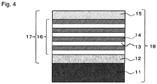
- FIG. 4 is a schematic diagram showing an example of the cross-sectional structure of the coated drill of the present embodiment, and the number of repeats will be described below by using this schematic diagram.
- a coated drill 18 includes a substrate 11 and a coating layer 17 formed on the surface of the substrate 11. The coating layer 17 is formed by laminating a lower layer 12, which will be described hereinbelow, an alternating laminate structure 16, and an upper layer 15, which will be described later, in order of description from the substrate 11 side.
- the alternating laminate structure 16 is formed by alternately laminating a first composite nitride layer 13 and a second composite nitride layer 14 in the order of description from the lower layer 12 side to the upper layer 15 side, the first composite nitride layer 13 and the second composite nitride layer 14 each being laminated four times. In this case, the number of repeats is four.
- the first composite nitride layer 13 and the second composite nitride layer 14 are sequentially formed from the lower layer 12 side to the upper layer 15 side in the order of the first composite nitride layer 13, the second composite nitride layer 14, the first composite nitride layer 13, the second composite nitride layer 14, the first composite nitride layer 13, the second composite nitride layer 14, the first composite nitride layer 13, the second composite nitride layer 14, the first composite nitride layer 13, the second composite nitride layer 14, the first composite nitride layer 13, and the second composite nitride layer 14, the number of repeats is five.
- the coating layer 17 includes both the lower layer 12 and the upper layer 15, but the coating layer may include only either the lower layer 12 or the upper layer 15, or none of these layers.
- the average thickness of the alternating laminate structure is 1.50 ⁇ m or more, the wear resistance is further improved, and where the average thickness is 12.00 ⁇ m or less, the chipping resistance is further improved. Therefore, the average thickness of the alternating laminate structure is preferably 1.50 ⁇ m or more and 12.00 ⁇ m or less. Within this range, from the same viewpoint as above, the average thickness is more preferably 3.00 ⁇ m or more and 9.00 ⁇ m or less.
- the chipping resistance is further improved.
- the wear resistance is further improved.
- the chipping resistance of the coated drill of the present embodiment is further improved mainly because the grains of the second composite nitride layer are refined when the FWHM for the (200) plane is 0.4° or more and that the wear resistance of the coated drill of the present embodiment is further improved mainly because lattice strains are small and excellent adhesiveness is realized when the FWHM for the (200) plane is 1.0° or less, but the present invention is not limited by these factors. Therefore, it is preferable that the FWHM for the (200) plane be 0.4° or more and 1.0° or less. Within this range, from the same viewpoint as above, the FWHM is more preferably 0.6° or more and 1.0° or less, and even more preferably 0.7° or more and 1.0° or less.
- the FWHM for the (200) plane in the X-ray diffraction of the second composite nitride layer can be measured, for example, under the following measurement conditions.
- Characteristic X ray CuK ⁇ ray, monochromator: Ni, divergence slit: 1/2°, scattering slit: 2/3°, receiving slit: 0.15 mm, and sampling width: 0.01°.
- the coating layer used in the present embodiment may be composed only of the alternating laminate structure of composite nitride layers, but it is preferable that the coating layer have a lower layer between the substrate and the alternating laminate structure (that is, the lower layer of the alternate laminates structure) because adhesiveness between the substrate and the alternating laminate structure is further improved.
- the lower layer preferably contains a compound including an element of at least one kind selected from the group consisting of Ti, Zr, Hf, V, Nb, Ta, Cr, Mo, W, Al, Si, and Y and an element of at least one kind selected from the group consisting of C, N, O and B, more preferably a compound including an element of at least one kind selected from the group consisting of Ti, V, Nb, Ta, Cr, Mo, W, Al, Si, and Y and an element of at least one kind selected from the group consisting of C, N, O and B, and even more preferably a compound including an element of at least one kind selected from the group consisting of Ti, Ta, Cr, W, Al, Si, and Y and N.
- the lower layer may be a single layer or a multilayer (laminated) structure including two or more layers.
- the average thickness of the lower layer be 0.1 ⁇ m or more and 3.5 ⁇ m or less because adhesiveness between the substrate and the coating layer tends to further improve.
- the average thickness of the lower layer is more preferably 0.2 ⁇ m or more and 3.0 ⁇ m or less, and further preferably 0.3 ⁇ m or more and 2.5 ⁇ m or less.
- the coating layer used in the present embodiment may have an upper layer on the side of the alternating laminate structure opposite that facing the substrate (that is, the upper layer of the alternating laminate structure), preferably on the surface of the alternating laminate structure. It is further preferable that the upper layer contains a compound including an element of at least one kind selected from the group consisting of Ti, Zr, Hf, V, Nb, Ta, Cr, Mo, W, Al, Si, and Y and an element of at least one kind selected from the group consisting of C, N, O and B because wear resistance is further improved.
- the upper layer preferably contains a compound including an element of at least one kind selected from the group consisting of Ti, Zr, Hf, V, Nb, Ta, Cr, Mo, W, Al, Si, and Y and an element of at least one kind selected from the group consisting of C, N, O and B, more preferably a compound including an element of at least one kind selected from the group consisting of Ti, V, Nb, Ta, Cr, Mo, W, Al, Si, and Y and an element of at least one kind selected from the group consisting of C, N, O and B, and even more preferably a compound including an element of at least one kind selected from the group consisting of Ti, Nb, Ta, Cr, W, Al, Si, and Y and N.
- the upper layer may be a single layer or a multilayer (laminated) structure including two or more layers.
- the average thickness of the upper layer be 0.1 ⁇ m or more and 3.5 ⁇ m or less because wear resistance tends to improve. From the same viewpoint, the average thickness of the upper layer is more preferably 0.2 ⁇ m or more and 3.0 ⁇ m or less, and further preferably 0.3 ⁇ m or more and 2.5 ⁇ m or less.
- a method of manufacturing the coating layer used for the coated drill of the present embodiment is not particularly limited, and for example, physical vapor deposition methods such as an ion plating method, an arc ion plating method, a sputtering method, an ion mixing method, and the like can be used. It is preferable that the coating layer be formed using a physical vapor deposition method because a sharp edge can be formed. Among the physical vapor deposition method, the arc ion plating method is more preferable because excellent adhesiveness between the coating layer and the substrate is attained.
- the method of manufacturing the coated drill of the present embodiment will be described below with reference to specific examples.
- the method of manufacturing the coated drill of the present embodiment is not particularly limited as long as the configuration of the coated drill can be achieved.
- a substrate processed into a tool shape is received in a reactor of a physical vapor deposition apparatus, and a metal evaporation source is set in the reactor. Thereafter, the interior of the reactor is evacuated until the pressure becomes 1.0 ⁇ 10 -2 Pa or less, and the substrate is heated with a heater in the reactor until the substrate temperature reaches 200°C to 700°C. After heating, Ar gas is introduced into the reactor to set the pressure inside the reactor to 0.5 Pa to 5.0 Pa.
- a bias voltage of -500 V to -350 V is applied to the substrate in the Ar gas atmosphere at a pressure of 0.5 Pa to 5.0 Pa and an electric current of 40 A to 50 A is passed through the tungsten filament in the reactor so that the surface of the substrate is subjected to ion bombardment treatment with Ar gas.
- the interior of the reactor is evacuated until the pressure reaches a vacuum of 1.0 ⁇ 10 -2 Pa or less.
- the substrate is heated until its temperature reaches 400°C to 600°C. After heating, a gas is introduced into the reactor, and the pressure inside the reactor is set to 0.5 Pa to 5.0 Pa.
- the gas is exemplified by N 2
- the lower layer is configured of a compound including an element of at least one kind selected from the group consisting of Ti, Zr, Hf, V, Nb, Ta, Cr, Mo, W, Al, Si, and Y and also N and C
- the gas is exemplified by a mixed gas of N 2 and C 2 H 2 .
- the substrate is controlled so that the temperature reaches 400°C to 600°C, a gas is introduced into the reactor, and the pressure inside the reactor is set to 0.5 Pa to 5.0 Pa.
- the gas is exemplified by a mixed gas of Ar gas and N 2 gas.
- a bias voltage of -80 V to -40 V may be applied to the substrate, and a metal evaporation source corresponding to the metal component of the first composite nitride layer is evaporated by arc discharge with an arc current of 100 A to 200 A to form the first composite nitride layer.
- the C Cr may be increased.
- the pressure in the above reactor may be decreased or the volume ratio of the Ar gas in the mixed gas may be increased.
- the C Cr can be increased by forming the first composite nitride layer in a state in which a portion of the substrate corresponding to the margin portion of the coated drill is disposed to face the metal evaporation source. In this case, the C Cr increases and the M Cr decreases.
- the substrate is controlled so that the temperature thereof reaches 400°C to 600°C. It is preferable that the temperature of the substrate be made equal to the temperature of the substrate when the first composite nitride layer is formed because the first composite nitride layer and the second composite nitride layer can be formed continuously.
- a mixed gas same as that used when the first composite nitride layer is formed is introduced into the reactor, and the pressure inside the reactor is set to 0.5 Pa to 5.0 Pa.
- a bias voltage of -80 V to -40 V may be applied to the substrate, and a metal evaporation source corresponding to the metal component of the second composite nitride layer is evaporated by arc discharge with an arc current of 100 A to 200 A to form the second composite nitride layer.
- two or more kinds of metal evaporation sources may be alternately evaporated by arc discharge under the above-mentioned conditions, thereby alternately forming respective composite nitride layers.
- the thickness of each composite nitride layer constituting the alternate laminate structure can be controlled.
- the film formation temperature or adjust the bias voltage, or adjust the lamination interval when the alternating laminate structure is formed. More specifically, when a lower film formation temperature is set, a higher negative bias voltage is applied, or the lamination interval is increased, the value of the FWHM for the (200) plane increases.
- the upper layer may be formed under the same manufacturing conditions as the above-mentioned lower layer. That is, first, the substrate is heated until its temperature reaches 400°C to 600°C. After heating, a gas is introduced into the reactor, and the pressure inside the reactor is set to 0.5 Pa to 5.0 Pa.
- the gas is exemplified by N 2
- the gas is exemplified by a mixed gas of N 2 and C 2 H 2 .
- a bias voltage of -80 V to -40 V may be applied to the substrate, and a metal evaporation source corresponding to the metal component of each layer is evaporated by arc discharge with an arc current of 100 A to 200 A to form the lower layer.
- the thickness of each layer constituting the coating layer in the coated drill of the present embodiment can be measured from the cross-sectional structure of the coated drill by using an optical microscope, a scanning electron microscope (SEM), a transmission electron microscope (TEM), or the like.
- the average thickness of each layer in the coated drill of the present embodiment can be obtained by measuring the thickness of each layer from the cross sections at three or more locations in the chisel edge portion and calculating the average value (arithmetic average value) thereof.
- composition of each layer constituting the coating layer in the coated drill of the present embodiment can be also determined from the cross-sectional structure of the coated drill of the present embodiment by using an energy dispersive X-ray analyzer (EDS) or a wavelength dispersive X-ray analyzer (WDS).
- EDS energy dispersive X-ray analyzer
- WDS wavelength dispersive X-ray analyzer
- a cemented carbide having a composition of 89.6% WC - 9.8% Co - 0.6% Cr 3 C 2 (% by mass hereinabove) was prepared as a substrate by processing into an insert shape of DMP120 (made by Tungaloy Corporation).
- Metal evaporation sources corresponding to the composition of each layer shown in Tables 1 and 2 were arranged in the reactor of the arc ion plating apparatus so as to face the portion of the substrate corresponding to the margin portion when forming the coated drill of invention samples 1 to 32 and comparative samples 1, 2, 5 to 7, and 9 to 11.
- metal evaporation sources corresponding to the composition of each layer shown in Tables 1 and 2 were arranged in the reactor of the arc ion plating apparatus so as to face the portion of the substrate corresponding to the chisel edge portion.
- the prepared substrate was fixed to the fixing bracket of the rotary table in the reactor.
- the inside of the reactor was evacuated until the pressure reached a vacuum of 5.0 ⁇ 10 -3 Pa or less.
- the substrate was heated with a heater in the reactor to a temperature of 450°C. After heating, Ar gas was introduced into the reactor such that the pressure became 2.7 Pa.
- a bias voltage of -400 V was applied to the substrate in the Ar gas atmosphere at a pressure of 2.7 Pa and an electric current of 40 A was passed through the tungsten filament in the reactor so that the surface of the substrate was subjected to ion bombardment treatment with Ar gas. The treatment was performed for 30 min. After completing the ion bombardment treatment, the interior of the reactor was evacuated until the pressure reached a vacuum of 5.0 ⁇ 10 -3 Pa or less.
- the bias voltage shown in Table 3 was applied to the substrate, and the metal evaporation sources of the first composite nitride layer and the second composite nitride layer having the compositions shown in Table 1 were alternately evaporated by an arc discharge of a current (arc current) shown in Table 3 to form the first composite nitride layer and the second composite nitride layer alternately on the surface of the substrate.
- a current arc current
- the gas condition and the pressure in the reactor were controlled to become such as shown in Table 3.
- the thickness of the first composite nitride layer and the thickness of the second composite nitride layer were controlled by adjusting the respective arc discharge time so as to obtain the thickness values shown in Table 1.
- the substrate was controlled so that the temperature thereof reached the film formation temperature (temperature at the start of film formation) shown in Table 4, argon gas (Ar) and nitrogen gas (N 2 ) were introduced into the reactor at the volume ratio shown in Table 4, and the gas conditions were adjusted so that the inside of the reactor had the pressure shown in Table 4. Thereafter, the bias voltage shown in Table 4 was applied to the substrate, and the metal evaporation source having the composition shown in Table 2 was evaporated by an arc discharge of an arc current shown in Table 4 to form a single layer (layer A or layer B) having the thickness shown in Table 2 on the surface of the substrate.
- argon gas (Ar) and nitrogen gas (N 2 ) were introduced into the reactor at the volume ratio shown in Table 4, and the gas conditions were adjusted so that the inside of the reactor had the pressure shown in Table 4.
- the bias voltage shown in Table 4 was applied to the substrate, and the metal evaporation source having the composition shown in Table 2 was evaporated by an arc discharge of an arc current shown in Table 4 to form a
- the substrate was controlled so that the temperature thereof reached the film formation temperature (temperature at the start of film formation) shown in Table 4, argon gas (Ar) and nitrogen gas (N 2 ) were introduced into the reactor at the volume ratio shown in Table 4, and the gas conditions were adjusted so that the inside of the reactor had the pressure shown in Table 4.
- the bias voltage shown in Table 4 was applied to the substrate, and the metal evaporation sources of the layer A and the layer B having the compositions shown in Table 2 were alternately evaporated by an arc discharge of a current (arc current) shown in Table 4 to form the layer A and the layer B alternately on the surface of the substrate.
- the gas condition and the pressure in the reactor were controlled to become such as shown in Table 4.
- the thickness of the layer A and the layer B were controlled by adjusting the respective arc discharge time so as to obtain the thickness values shown in Table 2.
- the average thickness of each layer of the obtained sample was determined by performing TEM observation of three cross sections at the chisel edge portion of the coated drill, measuring the thickness of each layer, and calculating the average value (arithmetic average value) thereof. The results are also shown in Tables 1 and 2.
- composition of each layer of the obtained sample was measured at the chisel edge portion of the coated drill by using the EDS attached to the TEM. The results are also shown in Tables 1 and 2.
- the composition ratio of the metal elements in each layer in Tables 1 and 2 indicates the atomic ratio of each metal element based on the total of metal elements in the metal compound constituting each layer.
- the composition of the second composite nitride layer in the margin portion of the obtained sample was the same as the composition of the second composite nitride layer in the chisel edge portion shown in Table 1.
- the obtained samples were evaluated by performing the following cutting test.
- Workpiece S55C (200 HB)
- Workpiece shape rectangular parallelepiped block of 150 mm ⁇ 200 mm ⁇ 40 mm
- Machining form blind hole
- Cutting speed 110 m/min
- Feed rate per one revolution 0.27 mm/rev
- Coolant water-soluble (internal lubrication method)
- a cemented carbide having a composition of 89.6% WC - 9.8% Co - 0.6% Cr 3 C 2 (% by mass hereinabove) was prepared as a substrate by machining into an insert shape of DMP120 (made by Tungaloy Corporation).
- Metal evaporation sources corresponding to the composition of each layer shown in Table 11 were arranged in the reactor of the arc ion plating apparatus so as to face the portion of the substrate corresponding to the margin portion when forming the coated drill.
- the prepared substrate was fixed to the fixing bracket of the rotary table in the reactor.
- the inside of the reactor was evacuated until the pressure reached a vacuum of 5.0 ⁇ 10 -3 Pa or less.
- the substrate was heated with a heater in the reactor to a temperature of 450°C. After heating, Ar gas was introduced into the reactor such that the pressure became 2.7 Pa.
- a bias voltage of -400 V was applied to the substrate in the Ar gas atmosphere at a pressure of 2.7 Pa and an electric current of 40 A was passed through the tungsten filament in the reactor so that the surface of the substrate was subjected to ion bombardment treatment with Ar gas. The treatment was performed for 30 min. After completing the ion bombardment treatment, the interior of the reactor was evacuated until the pressure reached a vacuum of 5.0 ⁇ 10 -3 Pa or less.
- the first composite nitride layer and the second composite nitride layer were alternately formed on the lower layer or the surface of the substrate to obtain invention samples 33 to 35 under the same manufacturing conditions as those of the alternating laminate structure of invention sample 1, to obtain invention samples 36 to 38 under the same manufacturing conditions as those of the alternating laminate structure of invention sample 11, to obtain invention samples 39 to 42 under the same manufacturing conditions as those of the alternating laminate structure of invention sample 23, and to obtain invention samples 43 to 46 under the same manufacturing conditions as those of the alternating laminate structure of invention sample 25.
- sample numbers described in the alternating laminate structure of invention samples 33 to 46 in Table 11 indicate that the alternating laminate structure of each of invention samples 33 to 46 and the alternating laminate structure of the corresponding sample numbers are the same.
- the alternating laminate structure of invention sample 33 is the same as the alternating laminate structure of invention sample 1.
- the average thickness of each layer of the obtained sample was obtained by performing TEM observation of three cross sections at the chisel edge portion of the coated drill, measuring the thickness of each layer, and calculating the average value (arithmetic average value) thereof. The results are also shown in Table 11.
- compositions of the lower layer and the upper layer of the obtained sample were measured at the chisel edge portion of the coated drill by using the EDS attached to the TEM. The results are also shown in Table 11.
- the composition ratio of the metal elements in each layer in Table 11 indicates the atomic ratio of each metal element based on the total of metal elements in the metal compound constituting each layer.
- the obtained samples were used to perform the cutting test and evaluation in the same manner as in Example 1.
- the machining length up to the tool life in the cutting test was rated "A” at 100 m or more, “B” at 60 m or more and less than 100 m, and "C” at less than 60 m.
- "A” is the best
- "B” is the second best
- "C” is the worst, which means that the more evaluations of "A” or "B” are, the better the cutting performance is.
- a large machining length means excellent chipping resistance and wear resistance.
- Table 13 Sample No.
- the invention samples have excellent wear resistance and chipping resistance even when the invention samples have an upper layer and/or a lower layer, and the tool life is extended.
- the coated drill of the present invention is excellent in wear resistance and chipping resistance, so that tool life can be extended as compared with the conventional one. Therefore, the coated drill has high industrial applicability.
Landscapes
- Chemical & Material Sciences (AREA)
- Engineering & Computer Science (AREA)
- Mechanical Engineering (AREA)
- Chemical Kinetics & Catalysis (AREA)
- Materials Engineering (AREA)
- Metallurgy (AREA)
- Organic Chemistry (AREA)
- Inorganic Chemistry (AREA)
- General Chemical & Material Sciences (AREA)
- Drilling Tools (AREA)
- Physical Vapour Deposition (AREA)
- Cutting Tools, Boring Holders, And Turrets (AREA)
Applications Claiming Priority (1)
| Application Number | Priority Date | Filing Date | Title |
|---|---|---|---|
| JP2017179177A JP6642836B2 (ja) | 2017-09-19 | 2017-09-19 | 被覆ドリル |
Publications (2)
| Publication Number | Publication Date |
|---|---|
| EP3456867A1 true EP3456867A1 (fr) | 2019-03-20 |
| EP3456867B1 EP3456867B1 (fr) | 2020-11-04 |
Family
ID=63642649
Family Applications (1)
| Application Number | Title | Priority Date | Filing Date |
|---|---|---|---|
| EP18195076.7A Active EP3456867B1 (fr) | 2017-09-19 | 2018-09-18 | Foret revêtu |
Country Status (4)
| Country | Link |
|---|---|
| US (1) | US10583494B2 (fr) |
| EP (1) | EP3456867B1 (fr) |
| JP (1) | JP6642836B2 (fr) |
| CN (1) | CN109513972B (fr) |
Cited By (1)
| Publication number | Priority date | Publication date | Assignee | Title |
|---|---|---|---|---|
| CN113134393A (zh) * | 2021-04-09 | 2021-07-20 | 南通大学 | 一种光催化双氯芬酸净化膜及其制备方法 |
Families Citing this family (4)
| Publication number | Priority date | Publication date | Assignee | Title |
|---|---|---|---|---|
| JP7464360B2 (ja) * | 2019-07-04 | 2024-04-09 | 住友化学株式会社 | 圧電積層体、圧電素子および圧電積層体の製造方法 |
| CN110863173B (zh) * | 2019-10-29 | 2022-08-12 | 富联科技(山西)有限公司 | Pvd膜层及其制备方法及具有该膜层的金属制品 |
| WO2022112605A1 (fr) * | 2020-11-30 | 2022-06-02 | Oerlikon Surface Solutions Ag, Pfäffikon | Revêtement multicouche à base de nitrure de molybdène pour réduction de l'usure et du frottement |
| JPWO2024185311A1 (fr) * | 2023-03-06 | 2024-09-12 |
Citations (2)
| Publication number | Priority date | Publication date | Assignee | Title |
|---|---|---|---|---|
| JP2008188689A (ja) * | 2007-02-01 | 2008-08-21 | Sumitomo Electric Hardmetal Corp | 表面被覆切削工具 |
| US20150232978A1 (en) * | 2012-09-28 | 2015-08-20 | Walter Ag | Tool with TiAlCrSiN PVD coating |
Family Cites Families (13)
| Publication number | Priority date | Publication date | Assignee | Title |
|---|---|---|---|---|
| DE3825399C5 (de) * | 1988-07-23 | 2005-05-12 | Cemecon Ag | PVD- oder Plasma- CVD-Beschichtung |
| JP2538864Y2 (ja) * | 1991-09-26 | 1997-06-18 | オーエスジー株式会社 | 難削材用硬質膜被覆ドリル |
| EP1992717B1 (fr) * | 2000-12-28 | 2012-02-15 | Kabushiki Kaisha Kobe Seiko Sho | Utilisation d'un' cible pour la placage ionique à l'arc pour former un film rigide |
| JP3931328B2 (ja) * | 2001-11-15 | 2007-06-13 | 三菱マテリアル株式会社 | 高速切削加工で硬質被覆層がすぐれた耐摩耗性を発揮する表面被覆超硬合金製切削工具 |
| US7348074B2 (en) * | 2005-04-01 | 2008-03-25 | Oc Oerlikon Balzers Ag | Multilayer hard coating for tools |
| WO2010150335A1 (fr) * | 2009-06-22 | 2010-12-29 | 株式会社タンガロイ | Outil comportant un corps fritté en nitrure de bore cubique revêtu |
| JP2011177825A (ja) * | 2010-03-01 | 2011-09-15 | Mitsubishi Materials Corp | 表面被覆超硬合金製ドリル |
| US8673435B2 (en) * | 2010-07-06 | 2014-03-18 | Tungaloy Corporation | Coated cBN sintered body tool |
| JP5892331B2 (ja) * | 2011-07-22 | 2016-03-23 | 三菱マテリアル株式会社 | 潤滑特性と耐摩耗性にすぐれた表面被覆ドリル |
| EP2965842B1 (fr) * | 2013-03-04 | 2018-12-12 | Tungaloy Corporation | Outil de coupe garni d'un revêtement |
| US10189089B2 (en) * | 2014-07-25 | 2019-01-29 | Tungaloy Corporation | Coated cutting tool |
| JP6390706B2 (ja) * | 2014-08-01 | 2018-09-19 | 株式会社タンガロイ | 被覆切削工具 |
| JP6858347B2 (ja) * | 2017-07-28 | 2021-04-14 | 株式会社タンガロイ | 被覆切削工具 |
-
2017
- 2017-09-19 JP JP2017179177A patent/JP6642836B2/ja active Active
-
2018
- 2018-09-05 CN CN201811033200.1A patent/CN109513972B/zh active Active
- 2018-09-14 US US16/131,129 patent/US10583494B2/en active Active
- 2018-09-18 EP EP18195076.7A patent/EP3456867B1/fr active Active
Patent Citations (3)
| Publication number | Priority date | Publication date | Assignee | Title |
|---|---|---|---|---|
| JP2008188689A (ja) * | 2007-02-01 | 2008-08-21 | Sumitomo Electric Hardmetal Corp | 表面被覆切削工具 |
| US20150232978A1 (en) * | 2012-09-28 | 2015-08-20 | Walter Ag | Tool with TiAlCrSiN PVD coating |
| JP2015530270A (ja) | 2012-09-28 | 2015-10-15 | バルター アクチェンゲゼルシャフト | PVDによるTiAlCrSiN被膜を有する工具 |
Cited By (2)
| Publication number | Priority date | Publication date | Assignee | Title |
|---|---|---|---|---|
| CN113134393A (zh) * | 2021-04-09 | 2021-07-20 | 南通大学 | 一种光催化双氯芬酸净化膜及其制备方法 |
| CN113134393B (zh) * | 2021-04-09 | 2023-04-25 | 南通大学 | 一种光催化双氯芬酸净化膜及其制备方法 |
Also Published As
| Publication number | Publication date |
|---|---|
| US10583494B2 (en) | 2020-03-10 |
| JP2019051581A (ja) | 2019-04-04 |
| EP3456867B1 (fr) | 2020-11-04 |
| CN109513972A (zh) | 2019-03-26 |
| US20190084052A1 (en) | 2019-03-21 |
| CN109513972B (zh) | 2020-07-17 |
| JP6642836B2 (ja) | 2020-02-12 |
Similar Documents
| Publication | Publication Date | Title |
|---|---|---|
| JP5817932B2 (ja) | 被覆工具 | |
| EP3290137B1 (fr) | Outil de coupe revêtu | |
| EP3225337B1 (fr) | Outil de coupe à revêtement de surface présentant une excellente résistance à l'écaillage et une excellente résistance à l'usure | |
| EP3173169B1 (fr) | Outil de coupe revêtu | |
| EP3434809A1 (fr) | Outil de coupe recouvert | |
| US20190040519A1 (en) | Surface-coated cutting tool providing excellent chipping resistance and wear resistance in heavy intermittent cutting | |
| EP3130418A1 (fr) | Outil revêtu | |
| EP3456867B1 (fr) | Foret revêtu | |
| EP3360631A1 (fr) | Outil de coupe revêtu | |
| EP2623241A1 (fr) | Outil de coupe | |
| US9725811B2 (en) | Coated cutting tool | |
| EP3124146A1 (fr) | Outil revêtu | |
| EP3332899B1 (fr) | Outil de coupe revêtu | |
| EP3360632B1 (fr) | Outil de coupe revêtu | |
| EP3395484B1 (fr) | Outil compact fritté en nitrure de bore cubique à surface revêtue | |
| EP3275577B1 (fr) | Outil de coupe revêtu | |
| WO2016148056A1 (fr) | Outil de coupe à revêtement de surface, doté de couches de revêtement rigides présentant une excellente résistance à l'écaillage | |
| JP2019005894A (ja) | 被覆切削工具 | |
| US11982000B2 (en) | Coated cutting tool | |
| JP7108966B2 (ja) | 被覆切削工具 | |
| EP4253600A1 (fr) | Outil de coupe revêtu | |
| JP2017024136A (ja) | 被覆切削工具 |
Legal Events
| Date | Code | Title | Description |
|---|---|---|---|
| PUAI | Public reference made under article 153(3) epc to a published international application that has entered the european phase |
Free format text: ORIGINAL CODE: 0009012 |
|
| STAA | Information on the status of an ep patent application or granted ep patent |
Free format text: STATUS: REQUEST FOR EXAMINATION WAS MADE |
|
| 17P | Request for examination filed |
Effective date: 20180918 |
|
| AK | Designated contracting states |
Kind code of ref document: A1 Designated state(s): AL AT BE BG CH CY CZ DE DK EE ES FI FR GB GR HR HU IE IS IT LI LT LU LV MC MK MT NL NO PL PT RO RS SE SI SK SM TR |
|
| AX | Request for extension of the european patent |
Extension state: BA ME |
|
| RIC1 | Information provided on ipc code assigned before grant |
Ipc: C23C 16/32 20060101ALI20191205BHEP Ipc: C23C 14/02 20060101ALI20191205BHEP Ipc: C23C 30/00 20060101ALI20191205BHEP Ipc: C23C 28/04 20060101AFI20191205BHEP Ipc: C23C 14/06 20060101ALI20191205BHEP Ipc: C23C 28/00 20060101ALI20191205BHEP |
|
| GRAP | Despatch of communication of intention to grant a patent |
Free format text: ORIGINAL CODE: EPIDOSNIGR1 |
|
| STAA | Information on the status of an ep patent application or granted ep patent |
Free format text: STATUS: GRANT OF PATENT IS INTENDED |
|
| INTG | Intention to grant announced |
Effective date: 20200114 |
|
| GRAS | Grant fee paid |
Free format text: ORIGINAL CODE: EPIDOSNIGR3 |
|
| GRAJ | Information related to disapproval of communication of intention to grant by the applicant or resumption of examination proceedings by the epo deleted |
Free format text: ORIGINAL CODE: EPIDOSDIGR1 |
|
| GRAL | Information related to payment of fee for publishing/printing deleted |
Free format text: ORIGINAL CODE: EPIDOSDIGR3 |
|
| STAA | Information on the status of an ep patent application or granted ep patent |
Free format text: STATUS: REQUEST FOR EXAMINATION WAS MADE |
|
| GRAP | Despatch of communication of intention to grant a patent |
Free format text: ORIGINAL CODE: EPIDOSNIGR1 |
|
| STAA | Information on the status of an ep patent application or granted ep patent |
Free format text: STATUS: GRANT OF PATENT IS INTENDED |
|
| INTC | Intention to grant announced (deleted) | ||
| INTG | Intention to grant announced |
Effective date: 20200609 |
|
| GRAA | (expected) grant |
Free format text: ORIGINAL CODE: 0009210 |
|
| STAA | Information on the status of an ep patent application or granted ep patent |
Free format text: STATUS: THE PATENT HAS BEEN GRANTED |
|
| AK | Designated contracting states |
Kind code of ref document: B1 Designated state(s): AL AT BE BG CH CY CZ DE DK EE ES FI FR GB GR HR HU IE IS IT LI LT LU LV MC MK MT NL NO PL PT RO RS SE SI SK SM TR |
|
| REG | Reference to a national code |
Ref country code: GB Ref legal event code: FG4D |
|
| REG | Reference to a national code |
Ref country code: CH Ref legal event code: EP |
|
| REG | Reference to a national code |
Ref country code: AT Ref legal event code: REF Ref document number: 1330939 Country of ref document: AT Kind code of ref document: T Effective date: 20201115 |
|
| REG | Reference to a national code |
Ref country code: IE Ref legal event code: FG4D |
|
| REG | Reference to a national code |
Ref country code: DE Ref legal event code: R096 Ref document number: 602018009376 Country of ref document: DE |
|
| REG | Reference to a national code |
Ref country code: NL Ref legal event code: MP Effective date: 20201104 |
|
| REG | Reference to a national code |
Ref country code: AT Ref legal event code: MK05 Ref document number: 1330939 Country of ref document: AT Kind code of ref document: T Effective date: 20201104 |
|
| PG25 | Lapsed in a contracting state [announced via postgrant information from national office to epo] |
Ref country code: FI Free format text: LAPSE BECAUSE OF FAILURE TO SUBMIT A TRANSLATION OF THE DESCRIPTION OR TO PAY THE FEE WITHIN THE PRESCRIBED TIME-LIMIT Effective date: 20201104 Ref country code: RS Free format text: LAPSE BECAUSE OF FAILURE TO SUBMIT A TRANSLATION OF THE DESCRIPTION OR TO PAY THE FEE WITHIN THE PRESCRIBED TIME-LIMIT Effective date: 20201104 Ref country code: PT Free format text: LAPSE BECAUSE OF FAILURE TO SUBMIT A TRANSLATION OF THE DESCRIPTION OR TO PAY THE FEE WITHIN THE PRESCRIBED TIME-LIMIT Effective date: 20210304 Ref country code: GR Free format text: LAPSE BECAUSE OF FAILURE TO SUBMIT A TRANSLATION OF THE DESCRIPTION OR TO PAY THE FEE WITHIN THE PRESCRIBED TIME-LIMIT Effective date: 20210205 Ref country code: NO Free format text: LAPSE BECAUSE OF FAILURE TO SUBMIT A TRANSLATION OF THE DESCRIPTION OR TO PAY THE FEE WITHIN THE PRESCRIBED TIME-LIMIT Effective date: 20210204 |
|
| PG25 | Lapsed in a contracting state [announced via postgrant information from national office to epo] |
Ref country code: BG Free format text: LAPSE BECAUSE OF FAILURE TO SUBMIT A TRANSLATION OF THE DESCRIPTION OR TO PAY THE FEE WITHIN THE PRESCRIBED TIME-LIMIT Effective date: 20210204 Ref country code: PL Free format text: LAPSE BECAUSE OF FAILURE TO SUBMIT A TRANSLATION OF THE DESCRIPTION OR TO PAY THE FEE WITHIN THE PRESCRIBED TIME-LIMIT Effective date: 20201104 Ref country code: LV Free format text: LAPSE BECAUSE OF FAILURE TO SUBMIT A TRANSLATION OF THE DESCRIPTION OR TO PAY THE FEE WITHIN THE PRESCRIBED TIME-LIMIT Effective date: 20201104 Ref country code: IS Free format text: LAPSE BECAUSE OF FAILURE TO SUBMIT A TRANSLATION OF THE DESCRIPTION OR TO PAY THE FEE WITHIN THE PRESCRIBED TIME-LIMIT Effective date: 20210304 Ref country code: SE Free format text: LAPSE BECAUSE OF FAILURE TO SUBMIT A TRANSLATION OF THE DESCRIPTION OR TO PAY THE FEE WITHIN THE PRESCRIBED TIME-LIMIT Effective date: 20201104 Ref country code: ES Free format text: LAPSE BECAUSE OF FAILURE TO SUBMIT A TRANSLATION OF THE DESCRIPTION OR TO PAY THE FEE WITHIN THE PRESCRIBED TIME-LIMIT Effective date: 20201104 Ref country code: AT Free format text: LAPSE BECAUSE OF FAILURE TO SUBMIT A TRANSLATION OF THE DESCRIPTION OR TO PAY THE FEE WITHIN THE PRESCRIBED TIME-LIMIT Effective date: 20201104 |
|
| REG | Reference to a national code |
Ref country code: LT Ref legal event code: MG9D |
|
| PG25 | Lapsed in a contracting state [announced via postgrant information from national office to epo] |
Ref country code: HR Free format text: LAPSE BECAUSE OF FAILURE TO SUBMIT A TRANSLATION OF THE DESCRIPTION OR TO PAY THE FEE WITHIN THE PRESCRIBED TIME-LIMIT Effective date: 20201104 |
|
| PG25 | Lapsed in a contracting state [announced via postgrant information from national office to epo] |
Ref country code: SM Free format text: LAPSE BECAUSE OF FAILURE TO SUBMIT A TRANSLATION OF THE DESCRIPTION OR TO PAY THE FEE WITHIN THE PRESCRIBED TIME-LIMIT Effective date: 20201104 Ref country code: CZ Free format text: LAPSE BECAUSE OF FAILURE TO SUBMIT A TRANSLATION OF THE DESCRIPTION OR TO PAY THE FEE WITHIN THE PRESCRIBED TIME-LIMIT Effective date: 20201104 Ref country code: EE Free format text: LAPSE BECAUSE OF FAILURE TO SUBMIT A TRANSLATION OF THE DESCRIPTION OR TO PAY THE FEE WITHIN THE PRESCRIBED TIME-LIMIT Effective date: 20201104 Ref country code: RO Free format text: LAPSE BECAUSE OF FAILURE TO SUBMIT A TRANSLATION OF THE DESCRIPTION OR TO PAY THE FEE WITHIN THE PRESCRIBED TIME-LIMIT Effective date: 20201104 Ref country code: SK Free format text: LAPSE BECAUSE OF FAILURE TO SUBMIT A TRANSLATION OF THE DESCRIPTION OR TO PAY THE FEE WITHIN THE PRESCRIBED TIME-LIMIT Effective date: 20201104 Ref country code: LT Free format text: LAPSE BECAUSE OF FAILURE TO SUBMIT A TRANSLATION OF THE DESCRIPTION OR TO PAY THE FEE WITHIN THE PRESCRIBED TIME-LIMIT Effective date: 20201104 |
|
| REG | Reference to a national code |
Ref country code: DE Ref legal event code: R097 Ref document number: 602018009376 Country of ref document: DE |
|
| PG25 | Lapsed in a contracting state [announced via postgrant information from national office to epo] |
Ref country code: DK Free format text: LAPSE BECAUSE OF FAILURE TO SUBMIT A TRANSLATION OF THE DESCRIPTION OR TO PAY THE FEE WITHIN THE PRESCRIBED TIME-LIMIT Effective date: 20201104 |
|
| PLBE | No opposition filed within time limit |
Free format text: ORIGINAL CODE: 0009261 |
|
| STAA | Information on the status of an ep patent application or granted ep patent |
Free format text: STATUS: NO OPPOSITION FILED WITHIN TIME LIMIT |
|
| 26N | No opposition filed |
Effective date: 20210805 |
|
| PG25 | Lapsed in a contracting state [announced via postgrant information from national office to epo] |
Ref country code: AL Free format text: LAPSE BECAUSE OF FAILURE TO SUBMIT A TRANSLATION OF THE DESCRIPTION OR TO PAY THE FEE WITHIN THE PRESCRIBED TIME-LIMIT Effective date: 20201104 Ref country code: NL Free format text: LAPSE BECAUSE OF FAILURE TO SUBMIT A TRANSLATION OF THE DESCRIPTION OR TO PAY THE FEE WITHIN THE PRESCRIBED TIME-LIMIT Effective date: 20201104 |
|
| PG25 | Lapsed in a contracting state [announced via postgrant information from national office to epo] |
Ref country code: SI Free format text: LAPSE BECAUSE OF FAILURE TO SUBMIT A TRANSLATION OF THE DESCRIPTION OR TO PAY THE FEE WITHIN THE PRESCRIBED TIME-LIMIT Effective date: 20201104 |
|
| REG | Reference to a national code |
Ref country code: CH Ref legal event code: PL |
|
| REG | Reference to a national code |
Ref country code: BE Ref legal event code: MM Effective date: 20210930 |
|
| PG25 | Lapsed in a contracting state [announced via postgrant information from national office to epo] |
Ref country code: IS Free format text: LAPSE BECAUSE OF FAILURE TO SUBMIT A TRANSLATION OF THE DESCRIPTION OR TO PAY THE FEE WITHIN THE PRESCRIBED TIME-LIMIT Effective date: 20210304 Ref country code: MC Free format text: LAPSE BECAUSE OF FAILURE TO SUBMIT A TRANSLATION OF THE DESCRIPTION OR TO PAY THE FEE WITHIN THE PRESCRIBED TIME-LIMIT Effective date: 20201104 |
|
| PG25 | Lapsed in a contracting state [announced via postgrant information from national office to epo] |
Ref country code: LU Free format text: LAPSE BECAUSE OF NON-PAYMENT OF DUE FEES Effective date: 20210918 Ref country code: IE Free format text: LAPSE BECAUSE OF NON-PAYMENT OF DUE FEES Effective date: 20210918 Ref country code: FR Free format text: LAPSE BECAUSE OF NON-PAYMENT OF DUE FEES Effective date: 20210930 Ref country code: BE Free format text: LAPSE BECAUSE OF NON-PAYMENT OF DUE FEES Effective date: 20210930 |
|
| PG25 | Lapsed in a contracting state [announced via postgrant information from national office to epo] |
Ref country code: LI Free format text: LAPSE BECAUSE OF NON-PAYMENT OF DUE FEES Effective date: 20210930 Ref country code: CH Free format text: LAPSE BECAUSE OF NON-PAYMENT OF DUE FEES Effective date: 20210930 |
|
| GBPC | Gb: european patent ceased through non-payment of renewal fee |
Effective date: 20220918 |
|
| PG25 | Lapsed in a contracting state [announced via postgrant information from national office to epo] |
Ref country code: CY Free format text: LAPSE BECAUSE OF FAILURE TO SUBMIT A TRANSLATION OF THE DESCRIPTION OR TO PAY THE FEE WITHIN THE PRESCRIBED TIME-LIMIT Effective date: 20201104 |
|
| PG25 | Lapsed in a contracting state [announced via postgrant information from national office to epo] |
Ref country code: HU Free format text: LAPSE BECAUSE OF FAILURE TO SUBMIT A TRANSLATION OF THE DESCRIPTION OR TO PAY THE FEE WITHIN THE PRESCRIBED TIME-LIMIT; INVALID AB INITIO Effective date: 20180918 |
|
| PG25 | Lapsed in a contracting state [announced via postgrant information from national office to epo] |
Ref country code: GB Free format text: LAPSE BECAUSE OF NON-PAYMENT OF DUE FEES Effective date: 20220918 |
|
| PG25 | Lapsed in a contracting state [announced via postgrant information from national office to epo] |
Ref country code: MK Free format text: LAPSE BECAUSE OF FAILURE TO SUBMIT A TRANSLATION OF THE DESCRIPTION OR TO PAY THE FEE WITHIN THE PRESCRIBED TIME-LIMIT Effective date: 20201104 |
|
| PG25 | Lapsed in a contracting state [announced via postgrant information from national office to epo] |
Ref country code: TR Free format text: LAPSE BECAUSE OF FAILURE TO SUBMIT A TRANSLATION OF THE DESCRIPTION OR TO PAY THE FEE WITHIN THE PRESCRIBED TIME-LIMIT Effective date: 20201104 |
|
| PG25 | Lapsed in a contracting state [announced via postgrant information from national office to epo] |
Ref country code: MT Free format text: LAPSE BECAUSE OF FAILURE TO SUBMIT A TRANSLATION OF THE DESCRIPTION OR TO PAY THE FEE WITHIN THE PRESCRIBED TIME-LIMIT Effective date: 20201104 |
|
| PGFP | Annual fee paid to national office [announced via postgrant information from national office to epo] |
Ref country code: DE Payment date: 20250730 Year of fee payment: 8 |
|
| PGFP | Annual fee paid to national office [announced via postgrant information from national office to epo] |
Ref country code: IT Payment date: 20250825 Year of fee payment: 8 |