EP3457205B1 - Elektrochromes element - Google Patents
Elektrochromes element Download PDFInfo
- Publication number
- EP3457205B1 EP3457205B1 EP17796336.0A EP17796336A EP3457205B1 EP 3457205 B1 EP3457205 B1 EP 3457205B1 EP 17796336 A EP17796336 A EP 17796336A EP 3457205 B1 EP3457205 B1 EP 3457205B1
- Authority
- EP
- European Patent Office
- Prior art keywords
- layer
- electrochromic
- electrode
- electrochromic device
- auxiliary
- Prior art date
- Legal status (The legal status is an assumption and is not a legal conclusion. Google has not performed a legal analysis and makes no representation as to the accuracy of the status listed.)
- Active
Links
Images

Classifications
-
- G—PHYSICS
- G02—OPTICS
- G02F—OPTICAL DEVICES OR ARRANGEMENTS FOR THE CONTROL OF LIGHT BY MODIFICATION OF THE OPTICAL PROPERTIES OF THE MEDIA OF THE ELEMENTS INVOLVED THEREIN; NON-LINEAR OPTICS; FREQUENCY-CHANGING OF LIGHT; OPTICAL LOGIC ELEMENTS; OPTICAL ANALOGUE/DIGITAL CONVERTERS
- G02F1/00—Devices or arrangements for the control of the intensity, colour, phase, polarisation or direction of light arriving from an independent light source, e.g. switching, gating or modulating; Non-linear optics
- G02F1/01—Devices or arrangements for the control of the intensity, colour, phase, polarisation or direction of light arriving from an independent light source, e.g. switching, gating or modulating; Non-linear optics for the control of the intensity, phase, polarisation or colour
- G02F1/15—Devices or arrangements for the control of the intensity, colour, phase, polarisation or direction of light arriving from an independent light source, e.g. switching, gating or modulating; Non-linear optics for the control of the intensity, phase, polarisation or colour based on an electrochromic effect
- G02F1/153—Constructional details
- G02F1/155—Electrodes
-
- G—PHYSICS
- G02—OPTICS
- G02F—OPTICAL DEVICES OR ARRANGEMENTS FOR THE CONTROL OF LIGHT BY MODIFICATION OF THE OPTICAL PROPERTIES OF THE MEDIA OF THE ELEMENTS INVOLVED THEREIN; NON-LINEAR OPTICS; FREQUENCY-CHANGING OF LIGHT; OPTICAL LOGIC ELEMENTS; OPTICAL ANALOGUE/DIGITAL CONVERTERS
- G02F1/00—Devices or arrangements for the control of the intensity, colour, phase, polarisation or direction of light arriving from an independent light source, e.g. switching, gating or modulating; Non-linear optics
- G02F1/01—Devices or arrangements for the control of the intensity, colour, phase, polarisation or direction of light arriving from an independent light source, e.g. switching, gating or modulating; Non-linear optics for the control of the intensity, phase, polarisation or colour
- G02F1/15—Devices or arrangements for the control of the intensity, colour, phase, polarisation or direction of light arriving from an independent light source, e.g. switching, gating or modulating; Non-linear optics for the control of the intensity, phase, polarisation or colour based on an electrochromic effect
- G02F1/1514—Devices or arrangements for the control of the intensity, colour, phase, polarisation or direction of light arriving from an independent light source, e.g. switching, gating or modulating; Non-linear optics for the control of the intensity, phase, polarisation or colour based on an electrochromic effect characterised by the electrochromic material, e.g. by the electrodeposited material
- G02F1/1516—Devices or arrangements for the control of the intensity, colour, phase, polarisation or direction of light arriving from an independent light source, e.g. switching, gating or modulating; Non-linear optics for the control of the intensity, phase, polarisation or colour based on an electrochromic effect characterised by the electrochromic material, e.g. by the electrodeposited material comprising organic material
- G02F1/15165—Polymers
-
- G—PHYSICS
- G02—OPTICS
- G02F—OPTICAL DEVICES OR ARRANGEMENTS FOR THE CONTROL OF LIGHT BY MODIFICATION OF THE OPTICAL PROPERTIES OF THE MEDIA OF THE ELEMENTS INVOLVED THEREIN; NON-LINEAR OPTICS; FREQUENCY-CHANGING OF LIGHT; OPTICAL LOGIC ELEMENTS; OPTICAL ANALOGUE/DIGITAL CONVERTERS
- G02F1/00—Devices or arrangements for the control of the intensity, colour, phase, polarisation or direction of light arriving from an independent light source, e.g. switching, gating or modulating; Non-linear optics
- G02F1/01—Devices or arrangements for the control of the intensity, colour, phase, polarisation or direction of light arriving from an independent light source, e.g. switching, gating or modulating; Non-linear optics for the control of the intensity, phase, polarisation or colour
- G02F1/15—Devices or arrangements for the control of the intensity, colour, phase, polarisation or direction of light arriving from an independent light source, e.g. switching, gating or modulating; Non-linear optics for the control of the intensity, phase, polarisation or colour based on an electrochromic effect
- G02F1/153—Constructional details
- G02F1/1533—Constructional details structural features not otherwise provided for
-
- G—PHYSICS
- G02—OPTICS
- G02F—OPTICAL DEVICES OR ARRANGEMENTS FOR THE CONTROL OF LIGHT BY MODIFICATION OF THE OPTICAL PROPERTIES OF THE MEDIA OF THE ELEMENTS INVOLVED THEREIN; NON-LINEAR OPTICS; FREQUENCY-CHANGING OF LIGHT; OPTICAL LOGIC ELEMENTS; OPTICAL ANALOGUE/DIGITAL CONVERTERS
- G02F1/00—Devices or arrangements for the control of the intensity, colour, phase, polarisation or direction of light arriving from an independent light source, e.g. switching, gating or modulating; Non-linear optics
- G02F1/01—Devices or arrangements for the control of the intensity, colour, phase, polarisation or direction of light arriving from an independent light source, e.g. switching, gating or modulating; Non-linear optics for the control of the intensity, phase, polarisation or colour
- G02F1/15—Devices or arrangements for the control of the intensity, colour, phase, polarisation or direction of light arriving from an independent light source, e.g. switching, gating or modulating; Non-linear optics for the control of the intensity, phase, polarisation or colour based on an electrochromic effect
- G02F2001/1502—Devices or arrangements for the control of the intensity, colour, phase, polarisation or direction of light arriving from an independent light source, e.g. switching, gating or modulating; Non-linear optics for the control of the intensity, phase, polarisation or colour based on an electrochromic effect complementary cell
-
- G—PHYSICS
- G02—OPTICS
- G02F—OPTICAL DEVICES OR ARRANGEMENTS FOR THE CONTROL OF LIGHT BY MODIFICATION OF THE OPTICAL PROPERTIES OF THE MEDIA OF THE ELEMENTS INVOLVED THEREIN; NON-LINEAR OPTICS; FREQUENCY-CHANGING OF LIGHT; OPTICAL LOGIC ELEMENTS; OPTICAL ANALOGUE/DIGITAL CONVERTERS
- G02F1/00—Devices or arrangements for the control of the intensity, colour, phase, polarisation or direction of light arriving from an independent light source, e.g. switching, gating or modulating; Non-linear optics
- G02F1/01—Devices or arrangements for the control of the intensity, colour, phase, polarisation or direction of light arriving from an independent light source, e.g. switching, gating or modulating; Non-linear optics for the control of the intensity, phase, polarisation or colour
- G02F1/15—Devices or arrangements for the control of the intensity, colour, phase, polarisation or direction of light arriving from an independent light source, e.g. switching, gating or modulating; Non-linear optics for the control of the intensity, phase, polarisation or colour based on an electrochromic effect
- G02F1/153—Constructional details
- G02F1/1533—Constructional details structural features not otherwise provided for
- G02F2001/1536—Constructional details structural features not otherwise provided for additional, e.g. protective, layer inside the cell
-
- G—PHYSICS
- G02—OPTICS
- G02F—OPTICAL DEVICES OR ARRANGEMENTS FOR THE CONTROL OF LIGHT BY MODIFICATION OF THE OPTICAL PROPERTIES OF THE MEDIA OF THE ELEMENTS INVOLVED THEREIN; NON-LINEAR OPTICS; FREQUENCY-CHANGING OF LIGHT; OPTICAL LOGIC ELEMENTS; OPTICAL ANALOGUE/DIGITAL CONVERTERS
- G02F1/00—Devices or arrangements for the control of the intensity, colour, phase, polarisation or direction of light arriving from an independent light source, e.g. switching, gating or modulating; Non-linear optics
- G02F1/01—Devices or arrangements for the control of the intensity, colour, phase, polarisation or direction of light arriving from an independent light source, e.g. switching, gating or modulating; Non-linear optics for the control of the intensity, phase, polarisation or colour
- G02F1/15—Devices or arrangements for the control of the intensity, colour, phase, polarisation or direction of light arriving from an independent light source, e.g. switching, gating or modulating; Non-linear optics for the control of the intensity, phase, polarisation or colour based on an electrochromic effect
- G02F1/153—Constructional details
- G02F1/155—Electrodes
- G02F2001/1552—Inner electrode, e.g. the electrochromic layer being sandwiched between the inner electrode and the support substrate
-
- G—PHYSICS
- G02—OPTICS
- G02F—OPTICAL DEVICES OR ARRANGEMENTS FOR THE CONTROL OF LIGHT BY MODIFICATION OF THE OPTICAL PROPERTIES OF THE MEDIA OF THE ELEMENTS INVOLVED THEREIN; NON-LINEAR OPTICS; FREQUENCY-CHANGING OF LIGHT; OPTICAL LOGIC ELEMENTS; OPTICAL ANALOGUE/DIGITAL CONVERTERS
- G02F1/00—Devices or arrangements for the control of the intensity, colour, phase, polarisation or direction of light arriving from an independent light source, e.g. switching, gating or modulating; Non-linear optics
- G02F1/01—Devices or arrangements for the control of the intensity, colour, phase, polarisation or direction of light arriving from an independent light source, e.g. switching, gating or modulating; Non-linear optics for the control of the intensity, phase, polarisation or colour
- G02F1/15—Devices or arrangements for the control of the intensity, colour, phase, polarisation or direction of light arriving from an independent light source, e.g. switching, gating or modulating; Non-linear optics for the control of the intensity, phase, polarisation or colour based on an electrochromic effect
- G02F1/153—Constructional details
- G02F1/155—Electrodes
- G02F2001/1555—Counter electrode
Definitions
- the present invention relates to an electrochromic device.
- the electrochromic device refers to an element that utilizes a reversible color change appearing when an electrochromic material causes an electrochemical oxidation or reduction reaction.
- Such an electrochromic device has a disadvantage that the response speed is slow, but the device having a wide area can be manufactured even at a small cost and first of all, it has an advantage that power consumption is low. Accordingly, the electrochromic device has attracted attention in various fields such as smart windows, smart mirrors, electronic papers or next generation architectural window materials.
- Electrochromic devices are formed by comprising a first electrode (for example, an ITO electrode), an electrochromic layer provided on the first electrode, an electrolyte layer provided on the electrochromic layer, an ion storage layer provided on the electrolyte layer, and a second electrode (for example, an ITO electrode) provided on the ion storage layer.
- the electrochromic layer and/or the ion storage layer may comprise an electrochromic material, where the color may change according to an applied voltage.
- a transparent base material formed of glass or a polymer resin may be further provided on one side of the first electrode and/or the second electrode.
- the conventional ITO electrode caused a difference in the discoloration reaction rate by a voltage drop occurring in a wide area electrochromic device due to a high resistance, and as a technique to overcome this, a transparent electrode having a low resistance, such as metal mesh or OMO, has been actively developed.
- auxiliary electrodes have been developed to improve the reaction rate of the electrochromic device.
- US 2014/177026 A1 relates to an electrochromic device having an electrode layer and a plurality of metal lines arranged thereon.
- the electrochromic device has two electrode layers arranged parallel so as to sandwich an electrolyte layer therebetween.
- a respective plurality of metal lines is arranged on inner surfaces of the electrode layers facing each other.
- the metal lines are covered by insulator strips.
- a respective electrochromic layer is disposed so as to cover the insulator strips and the inner surfaces of the electrode layers.
- JP H01 259325 A relates to an electrochromic device having a transparent electrode layer, a reduction-type electrochromic layer, an electrolyte layer, an oxidation-type electrochromic layer and another transparent electrode layer laminated together in this order.
- a plurality of auxiliary electrodes is provided on the inner surfaces of the electrochromic layers.
- the auxiliary electrodes have a three-layer structure comprising two conductive layers sandwiching an insulating layer therebetween. The two-part form is based on JP H01 259325 A .
- an electrochromic device according to claim 1.
- the electrochromic device related to one embodiment of the present invention has the following effects.
- the electrochromic device can have an improved reaction rate, thereby having the advantage that the high-speed driving is possible. Furthermore, it is possible to prevent the metal from being eluted from the auxiliary electrode through insulation.
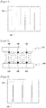
- the electrochromic device (100) related to the first embodiment comprises a first electrode layer (130), a first electrochromic layer (150) provided on the first electrode layer (130), an electrolyte layer (170) provided on the first electrochromic layer (150), a second electrochromic layer (160) provided on the electrolyte layer (170) and a second electrode layer (140) provided on the second electrochromic layer (160).
- a reference numeral 110 denotes a first substrate on which the first electrode layer (130) is provided and a reference numeral 120 denotes a second substrate on which the second electrode layer (140) is provided.
- the electrochromic device (100) comprises a first auxiliary electrode layer (190) and a second auxiliary electrode layer (180) each provided on each opposite surface of the first electrochromic layer (150) and the second electrochromic layer (160) opposed to each other with the electrolyte layer (170) interposed therebetween.
- the electrochromic device (200) related to an example not according to the invention comprises a first electrode layer (130), a first electrochromic layer (150) provided on the first electrode layer (130), an electrolyte layer (170) provided on the first electrochromic layer (150), a second electrochromic layer (160) provided on the electrolyte layer (170) and a second electrode layer (140) provided on the second electrochromic layer (160).
- the electrochromic device (200) comprises a first auxiliary electrode layer (190) and a second auxiliary electrode layer (180) each provided on each opposite surface of the first electrode layer (130) and the second electrode layer (140) opposed to each other with the electrolyte layer (170) interposed therebetween.
- the electrochromic device (100) of the first embodiment and the electrochromic device (200) of the example differ only at the positions where the first auxiliary electrode layer (190) and the second auxiliary electrode layer (180) are formed. That is, in Figures 1 and 2 , the components indicated by the same reference numerals are the same.
- the first substrate (110) and the second substrate (120) may be formed of glass or a polymer resin (for example, PET, PES, or the like).
- the first and second electrode layers (130, 140) are a component for supplying electric charges to the electrochromic layers (150, 170), where each can be formed by comprising any one of a transparent conductive oxide selected from the group consisting of ITO (Indium Tin Oxide), FTO (Fluor doped Tin Oxide), AZO (Aluminium doped Zinc Oxide), GZO (Galium doped Zinc Oxide), ATO (Antimony doped Tin Oxide), IZO (Indium doped Zinc Oxide), NTO (Niobium doped Titanium Oxide), ZnO, OMO (Oxide/Metal/Oxide) and CTO; silver (Ag) nanowires; metal meshes; or OMO (oxide metal oxide).
- the first and second electrode layers (130, 140) are each a transparent electrode layer, which can be formed by comprising a material having a high transmittance to light, a low sheet resistance and a permeation resistance, and can be composed of an electrode plate shape.
- each of the electrode layers (150, 170) is not particularly limited, and any known method may be used without limitation.
- a thin film electrode layer containing transparent conductive oxide particles can be formed on a glass base layer through a process such as sputtering or printing (screen printing, gravure printing, inkjet printing, etc.).
- the electrode layer thus prepared may have a thickness in a range of 10 nm to 500 nm in the case of the vacuum method, and may have a thickness in a range of 0.1 ⁇ m to 20 ⁇ m in the case of the printing method.
- the electrochromic device comprising the electrode layer may have a transmittance for visible light of 70% to 95%.
- the first electrochromic layer (150) may comprise a discoloring material having a chromogenic property complementary to that of the electrochromic material contained in the second electrochromic layer (160).
- the complementary chromogenic property refers to a case where the types of reactions in which the electrochromic material can be colored are different from each other, and for example, it means a case where the reductive discoloring material is used in the first electrochromic layer (150), when the oxidative discoloring material is used in the second electrochromic layer (160).
- the discoloring material having the complementary chromogenic property is contained in the first electrochromic layer (150) and the second electrochromic layer (160), respectively, for example, the coloring of the first electrochromic layer (150) by the reduction reaction and the coloring of the second electrochromic layer (160) by the oxidation reaction can be performed at the same time, and in the contrary case, the decoloring of the first electrochromic layer (150) and the second electrochromic layer (160) can be performed at the same time. As a result, coloring and decoloring of the entire device can be performed at the same time.
- the coloring and decoloring as above may be alternated according to the polarity of the voltage applied to the device.
- the first electrochromic layer (150) may comprise a reductive discoloring material such as tungsten oxide (WOx) as an electrochromic material.
- a reductive discoloring material such as tungsten oxide (WOx)
- the method of forming the first and second electrochromic layers (150, 170) comprising the electrochromic material is not particularly limited and may be performed by, for example, vapor deposition.
- the oxidative discoloring material may mean a material that is discolored when an oxidation reaction occurs
- the reductive discoloring material may mean a material that is discolored when a reduction reaction occurs.
- an oxide of Co, Rh, Ir, Ni, Cr, Mn and Fe for example, LiNiO 2 , IrO 2 , NiO, V 2 O 5 , LixCoO 2 , Rh 2 O 3 or CrO 3 and the like is used
- the reductive discoloring material an oxide of Ti, V, Nb, Ta, Mo and W, for example, WO 3 , MoO 3 , Nb 2 O 5 , Ta 2 O 5 or TiO 2 and the like is used, but the discoloring materials of the present application are not limited to the above oxides.
- the type of the electrolyte, used in the electrolyte layer, as a material that provides a moving environment of hydrogen ions or lithium ions for discoloring or decoloring of the electrochromic material is not particularly limited, and a liquid electrolyte, a gel polymer electrolyte or an inorganic solid electrolyte may be used.
- the electrolyte may comprise one or more compounds, for example, of compounds comprising H + , Li + , Na + , K + , Rb + , or Cs + .
- the electrolyte layer may comprise a lithium salt compound such as LiClO 4 , LiBF 4 , LiAsF 6 , or LiPF 6 .
- the ions included in the electrolyte may play a part in discoloration or light transmittance change of the device while being inserted into or removed from the first electrochromic layer (150) or the first electrochromic layer (170) depending on the polarity of the applied voltage.
- the electrolyte may further comprise a carbonate compound. Since the carbonate-based compound has a high dielectric constant, the ion conductivity provided by the lithium salt can be increased.
- the carbonate-based compound at least one of PC (propylene carbonate), EC (ethylene carbonate), DMC (dimethyl carbonate), DEC (diethyl carbonate) and EMC (ethylmethyl carbonate) may be used.
- the electrolyte when used in the electrolyte layer, the electrolyte may comprise LiPON or Ta 2 O 5 . Furthermore, the inorganic solid electrolyte may be an electrolyte in which components such as B, S, and W are added to LiPON or Ta 2 O 5 .
- the electrochromic devices (100, 200) may further comprise a power source (driving part) for applying a voltage to the electrochromic layers (150, 170).
- first and second auxiliary electrode layers (190, 180) may be each formed of a metal material having a high electrical conductivity, and for example, may be formed of a material having high electrical conductivity such as silver (Ag) or copper (Cu).
- first auxiliary electrode layer (190) and the second auxiliary electrode layer (180) may each have a metal mesh or metal strip pattern.
- the metal mesh pattern may include a first component extending in a first direction and a second component extending in a second direction to intersect the first component. At this time, it has a plurality of openings by the cross structure of pluralities of first and second components.
- the metal strip has a strip shape extending in one direction.
- first auxiliary electrode layer (190) and the second auxiliary electrode layer (180) may each comprise an electrode portion of a metal material and an insulation portion for insulating the electrode portion to prevent elution of the electrode portion upon operating the electrochromic devices (100, 200). Specifically, due to permeation of ions or electrons, a problem of elution of the electrode portion may occur.
- the insulation portion may have a layer structure surrounding the electrode portion. For example, in Figure 1 , the insulation portion may surround the electrode portion so as to insulate the electrode portion from the electrolyte layer (170). In addition, in Figure 2 , the insulation portion may surround the electrode portion so as to insulate the electrode portion from the first and second electrochromic layers (150, 170), respectively.
- the insulation portion may be composed by comprising a resin material as a material that can prevent permeation of ions or electrons.
- the insulation portion may be formed of, for example, a resin of acrylate or epoxy series, and the insulation portion may further comprise an inorganic filler or an inorganic filling agent.
- the first and second auxiliary electrode layers (190, 180) are arranged asymmetrically on the basis of the electrolyte layer (170). That is, the first and second auxiliary electrode layers (190, 180) are arranged to be staggered on the basis of the electrolyte layer (170).
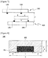
- Figure 4 is a plan view of Figure 3 and Figure 6 is a plan view of Figure 5 , where Figures 3 and 5 differ in the degree of staggering between the first and second auxiliary electrode layers (190, 180).
- a reference numeral 300 denotes a second electrode layer or a second electrochromic layer
- a reference numeral 400 denotes a first electrode layer or a first electrochromic layer.
- a (pitch), b (horizontal interval) and c may be each 10 cm or less, d (vertical interval) may be 0.1 cm or less, b/c may be 0.3 to 3, and a/c may be 2 or more. That is, the first and second auxiliary electrode layers (190, 180) may be each provided to satisfy at least one of the above numerical ranges.
- the electrochromic devices (100, 200) may be provided to have an aperture ratio of about 50 to 95% and a transmittance of about 40 to 93% in consideration of the formation area of the first and second auxiliary electrode layers (190, 180).
- FIG 8 is a conceptual diagram showing a second auxiliary electrode layer (180). As described above, since the first and second auxiliary electrode layers (190, 180) have the same structure, the second auxiliary electrode layer will be described as an example.
- a (width of the insulation portion) may be 5 mm or less
- b, c (width of the electrode portion) and d may be each 3 mm or less
- e (thickness of the electrode portion) may be 1 mm or less
- f (thickness of the insulation portion) may be 2 mm or less.
- c/a may be 0.9 or less
- b/d may be 1.5 or less.
- the reaction rate of the electrochromic device can be improved by arranging first and second auxiliary electrodes to be staggered.
Landscapes
- Physics & Mathematics (AREA)
- Nonlinear Science (AREA)
- General Physics & Mathematics (AREA)
- Optics & Photonics (AREA)
- Electrochromic Elements, Electrophoresis, Or Variable Reflection Or Absorption Elements (AREA)
Claims (7)
- Elektrochrome Vorrichtung (100) aufweisend:eine erste Elektrodenschicht (130);eine erste elektrochrome Schicht (150), die auf der ersten Elektrodenschicht (130) bereitgestellt ist;eine Elektrolytschicht (170), die auf der ersten elektrochromen Schicht (150) bereitgestellt ist;eine zweite elektrochrome Schicht (160), die auf der Elektrolytschicht (170) bereitgestellt ist;eine zweite Elektrodenschicht (140), die auf der zweiten elektrochromen Schicht (160) bereitgestellt ist; undeine erste Zusatzelektrodenschicht (190) und eine zweite Zusatzelektrodenschicht (180) wobei die Elektrolytschicht (170) dazwischen angeordnet ist, wobei die erste Zusatzelektrodenschicht (190) auf einer Oberfläche der ersten elektrochromen Schicht (150) bereitgestellt und die zweite Zusatzelektrodenschicht (180) auf einer Oberfläche der zweiten elektrochromen Schicht (160) bereitgestellt sind, wobei die Oberflächen der ersten elektrochromen Schicht (150) und der zweiten elektrochromen Schicht (160) einander zugewandt sind,wobei die erste Zusatzelektrodenschicht erste Zusatzelektroden aufweisen und die zweite Zusatzelektrodenschicht zweite Zusatzelektroden aufweisen und dadurch gekennzeichnet sind, dass die ersten Zusatzelektroden (180) und die zweiten Zusatzelektroden (190) so angeordnet sind, dass sie bezüglich der Elektrolytschicht (170) gestaffelt sind.
- Elektrochrome Vorrichtung nach Anspruch 1,
wobei die erste Zusatzelektrodenschicht (180) und die zweite Zusatzelektrodenschicht (190) in einer Metallgitterstruktur oder Metallstreifenstruktur ausgebildet sind. - Elektrochrome Vorrichtung nach einem der Ansprüche 1 bis 2,
wobei die ersten Zusatzelektroden (180) und die zweiten Zusatzelektroden (190) jeweils einen Elektrodenabschnitt (181), der aus einem Metallmaterial gebildet ist, und einen Isolierabschnitt (182) aufweisen, der den Elektrodenabschnitt (181) umgibt, um den Elektrodenabschnitt (181) zu isolieren. - Elektrochrome Vorrichtung nach Anspruch 3,
wobei der Isolationsabschnitt (182) aus einem Harzmaterial gebildet ist. - Elektrochrome Vorrichtung nach Anspruch 3 oder 4,
wobei der Isolationsabschnitt (182) aus einem Harz der Acrylat- oder Epoxidreihe gebildet ist. - Elektrochrome Vorrichtung nach einem der Ansprüche 5,
wobei der Isolationsabschnitt (182) ferner einen anorganischen Füllstoff oder ein anorganisches Füllmittel umfasst. - Elektrochrome Vorrichtung nach einem der Ansprüche 3 bis 6,
wobei der Isolationsabschnitt (182) eine Breite von 5 mm oder weniger und eine Dicke von 2 mm oder weniger aufweist, und
wobei der Elektrodenabschnitt (181) eine Breite von 3 mm oder weniger und eine Dicke von 1 mm oder weniger aufweist.
Applications Claiming Priority (2)
| Application Number | Priority Date | Filing Date | Title |
|---|---|---|---|
| KR1020160056302A KR102141635B1 (ko) | 2016-05-09 | 2016-05-09 | 전기변색소자 |
| PCT/KR2017/004753 WO2017196036A1 (ko) | 2016-05-09 | 2017-05-08 | 전기변색소자 |
Publications (3)
| Publication Number | Publication Date |
|---|---|
| EP3457205A4 EP3457205A4 (de) | 2019-03-20 |
| EP3457205A1 EP3457205A1 (de) | 2019-03-20 |
| EP3457205B1 true EP3457205B1 (de) | 2021-04-21 |
Family
ID=60266590
Family Applications (1)
| Application Number | Title | Priority Date | Filing Date |
|---|---|---|---|
| EP17796336.0A Active EP3457205B1 (de) | 2016-05-09 | 2017-05-08 | Elektrochromes element |
Country Status (6)
| Country | Link |
|---|---|
| US (1) | US10871696B2 (de) |
| EP (1) | EP3457205B1 (de) |
| JP (1) | JP6851677B2 (de) |
| KR (1) | KR102141635B1 (de) |
| CN (1) | CN108780259A (de) |
| WO (1) | WO2017196036A1 (de) |
Families Citing this family (11)
| Publication number | Priority date | Publication date | Assignee | Title |
|---|---|---|---|---|
| KR102141636B1 (ko) * | 2016-05-09 | 2020-08-05 | 주식회사 엘지화학 | 전기변색소자 |
| KR20170140530A (ko) * | 2016-06-13 | 2017-12-21 | 주식회사 엘지화학 | 전기변색소자 |
| KR101999352B1 (ko) * | 2017-12-15 | 2019-07-11 | 성문전자주식회사 | 투과율이 가변되는 스마트 윈도우용 변색필름 |
| KR101986348B1 (ko) * | 2017-12-15 | 2019-06-05 | 성문전자주식회사 | 이색이상의 다변색이 가능한 스마트 윈도우용 변색필름 |
| KR102139829B1 (ko) * | 2018-12-28 | 2020-07-31 | 주식회사 스위스 | 전기 변색 효율 및 시간을 개선한 전기 변색 소자와 그 제조 방법 |
| KR102101866B1 (ko) * | 2019-09-11 | 2020-04-20 | 주식회사 스위스 | 플랙서블 전기변색소자의 제조방법 |
| KR102101874B1 (ko) * | 2019-09-11 | 2020-04-20 | 주식회사 스위스 | 저항이 낮은 투명전극 구조를 가지는 전기변색소자 |
| US11966139B2 (en) * | 2020-07-31 | 2024-04-23 | Ricoh Company, Ltd. | Electrochromic element, and method for driving the same |
| CN111880348B (zh) * | 2020-08-07 | 2023-04-28 | 中国科学院广州能源研究所 | 一种新型电致变色器件及其制备方法 |
| CN112764286B (zh) * | 2021-01-29 | 2023-07-07 | 哈尔滨工业大学 | 一种智能调控红外发射率的热控器件及其制备方法 |
| CN114089573A (zh) * | 2021-11-25 | 2022-02-25 | 业成科技(成都)有限公司 | 电致变色元件及变色玻璃、透明显示屏 |
Citations (1)
| Publication number | Priority date | Publication date | Assignee | Title |
|---|---|---|---|---|
| JPS6490422A (en) * | 1987-09-30 | 1989-04-06 | Sekisui Chemical Co Ltd | Electrochromic element |
Family Cites Families (18)
| Publication number | Priority date | Publication date | Assignee | Title |
|---|---|---|---|---|
| JPH0693067B2 (ja) * | 1985-12-17 | 1994-11-16 | 旭硝子株式会社 | 調光体 |
| JPH01142927U (de) * | 1988-03-25 | 1989-09-29 | ||
| JPH01259325A (ja) * | 1988-04-08 | 1989-10-17 | Toyoda Gosei Co Ltd | エレクトロクロミック調光板 |
| JPH08335472A (ja) * | 1995-06-08 | 1996-12-17 | Shin Etsu Polymer Co Ltd | ヒートシールコネクタ |
| US20070076286A1 (en) * | 2005-09-23 | 2007-04-05 | Yungeun Sung | Electrochromic device comprising protective inorganic solid electrolyte film and manufacturing method thereof |
| JP2009084350A (ja) * | 2007-09-28 | 2009-04-23 | Toyobo Co Ltd | 活性光線硬化型樹脂組成物、インキ、およびこれを塗布した積層物 |
| US9664974B2 (en) | 2009-03-31 | 2017-05-30 | View, Inc. | Fabrication of low defectivity electrochromic devices |
| CA2797826C (en) * | 2010-04-30 | 2017-10-31 | Soladigm, Inc. | Electrochromic devices |
| KR101841618B1 (ko) | 2010-12-16 | 2018-03-23 | 삼성전자주식회사 | 전기 변색 소자용 잉크, 전기 변색 소자 및 그 제조 방법 |
| JP5719791B2 (ja) * | 2011-03-30 | 2015-05-20 | 富士フイルム株式会社 | プリント配線基板の製造方法 |
| KR101866561B1 (ko) * | 2011-08-04 | 2018-06-11 | 주식회사 두산 | 성형성이 우수한 에폭시 수지 조성물 및 이를 포함한 금속 베이스 인쇄회로기판용 적층체 |
| JP5887024B2 (ja) | 2012-08-08 | 2016-03-16 | キネストラル・テクノロジーズ・インコーポレイテッドKinestral Technologies,Inc. | 複合電気導電層を有したエレクトロクロミック多層デバイス |
| TW201426148A (zh) * | 2012-12-26 | 2014-07-01 | 立得光電科技股份有限公司 | 電致變色結構 |
| US10761393B2 (en) * | 2013-02-04 | 2020-09-01 | E-Vision, Llc | Electro-chromic devices including solid or quasi-solid electrolyte layers and methods of making the same |
| CN105074543B (zh) * | 2013-03-13 | 2018-10-23 | 3M创新有限公司 | 电子可切换的保密装置 |
| KR102108830B1 (ko) * | 2014-01-21 | 2020-05-11 | 엘지이노텍 주식회사 | 전기변색 디바이스 |
| US9869918B2 (en) * | 2015-01-16 | 2018-01-16 | Ricoh Company, Ltd. | Electrochromic apparatus, electrochromic element, and method of manufacturing electrochromic element |
| KR102141636B1 (ko) * | 2016-05-09 | 2020-08-05 | 주식회사 엘지화학 | 전기변색소자 |
-
2016
- 2016-05-09 KR KR1020160056302A patent/KR102141635B1/ko active Active
-
2017
- 2017-05-08 CN CN201780017241.9A patent/CN108780259A/zh active Pending
- 2017-05-08 JP JP2018547367A patent/JP6851677B2/ja active Active
- 2017-05-08 WO PCT/KR2017/004753 patent/WO2017196036A1/ko not_active Ceased
- 2017-05-08 EP EP17796336.0A patent/EP3457205B1/de active Active
- 2017-05-08 US US16/082,045 patent/US10871696B2/en active Active
Patent Citations (1)
| Publication number | Priority date | Publication date | Assignee | Title |
|---|---|---|---|---|
| JPS6490422A (en) * | 1987-09-30 | 1989-04-06 | Sekisui Chemical Co Ltd | Electrochromic element |
Also Published As
| Publication number | Publication date |
|---|---|
| JP2019507910A (ja) | 2019-03-22 |
| KR102141635B1 (ko) | 2020-08-05 |
| EP3457205A4 (de) | 2019-03-20 |
| US20200117066A1 (en) | 2020-04-16 |
| JP6851677B2 (ja) | 2021-03-31 |
| WO2017196036A1 (ko) | 2017-11-16 |
| CN108780259A (zh) | 2018-11-09 |
| KR20170126207A (ko) | 2017-11-17 |
| EP3457205A1 (de) | 2019-03-20 |
| US10871696B2 (en) | 2020-12-22 |
Similar Documents
| Publication | Publication Date | Title |
|---|---|---|
| US10871696B2 (en) | Electrochromic device | |
| US11099450B2 (en) | Electrochromic device | |
| US10935863B2 (en) | Electrochromic device | |
| CN108369363B (zh) | 电致变色装置 | |
| KR102010755B1 (ko) | 전기변색소자, 전기변색소자의 제조방법 및 그 투과율 제어방법 | |
| KR102056095B1 (ko) | 전기변색소자 | |
| KR102091612B1 (ko) | 변색 반응속도가 개선된 전기 변색소자 및 이의 제조방법 | |
| KR102024255B1 (ko) | 전기변색소자 및 그 제조방법 | |
| KR102079142B1 (ko) | 전기변색소자 | |
| US11194212B2 (en) | Electrochromic device | |
| KR102108562B1 (ko) | 전기변색소자 | |
| KR20230099657A (ko) | 전기변색소자 | |
| KR102071901B1 (ko) | 전기변색소자 | |
| KR102069486B1 (ko) | 전기변색소자 |
Legal Events
| Date | Code | Title | Description |
|---|---|---|---|
| STAA | Information on the status of an ep patent application or granted ep patent |
Free format text: STATUS: THE INTERNATIONAL PUBLICATION HAS BEEN MADE |
|
| PUAI | Public reference made under article 153(3) epc to a published international application that has entered the european phase |
Free format text: ORIGINAL CODE: 0009012 |
|
| STAA | Information on the status of an ep patent application or granted ep patent |
Free format text: STATUS: REQUEST FOR EXAMINATION WAS MADE |
|
| 17P | Request for examination filed |
Effective date: 20180830 |
|
| A4 | Supplementary search report drawn up and despatched |
Effective date: 20190219 |
|
| AK | Designated contracting states |
Kind code of ref document: A1 Designated state(s): AL AT BE BG CH CY CZ DE DK EE ES FI FR GB GR HR HU IE IS IT LI LT LU LV MC MK MT NL NO PL PT RO RS SE SI SK SM TR |
|
| AX | Request for extension of the european patent |
Extension state: BA ME |
|
| DAV | Request for validation of the european patent (deleted) | ||
| DAX | Request for extension of the european patent (deleted) | ||
| STAA | Information on the status of an ep patent application or granted ep patent |
Free format text: STATUS: EXAMINATION IS IN PROGRESS |
|
| 17Q | First examination report despatched |
Effective date: 20200525 |
|
| GRAP | Despatch of communication of intention to grant a patent |
Free format text: ORIGINAL CODE: EPIDOSNIGR1 |
|
| STAA | Information on the status of an ep patent application or granted ep patent |
Free format text: STATUS: GRANT OF PATENT IS INTENDED |
|
| INTG | Intention to grant announced |
Effective date: 20210205 |
|
| GRAS | Grant fee paid |
Free format text: ORIGINAL CODE: EPIDOSNIGR3 |
|
| GRAA | (expected) grant |
Free format text: ORIGINAL CODE: 0009210 |
|
| STAA | Information on the status of an ep patent application or granted ep patent |
Free format text: STATUS: THE PATENT HAS BEEN GRANTED |
|
| AK | Designated contracting states |
Kind code of ref document: B1 Designated state(s): AL AT BE BG CH CY CZ DE DK EE ES FI FR GB GR HR HU IE IS IT LI LT LU LV MC MK MT NL NO PL PT RO RS SE SI SK SM TR |
|
| REG | Reference to a national code |
Ref country code: GB Ref legal event code: FG4D |
|
| REG | Reference to a national code |
Ref country code: CH Ref legal event code: EP |
|
| REG | Reference to a national code |
Ref country code: DE Ref legal event code: R096 Ref document number: 602017037225 Country of ref document: DE Ref country code: IE Ref legal event code: FG4D |
|
| REG | Reference to a national code |
Ref country code: AT Ref legal event code: REF Ref document number: 1385266 Country of ref document: AT Kind code of ref document: T Effective date: 20210515 |
|
| REG | Reference to a national code |
Ref country code: LT Ref legal event code: MG9D |
|
| REG | Reference to a national code |
Ref country code: AT Ref legal event code: MK05 Ref document number: 1385266 Country of ref document: AT Kind code of ref document: T Effective date: 20210421 |
|
| REG | Reference to a national code |
Ref country code: NL Ref legal event code: MP Effective date: 20210421 |
|
| PG25 | Lapsed in a contracting state [announced via postgrant information from national office to epo] |
Ref country code: LT Free format text: LAPSE BECAUSE OF FAILURE TO SUBMIT A TRANSLATION OF THE DESCRIPTION OR TO PAY THE FEE WITHIN THE PRESCRIBED TIME-LIMIT Effective date: 20210421 Ref country code: FI Free format text: LAPSE BECAUSE OF FAILURE TO SUBMIT A TRANSLATION OF THE DESCRIPTION OR TO PAY THE FEE WITHIN THE PRESCRIBED TIME-LIMIT Effective date: 20210421 Ref country code: HR Free format text: LAPSE BECAUSE OF FAILURE TO SUBMIT A TRANSLATION OF THE DESCRIPTION OR TO PAY THE FEE WITHIN THE PRESCRIBED TIME-LIMIT Effective date: 20210421 Ref country code: AT Free format text: LAPSE BECAUSE OF FAILURE TO SUBMIT A TRANSLATION OF THE DESCRIPTION OR TO PAY THE FEE WITHIN THE PRESCRIBED TIME-LIMIT Effective date: 20210421 Ref country code: BG Free format text: LAPSE BECAUSE OF FAILURE TO SUBMIT A TRANSLATION OF THE DESCRIPTION OR TO PAY THE FEE WITHIN THE PRESCRIBED TIME-LIMIT Effective date: 20210721 Ref country code: NL Free format text: LAPSE BECAUSE OF FAILURE TO SUBMIT A TRANSLATION OF THE DESCRIPTION OR TO PAY THE FEE WITHIN THE PRESCRIBED TIME-LIMIT Effective date: 20210421 |
|
| PG25 | Lapsed in a contracting state [announced via postgrant information from national office to epo] |
Ref country code: PL Free format text: LAPSE BECAUSE OF FAILURE TO SUBMIT A TRANSLATION OF THE DESCRIPTION OR TO PAY THE FEE WITHIN THE PRESCRIBED TIME-LIMIT Effective date: 20210421 Ref country code: NO Free format text: LAPSE BECAUSE OF FAILURE TO SUBMIT A TRANSLATION OF THE DESCRIPTION OR TO PAY THE FEE WITHIN THE PRESCRIBED TIME-LIMIT Effective date: 20210721 Ref country code: PT Free format text: LAPSE BECAUSE OF FAILURE TO SUBMIT A TRANSLATION OF THE DESCRIPTION OR TO PAY THE FEE WITHIN THE PRESCRIBED TIME-LIMIT Effective date: 20210823 Ref country code: LV Free format text: LAPSE BECAUSE OF FAILURE TO SUBMIT A TRANSLATION OF THE DESCRIPTION OR TO PAY THE FEE WITHIN THE PRESCRIBED TIME-LIMIT Effective date: 20210421 Ref country code: RS Free format text: LAPSE BECAUSE OF FAILURE TO SUBMIT A TRANSLATION OF THE DESCRIPTION OR TO PAY THE FEE WITHIN THE PRESCRIBED TIME-LIMIT Effective date: 20210421 Ref country code: SE Free format text: LAPSE BECAUSE OF FAILURE TO SUBMIT A TRANSLATION OF THE DESCRIPTION OR TO PAY THE FEE WITHIN THE PRESCRIBED TIME-LIMIT Effective date: 20210421 Ref country code: GR Free format text: LAPSE BECAUSE OF FAILURE TO SUBMIT A TRANSLATION OF THE DESCRIPTION OR TO PAY THE FEE WITHIN THE PRESCRIBED TIME-LIMIT Effective date: 20210722 Ref country code: IS Free format text: LAPSE BECAUSE OF FAILURE TO SUBMIT A TRANSLATION OF THE DESCRIPTION OR TO PAY THE FEE WITHIN THE PRESCRIBED TIME-LIMIT Effective date: 20210821 |
|
| REG | Reference to a national code |
Ref country code: CH Ref legal event code: PL |
|
| REG | Reference to a national code |
Ref country code: DE Ref legal event code: R097 Ref document number: 602017037225 Country of ref document: DE |
|
| PG25 | Lapsed in a contracting state [announced via postgrant information from national office to epo] |
Ref country code: SK Free format text: LAPSE BECAUSE OF FAILURE TO SUBMIT A TRANSLATION OF THE DESCRIPTION OR TO PAY THE FEE WITHIN THE PRESCRIBED TIME-LIMIT Effective date: 20210421 Ref country code: SM Free format text: LAPSE BECAUSE OF FAILURE TO SUBMIT A TRANSLATION OF THE DESCRIPTION OR TO PAY THE FEE WITHIN THE PRESCRIBED TIME-LIMIT Effective date: 20210421 Ref country code: RO Free format text: LAPSE BECAUSE OF FAILURE TO SUBMIT A TRANSLATION OF THE DESCRIPTION OR TO PAY THE FEE WITHIN THE PRESCRIBED TIME-LIMIT Effective date: 20210421 Ref country code: ES Free format text: LAPSE BECAUSE OF FAILURE TO SUBMIT A TRANSLATION OF THE DESCRIPTION OR TO PAY THE FEE WITHIN THE PRESCRIBED TIME-LIMIT Effective date: 20210421 Ref country code: EE Free format text: LAPSE BECAUSE OF FAILURE TO SUBMIT A TRANSLATION OF THE DESCRIPTION OR TO PAY THE FEE WITHIN THE PRESCRIBED TIME-LIMIT Effective date: 20210421 Ref country code: CH Free format text: LAPSE BECAUSE OF NON-PAYMENT OF DUE FEES Effective date: 20210531 Ref country code: DK Free format text: LAPSE BECAUSE OF FAILURE TO SUBMIT A TRANSLATION OF THE DESCRIPTION OR TO PAY THE FEE WITHIN THE PRESCRIBED TIME-LIMIT Effective date: 20210421 Ref country code: CZ Free format text: LAPSE BECAUSE OF FAILURE TO SUBMIT A TRANSLATION OF THE DESCRIPTION OR TO PAY THE FEE WITHIN THE PRESCRIBED TIME-LIMIT Effective date: 20210421 Ref country code: LU Free format text: LAPSE BECAUSE OF NON-PAYMENT OF DUE FEES Effective date: 20210508 Ref country code: LI Free format text: LAPSE BECAUSE OF NON-PAYMENT OF DUE FEES Effective date: 20210531 Ref country code: MC Free format text: LAPSE BECAUSE OF FAILURE TO SUBMIT A TRANSLATION OF THE DESCRIPTION OR TO PAY THE FEE WITHIN THE PRESCRIBED TIME-LIMIT Effective date: 20210421 |
|
| REG | Reference to a national code |
Ref country code: BE Ref legal event code: MM Effective date: 20210531 |
|
| PLBE | No opposition filed within time limit |
Free format text: ORIGINAL CODE: 0009261 |
|
| STAA | Information on the status of an ep patent application or granted ep patent |
Free format text: STATUS: NO OPPOSITION FILED WITHIN TIME LIMIT |
|
| 26N | No opposition filed |
Effective date: 20220124 |
|
| PG25 | Lapsed in a contracting state [announced via postgrant information from national office to epo] |
Ref country code: IE Free format text: LAPSE BECAUSE OF NON-PAYMENT OF DUE FEES Effective date: 20210508 |
|
| PG25 | Lapsed in a contracting state [announced via postgrant information from national office to epo] |
Ref country code: IS Free format text: LAPSE BECAUSE OF FAILURE TO SUBMIT A TRANSLATION OF THE DESCRIPTION OR TO PAY THE FEE WITHIN THE PRESCRIBED TIME-LIMIT Effective date: 20210821 Ref country code: AL Free format text: LAPSE BECAUSE OF FAILURE TO SUBMIT A TRANSLATION OF THE DESCRIPTION OR TO PAY THE FEE WITHIN THE PRESCRIBED TIME-LIMIT Effective date: 20210421 |
|
| PG25 | Lapsed in a contracting state [announced via postgrant information from national office to epo] |
Ref country code: IT Free format text: LAPSE BECAUSE OF FAILURE TO SUBMIT A TRANSLATION OF THE DESCRIPTION OR TO PAY THE FEE WITHIN THE PRESCRIBED TIME-LIMIT Effective date: 20210421 Ref country code: BE Free format text: LAPSE BECAUSE OF NON-PAYMENT OF DUE FEES Effective date: 20210531 |
|
| PG25 | Lapsed in a contracting state [announced via postgrant information from national office to epo] |
Ref country code: CY Free format text: LAPSE BECAUSE OF FAILURE TO SUBMIT A TRANSLATION OF THE DESCRIPTION OR TO PAY THE FEE WITHIN THE PRESCRIBED TIME-LIMIT Effective date: 20210421 |
|
| PG25 | Lapsed in a contracting state [announced via postgrant information from national office to epo] |
Ref country code: HU Free format text: LAPSE BECAUSE OF FAILURE TO SUBMIT A TRANSLATION OF THE DESCRIPTION OR TO PAY THE FEE WITHIN THE PRESCRIBED TIME-LIMIT; INVALID AB INITIO Effective date: 20170508 |
|
| PG25 | Lapsed in a contracting state [announced via postgrant information from national office to epo] |
Ref country code: MK Free format text: LAPSE BECAUSE OF FAILURE TO SUBMIT A TRANSLATION OF THE DESCRIPTION OR TO PAY THE FEE WITHIN THE PRESCRIBED TIME-LIMIT Effective date: 20210421 |
|
| PG25 | Lapsed in a contracting state [announced via postgrant information from national office to epo] |
Ref country code: TR Free format text: LAPSE BECAUSE OF FAILURE TO SUBMIT A TRANSLATION OF THE DESCRIPTION OR TO PAY THE FEE WITHIN THE PRESCRIBED TIME-LIMIT Effective date: 20210421 |
|
| PG25 | Lapsed in a contracting state [announced via postgrant information from national office to epo] |
Ref country code: MT Free format text: LAPSE BECAUSE OF FAILURE TO SUBMIT A TRANSLATION OF THE DESCRIPTION OR TO PAY THE FEE WITHIN THE PRESCRIBED TIME-LIMIT Effective date: 20210421 |
|
| PGFP | Annual fee paid to national office [announced via postgrant information from national office to epo] |
Ref country code: DE Payment date: 20250422 Year of fee payment: 9 |
|
| PGFP | Annual fee paid to national office [announced via postgrant information from national office to epo] |
Ref country code: FR Payment date: 20250422 Year of fee payment: 9 |
|
| PGFP | Annual fee paid to national office [announced via postgrant information from national office to epo] |
Ref country code: GB Payment date: 20260324 Year of fee payment: 10 |