EP3465778B1 - Procédé de réalisation de délaminage de film polymère - Google Patents
Procédé de réalisation de délaminage de film polymère Download PDFInfo
- Publication number
- EP3465778B1 EP3465778B1 EP16904774.3A EP16904774A EP3465778B1 EP 3465778 B1 EP3465778 B1 EP 3465778B1 EP 16904774 A EP16904774 A EP 16904774A EP 3465778 B1 EP3465778 B1 EP 3465778B1
- Authority
- EP
- European Patent Office
- Prior art keywords
- light
- polymer film
- layer
- material layer
- carrier plate
- Prior art date
- Legal status (The legal status is an assumption and is not a legal conclusion. Google has not performed a legal analysis and makes no representation as to the accuracy of the status listed.)
- Active
Links
Images


Classifications
-
- B—PERFORMING OPERATIONS; TRANSPORTING
- B29—WORKING OF PLASTICS; WORKING OF SUBSTANCES IN A PLASTIC STATE IN GENERAL
- B29C—SHAPING OR JOINING OF PLASTICS; SHAPING OF MATERIAL IN A PLASTIC STATE, NOT OTHERWISE PROVIDED FOR; AFTER-TREATMENT OF THE SHAPED PRODUCTS, e.g. REPAIRING
- B29C41/00—Shaping by coating a mould, core or other substrate, i.e. by depositing material and stripping-off the shaped article; Apparatus therefor
- B29C41/02—Shaping by coating a mould, core or other substrate, i.e. by depositing material and stripping-off the shaped article; Apparatus therefor for making articles of definite length, i.e. discrete articles
-
- H—ELECTRICITY
- H10—SEMICONDUCTOR DEVICES; ELECTRIC SOLID-STATE DEVICES NOT OTHERWISE PROVIDED FOR
- H10P—GENERIC PROCESSES OR APPARATUS FOR THE MANUFACTURE OR TREATMENT OF DEVICES COVERED BY CLASS H10
- H10P54/00—Cutting or separating of wafers, substrates or parts of devices
-
- B—PERFORMING OPERATIONS; TRANSPORTING
- B32—LAYERED PRODUCTS
- B32B—LAYERED PRODUCTS, i.e. PRODUCTS BUILT-UP OF STRATA OF FLAT OR NON-FLAT, e.g. CELLULAR OR HONEYCOMB, FORM
- B32B43/00—Operations specially adapted for layered products and not otherwise provided for, e.g. repairing; Apparatus therefor
- B32B43/006—Delaminating
-
- B—PERFORMING OPERATIONS; TRANSPORTING
- B29—WORKING OF PLASTICS; WORKING OF SUBSTANCES IN A PLASTIC STATE IN GENERAL
- B29C—SHAPING OR JOINING OF PLASTICS; SHAPING OF MATERIAL IN A PLASTIC STATE, NOT OTHERWISE PROVIDED FOR; AFTER-TREATMENT OF THE SHAPED PRODUCTS, e.g. REPAIRING
- B29C41/00—Shaping by coating a mould, core or other substrate, i.e. by depositing material and stripping-off the shaped article; Apparatus therefor
- B29C41/34—Component parts, details or accessories; Auxiliary operations
- B29C41/42—Removing articles from moulds, cores or other substrates
-
- B—PERFORMING OPERATIONS; TRANSPORTING
- B32—LAYERED PRODUCTS
- B32B—LAYERED PRODUCTS, i.e. PRODUCTS BUILT-UP OF STRATA OF FLAT OR NON-FLAT, e.g. CELLULAR OR HONEYCOMB, FORM
- B32B7/00—Layered products characterised by the relation between layers; Layered products characterised by the relative orientation of features between layers, or by the relative values of a measurable parameter between layers, i.e. products comprising layers having different physical, chemical or physicochemical properties; Layered products characterised by the interconnection of layers
-
- B—PERFORMING OPERATIONS; TRANSPORTING
- B32—LAYERED PRODUCTS
- B32B—LAYERED PRODUCTS, i.e. PRODUCTS BUILT-UP OF STRATA OF FLAT OR NON-FLAT, e.g. CELLULAR OR HONEYCOMB, FORM
- B32B7/00—Layered products characterised by the relation between layers; Layered products characterised by the relative orientation of features between layers, or by the relative values of a measurable parameter between layers, i.e. products comprising layers having different physical, chemical or physicochemical properties; Layered products characterised by the interconnection of layers
- B32B7/04—Interconnection of layers
- B32B7/06—Interconnection of layers permitting easy separation
-
- H—ELECTRICITY
- H10—SEMICONDUCTOR DEVICES; ELECTRIC SOLID-STATE DEVICES NOT OTHERWISE PROVIDED FOR
- H10F—INORGANIC SEMICONDUCTOR DEVICES SENSITIVE TO INFRARED RADIATION, LIGHT, ELECTROMAGNETIC RADIATION OF SHORTER WAVELENGTH OR CORPUSCULAR RADIATION
- H10F71/00—Manufacture or treatment of devices covered by this subclass
-
- H—ELECTRICITY
- H10—SEMICONDUCTOR DEVICES; ELECTRIC SOLID-STATE DEVICES NOT OTHERWISE PROVIDED FOR
- H10F—INORGANIC SEMICONDUCTOR DEVICES SENSITIVE TO INFRARED RADIATION, LIGHT, ELECTROMAGNETIC RADIATION OF SHORTER WAVELENGTH OR CORPUSCULAR RADIATION
- H10F77/00—Constructional details of devices covered by this subclass
- H10F77/10—Semiconductor bodies
- H10F77/16—Material structures, e.g. crystalline structures, film structures or crystal plane orientations
- H10F77/169—Thin semiconductor films on metallic or insulating substrates
-
- H—ELECTRICITY
- H10—SEMICONDUCTOR DEVICES; ELECTRIC SOLID-STATE DEVICES NOT OTHERWISE PROVIDED FOR
- H10F—INORGANIC SEMICONDUCTOR DEVICES SENSITIVE TO INFRARED RADIATION, LIGHT, ELECTROMAGNETIC RADIATION OF SHORTER WAVELENGTH OR CORPUSCULAR RADIATION
- H10F77/00—Constructional details of devices covered by this subclass
- H10F77/40—Optical elements or arrangements
- H10F77/413—Optical elements or arrangements directly associated or integrated with the devices, e.g. back reflectors
-
- H—ELECTRICITY
- H10—SEMICONDUCTOR DEVICES; ELECTRIC SOLID-STATE DEVICES NOT OTHERWISE PROVIDED FOR
- H10P—GENERIC PROCESSES OR APPARATUS FOR THE MANUFACTURE OR TREATMENT OF DEVICES COVERED BY CLASS H10
- H10P14/00—Formation of materials, e.g. in the shape of layers or pillars
- H10P14/20—Formation of materials, e.g. in the shape of layers or pillars of semiconductor materials
- H10P14/29—Formation of materials, e.g. in the shape of layers or pillars of semiconductor materials characterised by the substrates
- H10P14/2901—Materials
- H10P14/2922—Materials being non-crystalline insulating materials, e.g. glass or polymers
-
- H—ELECTRICITY
- H10—SEMICONDUCTOR DEVICES; ELECTRIC SOLID-STATE DEVICES NOT OTHERWISE PROVIDED FOR
- H10P—GENERIC PROCESSES OR APPARATUS FOR THE MANUFACTURE OR TREATMENT OF DEVICES COVERED BY CLASS H10
- H10P14/00—Formation of materials, e.g. in the shape of layers or pillars
- H10P14/60—Formation of materials, e.g. in the shape of layers or pillars of insulating materials
- H10P14/63—Formation of materials, e.g. in the shape of layers or pillars of insulating materials characterised by the formation processes
- H10P14/6326—Deposition processes
- H10P14/6328—Deposition from the gas or vapour phase
-
- B—PERFORMING OPERATIONS; TRANSPORTING
- B29—WORKING OF PLASTICS; WORKING OF SUBSTANCES IN A PLASTIC STATE IN GENERAL
- B29L—INDEXING SCHEME ASSOCIATED WITH SUBCLASS B29C, RELATING TO PARTICULAR ARTICLES
- B29L2007/00—Flat articles, e.g. films or sheets
- B29L2007/008—Wide strips, e.g. films, webs
-
- B—PERFORMING OPERATIONS; TRANSPORTING
- B29—WORKING OF PLASTICS; WORKING OF SUBSTANCES IN A PLASTIC STATE IN GENERAL
- B29L—INDEXING SCHEME ASSOCIATED WITH SUBCLASS B29C, RELATING TO PARTICULAR ARTICLES
- B29L2031/00—Other particular articles
- B29L2031/34—Electrical apparatus, e.g. sparking plugs or parts thereof
-
- H—ELECTRICITY
- H10—SEMICONDUCTOR DEVICES; ELECTRIC SOLID-STATE DEVICES NOT OTHERWISE PROVIDED FOR
- H10P—GENERIC PROCESSES OR APPARATUS FOR THE MANUFACTURE OR TREATMENT OF DEVICES COVERED BY CLASS H10
- H10P72/00—Handling or holding of wafers, substrates or devices during manufacture or treatment thereof
- H10P72/70—Handling or holding of wafers, substrates or devices during manufacture or treatment thereof for supporting or gripping
- H10P72/74—Handling or holding of wafers, substrates or devices during manufacture or treatment thereof for supporting or gripping using temporarily an auxiliary support
- H10P72/7402—Wafer tapes, e.g. grinding or dicing support tapes
Definitions
- the present invention relates to thermal processes in general, and, in particular, to a method for performing delamination of a polymer film.
- One method of printing high-resolution electronic structures with registered layers and/or having a well-defined thicknesses is to deposit various layers onto a very flat surface. This can be done by depositing a polymer film onto a rigid, flat carrier plate (substrate) such as glass, and then forming the subsequent layers on top of the polymer film. After the electronic structures have been formed, the polymer film must be removed from the carrier plate.
- EP0858110 discloses a method for performing delamination of a polymer film wherein light is used to heat a light-absorptive material layer in order to release the polymer film from a carrier plate.
- a method for performing delamination of a polymer film according to the invention is defined in the appended claims 1-8.
- a pixelated pattern layer of light-absorptive material is initially deposited onto a carrier plate, and a light-reflective material layer is then deposited on the light-absorptive material layer.
- a polymer film, which is to be delaminated, is deposited on the light-reflecting material layer.
- a pulsed light source is utilized to irradiate through the carrier plate from the side opposite the polymer film to heat the light-absorptive material layer.
- the heated areas of the light-absorptive material layer heat the polymer film through conduction at the interface between the carrier plate stack and the polymer film, thereby generating gas from the polymer film by its thermal decomposition, which allows the polymer film to be released from the carrier plate.
- a surface tension controlled release layer may be deposited on top of the light-reflecting material layer.
- a dynamic release layer may be deposited prior to the polymer film.
- the carrier plate may be made of glass or quartz.
- the polymer film may be made of polyimide.
- the surface tension controlled release layer may be made of ceramic such as silicon nitride or silicon dioxide.
- One method of removing a polymer film from a carrier plate is to first deposit a thermal release layer on the carrier plate before depositing the polymer film. After forming electronic structures on the polymer film, the entire assembly (carrier plate, thermal release layer, polymer film, and electronic structures) are heated to a temperature high enough for the thermal release layer to release the polymer film.
- One disadvantage of this method is that the processing temperature needed to form the electronic structures must be lower than the release temperature of the thermal release layer.
- Another method of removing a polymer film from a carrier plate is to use a pulsed excimer laser such as a XeFl laser at 308 nm.
- the laser beam from the excimer laser is shined through the carrier plate side and focused at an interface between the polymer film and the carrier plate. This process generates a tiny amount of gas that delaminates the polymer film at the interface between the polymer film and the carrier plate.
- the laser beam can be pulsed and scanned to delaminate a larger area.
- the first disadvantage of this method is that excimer lasers tend to be very expensive, and the second disadvantage is that this method has a very low throughput when compared to other methods.
- a carrier plate 11 is partially covered with a layer of light-absorptive material 12.
- carrier plate 11 is at least partially light transparent, and light-absorptive material 12 can be deposited on carrier plate 11 in a pixelated pattern, for example.
- a layer of light-reflective material 13 is deposited on light-absorptive material layer 12, which renders the portions of carrier plate 11 not covered by light-absorptive material layer 12 to be reflective as viewed from the top of carrier plate 11, as shown in Figure 2 .
- a polymer film 14 is then deposited on light-absorptive material layer 12 and light-reflective material layer 13, followed by the formation of electronic structures (not shown) upon polymer film 14, as shown in Figure 1A .
- Polymer film 14 can be delaminated from carrier plate 11 by illuminating carrier plate 11 from the side opposite polymer film 14 with a light pulse from a flashlamp 19, as shown in Figure 1B .
- the light pulse from flashlamp 19 heats light-absorptive material layer 12, and the heat will transfer to polymer film 14 to generate gas at an interface 21 between light-absorptive material layer 12 and polymer film 14 by decomposing polymer film 14.
- the gas generation level can be controlled at lamp facing side of polymer film 14 to delaminate polymer film 14 from carrier plate 11 without damaging the electronic structures formed upon polymer film 14.
- Additional control of the gas generation can be attained by increasing the intensity and changing the time duration of a light pulse from flashlamp 19.
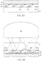
- additional layers may be deposited subsequent to light-absorptive material layer 12 and light-reflective material layer 13, as explained in Figures 3A-3B .
- a carrier plate 31 is partially covered with a first light-absorptive material layer 32a, for example, in a pixelated pattern.
- carrier plate 31 is at least partially light transparent.
- a transparent thermal retardation layer 35 is deposited on light-absorptive material layer 32a.
- Thermal retardation layer 35 is then partially covered with a second light-absorptive material layer 32b, for example, in a pixelated pattern.
- a light-reflective film 33 is deposited on light-absorptive material film 32b, which renders portions of thermal retardation layer 35 not covered by light-absorptive material layer 32b to be reflective as viewed from the top of carrier plate 31, similar to Figure 2 .
- a polymer film 34 is then deposited on second light-absorptive material layer 32b and light-reflective material layer 33, followed by the formation of electronic structures (not shown) upon polymer film 34, as shown in Figure 3A .
- Thermal retardation layer 35 allows additional control in the gas generation because both light-absorptive material layers 32a, 32b are heated at the same time by a single light pulse.
- the heat pulse from carrier plate 31 facing first light-absorptive film 32a is delayed in time from second light-absorptive film 32b that is located closer to polymer film 34.
- the delay in time from the heat pulse creates a zipper effect to delaminate polymer film 34 more gently than that from a single light pulse as shown in Figure IB.
- the same zipper effect to delaminate polymer film 34 from carrier plate 31 mentioned above can also be created by using a gray-scale pixels, where the inner part absorbs most of the light and the outer part absorbs less. During the illumination, phase change will always start at the inner part and propagates outward.
- a surface tension controlled release layer may be deposited on light-reflective material layer 33 before polymer film 34 is deposited.
- a dynamic release layer (not shown) may be deposited before polymer film 34 is deposited.
- the dynamic release layer can be made of a material having a lower phase change temperature than polymer film 34, which helps preventing thermal damage to polymer film 34 from hot light-absorptive material layers 32a, 32b.
- the dynamic release layer can have two different mechanisms as there are two different types of phase changes it can undergo when heated. The first type of phase change is the gasification of the dynamic release layer. The second type is the melting of the dynamic release layer, which results in its de-stabilization due to surface tension.
- polymer film 34 can be released from carrier plate 31.
- the dynamic release layers melts it is preferably made of a material with a low-melting point but with a very high surface tension, such as a metal or metal alloy.
- the dynamic release layer is made of zinc or aluminum.
- a dynamic release layer may be deposited on light-reflective material layer 13 before depositing polymer layer 14.
- a surface tension controlled layer may be deposited upon light-reflective material layer 13 before depositing polymer layer 14.
- Carrier plates 11 and 31 may be made of glass or quartz.
- Light-absorptive material layers 12 and 32a-32b may be made of tungsten.
- Light-reflective material layers 13 and 33 may be made of aluminum.
- Polymer films 14 and 34 may be made of polyimide.
- Thermal retardation layer 36 may be made of silicon oxide or silicon dioxide.
- the surface tension controlled layer may be made of ceramic such as silicon dioxide or silicon nitride.
- the dynamic release layer can be a polymer or a metal with a relatively low melting temperature.
- the present invention provides an improved method for performing delamination of a polymer film.
- An advantage of the method of the present invention over the excimer laser delamination technique is that the light source is very inexpensive ( ⁇ 10X) and delamination area per pulse of light may be much larger ( ⁇ 1,000X) than that of the excimer laser.
Landscapes
- Engineering & Computer Science (AREA)
- Mechanical Engineering (AREA)
- Laminated Bodies (AREA)
- Moulds For Moulding Plastics Or The Like (AREA)
- Manufacturing & Machinery (AREA)
- Formation Of Insulating Films (AREA)
- Thermal Transfer Or Thermal Recording In General (AREA)
Claims (8)
- Procédé de réalisation de délaminage de film polymère, ledit procédé comprenant :le fait de prévoir une plaque de support optiquement transparente (31) ;le dépôt d'une première couche de matériau d'absorption de la lumière (32a) sur ladite plaque de support (31) ;le dépôt d'une couche de retard thermique (35) sur ladite première couche de matériau d'absorption de la lumière (32a) ; caractérisé en ce que le procédé comprendle dépôt d'une seconde couche de matériau d'absorption de la lumière (32b) sur ladite couche de retard thermique (35) ;le dépôt d'une couche de matériau de réflexion de la lumière (33) sur ladite seconde couche de matériau d'absorption de la lumière (32b) ;le dépôt d'un film polymère (34) sur ladite couche de matériau de réflexion de la lumière (32b) et ladite seconde couche de matériau d'absorption de la lumière (33) ;la formation de structures électroniques sur ledit film polymère ; etl'irradiation de ladite plaque de support (31) avec une lumière pulsée afin de chauffer lesdites couches de matériau d'absorption de la lumière afin de libérer ledit film polymère de ladite plaque de support.
- Procédé selon la revendication 1, dans lequel ladite irradiation comprend en outre l'irradiation de ladite plaque de support (31) avec une lampe flash.
- Procédé selon la revendication 1, dans lequel ledit procédé comprend en outre le dépôt d'une couche de séparation à tension de surface contrôlée sur ladite couche de matériau de réflexion de la lumière (32b) avant que ledit film polymère (34) soit déposé.
- Procédé selon la revendication 3, dans lequel ladite couche de séparation à tension de surface contrôlée est composée de céramique.
- Procédé selon la revendication 3, dans lequel ledit procédé comprend en outre le dépôt d'une couche de séparation dynamique sur ladite couche de séparation à tension de surface contrôlée avant que ledit film polymère soit déposé.
- Procédé selon la revendication 5, dans lequel ladite couche de séparation dynamique est composée de métal.
- Procédé selon la revendication 1, dans lequel l'une desdites couches de matériau d'absorption de la lumière est gravée.
- Procédé selon la revendication 1, dans lequel ladite couche de retard thermique (35) est composée d'oxyde de silicium.
Priority Applications (1)
| Application Number | Priority Date | Filing Date | Title |
|---|---|---|---|
| EP20174776.3A EP3711948B1 (fr) | 2016-06-06 | 2016-06-06 | Procédé permettant d'effectuer un délaminage d'un film polymère |
Applications Claiming Priority (1)
| Application Number | Priority Date | Filing Date | Title |
|---|---|---|---|
| PCT/US2016/036067 WO2017213623A1 (fr) | 2016-06-06 | 2016-06-06 | Procédé de réalisation de délaminage de film polymère |
Related Child Applications (2)
| Application Number | Title | Priority Date | Filing Date |
|---|---|---|---|
| EP20174776.3A Division EP3711948B1 (fr) | 2016-06-06 | 2016-06-06 | Procédé permettant d'effectuer un délaminage d'un film polymère |
| EP20174776.3A Division-Into EP3711948B1 (fr) | 2016-06-06 | 2016-06-06 | Procédé permettant d'effectuer un délaminage d'un film polymère |
Publications (3)
| Publication Number | Publication Date |
|---|---|
| EP3465778A1 EP3465778A1 (fr) | 2019-04-10 |
| EP3465778A4 EP3465778A4 (fr) | 2020-01-22 |
| EP3465778B1 true EP3465778B1 (fr) | 2021-05-12 |
Family
ID=60578281
Family Applications (2)
| Application Number | Title | Priority Date | Filing Date |
|---|---|---|---|
| EP16904774.3A Active EP3465778B1 (fr) | 2016-06-06 | 2016-06-06 | Procédé de réalisation de délaminage de film polymère |
| EP20174776.3A Active EP3711948B1 (fr) | 2016-06-06 | 2016-06-06 | Procédé permettant d'effectuer un délaminage d'un film polymère |
Family Applications After (1)
| Application Number | Title | Priority Date | Filing Date |
|---|---|---|---|
| EP20174776.3A Active EP3711948B1 (fr) | 2016-06-06 | 2016-06-06 | Procédé permettant d'effectuer un délaminage d'un film polymère |
Country Status (7)
| Country | Link |
|---|---|
| US (1) | US11230036B2 (fr) |
| EP (2) | EP3465778B1 (fr) |
| JP (1) | JP6830279B2 (fr) |
| KR (1) | KR102632428B1 (fr) |
| CN (1) | CN109715386B (fr) |
| CA (1) | CA3026614C (fr) |
| WO (1) | WO2017213623A1 (fr) |
Families Citing this family (3)
| Publication number | Priority date | Publication date | Assignee | Title |
|---|---|---|---|---|
| KR102331717B1 (ko) * | 2020-06-05 | 2021-11-29 | 한국생산기술연구원 | 플렉서블 전자소자의 제조방법 |
| US11833477B2 (en) * | 2020-10-09 | 2023-12-05 | Global Life Sciences Solutions Usa, Llc | Tangential flow cassette-HF emulation |
| US11996384B2 (en) | 2020-12-15 | 2024-05-28 | Pulseforge, Inc. | Method and apparatus for debonding temporarily bonded wafers in wafer-level packaging applications |
Family Cites Families (16)
| Publication number | Priority date | Publication date | Assignee | Title |
|---|---|---|---|---|
| CN2270033Y (zh) * | 1996-07-25 | 1997-12-10 | 大兴安岭林业管理局林业科学研究所 | 苗木保鲜包装袋 |
| EP1758169A3 (fr) * | 1996-08-27 | 2007-05-23 | Seiko Epson Corporation | Méthode de séparation, procédé de transfert d'un dispositif à film mince, et dispositif d'affichage à cristaux liquides obtenu par application du procédé de transfert |
| JP3809681B2 (ja) * | 1996-08-27 | 2006-08-16 | セイコーエプソン株式会社 | 剥離方法 |
| US6114088A (en) * | 1999-01-15 | 2000-09-05 | 3M Innovative Properties Company | Thermal transfer element for forming multilayer devices |
| US6387829B1 (en) * | 1999-06-18 | 2002-05-14 | Silicon Wafer Technologies, Inc. | Separation process for silicon-on-insulator wafer fabrication |
| JP2004253461A (ja) * | 2003-02-18 | 2004-09-09 | Seiko Epson Corp | 半導体基板の製造方法 |
| JP3925489B2 (ja) * | 2003-11-17 | 2007-06-06 | セイコーエプソン株式会社 | 半導体装置の製造方法及びエレクトロルミネッセンス装置の製造方法 |
| CN1930344B (zh) * | 2004-03-12 | 2010-04-21 | 三菱制纸株式会社 | 耐热性无纺布 |
| US7132140B2 (en) | 2004-05-27 | 2006-11-07 | Eastman Kodak Company | Plural metallic layers in OLED donor |
| KR100890250B1 (ko) * | 2007-01-08 | 2009-03-24 | 포항공과대학교 산학협력단 | 플렉서블 소자의 제조 방법 및 플렉서블 표시 장치의 제조방법 |
| JP2010034217A (ja) * | 2008-07-28 | 2010-02-12 | Hitachi Ltd | 有機薄膜トランジスタの製造方法 |
| JP6126360B2 (ja) * | 2012-11-26 | 2017-05-10 | 株式会社Screenホールディングス | 剥離補助方法 |
| JP2014120664A (ja) * | 2012-12-18 | 2014-06-30 | Dainippon Screen Mfg Co Ltd | 剥離補助方法および剥離補助装置 |
| JP6067419B2 (ja) * | 2013-02-28 | 2017-01-25 | 新日鉄住金化学株式会社 | 積層部材の製造方法 |
| KR20150007740A (ko) * | 2013-07-12 | 2015-01-21 | 삼성디스플레이 주식회사 | 전사용 도너 기판 및 유기 발광 표시 장치의 제조 방법 |
| US10011104B2 (en) * | 2016-06-06 | 2018-07-03 | Ncc Nano, Llc | Method for performing delamination of a polymer film |
-
2016
- 2016-06-06 EP EP16904774.3A patent/EP3465778B1/fr active Active
- 2016-06-06 CN CN201680086490.9A patent/CN109715386B/zh active Active
- 2016-06-06 US US16/307,435 patent/US11230036B2/en active Active
- 2016-06-06 KR KR1020197000371A patent/KR102632428B1/ko active Active
- 2016-06-06 CA CA3026614A patent/CA3026614C/fr active Active
- 2016-06-06 EP EP20174776.3A patent/EP3711948B1/fr active Active
- 2016-06-06 JP JP2019515763A patent/JP6830279B2/ja active Active
- 2016-06-06 WO PCT/US2016/036067 patent/WO2017213623A1/fr not_active Ceased
Non-Patent Citations (1)
| Title |
|---|
| None * |
Also Published As
| Publication number | Publication date |
|---|---|
| EP3711948B1 (fr) | 2022-01-12 |
| EP3465778A1 (fr) | 2019-04-10 |
| WO2017213623A1 (fr) | 2017-12-14 |
| CA3026614A1 (fr) | 2017-12-14 |
| CA3026614C (fr) | 2021-08-03 |
| JP6830279B2 (ja) | 2021-02-17 |
| EP3465778A4 (fr) | 2020-01-22 |
| EP3711948A1 (fr) | 2020-09-23 |
| KR102632428B1 (ko) | 2024-01-31 |
| US11230036B2 (en) | 2022-01-25 |
| US20190299496A1 (en) | 2019-10-03 |
| KR20190017884A (ko) | 2019-02-20 |
| CN109715386A (zh) | 2019-05-03 |
| CN109715386B (zh) | 2022-06-10 |
| JP2019520250A (ja) | 2019-07-18 |
Similar Documents
| Publication | Publication Date | Title |
|---|---|---|
| US10011104B2 (en) | Method for performing delamination of a polymer film | |
| US8593727B2 (en) | Single-shot laser ablation of a metal film on a polymer membrane | |
| KR101039549B1 (ko) | 레이저 직접 박막 패터닝 방법 | |
| Yadav et al. | Stealth dicing of sapphire wafers with near infra-red femtosecond pulses | |
| EP3465778B1 (fr) | Procédé de réalisation de délaminage de film polymère | |
| CN101277821A (zh) | 用于微细加工的激光抗蚀剂转移 | |
| JP2000502316A (ja) | パターンを有する表面け書きを透明本体上に形成する方法 | |
| KR20200136955A (ko) | 광 플럭스를 사용하여 제거 가능한 복합 구조물을 분리하는 방법 | |
| US7879712B2 (en) | Method for patterning polycrystalline indium tin oxide | |
| KR20240167833A (ko) | 부품의 광 유도 이송을 위한 다층 릴리스 스택 | |
| JP2020192815A (ja) | ポリマーフィルムの剥離を実施するための方法 | |
| US20100047996A1 (en) | Localized annealing during semiconductor device fabrication | |
| Kántor et al. | Dynamics of long‐pulse laser transfer of micrometer‐sized metal patterns as followed by time‐resolved measurements of reflectivity and transmittance | |
| Rapp et al. | Selective femtosecond laser structuring of dielectric thin films with different band gaps: a time-resolved study of ablation mechanisms | |
| JP2002289524A5 (fr) | ||
| CN111095482B (zh) | 处理靶材料的方法 | |
| US20120318776A1 (en) | Method and apparatus for machining a workpiece | |
| CN113874539A (zh) | 具有微细图案的树脂薄膜的制造方法和有机el显示装置的制造方法以及微细图案形成用基材膜及带有支撑构件的树脂薄膜 | |
| CN117136429A (zh) | 用于组件的光诱导转移的多层释放叠层 | |
| JP2014175651A (ja) | 高エネルギー放射線による多結晶珪素を形成する方法 | |
| KR101610260B1 (ko) | 전자빔 어닐링 장치 및 이를 이용한 어닐링 방법 | |
| Brenner et al. | Thin Film Ablation | |
| JP4344629B2 (ja) | 金型クリーニング方法 | |
| Paipulas et al. | Rapid delamination of GaN coatings with femtosecond laser lift-off technique | |
| JP2004247099A (ja) | 透明電極の製造方法、el素子及びel素子の製造方法 |
Legal Events
| Date | Code | Title | Description |
|---|---|---|---|
| STAA | Information on the status of an ep patent application or granted ep patent |
Free format text: STATUS: THE INTERNATIONAL PUBLICATION HAS BEEN MADE |
|
| PUAI | Public reference made under article 153(3) epc to a published international application that has entered the european phase |
Free format text: ORIGINAL CODE: 0009012 |
|
| STAA | Information on the status of an ep patent application or granted ep patent |
Free format text: STATUS: REQUEST FOR EXAMINATION WAS MADE |
|
| 17P | Request for examination filed |
Effective date: 20181220 |
|
| AK | Designated contracting states |
Kind code of ref document: A1 Designated state(s): AL AT BE BG CH CY CZ DE DK EE ES FI FR GB GR HR HU IE IS IT LI LT LU LV MC MK MT NL NO PL PT RO RS SE SI SK SM TR |
|
| AX | Request for extension of the european patent |
Extension state: BA ME |
|
| DAV | Request for validation of the european patent (deleted) | ||
| DAX | Request for extension of the european patent (deleted) | ||
| REG | Reference to a national code |
Ref country code: DE Ref legal event code: R079 Ref document number: 602016057917 Country of ref document: DE Free format text: PREVIOUS MAIN CLASS: H01L0033100000 Ipc: B32B0043000000 |
|
| A4 | Supplementary search report drawn up and despatched |
Effective date: 20191219 |
|
| RIC1 | Information provided on ipc code assigned before grant |
Ipc: B32B 7/06 20190101ALI20191213BHEP Ipc: B32B 43/00 20060101AFI20191213BHEP Ipc: H01L 33/12 20100101ALI20191213BHEP Ipc: H01L 33/10 20100101ALI20191213BHEP |
|
| GRAP | Despatch of communication of intention to grant a patent |
Free format text: ORIGINAL CODE: EPIDOSNIGR1 |
|
| STAA | Information on the status of an ep patent application or granted ep patent |
Free format text: STATUS: GRANT OF PATENT IS INTENDED |
|
| INTG | Intention to grant announced |
Effective date: 20200715 |
|
| GRAJ | Information related to disapproval of communication of intention to grant by the applicant or resumption of examination proceedings by the epo deleted |
Free format text: ORIGINAL CODE: EPIDOSDIGR1 |
|
| STAA | Information on the status of an ep patent application or granted ep patent |
Free format text: STATUS: REQUEST FOR EXAMINATION WAS MADE |
|
| INTC | Intention to grant announced (deleted) | ||
| GRAP | Despatch of communication of intention to grant a patent |
Free format text: ORIGINAL CODE: EPIDOSNIGR1 |
|
| STAA | Information on the status of an ep patent application or granted ep patent |
Free format text: STATUS: GRANT OF PATENT IS INTENDED |
|
| INTG | Intention to grant announced |
Effective date: 20201208 |
|
| GRAS | Grant fee paid |
Free format text: ORIGINAL CODE: EPIDOSNIGR3 |
|
| GRAA | (expected) grant |
Free format text: ORIGINAL CODE: 0009210 |
|
| STAA | Information on the status of an ep patent application or granted ep patent |
Free format text: STATUS: THE PATENT HAS BEEN GRANTED |
|
| AK | Designated contracting states |
Kind code of ref document: B1 Designated state(s): AL AT BE BG CH CY CZ DE DK EE ES FI FR GB GR HR HU IE IS IT LI LT LU LV MC MK MT NL NO PL PT RO RS SE SI SK SM TR |
|
| REG | Reference to a national code |
Ref country code: GB Ref legal event code: FG4D |
|
| REG | Reference to a national code |
Ref country code: CH Ref legal event code: EP |
|
| REG | Reference to a national code |
Ref country code: DE Ref legal event code: R096 Ref document number: 602016057917 Country of ref document: DE |
|
| REG | Reference to a national code |
Ref country code: IE Ref legal event code: FG4D |
|
| REG | Reference to a national code |
Ref country code: AT Ref legal event code: REF Ref document number: 1391921 Country of ref document: AT Kind code of ref document: T Effective date: 20210615 |
|
| REG | Reference to a national code |
Ref country code: LT Ref legal event code: MG9D |
|
| REG | Reference to a national code |
Ref country code: AT Ref legal event code: MK05 Ref document number: 1391921 Country of ref document: AT Kind code of ref document: T Effective date: 20210512 |
|
| REG | Reference to a national code |
Ref country code: NL Ref legal event code: MP Effective date: 20210512 |
|
| PG25 | Lapsed in a contracting state [announced via postgrant information from national office to epo] |
Ref country code: LT Free format text: LAPSE BECAUSE OF FAILURE TO SUBMIT A TRANSLATION OF THE DESCRIPTION OR TO PAY THE FEE WITHIN THE PRESCRIBED TIME-LIMIT Effective date: 20210512 Ref country code: FI Free format text: LAPSE BECAUSE OF FAILURE TO SUBMIT A TRANSLATION OF THE DESCRIPTION OR TO PAY THE FEE WITHIN THE PRESCRIBED TIME-LIMIT Effective date: 20210512 Ref country code: HR Free format text: LAPSE BECAUSE OF FAILURE TO SUBMIT A TRANSLATION OF THE DESCRIPTION OR TO PAY THE FEE WITHIN THE PRESCRIBED TIME-LIMIT Effective date: 20210512 Ref country code: AT Free format text: LAPSE BECAUSE OF FAILURE TO SUBMIT A TRANSLATION OF THE DESCRIPTION OR TO PAY THE FEE WITHIN THE PRESCRIBED TIME-LIMIT Effective date: 20210512 Ref country code: BG Free format text: LAPSE BECAUSE OF FAILURE TO SUBMIT A TRANSLATION OF THE DESCRIPTION OR TO PAY THE FEE WITHIN THE PRESCRIBED TIME-LIMIT Effective date: 20210812 |
|
| PG25 | Lapsed in a contracting state [announced via postgrant information from national office to epo] |
Ref country code: RS Free format text: LAPSE BECAUSE OF FAILURE TO SUBMIT A TRANSLATION OF THE DESCRIPTION OR TO PAY THE FEE WITHIN THE PRESCRIBED TIME-LIMIT Effective date: 20210512 Ref country code: SE Free format text: LAPSE BECAUSE OF FAILURE TO SUBMIT A TRANSLATION OF THE DESCRIPTION OR TO PAY THE FEE WITHIN THE PRESCRIBED TIME-LIMIT Effective date: 20210512 Ref country code: PT Free format text: LAPSE BECAUSE OF FAILURE TO SUBMIT A TRANSLATION OF THE DESCRIPTION OR TO PAY THE FEE WITHIN THE PRESCRIBED TIME-LIMIT Effective date: 20210913 Ref country code: PL Free format text: LAPSE BECAUSE OF FAILURE TO SUBMIT A TRANSLATION OF THE DESCRIPTION OR TO PAY THE FEE WITHIN THE PRESCRIBED TIME-LIMIT Effective date: 20210512 Ref country code: NO Free format text: LAPSE BECAUSE OF FAILURE TO SUBMIT A TRANSLATION OF THE DESCRIPTION OR TO PAY THE FEE WITHIN THE PRESCRIBED TIME-LIMIT Effective date: 20210812 Ref country code: IS Free format text: LAPSE BECAUSE OF FAILURE TO SUBMIT A TRANSLATION OF THE DESCRIPTION OR TO PAY THE FEE WITHIN THE PRESCRIBED TIME-LIMIT Effective date: 20210912 Ref country code: GR Free format text: LAPSE BECAUSE OF FAILURE TO SUBMIT A TRANSLATION OF THE DESCRIPTION OR TO PAY THE FEE WITHIN THE PRESCRIBED TIME-LIMIT Effective date: 20210813 Ref country code: LV Free format text: LAPSE BECAUSE OF FAILURE TO SUBMIT A TRANSLATION OF THE DESCRIPTION OR TO PAY THE FEE WITHIN THE PRESCRIBED TIME-LIMIT Effective date: 20210512 |
|
| PG25 | Lapsed in a contracting state [announced via postgrant information from national office to epo] |
Ref country code: NL Free format text: LAPSE BECAUSE OF FAILURE TO SUBMIT A TRANSLATION OF THE DESCRIPTION OR TO PAY THE FEE WITHIN THE PRESCRIBED TIME-LIMIT Effective date: 20210512 |
|
| PG25 | Lapsed in a contracting state [announced via postgrant information from national office to epo] |
Ref country code: SK Free format text: LAPSE BECAUSE OF FAILURE TO SUBMIT A TRANSLATION OF THE DESCRIPTION OR TO PAY THE FEE WITHIN THE PRESCRIBED TIME-LIMIT Effective date: 20210512 Ref country code: SM Free format text: LAPSE BECAUSE OF FAILURE TO SUBMIT A TRANSLATION OF THE DESCRIPTION OR TO PAY THE FEE WITHIN THE PRESCRIBED TIME-LIMIT Effective date: 20210512 Ref country code: RO Free format text: LAPSE BECAUSE OF FAILURE TO SUBMIT A TRANSLATION OF THE DESCRIPTION OR TO PAY THE FEE WITHIN THE PRESCRIBED TIME-LIMIT Effective date: 20210512 Ref country code: ES Free format text: LAPSE BECAUSE OF FAILURE TO SUBMIT A TRANSLATION OF THE DESCRIPTION OR TO PAY THE FEE WITHIN THE PRESCRIBED TIME-LIMIT Effective date: 20210512 Ref country code: EE Free format text: LAPSE BECAUSE OF FAILURE TO SUBMIT A TRANSLATION OF THE DESCRIPTION OR TO PAY THE FEE WITHIN THE PRESCRIBED TIME-LIMIT Effective date: 20210512 Ref country code: DK Free format text: LAPSE BECAUSE OF FAILURE TO SUBMIT A TRANSLATION OF THE DESCRIPTION OR TO PAY THE FEE WITHIN THE PRESCRIBED TIME-LIMIT Effective date: 20210512 Ref country code: CZ Free format text: LAPSE BECAUSE OF FAILURE TO SUBMIT A TRANSLATION OF THE DESCRIPTION OR TO PAY THE FEE WITHIN THE PRESCRIBED TIME-LIMIT Effective date: 20210512 |
|
| REG | Reference to a national code |
Ref country code: CH Ref legal event code: PL |
|
| REG | Reference to a national code |
Ref country code: DE Ref legal event code: R097 Ref document number: 602016057917 Country of ref document: DE |
|
| REG | Reference to a national code |
Ref country code: BE Ref legal event code: MM Effective date: 20210630 |
|
| PLBE | No opposition filed within time limit |
Free format text: ORIGINAL CODE: 0009261 |
|
| STAA | Information on the status of an ep patent application or granted ep patent |
Free format text: STATUS: NO OPPOSITION FILED WITHIN TIME LIMIT |
|
| PG25 | Lapsed in a contracting state [announced via postgrant information from national office to epo] |
Ref country code: MC Free format text: LAPSE BECAUSE OF FAILURE TO SUBMIT A TRANSLATION OF THE DESCRIPTION OR TO PAY THE FEE WITHIN THE PRESCRIBED TIME-LIMIT Effective date: 20210512 Ref country code: LU Free format text: LAPSE BECAUSE OF NON-PAYMENT OF DUE FEES Effective date: 20210606 |
|
| 26N | No opposition filed |
Effective date: 20220215 |
|
| GBPC | Gb: european patent ceased through non-payment of renewal fee |
Effective date: 20210812 |
|
| PG25 | Lapsed in a contracting state [announced via postgrant information from national office to epo] |
Ref country code: LI Free format text: LAPSE BECAUSE OF NON-PAYMENT OF DUE FEES Effective date: 20210630 Ref country code: IE Free format text: LAPSE BECAUSE OF NON-PAYMENT OF DUE FEES Effective date: 20210606 Ref country code: CH Free format text: LAPSE BECAUSE OF NON-PAYMENT OF DUE FEES Effective date: 20210630 |
|
| PG25 | Lapsed in a contracting state [announced via postgrant information from national office to epo] |
Ref country code: IS Free format text: LAPSE BECAUSE OF FAILURE TO SUBMIT A TRANSLATION OF THE DESCRIPTION OR TO PAY THE FEE WITHIN THE PRESCRIBED TIME-LIMIT Effective date: 20210912 Ref country code: FR Free format text: LAPSE BECAUSE OF NON-PAYMENT OF DUE FEES Effective date: 20210712 Ref country code: AL Free format text: LAPSE BECAUSE OF FAILURE TO SUBMIT A TRANSLATION OF THE DESCRIPTION OR TO PAY THE FEE WITHIN THE PRESCRIBED TIME-LIMIT Effective date: 20210512 |
|
| PG25 | Lapsed in a contracting state [announced via postgrant information from national office to epo] |
Ref country code: IT Free format text: LAPSE BECAUSE OF FAILURE TO SUBMIT A TRANSLATION OF THE DESCRIPTION OR TO PAY THE FEE WITHIN THE PRESCRIBED TIME-LIMIT Effective date: 20210512 Ref country code: GB Free format text: LAPSE BECAUSE OF NON-PAYMENT OF DUE FEES Effective date: 20210812 Ref country code: BE Free format text: LAPSE BECAUSE OF NON-PAYMENT OF DUE FEES Effective date: 20210630 |
|
| PG25 | Lapsed in a contracting state [announced via postgrant information from national office to epo] |
Ref country code: CY Free format text: LAPSE BECAUSE OF FAILURE TO SUBMIT A TRANSLATION OF THE DESCRIPTION OR TO PAY THE FEE WITHIN THE PRESCRIBED TIME-LIMIT Effective date: 20210512 |
|
| PG25 | Lapsed in a contracting state [announced via postgrant information from national office to epo] |
Ref country code: HU Free format text: LAPSE BECAUSE OF FAILURE TO SUBMIT A TRANSLATION OF THE DESCRIPTION OR TO PAY THE FEE WITHIN THE PRESCRIBED TIME-LIMIT; INVALID AB INITIO Effective date: 20160606 |
|
| PG25 | Lapsed in a contracting state [announced via postgrant information from national office to epo] |
Ref country code: MK Free format text: LAPSE BECAUSE OF FAILURE TO SUBMIT A TRANSLATION OF THE DESCRIPTION OR TO PAY THE FEE WITHIN THE PRESCRIBED TIME-LIMIT Effective date: 20210512 |
|
| PG25 | Lapsed in a contracting state [announced via postgrant information from national office to epo] |
Ref country code: MT Free format text: LAPSE BECAUSE OF FAILURE TO SUBMIT A TRANSLATION OF THE DESCRIPTION OR TO PAY THE FEE WITHIN THE PRESCRIBED TIME-LIMIT Effective date: 20210512 |
|
| PGFP | Annual fee paid to national office [announced via postgrant information from national office to epo] |
Ref country code: DE Payment date: 20250627 Year of fee payment: 10 |
|
| PG25 | Lapsed in a contracting state [announced via postgrant information from national office to epo] |
Ref country code: TR Free format text: LAPSE BECAUSE OF FAILURE TO SUBMIT A TRANSLATION OF THE DESCRIPTION OR TO PAY THE FEE WITHIN THE PRESCRIBED TIME-LIMIT Effective date: 20210512 |