EP3465787B1 - Verfahren zur reparatur von defekten in einer schicht durch implantation und dann ablösung von einem substrat - Google Patents
Verfahren zur reparatur von defekten in einer schicht durch implantation und dann ablösung von einem substrat Download PDFInfo
- Publication number
- EP3465787B1 EP3465787B1 EP17732503.2A EP17732503A EP3465787B1 EP 3465787 B1 EP3465787 B1 EP 3465787B1 EP 17732503 A EP17732503 A EP 17732503A EP 3465787 B1 EP3465787 B1 EP 3465787B1
- Authority
- EP
- European Patent Office
- Prior art keywords
- layer
- substrate
- donor substrate
- medium
- ions
- Prior art date
- Legal status (The legal status is an assumption and is not a legal conclusion. Google has not performed a legal analysis and makes no representation as to the accuracy of the status listed.)
- Active
Links
Images


Classifications
-
- H—ELECTRICITY
- H10—SEMICONDUCTOR DEVICES; ELECTRIC SOLID-STATE DEVICES NOT OTHERWISE PROVIDED FOR
- H10N—ELECTRIC SOLID-STATE DEVICES NOT OTHERWISE PROVIDED FOR
- H10N30/00—Piezoelectric or electrostrictive devices
- H10N30/01—Manufacture or treatment
- H10N30/08—Shaping or machining of piezoelectric or electrostrictive bodies
- H10N30/085—Shaping or machining of piezoelectric or electrostrictive bodies by machining
- H10N30/086—Shaping or machining of piezoelectric or electrostrictive bodies by machining by polishing or grinding
-
- H—ELECTRICITY
- H10—SEMICONDUCTOR DEVICES; ELECTRIC SOLID-STATE DEVICES NOT OTHERWISE PROVIDED FOR
- H10N—ELECTRIC SOLID-STATE DEVICES NOT OTHERWISE PROVIDED FOR
- H10N30/00—Piezoelectric or electrostrictive devices
- H10N30/01—Manufacture or treatment
- H10N30/04—Treatments to modify a piezoelectric or electrostrictive property, e.g. polarisation characteristics, vibration characteristics or mode tuning
-
- H—ELECTRICITY
- H03—ELECTRONIC CIRCUITRY
- H03H—IMPEDANCE NETWORKS, e.g. RESONANT CIRCUITS; RESONATORS
- H03H3/00—Apparatus or processes specially adapted for the manufacture of impedance networks, resonating circuits, resonators
- H03H3/007—Apparatus or processes specially adapted for the manufacture of impedance networks, resonating circuits, resonators for the manufacture of electromechanical resonators or networks
- H03H3/08—Apparatus or processes specially adapted for the manufacture of impedance networks, resonating circuits, resonators for the manufacture of electromechanical resonators or networks for the manufacture of resonators or networks using surface acoustic waves
-
- H—ELECTRICITY
- H10—SEMICONDUCTOR DEVICES; ELECTRIC SOLID-STATE DEVICES NOT OTHERWISE PROVIDED FOR
- H10N—ELECTRIC SOLID-STATE DEVICES NOT OTHERWISE PROVIDED FOR
- H10N30/00—Piezoelectric or electrostrictive devices
- H10N30/01—Manufacture or treatment
- H10N30/05—Manufacture of multilayered piezoelectric or electrostrictive devices, or parts thereof, e.g. by stacking piezoelectric bodies and electrodes
-
- H—ELECTRICITY
- H10—SEMICONDUCTOR DEVICES; ELECTRIC SOLID-STATE DEVICES NOT OTHERWISE PROVIDED FOR
- H10N—ELECTRIC SOLID-STATE DEVICES NOT OTHERWISE PROVIDED FOR
- H10N30/00—Piezoelectric or electrostrictive devices
- H10N30/01—Manufacture or treatment
- H10N30/07—Forming of piezoelectric or electrostrictive parts or bodies on an electrical element or another base
- H10N30/072—Forming of piezoelectric or electrostrictive parts or bodies on an electrical element or another base by laminating or bonding of piezoelectric or electrostrictive bodies
-
- H—ELECTRICITY
- H10—SEMICONDUCTOR DEVICES; ELECTRIC SOLID-STATE DEVICES NOT OTHERWISE PROVIDED FOR
- H10N—ELECTRIC SOLID-STATE DEVICES NOT OTHERWISE PROVIDED FOR
- H10N30/00—Piezoelectric or electrostrictive devices
- H10N30/01—Manufacture or treatment
- H10N30/08—Shaping or machining of piezoelectric or electrostrictive bodies
- H10N30/082—Shaping or machining of piezoelectric or electrostrictive bodies by etching, e.g. lithography
-
- H—ELECTRICITY
- H10—SEMICONDUCTOR DEVICES; ELECTRIC SOLID-STATE DEVICES NOT OTHERWISE PROVIDED FOR
- H10N—ELECTRIC SOLID-STATE DEVICES NOT OTHERWISE PROVIDED FOR
- H10N30/00—Piezoelectric or electrostrictive devices
- H10N30/80—Constructional details
- H10N30/85—Piezoelectric or electrostrictive active materials
- H10N30/853—Ceramic compositions
- H10N30/8542—Alkali metal based oxides, e.g. lithium, sodium or potassium niobates
-
- G—PHYSICS
- G01—MEASURING; TESTING
- G01N—INVESTIGATING OR ANALYSING MATERIALS BY DETERMINING THEIR CHEMICAL OR PHYSICAL PROPERTIES
- G01N29/00—Investigating or analysing materials by the use of ultrasonic, sonic or infrasonic waves; Visualisation of the interior of objects by transmitting ultrasonic or sonic waves through the object
- G01N29/22—Details, e.g. general constructional or apparatus details
- G01N29/222—Constructional or flow details for analysing fluids
-
- H—ELECTRICITY
- H03—ELECTRONIC CIRCUITRY
- H03H—IMPEDANCE NETWORKS, e.g. RESONANT CIRCUITS; RESONATORS
- H03H3/00—Apparatus or processes specially adapted for the manufacture of impedance networks, resonating circuits, resonators
- H03H3/007—Apparatus or processes specially adapted for the manufacture of impedance networks, resonating circuits, resonators for the manufacture of electromechanical resonators or networks
- H03H3/02—Apparatus or processes specially adapted for the manufacture of impedance networks, resonating circuits, resonators for the manufacture of electromechanical resonators or networks for the manufacture of piezoelectric or electrostrictive resonators or networks
Definitions
- the present invention relates to a method for healing defects in a layer of composition ABO 3 , where A consists of at least one element among: Li, Na, K, H, Ca, Mg, Ba, Sr, Pb, La, Bi, Y, Dy, Gd, Tb, Ce, Pr, Nd, Sm, Eu, Ho, Zr, Sc, Ag, Tl and B consists of at least one of: Nb, Ta, Sb, Ti, Zr , Sn, Ru, Fe, V, Sc, C, Ga, Al, Si, Mn, Zr, Tl, obtained by a process involving implantation followed by detachment of a substrate, as well as a process for manufacturing 'Such a layer, in particular for an application to a microelectronic, photonic or optical device.
- the invention also relates to methods of manufacturing a volume acoustic wave device and a surface acoustic wave device comprising such a layer.
- Surface acoustic wave filters typically comprise a thick piezoelectric layer (that is to say a thickness generally of several hundreds of ⁇ m) and two electrodes in the form of two interdigitated metal combs deposited on the surface of said piezoelectric layer .
- An electrical signal typically a change in electrical voltage, applied to an electrode is converted into an elastic wave which propagates over the surface of the piezoelectric layer. The propagation of this elastic wave is favored if the frequency of the wave corresponds to the frequency band of the filter. This wave is again converted into an electrical signal on reaching the other electrode.
- Volume acoustic wave filters typically comprise a thin piezoelectric layer (that is to say a thickness generally much less than 1 ⁇ m) and two electrodes arranged on each main face of said thin layer.
- An electrical signal typically a change in electrical voltage, applied to an electrode is converted into an elastic wave which propagates through the piezoelectric layer. The propagation of this elastic wave is favored if the frequency of the wave corresponds to the frequency band of the filter. This wave is again converted into electrical voltage arriving at the electrode located on the opposite face.
- the piezoelectric layer In the case of surface acoustic wave filters, the piezoelectric layer must have an excellent crystal quality so as not to generate attenuation of the surface wave. It is therefore preferable here to use a monocrystalline layer.
- suitable materials which can be used industrially are quartz, LiNbO 3 or LiTaO 3 .
- the piezoelectric layer is obtained by cutting an ingot from one of said materials, the precision required for the thickness of said layer being unimportant insofar as the waves must propagate essentially on its surface.
- the piezoelectric layer In the case of volume acoustic wave filters, the piezoelectric layer must have a determined and uniform thickness over the entire layer, and this in a precisely controlled manner. On the other hand, the crystalline quality passing in fact to the second order of the parameters of importance for the performances of the filter, compromises are currently made as regards the crystalline quality and a polycrystalline layer has long been considered as acceptable.
- the piezoelectric layer is therefore formed by deposition on a support substrate (for example a silicon substrate).
- a support substrate for example a silicon substrate.
- the materials used industrially for such a deposit are AIN, ZnO and PZT.
- a first possibility would be to thin the thick layers cut from the ingots, by polishing and / or etching techniques.
- polishing and / or etching techniques cause a significant loss of material and do not make it possible to obtain a layer of a few hundred nanometers thick with the required uniformity.
- a second possibility would be to implement a layer transfer of the Smart Cut TM type by creating a weakening zone in a donor substrate of LiNbO 3 or of LiTaO 3 so as to delimit the thin layer to be transferred, by bonding said layer to be transferred to a support substrate and by detaching the donor substrate along the embrittlement zone so as to transfer the thin layer to the support substrate.
- the creation of the embrittlement zone by ion implantation in the donor substrate damages the transferred layer and deteriorates its piezoelectric properties.
- the healing methods (in particular annealing) known for the transfer of silicon layers do not always make it possible to completely repair the piezoelectric layer, because of the complex crystal structure of said layer and the damage mechanisms which seem different from those which are involved in silicon.
- a process for manufacturing a layer of ABO3 composition according to the Smart Cut method is known from EP 2 182 562 A .
- the problems of the quality of the crystal structure after a Smart Cut stage are known to DE 11 2013 006227 T5 and Brugere A. et al., Proceedings ISAF 2010 .
- An object of the invention is therefore to design a method making it possible to more effectively cure the defects linked to the implementation of the Smart Cut TM method in an ABO 3 type substrate.
- A consists of at least one element from: Li, Na, K, H, Ca, Mg, Ba, Sr , Pb, La, Bi, Y, Dy, Gd, Tb, Ce, Pr, Nd, Sm, Eu, Ho, Zr, Sc, Ag, Tl and B consists of at least one of: Nb, Ta, Sb, Ti, Zr, Sn, Ru, Fe, V, Sc, C, Ga, Al, Si, Mn, Zr, Tl, said layer being obtained by a layer transfer process in which ionic species are implanted in a substrate of composition ABO 3 so as to form a weakening zone delimiting said layer and then detaching said substrate along the weakening zone to obtain a layer detached from the rest of the donor substrate, said method being characterized in that it comprises l exposure of said layer to a medium containing ions of a constituent element A so as to penetrate said ions into said transferred layer
- substrate of composition ABO 3 By “substrate of composition ABO 3 ”, one understands a substrate entirely made up of ABO 3 or comprising at least one layer of this material and in which can be formed, by implantation then detachment, the layer of composition ABO 3 being the subject of said method of healing defects.
- element A designates one of these elements.
- element A the element which the healing process allows to penetrate into the layer to be healed.
- the ions of element A penetrate into the layer by an ion exchange mechanism.
- the medium containing the ions of element A is a liquid and the layer is immersed in a bath of said liquid.
- the layer of composition ABO 3 can be immersed in a bath comprising an acid solution of a salt comprising the element A.
- the medium containing the ions of element A is in the gas phase and the layer of composition ABO 3 is exposed to said gas.
- the medium containing the ions of element A is in solid phase, a layer of said medium being deposited on the layer of composition ABO 3 .
- the method comprises at least one annealing step to promote the diffusion of element A from the medium to the layer of composition ABO 3 .
- the element A is lithium.
- the layer can be immersed in a bath comprising an acid solution of a lithium salt.
- the lithium ions advantageously penetrate into the layer by a reverse proton exchange mechanism.
- the layer of composition ABO 3 is monocrystalline.
- the implanted species comprise hydrogen and / or helium.
- part of the thickness of the layer of composition ABO 3 is removed before the healing step.
- the thickness of the layer is greater than 2 ⁇ m, preferably greater than 20 ⁇ m, said layer being self-supporting after detachment from the donor substrate.
- the method comprises, between the step of forming the embrittlement zone and the step of detaching the donor substrate along said weakening zone, the application of a receiving substrate to the donor substrate, the layer of composition ABO 3 being at the interface between said substrates, said layer (10) being transferred to the receiving substrate after detachment of the donor substrate.
- the application of the recipient substrate may comprise the deposition of said substrate on the donor substrate.
- the application of the recipient substrate comprises bonding said substrate to the donor substrate.
- the thickness of the layer of composition ABO 3 is less than 20 ⁇ m.
- At least one electrically insulating layer and / or at least one electrically conductive layer is formed at the interface between the receiving substrate and the layer to be transferred.
- the invention also relates to a method for manufacturing a volume acoustic wave device, comprising the formation of electrodes on two opposite main faces of a piezoelectric layer, characterized in that it comprises the manufacture of said piezoelectric layer by a method as described above.
- the invention also relates to a method for manufacturing a surface acoustic wave device, comprising the formation of two interdigitated electrodes on the surface of a piezoelectric layer, characterized in that it comprises the manufacture of said piezoelectric layer by a process as described above.
- the donor substrate can be a solid substrate of the material considered.
- the donor substrate can be a composite substrate, that is to say formed by a stack of at least two layers of different materials, of which a surface layer consists of the monocrystalline material considered.
- the piezoelectric materials of particular interest are the perovskite and assimilated materials, of structure ABO 3 .
- the interest which one can bring to these materials is not limited to their piezoelectric character.
- ABO 3 type where A consists of one or more of the following elements: Li, Na , K, H and where B consists of one or more of the following elements: Nb, Ta, Sb, V.
- BiFeO 3 or even LaMnO 3 , BaMnO 3 , SrMnO 3 , or even LaAlO3, or even, LiAlO 3 , LiGaO 3 , or even CaSiO 3 , FeSiO 3 , MgSiO 3 , or DyScO 3 , GdScO 3 and TbScO 3 .
- A consists of one or more of the following elements among: Li, Na, K, H, Ca, Mg, Ba, Sr, Pb, La, Bi, Y, Dy, Gd, Tb, Ce, Pr, Nd, Sm, Eu, Ho, Zr, Sc, Ag, Tl and B consists of one or more of the following elements: Nb, Ta, Sb, Ti, Zr, Sn, Ru, Fe , V, Sc, C, Ga, Al, Si, Mn, Zr, Tl.
- the crystalline nature and the composition of the donor substrate are chosen by a person skilled in the art according to the use intended for the layer to be transferred.
- the receiving substrate has a mechanical support function for the transferred layer. It can be of any kind and, advantageously but not imperatively, suitable for the intended application, the transferred layer possibly being able to be transferred later to another substrate.
- the receiving substrate can be solid or composite.
- the application of the recipient substrate to the donor substrate is carried out by bonding.
- the application of the recipient substrate to the donor substrate is carried out by depositing the recipient substrate on the donor substrate.
- Any suitable deposition technique such as, for example but not limited to, evaporation, sputtering, aerosol spray, chemical phase deposition, electroplating, coating, centrifugation deposition, varnishing, screen printing , an immersion, can be used.
- Such a solution is particularly advantageous for overcoming poor adhesion of the donor substrate vis-à-vis the recipient substrate.
- the method comprises the formation of at least one electrically insulating layer and / or at least one electrically conductive layer (not shown) at the interface between the receiving substrate 110 and the layer 10 to be transferred.
- the step of applying the receiving substrate can be omitted.
- the layer 10 is then said to be self-supporting after its detachment from the rest of the donor substrate.
- the thickness of the layer 10 is typically greater than 2 ⁇ m, preferably greater than 20 ⁇ m, and the implantation energy of the ionic species is greater than 1 MeV.
- the healing of layer 10 involves an ion exchange mechanism which is used in the field of glasses.
- the invention can be implemented by exposing the layer to be cured to a medium containing ions of element A which it is desired to enrich.
- said layer possibly being liquid (for example a bath of an acid solution of a salt comprising element A), gaseous or solid.
- lithium may be caused to migrate out of said layer.
- This migration of lithium can possibly be accompanied by a replacement of the atoms concerned by hydrogen atoms implanted to form the embrittlement zone.
- the transferred layer 10 is therefore defective due to this lithium deficiency.
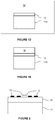
- the invention proposes a method for healing the defects of the transferred layer, in which the transferred layer (and possibly the whole of the receiving substrate which supports it) is exposed to a medium M containing lithium ions (cf. figure 1D ).
- This exposure has the effect of migrating lithium ions from the medium M towards the transferred layer 10, thus enriching the transferred layer with lithium and restoring the structure of said layer before implantation and transfer.
- hydrogen atoms located at the location of lithium atoms can migrate to medium M.
- the medium M can be a liquid, in which case the transferred layer is immersed in a bath of said liquid.
- the medium M is an acid solution of a lithium salt.
- Those skilled in the art also know how to use mixtures of LiNO 3 , KNO 3 and NaNO 3 solutions to better control the effectiveness of this operation.
- the medium M can be gaseous, in which case the transferred layer is placed in an enclosure containing said gas.
- the thickness of the transferred layer is less than 20 ⁇ m, preferably less than 2 ⁇ m.
- the medium M can be in solid phase, and the transferred layer 10 is exposed to said medium by depositing a layer of said medium on the layer 10 (cf. figure 1E ).
- a layer of said medium on the layer 10 (cf. figure 1E ).
- on here is meant either directly in contact with said layer 10, or through one or more layers formed of different materials, insofar as said intermediate layers do not block the migration of the element A of the layer constituting the medium M towards the layer 10.
- a better penetration of the ions of the element A in the layer 10 is made possible by one or more annealing steps.
- the deposited layer containing the element A can be removed at the end of the operation, possibly between two successive annealing steps.
- part of the thickness of the layer transferred to the receiving substrate is removed. This removal can be carried out by chemical mechanical polishing, by etching or by any other suitable technique.
- the figure 2 is a general view of a surface acoustic wave filter.
- Said filter comprises a piezoelectric layer 10 and two electrodes 12, 13 in the form of two interdigitated metal combs deposited on the surface of said piezoelectric layer.
- the piezoelectric layer rests on a support substrate 11.
- the piezoelectric layer 10 is monocrystalline, excellent crystalline quality being in fact necessary so as not to generate attenuation of the surface wave.
- the figure 3 is a principle view of a volume acoustic wave resonator.
- the resonator comprises a thin piezoelectric layer (that is to say a thickness generally less than 1 ⁇ m, preferably less than 0.2 ⁇ m) and two electrodes 12, 13 arranged on either side of said piezoelectric layer 10.
- the piezoelectric layer 10 rests on a support substrate 11.
- a Bragg mirror 14 is interposed between the electrode 13 and the substrate 11. Alternatively (not shown), this insulation could be achieved by providing a cavity between the substrate and the piezoelectric layer.
- the receiving substrate may not be optimal for the final application. It may then be advantageous to transfer the layer 10 onto a final substrate (not shown), the properties of which are chosen as a function of the intended application, by bonding it to said final substrate and by removing the receiving substrate by any suitable technique.
- said substrate forms the support substrate denoted 11 on the figure 2 ), metal electrodes 12, 13 in the form of two interdigitated combs.
- an isolation means which can be, for example, a Bragg mirror (as illustrated in the figure 3 ) or a cavity previously etched in the receiving substrate or in the final substrate if necessary.
Landscapes
- Engineering & Computer Science (AREA)
- Manufacturing & Machinery (AREA)
- Physics & Mathematics (AREA)
- Acoustics & Sound (AREA)
- Chemical & Material Sciences (AREA)
- Materials Engineering (AREA)
- Ceramic Engineering (AREA)
- Surface Acoustic Wave Elements And Circuit Networks Thereof (AREA)
- Crystals, And After-Treatments Of Crystals (AREA)
- Piezo-Electric Or Mechanical Vibrators, Or Delay Or Filter Circuits (AREA)
- Physical Vapour Deposition (AREA)
- Pharmaceuticals Containing Other Organic And Inorganic Compounds (AREA)
Claims (22)
- Heilungsverfahren von Fehlern einer Schicht (10) mit der Zusammensatzung ABO3, in der A aus wenigstens einem Element gebildet ist aus: Li, Na, K, H, Ca, Mg, Ba, Sr, Pb, La, Bi, Y, Dy, Gd, Tb, Ce, Pr, Nd, Sm, Eu, Ho, Zr, Sc, Ag, TI und B aus wenigstens einem Element gebildet ist aus: Nb, Ta, Sb, Ti, Zr, Sn, Ru, Fe, V, Sc, C, Ga, Al, Si, Mn, Zr, TI, wobei die genannte Schicht (10) durch ein Schichtübertragungsverfahren erhalten wird, in der ionische Arten in ein Substrat (100) mit der Zusammensetzung ABO3 derart implantiert werden, dass ein Schwächungsbereich geformt wird, der die genannte Schicht begrenzt, dann wird das genannte Substrat entlang dem Schwächungsbereich abgelöst, um eine Schicht (10) zu erhalten, die von dem Rest des Spendersubstrats abgelöst ist, dadurch gekennzeichnet, dass sie das Kontaktieren der genannten Schicht (10) mit einem Milieu (M) umfasst, das Ionen einen Bestanteils A derart enthält, dass die genannten Ionen in die genannte übertragene Schicht zum Eindringen gebracht werden.
- Verfahren gemäß Anspruch 1, bei dem die genannten Ionen in die Schicht (10) durch einen Ionenaustausch-Mechanismus eindringen.
- Verfahren gemäß einem der Ansprüche 1 oder 2, bei dem das Milieu (M), das die Ionen enthält, eine Flüssigkeit ist und die Schicht (10) in ein Bad der genannten Flüssigkeit eingetaucht ist.
- Verfahren gemäß einem der Ansprüche 1 bis 3, bei dem die Schicht (10) mit der Zusammensetzung ABO3 in ein Bad eingetaucht ist, das eine saure Lösung eines Salzes umfasst, das den genannten Bestandteil A umfasst.
- Verfahren gemäß einem der Ansprüche 1 oder 2, bei dem das Milieu (M), das die Ionen enthält, in der gashaltigen Phase ist und die Schicht (10) mit dem genannten Gas in Kontakt ist.
- Verfahren gemäß einem der Ansprüche 1 oder 2, bei dem das Milieu (M), das die Ionen enthält, in der festen Phase ist und wobei eine Schicht des genannten Milieus (M) auf der Schicht (10) aufgebracht ist.
- Verfahren gemäß Anspruch 6, umfassend wenigstens einen Temperschritt zum Begünstigen der Verbreitung des Bestandteils A des Milieus (M) zur Schicht (10).
- Verfahren gemäß einem der Ansprüche 1 bis 7, bei dem A Lithium ist.
- Verfahren gemäß Anspruch 8, bei dem die Lithiumionen durch einen umgekehrten Protonenaustausch-Mechanismus in die Schicht (10) eindringen.
- Verfahren gemäß einem der Ansprüche 8 oder 9, bei dem die Schicht (10) in ein Bad getaucht ist, das eine saure Lösung eines Lithiumsalzes umfasst.
- Verfahren gemäß einem der Ansprüche 1 bis 10, bei dem die Schicht (10) monokristallin ist.
- Herstellungsverfahren einer Schicht (10) mit einer Zusammensetzung ABO3, in der A aus wenigstens einem der Elemente gebildet ist aus: Li, Na, K, H, Ca, Mg, Ba, Sr, Pb, La, Bi, Y, Dy, Gd, Tb, Ce, Pr, Nd, Sm, Eu, Ho, Zr, Sc, Ag, TI und B aus wenigstens einem Element gebildet ist aus: Nb, Ta, Sb, Ti, Zr, Sn, Ru, Fe, V, Sc, C, Ga, Al, Si, Mn, Zr, TI, dadurch gekennzeichnet, dass es umfasst:- die Lieferung eines Spendersubstrats (100) mit der Zusammensetzung ABO3,- die Bildung eines Schwächungsbereichs (101) per Implantieren von ionischen Arten in das Spendersubstrat (100) derart, dass die Schicht (10) begrenzt wird,- das Ablösen des Spendersubstrats (100) entlang dem Schwächungsbereich (101) derart, dass die Schicht (10) erhalten wird, die vom Rest des Spendersubstrats (100) abgelöst ist, wobei die genannte Schicht Fehler umfasst,- das Umsetzen des Heilungsverfahrens der Fehler der Schicht (10) gemäß einem der Ansprüche 1 bis 11.
- Verfahren gemäß Anspruch 12, bei dem die implantierten Arten Wasserstoff und / oder Helium umfassen.
- Verfahren gemäß einem der Ansprüche 12 oder 13, bei dem vor dem Heilungsschritt ein Teil der Dicke der Schicht (10) entfernt wird.
- Verfahren gemäß einem der Ansprüche 12 bis 14, bei dem die Dicke der Schicht (10) größer ist als 2 µm, bevorzugt größer als 20 µm, wobei die genannte Schicht nach dem Ablösen des Spendersubstrats (100) selbstgetragen ist.
- Verfahren gemäß einem der Ansprüche 12 bis 14, umfassend zwischen dem Bildungsschritt des Schwächungsbereichs und dem Ablöseschritt des Spendersubstrats entlang dem Schwächungsbereich die Anwendung eines Empfängersubstrats (110) auf dem Spendersubstrat (100), wobei die Schicht (100) an der Schnittstelle zwischen den genannten Substraten (100, 110) ist, wobei die genannte Schicht (10) nach dem Ablösen des Spendersubstrats (100) auf das Empfängersubstrat (110) übertragen wird.
- Verfahren gemäß Anspruch 16, bei dem die Anwendung des Empfängersubstrats das Aufbringen des genannten Substrats (110) auf das Spendersubstrat (100) umfasst.
- Verfahren gemäß Anspruch 16, bei dem die Anwendung des Empfängersubstrats das Verkleben des genannten Substrats (110) auf dem Spendersubstrat (100) umfasst.
- Verfahren gemäß einem der Ansprüche 16 bis 18, bei dem die Dicke der Schicht (10) geringer ist als 20 µm.
- Verfahren gemäß einem der Ansprüche 16 bis 19, bei dem wenigstens eine elektrisch isolierende Schicht und / oder wenigstens eine elektrisch leitende Schicht an der Schnittstelle zwischen dem Empfängersubstrat (110) und der zu übertragenden Schicht (10) geformt wird.
- Herstellungsverfahren einer Vorrichtung mit akustischen Volumenwellen, umfassend die Bildung von Elektroden (12, 13) auf zwei Hauptseiten gegenüber einer piezoelektrischen Schicht (10), dadurch gekennzeichnet, dass sie die Herstellung der genannten piezoelektrischen Schicht (10) durch ein Verfahren gemäß einem der Ansprüche 12 bis 20 umfasst.
- Herstellungsverfahren einer Vorrichtung mit akustischen Oberflächenwellen, umfassend das Bilden von zwei Elektroden (12, 13), die auf der Oberfläche einer piezoelektrischen Schicht (10) versetzt angeordnet sind, dadurch gekennzeichnet, dass es die Herstellung der genannten piezoelektrischen Schicht durch ein Verfahren gemäß einem der Ansprüche 12 bis 20 umfasst.
Applications Claiming Priority (2)
| Application Number | Priority Date | Filing Date | Title |
|---|---|---|---|
| FR1654673A FR3051979B1 (fr) | 2016-05-25 | 2016-05-25 | Procede de guerison de defauts dans une couche obtenue par implantation puis detachement d'un substrat |
| PCT/FR2017/051290 WO2017203173A1 (fr) | 2016-05-25 | 2017-05-24 | Procede de guerison de defauts dans une couche obtenue par implantation puis detachement d'un substrat |
Publications (2)
| Publication Number | Publication Date |
|---|---|
| EP3465787A1 EP3465787A1 (de) | 2019-04-10 |
| EP3465787B1 true EP3465787B1 (de) | 2020-03-18 |
Family
ID=56557781
Family Applications (1)
| Application Number | Title | Priority Date | Filing Date |
|---|---|---|---|
| EP17732503.2A Active EP3465787B1 (de) | 2016-05-25 | 2017-05-24 | Verfahren zur reparatur von defekten in einer schicht durch implantation und dann ablösung von einem substrat |
Country Status (8)
| Country | Link |
|---|---|
| US (1) | US11398595B2 (de) |
| EP (1) | EP3465787B1 (de) |
| JP (1) | JP7066638B2 (de) |
| KR (1) | KR102232158B1 (de) |
| CN (1) | CN109155358B (de) |
| FR (1) | FR3051979B1 (de) |
| SG (1) | SG11201810356VA (de) |
| WO (1) | WO2017203173A1 (de) |
Cited By (1)
| Publication number | Priority date | Publication date | Assignee | Title |
|---|---|---|---|---|
| EP3525347A4 (de) * | 2016-10-06 | 2020-09-23 | Shin-Etsu Chemical Co., Ltd. | Verbundsubstrat und verfahren zur herstellung des verbundsubstrats |
Family Cites Families (25)
| Publication number | Priority date | Publication date | Assignee | Title |
|---|---|---|---|---|
| US6786967B1 (en) * | 1998-05-11 | 2004-09-07 | California Institute Of Technology | Ion exchange waveguides and methods of fabrication |
| US7548015B2 (en) * | 2000-11-02 | 2009-06-16 | Danfoss A/S | Multilayer composite and a method of making such |
| FR2816445B1 (fr) * | 2000-11-06 | 2003-07-25 | Commissariat Energie Atomique | Procede de fabrication d'une structure empilee comprenant une couche mince adherant a un substrat cible |
| EP1271221A1 (de) * | 2001-06-28 | 2003-01-02 | Corning O.T.I. S.p.A. | Integrierter optischer Wellenleiter |
| US20030127042A1 (en) * | 2002-01-09 | 2003-07-10 | Der-Hou Tsou | Method of forming high quality waveguides by vapor-phase proton-exchange process with post-thermal annealing and reversed proton-exchange |
| FR2855909B1 (fr) * | 2003-06-06 | 2005-08-26 | Soitec Silicon On Insulator | Procede d'obtention concomitante d'au moins une paire de structures comprenant au moins une couche utile reportee sur un substrat |
| KR100596391B1 (ko) * | 2004-12-03 | 2006-07-04 | 한국전자통신연구원 | 강유전체/상유전체 다층 박막 및 그 제조 방법과 그를이용한 초고주파 가변 소자 |
| US7566629B2 (en) * | 2005-06-16 | 2009-07-28 | International Business Machines Corporation | Patterned silicon-on-insulator layers and methods for forming the same |
| FR2896255B1 (fr) * | 2006-01-17 | 2008-05-09 | Soitec Silicon On Insulator | Procede d'ajustement de la contrainte d'un substrat en un materiau semi-conducteur |
| WO2009081651A1 (ja) | 2007-12-25 | 2009-07-02 | Murata Manufacturing Co., Ltd. | 複合圧電基板の製造方法 |
| FR2930072B1 (fr) * | 2008-04-15 | 2010-08-20 | Commissariat Energie Atomique | Procede de transfert d'une couche mince par echange protonique. |
| EP2161741B1 (de) * | 2008-09-03 | 2014-06-11 | Soitec | Verfahren zur Herstellung eines Halbleiters auf einem Isoliersubstrat mit verringerter SECCO-Fehlerdichte |
| JP4582235B2 (ja) * | 2008-10-31 | 2010-11-17 | 株式会社村田製作所 | 圧電デバイスの製造方法 |
| JP4821834B2 (ja) * | 2008-10-31 | 2011-11-24 | 株式会社村田製作所 | 圧電性複合基板の製造方法 |
| US8189981B2 (en) | 2009-11-23 | 2012-05-29 | The Aerospace Corporation | Stable lithium niobate waveguides, and methods of making and using same |
| JP5569537B2 (ja) | 2009-11-26 | 2014-08-13 | 株式会社村田製作所 | 圧電デバイスの製造方法 |
| FR2972564B1 (fr) * | 2011-03-08 | 2016-11-04 | S O I Tec Silicon On Insulator Tech | Procédé de traitement d'une structure de type semi-conducteur sur isolant |
| FR2977260B1 (fr) * | 2011-06-30 | 2013-07-19 | Soitec Silicon On Insulator | Procede de fabrication d'une couche epitaxiale epaisse de nitrure de gallium sur un substrat de silicium ou analogue et couche obtenue par ledit procede |
| FR2983342B1 (fr) * | 2011-11-30 | 2016-05-20 | Soitec Silicon On Insulator | Procede de fabrication d'une heterostructure limitant la formation de defauts et heterostructure ainsi obtenue |
| EP2828901B1 (de) * | 2012-03-21 | 2017-01-04 | Parker Hannifin Corporation | Rolle-an-rolle-herstellungsverfahren zur herstellung selbstheilender elektroaktiver polymervorrichtungen |
| JP6265915B2 (ja) * | 2012-12-26 | 2018-01-24 | 日本碍子株式会社 | 複合基板の製法 |
| US10095057B2 (en) * | 2013-10-23 | 2018-10-09 | Honeywell International Inc. | Treatment and/or stabilizing gases in an optical gyro based on an inorganic waveguide |
| WO2016118536A2 (en) * | 2015-01-20 | 2016-07-28 | The Johns Hopkins University | Printable high dielectric constant and self-healable dielectric polymer composition |
| CN104852271A (zh) * | 2015-05-29 | 2015-08-19 | 南京信息工程大学 | 一种波导激光器的制备方法 |
| JP6728630B2 (ja) * | 2015-10-29 | 2020-07-22 | セイコーエプソン株式会社 | 圧電素子、圧電モジュール、電子機器、及び圧電素子の製造方法 |
-
2016
- 2016-05-25 FR FR1654673A patent/FR3051979B1/fr not_active Expired - Fee Related
-
2017
- 2017-05-24 US US16/304,071 patent/US11398595B2/en active Active
- 2017-05-24 CN CN201780032137.7A patent/CN109155358B/zh active Active
- 2017-05-24 JP JP2018561713A patent/JP7066638B2/ja active Active
- 2017-05-24 KR KR1020187037414A patent/KR102232158B1/ko active Active
- 2017-05-24 EP EP17732503.2A patent/EP3465787B1/de active Active
- 2017-05-24 WO PCT/FR2017/051290 patent/WO2017203173A1/fr not_active Ceased
- 2017-05-24 SG SG11201810356VA patent/SG11201810356VA/en unknown
Non-Patent Citations (1)
| Title |
|---|
| None * |
Cited By (1)
| Publication number | Priority date | Publication date | Assignee | Title |
|---|---|---|---|---|
| EP3525347A4 (de) * | 2016-10-06 | 2020-09-23 | Shin-Etsu Chemical Co., Ltd. | Verbundsubstrat und verfahren zur herstellung des verbundsubstrats |
Also Published As
| Publication number | Publication date |
|---|---|
| JP2019519154A (ja) | 2019-07-04 |
| CN109155358B (zh) | 2022-06-03 |
| CN109155358A (zh) | 2019-01-04 |
| FR3051979A1 (fr) | 2017-12-01 |
| JP7066638B2 (ja) | 2022-05-13 |
| KR102232158B1 (ko) | 2021-03-25 |
| EP3465787A1 (de) | 2019-04-10 |
| FR3051979B1 (fr) | 2018-05-18 |
| SG11201810356VA (en) | 2018-12-28 |
| KR20190013896A (ko) | 2019-02-11 |
| WO2017203173A1 (fr) | 2017-11-30 |
| US20200328342A1 (en) | 2020-10-15 |
| US11398595B2 (en) | 2022-07-26 |
Similar Documents
| Publication | Publication Date | Title |
|---|---|---|
| EP2628243B1 (de) | Heterogene akustische struktur aus einem homogenen material | |
| FR3045677B1 (fr) | Procede de fabrication d'une couche monocristalline, notamment piezoelectrique | |
| EP4006998B1 (de) | Verfahren zur herstellung eines bauteils mit einer schicht aus monokristallinem material, das mit hohen wärmehaushalten kompatibel ist | |
| EP3706180B1 (de) | Verfahren zur herstellung eines mikroelektromechanischen systems, das aus einer abgeschiedenen piezoelektrischen oder ferroelektrischen schicht hergestellt wird | |
| EP2591515B1 (de) | Verfahren zur implantierung eines piezoelektrischen materials | |
| EP3394908B1 (de) | Substrat für eine temperaturkompensierte oberflächenschallwellenvorrichtung oder volumenschallwellenvorrichtung | |
| FR3045678A1 (fr) | Procede de fabrication d'une couche piezoelectrique monocristalline et dispositif microelectronique, photonique ou optique comprenant une telle couche | |
| EP3465787B1 (de) | Verfahren zur reparatur von defekten in einer schicht durch implantation und dann ablösung von einem substrat | |
| EP3766094B1 (de) | Verfahren zur herstellung einer dünnschicht aus einem ferroelektrikum auf alkalibasis | |
| EP3465788B1 (de) | Verfahren zur herstellung einer schicht | |
| FR3141308A1 (fr) | Procede de fabrication d’une couche piezoelectrique sur un substrat |
Legal Events
| Date | Code | Title | Description |
|---|---|---|---|
| STAA | Information on the status of an ep patent application or granted ep patent |
Free format text: STATUS: UNKNOWN |
|
| STAA | Information on the status of an ep patent application or granted ep patent |
Free format text: STATUS: THE INTERNATIONAL PUBLICATION HAS BEEN MADE |
|
| PUAI | Public reference made under article 153(3) epc to a published international application that has entered the european phase |
Free format text: ORIGINAL CODE: 0009012 |
|
| STAA | Information on the status of an ep patent application or granted ep patent |
Free format text: STATUS: REQUEST FOR EXAMINATION WAS MADE |
|
| 17P | Request for examination filed |
Effective date: 20181217 |
|
| AK | Designated contracting states |
Kind code of ref document: A1 Designated state(s): AL AT BE BG CH CY CZ DE DK EE ES FI FR GB GR HR HU IE IS IT LI LT LU LV MC MK MT NL NO PL PT RO RS SE SI SK SM TR |
|
| AX | Request for extension of the european patent |
Extension state: BA ME |
|
| DAV | Request for validation of the european patent (deleted) | ||
| DAX | Request for extension of the european patent (deleted) | ||
| GRAP | Despatch of communication of intention to grant a patent |
Free format text: ORIGINAL CODE: EPIDOSNIGR1 |
|
| STAA | Information on the status of an ep patent application or granted ep patent |
Free format text: STATUS: GRANT OF PATENT IS INTENDED |
|
| INTG | Intention to grant announced |
Effective date: 20191104 |
|
| GRAS | Grant fee paid |
Free format text: ORIGINAL CODE: EPIDOSNIGR3 |
|
| GRAA | (expected) grant |
Free format text: ORIGINAL CODE: 0009210 |
|
| STAA | Information on the status of an ep patent application or granted ep patent |
Free format text: STATUS: THE PATENT HAS BEEN GRANTED |
|
| AK | Designated contracting states |
Kind code of ref document: B1 Designated state(s): AL AT BE BG CH CY CZ DE DK EE ES FI FR GB GR HR HU IE IS IT LI LT LU LV MC MK MT NL NO PL PT RO RS SE SI SK SM TR |
|
| REG | Reference to a national code |
Ref country code: GB Ref legal event code: FG4D Free format text: NOT ENGLISH |
|
| REG | Reference to a national code |
Ref country code: DE Ref legal event code: R096 Ref document number: 602017013339 Country of ref document: DE |
|
| REG | Reference to a national code |
Ref country code: AT Ref legal event code: REF Ref document number: 1246946 Country of ref document: AT Kind code of ref document: T Effective date: 20200415 Ref country code: IE Ref legal event code: FG4D Free format text: LANGUAGE OF EP DOCUMENT: FRENCH |
|
| REG | Reference to a national code |
Ref country code: CH Ref legal event code: NV Representative=s name: MICHELI AND CIE SA, CH |
|
| REG | Reference to a national code |
Ref country code: FI Ref legal event code: FGE |
|
| PG25 | Lapsed in a contracting state [announced via postgrant information from national office to epo] |
Ref country code: RS Free format text: LAPSE BECAUSE OF FAILURE TO SUBMIT A TRANSLATION OF THE DESCRIPTION OR TO PAY THE FEE WITHIN THE PRESCRIBED TIME-LIMIT Effective date: 20200318 Ref country code: NO Free format text: LAPSE BECAUSE OF FAILURE TO SUBMIT A TRANSLATION OF THE DESCRIPTION OR TO PAY THE FEE WITHIN THE PRESCRIBED TIME-LIMIT Effective date: 20200618 |
|
| REG | Reference to a national code |
Ref country code: NL Ref legal event code: MP Effective date: 20200318 |
|
| PG25 | Lapsed in a contracting state [announced via postgrant information from national office to epo] |
Ref country code: HR Free format text: LAPSE BECAUSE OF FAILURE TO SUBMIT A TRANSLATION OF THE DESCRIPTION OR TO PAY THE FEE WITHIN THE PRESCRIBED TIME-LIMIT Effective date: 20200318 Ref country code: BG Free format text: LAPSE BECAUSE OF FAILURE TO SUBMIT A TRANSLATION OF THE DESCRIPTION OR TO PAY THE FEE WITHIN THE PRESCRIBED TIME-LIMIT Effective date: 20200618 Ref country code: SE Free format text: LAPSE BECAUSE OF FAILURE TO SUBMIT A TRANSLATION OF THE DESCRIPTION OR TO PAY THE FEE WITHIN THE PRESCRIBED TIME-LIMIT Effective date: 20200318 Ref country code: LV Free format text: LAPSE BECAUSE OF FAILURE TO SUBMIT A TRANSLATION OF THE DESCRIPTION OR TO PAY THE FEE WITHIN THE PRESCRIBED TIME-LIMIT Effective date: 20200318 Ref country code: GR Free format text: LAPSE BECAUSE OF FAILURE TO SUBMIT A TRANSLATION OF THE DESCRIPTION OR TO PAY THE FEE WITHIN THE PRESCRIBED TIME-LIMIT Effective date: 20200619 |
|
| REG | Reference to a national code |
Ref country code: LT Ref legal event code: MG4D |
|
| PG25 | Lapsed in a contracting state [announced via postgrant information from national office to epo] |
Ref country code: NL Free format text: LAPSE BECAUSE OF FAILURE TO SUBMIT A TRANSLATION OF THE DESCRIPTION OR TO PAY THE FEE WITHIN THE PRESCRIBED TIME-LIMIT Effective date: 20200318 |
|
| PG25 | Lapsed in a contracting state [announced via postgrant information from national office to epo] |
Ref country code: IS Free format text: LAPSE BECAUSE OF FAILURE TO SUBMIT A TRANSLATION OF THE DESCRIPTION OR TO PAY THE FEE WITHIN THE PRESCRIBED TIME-LIMIT Effective date: 20200718 Ref country code: CZ Free format text: LAPSE BECAUSE OF FAILURE TO SUBMIT A TRANSLATION OF THE DESCRIPTION OR TO PAY THE FEE WITHIN THE PRESCRIBED TIME-LIMIT Effective date: 20200318 Ref country code: SK Free format text: LAPSE BECAUSE OF FAILURE TO SUBMIT A TRANSLATION OF THE DESCRIPTION OR TO PAY THE FEE WITHIN THE PRESCRIBED TIME-LIMIT Effective date: 20200318 Ref country code: RO Free format text: LAPSE BECAUSE OF FAILURE TO SUBMIT A TRANSLATION OF THE DESCRIPTION OR TO PAY THE FEE WITHIN THE PRESCRIBED TIME-LIMIT Effective date: 20200318 Ref country code: SM Free format text: LAPSE BECAUSE OF FAILURE TO SUBMIT A TRANSLATION OF THE DESCRIPTION OR TO PAY THE FEE WITHIN THE PRESCRIBED TIME-LIMIT Effective date: 20200318 Ref country code: PT Free format text: LAPSE BECAUSE OF FAILURE TO SUBMIT A TRANSLATION OF THE DESCRIPTION OR TO PAY THE FEE WITHIN THE PRESCRIBED TIME-LIMIT Effective date: 20200812 Ref country code: EE Free format text: LAPSE BECAUSE OF FAILURE TO SUBMIT A TRANSLATION OF THE DESCRIPTION OR TO PAY THE FEE WITHIN THE PRESCRIBED TIME-LIMIT Effective date: 20200318 Ref country code: LT Free format text: LAPSE BECAUSE OF FAILURE TO SUBMIT A TRANSLATION OF THE DESCRIPTION OR TO PAY THE FEE WITHIN THE PRESCRIBED TIME-LIMIT Effective date: 20200318 |
|
| REG | Reference to a national code |
Ref country code: AT Ref legal event code: MK05 Ref document number: 1246946 Country of ref document: AT Kind code of ref document: T Effective date: 20200318 |
|
| REG | Reference to a national code |
Ref country code: DE Ref legal event code: R097 Ref document number: 602017013339 Country of ref document: DE |
|
| PLBE | No opposition filed within time limit |
Free format text: ORIGINAL CODE: 0009261 |
|
| STAA | Information on the status of an ep patent application or granted ep patent |
Free format text: STATUS: NO OPPOSITION FILED WITHIN TIME LIMIT |
|
| PG25 | Lapsed in a contracting state [announced via postgrant information from national office to epo] |
Ref country code: AT Free format text: LAPSE BECAUSE OF FAILURE TO SUBMIT A TRANSLATION OF THE DESCRIPTION OR TO PAY THE FEE WITHIN THE PRESCRIBED TIME-LIMIT Effective date: 20200318 Ref country code: DK Free format text: LAPSE BECAUSE OF FAILURE TO SUBMIT A TRANSLATION OF THE DESCRIPTION OR TO PAY THE FEE WITHIN THE PRESCRIBED TIME-LIMIT Effective date: 20200318 Ref country code: MC Free format text: LAPSE BECAUSE OF FAILURE TO SUBMIT A TRANSLATION OF THE DESCRIPTION OR TO PAY THE FEE WITHIN THE PRESCRIBED TIME-LIMIT Effective date: 20200318 Ref country code: ES Free format text: LAPSE BECAUSE OF FAILURE TO SUBMIT A TRANSLATION OF THE DESCRIPTION OR TO PAY THE FEE WITHIN THE PRESCRIBED TIME-LIMIT Effective date: 20200318 |
|
| 26N | No opposition filed |
Effective date: 20201221 |
|
| PG25 | Lapsed in a contracting state [announced via postgrant information from national office to epo] |
Ref country code: PL Free format text: LAPSE BECAUSE OF FAILURE TO SUBMIT A TRANSLATION OF THE DESCRIPTION OR TO PAY THE FEE WITHIN THE PRESCRIBED TIME-LIMIT Effective date: 20200318 |
|
| PG25 | Lapsed in a contracting state [announced via postgrant information from national office to epo] |
Ref country code: LU Free format text: LAPSE BECAUSE OF NON-PAYMENT OF DUE FEES Effective date: 20200524 |
|
| PG25 | Lapsed in a contracting state [announced via postgrant information from national office to epo] |
Ref country code: IE Free format text: LAPSE BECAUSE OF NON-PAYMENT OF DUE FEES Effective date: 20200524 |
|
| PG25 | Lapsed in a contracting state [announced via postgrant information from national office to epo] |
Ref country code: SI Free format text: LAPSE BECAUSE OF FAILURE TO SUBMIT A TRANSLATION OF THE DESCRIPTION OR TO PAY THE FEE WITHIN THE PRESCRIBED TIME-LIMIT Effective date: 20200318 |
|
| PG25 | Lapsed in a contracting state [announced via postgrant information from national office to epo] |
Ref country code: TR Free format text: LAPSE BECAUSE OF FAILURE TO SUBMIT A TRANSLATION OF THE DESCRIPTION OR TO PAY THE FEE WITHIN THE PRESCRIBED TIME-LIMIT Effective date: 20200318 Ref country code: MT Free format text: LAPSE BECAUSE OF FAILURE TO SUBMIT A TRANSLATION OF THE DESCRIPTION OR TO PAY THE FEE WITHIN THE PRESCRIBED TIME-LIMIT Effective date: 20200318 Ref country code: CY Free format text: LAPSE BECAUSE OF FAILURE TO SUBMIT A TRANSLATION OF THE DESCRIPTION OR TO PAY THE FEE WITHIN THE PRESCRIBED TIME-LIMIT Effective date: 20200318 |
|
| PG25 | Lapsed in a contracting state [announced via postgrant information from national office to epo] |
Ref country code: MK Free format text: LAPSE BECAUSE OF FAILURE TO SUBMIT A TRANSLATION OF THE DESCRIPTION OR TO PAY THE FEE WITHIN THE PRESCRIBED TIME-LIMIT Effective date: 20200318 Ref country code: AL Free format text: LAPSE BECAUSE OF FAILURE TO SUBMIT A TRANSLATION OF THE DESCRIPTION OR TO PAY THE FEE WITHIN THE PRESCRIBED TIME-LIMIT Effective date: 20200318 |
|
| REG | Reference to a national code |
Ref country code: DE Ref legal event code: R079 Ref document number: 602017013339 Country of ref document: DE Free format text: PREVIOUS MAIN CLASS: H01L0041312000 Ipc: H10N0030072000 |
|
| PGFP | Annual fee paid to national office [announced via postgrant information from national office to epo] |
Ref country code: FI Payment date: 20250513 Year of fee payment: 9 |
|
| PGFP | Annual fee paid to national office [announced via postgrant information from national office to epo] |
Ref country code: DE Payment date: 20250402 Year of fee payment: 9 |
|
| PGFP | Annual fee paid to national office [announced via postgrant information from national office to epo] |
Ref country code: IT Payment date: 20250422 Year of fee payment: 9 Ref country code: BE Payment date: 20250410 Year of fee payment: 9 |
|
| PGFP | Annual fee paid to national office [announced via postgrant information from national office to epo] |
Ref country code: FR Payment date: 20250422 Year of fee payment: 9 |
|
| PGFP | Annual fee paid to national office [announced via postgrant information from national office to epo] |
Ref country code: CH Payment date: 20250601 Year of fee payment: 9 |
|
| PGFP | Annual fee paid to national office [announced via postgrant information from national office to epo] |
Ref country code: GB Payment date: 20260312 Year of fee payment: 10 |