EP3470860A1 - Circuit de détection et de détermination de tension, et système de batterie d'alimentation le comprenant - Google Patents
Circuit de détection et de détermination de tension, et système de batterie d'alimentation le comprenant Download PDFInfo
- Publication number
- EP3470860A1 EP3470860A1 EP17809632.7A EP17809632A EP3470860A1 EP 3470860 A1 EP3470860 A1 EP 3470860A1 EP 17809632 A EP17809632 A EP 17809632A EP 3470860 A1 EP3470860 A1 EP 3470860A1
- Authority
- EP
- European Patent Office
- Prior art keywords
- detection
- voltage
- processing module
- pmos transistor
- resistor
- Prior art date
- Legal status (The legal status is an assumption and is not a legal conclusion. Google has not performed a legal analysis and makes no representation as to the accuracy of the status listed.)
- Withdrawn
Links
- 238000001514 detection method Methods 0.000 title claims abstract description 161
- 238000012545 processing Methods 0.000 claims abstract description 127
- 238000005070 sampling Methods 0.000 claims abstract description 40
- 238000009966 trimming Methods 0.000 claims description 36
- 238000007599 discharging Methods 0.000 abstract description 16
- 238000000034 method Methods 0.000 description 10
- 238000010586 diagram Methods 0.000 description 8
- LIDGFHXPUOJZMK-UHFFFAOYSA-N 2,6-dimethyl-1-oxidopyridin-1-ium Chemical compound CC1=CC=CC(C)=[N+]1[O-] LIDGFHXPUOJZMK-UHFFFAOYSA-N 0.000 description 5
- 238000012360 testing method Methods 0.000 description 5
- 230000008569 process Effects 0.000 description 3
- 238000005516 engineering process Methods 0.000 description 2
- 230000002411 adverse Effects 0.000 description 1
- 238000004891 communication Methods 0.000 description 1
- 238000013461 design Methods 0.000 description 1
- 238000004880 explosion Methods 0.000 description 1
- 230000006872 improvement Effects 0.000 description 1
- 238000009434 installation Methods 0.000 description 1
- 230000003993 interaction Effects 0.000 description 1
- 230000004048 modification Effects 0.000 description 1
- 238000012986 modification Methods 0.000 description 1
Images

Classifications
-
- G—PHYSICS
- G01—MEASURING; TESTING
- G01R—MEASURING ELECTRIC VARIABLES; MEASURING MAGNETIC VARIABLES
- G01R19/00—Arrangements for measuring currents or voltages or for indicating presence or sign thereof
- G01R19/165—Indicating that current or voltage is either above or below a predetermined value or within or outside a predetermined range of values
- G01R19/16504—Indicating that current or voltage is either above or below a predetermined value or within or outside a predetermined range of values characterised by the components employed
- G01R19/16519—Indicating that current or voltage is either above or below a predetermined value or within or outside a predetermined range of values characterised by the components employed using FET's
-
- G—PHYSICS
- G01—MEASURING; TESTING
- G01R—MEASURING ELECTRIC VARIABLES; MEASURING MAGNETIC VARIABLES
- G01R31/00—Arrangements for testing electric properties; Arrangements for locating electric faults; Arrangements for electrical testing characterised by what is being tested not provided for elsewhere
- G01R31/36—Arrangements for testing, measuring or monitoring the electrical condition of accumulators or electric batteries, e.g. capacity or state of charge [SoC]
- G01R31/396—Acquisition or processing of data for testing or for monitoring individual cells or groups of cells within a battery
-
- G—PHYSICS
- G01—MEASURING; TESTING
- G01R—MEASURING ELECTRIC VARIABLES; MEASURING MAGNETIC VARIABLES
- G01R19/00—Arrangements for measuring currents or voltages or for indicating presence or sign thereof
- G01R19/165—Indicating that current or voltage is either above or below a predetermined value or within or outside a predetermined range of values
- G01R19/16533—Indicating that current or voltage is either above or below a predetermined value or within or outside a predetermined range of values characterised by the application
- G01R19/16538—Indicating that current or voltage is either above or below a predetermined value or within or outside a predetermined range of values characterised by the application in AC or DC supplies
- G01R19/16542—Indicating that current or voltage is either above or below a predetermined value or within or outside a predetermined range of values characterised by the application in AC or DC supplies for batteries
-
- G—PHYSICS
- G01—MEASURING; TESTING
- G01R—MEASURING ELECTRIC VARIABLES; MEASURING MAGNETIC VARIABLES
- G01R19/00—Arrangements for measuring currents or voltages or for indicating presence or sign thereof
- G01R19/165—Indicating that current or voltage is either above or below a predetermined value or within or outside a predetermined range of values
-
- G—PHYSICS
- G01—MEASURING; TESTING
- G01R—MEASURING ELECTRIC VARIABLES; MEASURING MAGNETIC VARIABLES
- G01R31/00—Arrangements for testing electric properties; Arrangements for locating electric faults; Arrangements for electrical testing characterised by what is being tested not provided for elsewhere
- G01R31/36—Arrangements for testing, measuring or monitoring the electrical condition of accumulators or electric batteries, e.g. capacity or state of charge [SoC]
-
- G—PHYSICS
- G01—MEASURING; TESTING
- G01R—MEASURING ELECTRIC VARIABLES; MEASURING MAGNETIC VARIABLES
- G01R31/00—Arrangements for testing electric properties; Arrangements for locating electric faults; Arrangements for electrical testing characterised by what is being tested not provided for elsewhere
- G01R31/36—Arrangements for testing, measuring or monitoring the electrical condition of accumulators or electric batteries, e.g. capacity or state of charge [SoC]
- G01R31/382—Arrangements for monitoring battery or accumulator variables, e.g. SoC
- G01R31/3835—Arrangements for monitoring battery or accumulator variables, e.g. SoC involving only voltage measurements
-
- G—PHYSICS
- G01—MEASURING; TESTING
- G01R—MEASURING ELECTRIC VARIABLES; MEASURING MAGNETIC VARIABLES
- G01R31/00—Arrangements for testing electric properties; Arrangements for locating electric faults; Arrangements for electrical testing characterised by what is being tested not provided for elsewhere
- G01R31/36—Arrangements for testing, measuring or monitoring the electrical condition of accumulators or electric batteries, e.g. capacity or state of charge [SoC]
- G01R31/382—Arrangements for monitoring battery or accumulator variables, e.g. SoC
- G01R31/3842—Arrangements for monitoring battery or accumulator variables, e.g. SoC combining voltage and current measurements
-
- G—PHYSICS
- G01—MEASURING; TESTING
- G01R—MEASURING ELECTRIC VARIABLES; MEASURING MAGNETIC VARIABLES
- G01R19/00—Arrangements for measuring currents or voltages or for indicating presence or sign thereof
- G01R19/14—Indicating direction of current; Indicating polarity of voltage
Definitions
- the present invention relates to the field of power supply technologies, and in particular, to a voltage detection and determination circuit and a power battery system having the same.
- a battery During application of a battery pack, a battery generally has three states, a charging state, a standing state, and a discharging state. To correctly protect the battery pack in different environments in a timely manner, the charging and discharging states of the battery pack always need to be identified. Especially when the battery pack needs temperature protection, there is a significant difference between a charging protection temperature and a discharging protection temperature. If the charging and discharging states are incorrectly identified, different temperatures may cause damage to the battery pack, and even have explosion hazards. Therefore, accurate identification of the charging and discharging states of the battery pack is crucial.
- an objective of the present invention is to provide a voltage detection and determination circuit.
- the circuit does not need a reference voltage, and has a simple circuit structure. Moreover, there is no need to consider an influence caused by an offset voltage of a comparator. A voltage sampled by a sampling end may be accurately detected and determined, so that charging and discharging states of a battery pack are correctly identified.
- Another objective of the present invention is to provide a power battery system.
- an embodiment of an aspect of the present invention provides a voltage detection and determination circuit, including: a detection processing module, where the detection processing module is connected to a voltage sampling end, and the detection processing module is configured to output a first detection voltage based on a voltage sampled by the voltage sampling end; a detection similarity processing module, where the detection similarity processing module is used to imitate the detection processing module, to generate a reference voltage corresponding to the first detection voltage; a current source module, where the current source module is connected to the detection processing module and the detection similarity processing module, and the current source module provides a bias current to the detection processing module and the detection similarity processing module; and a comparison processing module, where the comparison processing module is connected to the detection processing module and the detection similarity processing module, and the comparison processing module performs comparison processing on the first detection voltage and the reference voltage, to output a voltage detection signal.
- the detection processing module outputs the first detection voltage based on the voltage sampled by the voltage sampling end, the detection similarity processing module imitates the detection processing module, to generate the reference voltage corresponding to the first detection voltage, then the current source module provides the bias current to the detection processing module and the detection similarity processing module, and finally the comparison processing module performs comparison processing on the first detection voltage and the reference voltage, to output the voltage detection signal.
- the circuit does not need a reference voltage, and has a simple circuit structure. Moreover, there is no need to consider an influence caused by an offset voltage of a comparator. A voltage sampled by a sampling end may be accurately detected and determined, so that charging and discharging states of a battery pack may be correctly identified.
- an embodiment of another aspect of the present invention provides a power battery system, including the foregoing voltage detection and determination circuit.
- the detection similarity processing module is used to imitate the detection processing module, to generate a reference voltage.
- a reference voltage is not needed, and a circuit structure is simple. Moreover, there is no need to consider an influence caused by an offset voltage of a comparator. A voltage sampled by a sampling end may be accurately detected and determined, so that charging and discharging states of a battery pack are correctly identified.
- charging and discharging states of a battery pack need to be identified based on a current direction.
- a common practice is to convert a current flowing through a current detection resistor Rsense into a voltage for detection. Whether a voltage V VIN of a VIN terminal of an integrated circuit (IC) is positive or negative may be determined based on a current direction.
- IC integrated circuit
- V VIN I ⁇ Rsense.
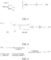
- the detected voltage V VIN of the VIN terminal is directly compared and determined. That is, one end of a comparator COMP is connected to the VIN terminal, and another end is connected to a reference voltage. Because the voltage VIN is very small, the reference voltage is usually a very small voltage VREFB that is obtained after a relatively large reference voltage VREFA is divided by using resistors. Advantages of this implementation method are: A principle is simple, and the method is easily conceived of. However, the method has many disadvantages: First, to obtain a relatively large reference voltage VREFA, a circuit needs to be added for implementation. Second, VREFB obtained through division by the resistors is affected by the voltage VREFA and ratio precision of voltage divider resistors R1 and R2.
- a determination result of VIN is affected by an offset voltage VOS of the comparator COMP.
- voltages for direct comparison are relatively small, and therefore, an input common mode level is very small, affecting a gain and an inversion speed of comparison.
- resistances of the voltage divider resistors R1 and R2 are relatively large, and a relatively wafer area is occupied. This is adverse to cost control.
- maladjustment of the comparator also cannot be ignored.
- an improvement is made based on the direct comparison shown in FIG. 3 , and the voltage V VIN of the VIN terminal is proportionally amplified by using an operational amplifier AMP and then is compared with the reference voltage.
- Advantages of this method are: After the voltage is proportionally amplified, voltages that are of two ends of the comparator COMP and that are for comparison are increased, a problem of an insufficient gain caused by a relatively low input common mode level of the comparator COMP is resolved, and voltage division does not need to be performed on the generated reference voltage, so that direct comparison may be performed, thereby reducing a resistance used by voltage division of the reference voltage and reducing a part of the wafer area.
- the present invention provides a voltage detection and determination circuit.
- the circuit does not need to generate a reference voltage, thereby reducing used circuits.
- an influence caused by an offset voltage VOS of the comparator does not need to be considered.
- FIG. 5 is a schematic block diagram of a voltage detection and determination circuit according to an embodiment of the present invention.
- the voltage detection and determination circuit includes a detection processing module 10, a detection similarity processing module 20, a current source module 30, and a comparison processing module 40.
- the detection processing module 10 is connected to a voltage sampling end VIN, and the detection processing module 10 is configured to output a first detection voltage VN based on a voltage V VIN1 sampled by the voltage sampling end VIN.
- the detection similarity processing module 20 is configured to imitate the detection processing module 10, to generate a reference voltage VP corresponding to the first detection voltage VN.
- the current source module 30 is connected to the detection processing module 10 and the detection similarity processing module 20, and the current source module 30 provides a bias current to the detection processing module 10 and the detection similarity processing module 20.
- the comparison processing module 40 is connected to the detection processing module 10 and the detection similarity processing module 20, and the comparison processing module 40 performs comparison processing on the first detection voltage VN and the reference voltage VP, to output a voltage detection signal.
- the detection processing module 10 performs level shift processing on the voltage V VIN1 sampled by the voltage sampling end VIN, to output the first detection voltage VN.
- the detection similarity processing module 20 may include a resistance trimming unit 201.
- the resistance trimming unit 201 is connected between the current source module 30 and the comparison processing module 40.
- the resistance trimming unit 201 performs resistance trimming based on resistance and current parameters of the detection similarity processing module 20 and the voltage V VIN1 sampled by the voltage sampling end VIN for the first time.
- the resistance trimming unit 201 obtains the voltage V VIN1 sampled by the voltage sampling end VIN for the first time by using the comparison processing module 40.
- the voltage sampling end VIN is connected to the detection processing module 10.
- Level shift processing is performed on the voltage V VIN1 sampled by the voltage sampling end VIN, to obtain a voltage VN having a fixed relationship with V VIN1 .
- the detection processing module 10 is connected to one end of the comparison processing module 40.
- the detection processing module 10 is imitated, to copy the detection similarity processing module 20 having a same structure as that of the detection processing module 10.
- the detection similarity processing module 20 generates the reference voltage VP, and is connected to another end of the comparison processing module 40.
- the detection similarity processing module 20 is connected to a test bench 50.
- the test bench 50 is configured to detect the resistance and current parameters of the detection similarity processing module 20.
- a detected voltage of the voltage sampling end VIN is V VIN1
- an actual resistance of the detection similarity processing module 20 tested by the test bench 50 is R X
- a theoretical value of a resistance of the detection similarity processing module 20 is R0
- a branch current of the detection similarity processing module 20 is I T .
- a voltage of the voltage sampling end VIN needing to be obtained is V VIN0 , that is, a target voltage of the voltage sampling end VIN is V VIN0
- a redetected voltage of the voltage sampling end VIN basically achieves the target voltage V VIN0 .
- the comparison processing module 40 outputs the voltage detection signal after performing comparison processing on the first detection voltage VN and the reference voltage VP, to detect and determine the voltage sampled by the voltage sampling end, and outputs the voltage detection signal from an OUT port. Therefore, the circuit does not need a reference voltage, and has a simple circuit structure. Moreover, there is no need to consider an influence caused by an offset voltage of a comparator. A voltage sampled by a sampling end may be accurately detected and determined, so that charging and discharging states of a battery pack are correctly identified.
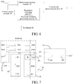
- the current source module 30 includes an internal constant current source Iref and a current mirror unit.
- the current mirror unit includes a first PMOS transistor PM1, a second PMOS transistor PM2, a third PMOS transistor PM3, a fourth PMOS transistor PM4, a fifth PMOS transistor PM5, and a sixth PMOS transistor PM6.
- Both a source and a gate of the first PMOS transistor PM1 are connected to a positive terminal of the internal constant current source Iref, and a negative terminal of the internal constant current source Iref is grounded.
- Both a source and a gate of the second PMOS transistor PM2 are connected to a drain of the first PMOS transistor PM1, and a drain of the second PMOS transistor PM2 is connected to an internal power supply POWER.
- a drain of the third PMOS transistor PM3 is connected to the detection processing module, and a gate of the third PMOS transistor PM3 is connected to the gate of the first PMOS transistor PM1.
- a drain of the fourth PMOS transistor PM4 is connected to a source of the third PMOS transistor PM3, a gate of the fourth PMOS transistor PM4 is connected to the gate of the second PMOS transistor PM2, and a source of the fourth PMOS transistor PM4 is connected to the internal power supply POWER.
- a drain of the fifth PMOS transistor PM5 is connected to the detection similarity processing module 20, and a gate of the fifth PMOS transistor PM5 is connected to the gate of the first PMOS transistor PM1.
- a drain of the sixth PMOS transistor PM6 is connected to a source of the fifth PMOS transistor PM5, a gate of the sixth PMOS transistor PM6 is connected to the gate of the second PMOS transistor PM2, and a source of the sixth PMOS transistor PM6 is connected to the internal power supply POWER.
- the detection processing module 10 includes a first resistor R1, a seventh PMOS transistor PM7, and a second resistor R2.
- One end of the first resistor R1 is connected to the current source module 30 and the comparison processing module 40.
- a source of the seventh PMOS transistor PM7 is connected to the other end of the first resistor R1, and a gate of the seventh PMOS transistor PM7 is connected to the voltage sampling end VIN.
- One end of the second resistor R2 is connected to a drain of the seventh PMOS transistor PM7, and the other end of the second resistor R2 is grounded.
- the detection similarity processing module 20 includes an eighth PMOS transistor PM8 and a third resistor R3.
- a source of the eighth PMOS transistor PM8 is connected to the resistance trimming unit 201, and a gate of the eighth PMOS transistor PM8 is grounded.
- One end of the third resistor R3 is connected to a drain of the eighth PMOS transistor PM8, and the other end of the third resistor R3 is grounded.
- the resistance trimming unit 201 includes a trimming resistor R X and a fuse fuse.
- One end of the trimming resistor R X is connected to the current source module 30 and the comparison processing module 40, and the other end of the trimming resistor R X is connected to the source of the eighth PMOS transistor PM8.
- the fuse fuse and the trimming resistor R X are connected in parallel.
- the comparison processing module 40 includes a comparator 401 and a phase inverter 402.
- a positive input terminal of the comparator 401 is connected to the detection similarity processing module 20, and a negative input terminal of the comparator 401 is connected to the detection processing module 10.
- An input terminal of the phase inverter 402 is connected to an output terminal of the comparator 401, and an output terminal of the phase inverter 401 is configured to output the voltage detection signal.
- branch currents of the detection processing module 10 and the detection similarity processing module 20 are theoretically equivalent, and are both equivalent to a current of the internal constant current source Iref.
- the branch current of the detection processing module 10 is I VIN
- a total resistance of the first resistor R1 and the second resistor R2 is R VIN
- a threshold VTH7 for turning on the seventh PMOS transistor PM7 is a fixed attribute parameter value
- a threshold VTH8 for turning on the eighth PMOS transistor PM8 is assumed to be a fixed attribute parameter value.
- a target voltage of the voltage sampling end VIN is V VIN0
- an actual resistance needing to be trimmed by the trimming resistor R X is R X0
- VN V VIN0 + I VIN ⁇ R VIN + VTH7
- VP VTH8 + I T ⁇ R30 + I T ⁇ R X0 .
- the actual value R X0 needing the trimming resistor is (V VIN0 - V VIN1 ) / I T .
- the trimming resistor R X and the third resistor R3 are placed in a same region, and it may be approximately considered that deviation ratios of the two resistors are consistent.
- the actual value of the third resistor R3 is R30, and a theoretical value is R31;
- the sampling voltage V VIN1 of the voltage sampling end VIN is basically equivalent to the target voltage V VIN0 .
- the phase inverter 402 outputs a determination result from the OUT port.
- the sampling voltage V VIN1 of the voltage sampling end VIN is related with only the actual value of R3 and a value of I T . Even though the sampling voltage is very small, the sampling voltage may also be precisely detected and determined. If the foregoing circuit is applied to a battery pack, charging and discharging states of the battery pack may be correctly identified.
- the detection processing module outputs the first detection voltage after performing level shift processing on the voltage sampled by the voltage sampling end, the detection similarity processing module imitates the detection processing module, to generate the reference voltage, then the current source module provides the bias current to the detection processing module and the detection similarity processing module, and finally the comparison processing module performs comparison processing on the first detection voltage and the reference voltage, to detect and determine the voltage sampled by the voltage sampling end.
- the circuit does not need a reference voltage, and has a simple circuit structure. Moreover, there is no need to consider an influence caused by an offset voltage of a comparator. A voltage sampled by a sampling end may be accurately detected and determined, so that charging and discharging states of a battery pack may be correctly identified.
- an embodiment of the present invention further provides a power battery system, including the foregoing voltage detection and determination circuit.
- the detection similarity processing module is used to imitate the detection processing module, to generate a reference voltage.
- a reference voltage is not needed, and a circuit structure is simple. Moreover, there is no need to consider an influence caused by an offset voltage of a comparator. A voltage sampled by a sampling end may be accurately detected and determined, so that charging and discharging states of a battery pack may be correctly identified.
- an orientation or position relationship indicated by the term such as "central”, “longitudinal”, “transverse”, “length”, “width”, “thickness”, “above”, “below”, “front”, “rear”, “left”, “right”, “vertical”, “horizontal”, “top”, “bottom”, “internal”, “external”, “clockwise”, “anticlockwise”, “axial”, “radial”, or “circumferential”, is an orientation or position relationship shown based on the accompanying drawings.
- the term is used only for ease of description of the present invention and simplification of description, rather than indicating or implying that an indicated apparatus or element needs to have a particular orientation and to be constructed and operated at the particular orientation. Therefore, the terms cannot be constructed as limitation to the present invention.
- first and second are only used for the purpose of description, but cannot be constructed as indication or implication of relative importance or implied indication of quantities of indicated technical features. Therefore, features limited by the “first” and the “second” may expressly or impliedly indicate that at least one of the features is included.
- the meaning of “multiple” means at least two, for example, two or three, unless it is expressly and specifically defined.
- connection may be fixed connection, may be removable connection, or may be integrated into one; may be mechanical connection, or may be electric connection; or may be direct connection, may be indirect connection by using an intermediate medium, may be communication inside two elements, or may be a relationship of interaction between two elements, unless otherwise clearly limited.
- connection may be fixed connection, may be removable connection, or may be integrated into one; may be mechanical connection, or may be electric connection; or may be direct connection, may be indirect connection by using an intermediate medium, may be communication inside two elements, or may be a relationship of interaction between two elements, unless otherwise clearly limited.
- a first feature “above” or “below” a second feature may be that the first feature is in direct contact with the second feature, or the first feature is in indirect contact with the second feature by using an intermediate medium.
- the first feature “above”, “over” or “on” the second feature may be that the first feature may be above the second feature, or merely indicates that a level of the first feature is higher than that of the second feature.
- the first feature “below”, “beneath” or “under” the second feature may be that the first feature may be below the second feature, or merely indicates that a level of the first feature is less than that of the second feature.
- description of the reference term such as "an embodiment”, “some embodiments”, “an example”, “a specific example”, or “some examples” means that a specific feature, a structure, a material or a characteristic that is described with reference to the embodiment or example is included in at least one embodiment or example of the present invention.
- schematic description of the foregoing terms is unnecessarily for a same embodiment or example.
- the described specific feature, structure, material or characteristic may be combined in any proper manner in any one or multiple embodiments or examples.
- a person skilled in the art may integrate and combine different embodiments or examples described in this specification or features thereof as long as no conflict occurs.
Landscapes
- Physics & Mathematics (AREA)
- General Physics & Mathematics (AREA)
- Engineering & Computer Science (AREA)
- Power Engineering (AREA)
- Secondary Cells (AREA)
- Measurement Of Current Or Voltage (AREA)
Applications Claiming Priority (2)
| Application Number | Priority Date | Filing Date | Title |
|---|---|---|---|
| CN201610402877.2A CN107478992B (zh) | 2016-06-08 | 2016-06-08 | 电压检测与判断电路和具有其的动力电池系统 |
| PCT/CN2017/086005 WO2017211193A1 (fr) | 2016-06-08 | 2017-05-25 | Circuit de détection et de détermination de tension, et système de batterie d'alimentation le comprenant |
Publications (2)
| Publication Number | Publication Date |
|---|---|
| EP3470860A1 true EP3470860A1 (fr) | 2019-04-17 |
| EP3470860A4 EP3470860A4 (fr) | 2019-07-10 |
Family
ID=60577572
Family Applications (1)
| Application Number | Title | Priority Date | Filing Date |
|---|---|---|---|
| EP17809632.7A Withdrawn EP3470860A4 (fr) | 2016-06-08 | 2017-05-25 | Circuit de détection et de détermination de tension, et système de batterie d'alimentation le comprenant |
Country Status (4)
| Country | Link |
|---|---|
| US (1) | US20190257860A1 (fr) |
| EP (1) | EP3470860A4 (fr) |
| CN (1) | CN107478992B (fr) |
| WO (1) | WO2017211193A1 (fr) |
Families Citing this family (7)
| Publication number | Priority date | Publication date | Assignee | Title |
|---|---|---|---|---|
| CN109239582B (zh) * | 2018-10-19 | 2023-12-15 | 上海芯哲微电子科技股份有限公司 | 一种充电管理集成电路的测试装置 |
| CN111596247B (zh) * | 2020-01-13 | 2023-04-11 | 国网天津市电力公司 | 一种电压检测电路及方法 |
| CN111562806B (zh) * | 2020-05-18 | 2024-06-04 | 拓尔微电子股份有限公司 | Cmos工艺上实现低温度系数电压及电流的参考源电路 |
| CN112285473A (zh) * | 2020-10-30 | 2021-01-29 | 尹永云 | 一种电动自行车电池过放电检测装置 |
| US11323111B1 (en) * | 2021-01-04 | 2022-05-03 | Realtek Semiconductor Corp. | High-frequency signal detector and method thereof |
| CN115912560B (zh) * | 2022-12-02 | 2025-04-04 | 深圳达人高科电子有限公司 | 锂电池低压差限流电路及对应的锂电池充电保护系统 |
| CN118465604B (zh) * | 2024-05-06 | 2025-01-21 | 上海川土微电子有限公司 | 一种负电源开路检测电路和驱动芯片 |
Family Cites Families (20)
| Publication number | Priority date | Publication date | Assignee | Title |
|---|---|---|---|---|
| FR2412850A1 (fr) * | 1977-04-26 | 1979-07-20 | Suwa Seikosha Kk | Circuit integre a semi-conducteurs |
| JPS61140880A (ja) * | 1984-12-13 | 1986-06-27 | Toshiba Corp | 電池電圧検出回路 |
| JP3451954B2 (ja) * | 1998-08-26 | 2003-09-29 | 日産自動車株式会社 | 電圧比較回路 |
| JP2002372554A (ja) * | 2001-06-13 | 2002-12-26 | Ricoh Co Ltd | 電圧検出回路 |
| US7171327B2 (en) * | 2004-03-24 | 2007-01-30 | Infineon Technologies Ag | Temperature sensor scheme |
| JP2006112906A (ja) * | 2004-10-14 | 2006-04-27 | Sanyo Electric Co Ltd | 電圧検出回路 |
| KR100778287B1 (ko) * | 2005-02-04 | 2007-11-22 | (주)퓨얼셀 파워 | 전지 전압 감시 장치 및 이를 이용하는 전지 |
| CN101140302A (zh) * | 2006-09-07 | 2008-03-12 | 普立尔科技股份有限公司 | 电池电压准位的侦测装置以及侦测方法 |
| CN101144836A (zh) * | 2006-09-11 | 2008-03-19 | 精拓科技股份有限公司 | 电压检测电路及其方法 |
| CN101281216B (zh) * | 2008-05-28 | 2011-10-12 | 北京中星微电子有限公司 | 一种采用扫描模式的电压检测电路 |
| US8633743B2 (en) * | 2009-10-15 | 2014-01-21 | Silicon Laboratories Norway As | Low power brown out detector |
| CN102136827B (zh) * | 2011-05-10 | 2013-11-06 | 覃超 | 可补偿输入失调电压的差分放大器及补偿方法 |
| JP5754343B2 (ja) * | 2011-10-25 | 2015-07-29 | ミツミ電機株式会社 | 低電圧検出回路 |
| US9362874B2 (en) * | 2013-07-10 | 2016-06-07 | Fairchild Semiconductor Corporation | Differential measurements with a large common mode input voltage |
| US9329208B2 (en) * | 2013-08-28 | 2016-05-03 | Freescale Semiconductor, Inc. | Negative voltage measurement |
| CN104467800B (zh) * | 2013-09-16 | 2018-02-09 | 比亚迪股份有限公司 | 电平移位电路 |
| CN105093048B (zh) * | 2014-04-30 | 2018-03-13 | 比亚迪股份有限公司 | 端口检测系统及具有其的车辆 |
| US9353017B2 (en) * | 2014-06-17 | 2016-05-31 | Freescale Semiconductor, Inc. | Method of trimming current source using on-chip ADC |
| CN104897949B (zh) * | 2015-05-25 | 2017-10-24 | 上海华虹宏力半导体制造有限公司 | 电压检测电路 |
| CN105467193B (zh) * | 2015-12-25 | 2018-02-27 | 无锡中感微电子股份有限公司 | 电压检测电路 |
-
2016
- 2016-06-08 CN CN201610402877.2A patent/CN107478992B/zh active Active
-
2017
- 2017-05-25 US US16/307,653 patent/US20190257860A1/en not_active Abandoned
- 2017-05-25 WO PCT/CN2017/086005 patent/WO2017211193A1/fr not_active Ceased
- 2017-05-25 EP EP17809632.7A patent/EP3470860A4/fr not_active Withdrawn
Also Published As
| Publication number | Publication date |
|---|---|
| EP3470860A4 (fr) | 2019-07-10 |
| US20190257860A1 (en) | 2019-08-22 |
| CN107478992A (zh) | 2017-12-15 |
| WO2017211193A1 (fr) | 2017-12-14 |
| CN107478992B (zh) | 2020-04-24 |
Similar Documents
| Publication | Publication Date | Title |
|---|---|---|
| EP3470860A1 (fr) | Circuit de détection et de détermination de tension, et système de batterie d'alimentation le comprenant | |
| US20040239333A1 (en) | Apparatus for judging state of assembled battery | |
| US20110115427A1 (en) | Energy storage device | |
| TWI570388B (zh) | Sensing device | |
| JP6499075B2 (ja) | 二次電池状態検出装置および二次電池状態検出方法 | |
| JP5848415B2 (ja) | 負温度係数サーミスタを利用した温度測定装置 | |
| US20170365991A1 (en) | Electrical junction box | |
| CN111044768B (zh) | 用于运行电流传感器的方法和电流传感器 | |
| CN107024294B (zh) | 一种多通道芯片温度测量电路及方法 | |
| KR20190093409A (ko) | 배터리를 위한 등가 회로 모델의 파라미터 추정 방법 및 배터리 관리 시스템 | |
| TW201303544A (zh) | 電壓調節器 | |
| JP2017049229A (ja) | バッテリ状態検知装置及びコンピュータプログラム | |
| US9812743B2 (en) | Battery state monitoring circuit and battery device | |
| US7317316B2 (en) | Apparatus and method for measuring the insulation resistance of a fuel cell system | |
| KR20150048059A (ko) | 자기 센서 회로 | |
| CN105467193A (zh) | 电压检测电路 | |
| EP3301437A1 (fr) | Circuiterie de mesure destinée à évaluer une résistance d'un détecteur résistif de gaz | |
| JP6250418B2 (ja) | ボルテージレギュレータ | |
| US7434985B2 (en) | Calibrated built-in temperature sensor and calibration method thereof | |
| US11454554B2 (en) | Temperature detection device and method using sets of DC voltages | |
| US20050038625A1 (en) | Temperature detection cell, and method to determine the detection threshold of such a cell | |
| JP3273871B2 (ja) | 電圧検出装置 | |
| US11656284B2 (en) | Method for operating a battery sensor, and battery sensor | |
| JP2007085843A (ja) | 電流センサの故障検知装置および方法 | |
| JP4456402B2 (ja) | 直流回路の地絡監視装置 |
Legal Events
| Date | Code | Title | Description |
|---|---|---|---|
| STAA | Information on the status of an ep patent application or granted ep patent |
Free format text: STATUS: THE INTERNATIONAL PUBLICATION HAS BEEN MADE |
|
| PUAI | Public reference made under article 153(3) epc to a published international application that has entered the european phase |
Free format text: ORIGINAL CODE: 0009012 |
|
| STAA | Information on the status of an ep patent application or granted ep patent |
Free format text: STATUS: REQUEST FOR EXAMINATION WAS MADE |
|
| 17P | Request for examination filed |
Effective date: 20181218 |
|
| AK | Designated contracting states |
Kind code of ref document: A1 Designated state(s): AL AT BE BG CH CY CZ DE DK EE ES FI FR GB GR HR HU IE IS IT LI LT LU LV MC MK MT NL NO PL PT RO RS SE SI SK SM TR |
|
| AX | Request for extension of the european patent |
Extension state: BA ME |
|
| A4 | Supplementary search report drawn up and despatched |
Effective date: 20190607 |
|
| RIC1 | Information provided on ipc code assigned before grant |
Ipc: G01R 31/36 20190101AFI20190603BHEP Ipc: G01R 19/165 20060101ALI20190603BHEP |
|
| DAV | Request for validation of the european patent (deleted) | ||
| DAX | Request for extension of the european patent (deleted) | ||
| STAA | Information on the status of an ep patent application or granted ep patent |
Free format text: STATUS: THE APPLICATION HAS BEEN WITHDRAWN |
|
| 18W | Application withdrawn |
Effective date: 20191211 |