EP3474355B1 - Matériau actif d'électrode négative pour dispositif électrique, et dispositif électrique dans lequel ledit matériau est utilisé - Google Patents
Matériau actif d'électrode négative pour dispositif électrique, et dispositif électrique dans lequel ledit matériau est utilisé Download PDFInfo
- Publication number
- EP3474355B1 EP3474355B1 EP16905495.4A EP16905495A EP3474355B1 EP 3474355 B1 EP3474355 B1 EP 3474355B1 EP 16905495 A EP16905495 A EP 16905495A EP 3474355 B1 EP3474355 B1 EP 3474355B1
- Authority
- EP
- European Patent Office
- Prior art keywords
- phase
- phases
- alloy
- negative electrode
- active material
- Prior art date
- Legal status (The legal status is an assumption and is not a legal conclusion. Google has not performed a legal analysis and makes no representation as to the accuracy of the status listed.)
- Active
Links
Images







Classifications
-
- H—ELECTRICITY
- H01—ELECTRIC ELEMENTS
- H01M—PROCESSES OR MEANS, e.g. BATTERIES, FOR THE DIRECT CONVERSION OF CHEMICAL ENERGY INTO ELECTRICAL ENERGY
- H01M4/00—Electrodes
- H01M4/02—Electrodes composed of, or comprising, active material
- H01M4/36—Selection of substances as active materials, active masses, active liquids
- H01M4/38—Selection of substances as active materials, active masses, active liquids of elements or alloys
- H01M4/386—Silicon or alloys based on silicon
-
- C—CHEMISTRY; METALLURGY
- C22—METALLURGY; FERROUS OR NON-FERROUS ALLOYS; TREATMENT OF ALLOYS OR NON-FERROUS METALS
- C22C—ALLOYS
- C22C28/00—Alloys based on a metal not provided for in groups C22C5/00 - C22C27/00
-
- H—ELECTRICITY
- H01—ELECTRIC ELEMENTS
- H01M—PROCESSES OR MEANS, e.g. BATTERIES, FOR THE DIRECT CONVERSION OF CHEMICAL ENERGY INTO ELECTRICAL ENERGY
- H01M4/00—Electrodes
- H01M4/02—Electrodes composed of, or comprising, active material
- H01M4/13—Electrodes for accumulators with non-aqueous electrolyte, e.g. for lithium-accumulators; Processes of manufacture thereof
- H01M4/134—Electrodes based on metals, Si or alloys
-
- H—ELECTRICITY
- H01—ELECTRIC ELEMENTS
- H01M—PROCESSES OR MEANS, e.g. BATTERIES, FOR THE DIRECT CONVERSION OF CHEMICAL ENERGY INTO ELECTRICAL ENERGY
- H01M4/00—Electrodes
- H01M4/02—Electrodes composed of, or comprising, active material
- H01M4/36—Selection of substances as active materials, active masses, active liquids
- H01M4/38—Selection of substances as active materials, active masses, active liquids of elements or alloys
-
- C—CHEMISTRY; METALLURGY
- C01—INORGANIC CHEMISTRY
- C01P—INDEXING SCHEME RELATING TO STRUCTURAL AND PHYSICAL ASPECTS OF SOLID INORGANIC COMPOUNDS
- C01P2002/00—Crystal-structural characteristics
- C01P2002/80—Crystal-structural characteristics defined by measured data other than those specified in group C01P2002/70
- C01P2002/85—Crystal-structural characteristics defined by measured data other than those specified in group C01P2002/70 by XPS, EDX or EDAX data
-
- C—CHEMISTRY; METALLURGY
- C01—INORGANIC CHEMISTRY
- C01P—INDEXING SCHEME RELATING TO STRUCTURAL AND PHYSICAL ASPECTS OF SOLID INORGANIC COMPOUNDS
- C01P2004/00—Particle morphology
- C01P2004/01—Particle morphology depicted by an image
- C01P2004/03—Particle morphology depicted by an image obtained by SEM
-
- C—CHEMISTRY; METALLURGY
- C01—INORGANIC CHEMISTRY
- C01P—INDEXING SCHEME RELATING TO STRUCTURAL AND PHYSICAL ASPECTS OF SOLID INORGANIC COMPOUNDS
- C01P2004/00—Particle morphology
- C01P2004/01—Particle morphology depicted by an image
- C01P2004/04—Particle morphology depicted by an image obtained by TEM, STEM, STM or AFM
-
- H—ELECTRICITY
- H01—ELECTRIC ELEMENTS
- H01M—PROCESSES OR MEANS, e.g. BATTERIES, FOR THE DIRECT CONVERSION OF CHEMICAL ENERGY INTO ELECTRICAL ENERGY
- H01M10/00—Secondary cells; Manufacture thereof
- H01M10/05—Accumulators with non-aqueous electrolyte
- H01M10/052—Li-accumulators
- H01M10/0525—Rocking-chair batteries, i.e. batteries with lithium insertion or intercalation in both electrodes; Lithium-ion batteries
-
- H—ELECTRICITY
- H01—ELECTRIC ELEMENTS
- H01M—PROCESSES OR MEANS, e.g. BATTERIES, FOR THE DIRECT CONVERSION OF CHEMICAL ENERGY INTO ELECTRICAL ENERGY
- H01M4/00—Electrodes
- H01M4/02—Electrodes composed of, or comprising, active material
- H01M2004/026—Electrodes composed of, or comprising, active material characterised by the polarity
- H01M2004/027—Negative electrodes
-
- Y—GENERAL TAGGING OF NEW TECHNOLOGICAL DEVELOPMENTS; GENERAL TAGGING OF CROSS-SECTIONAL TECHNOLOGIES SPANNING OVER SEVERAL SECTIONS OF THE IPC; TECHNICAL SUBJECTS COVERED BY FORMER USPC CROSS-REFERENCE ART COLLECTIONS [XRACs] AND DIGESTS
- Y02—TECHNOLOGIES OR APPLICATIONS FOR MITIGATION OR ADAPTATION AGAINST CLIMATE CHANGE
- Y02E—REDUCTION OF GREENHOUSE GAS [GHG] EMISSIONS, RELATED TO ENERGY GENERATION, TRANSMISSION OR DISTRIBUTION
- Y02E60/00—Enabling technologies; Technologies with a potential or indirect contribution to GHG emissions mitigation
- Y02E60/10—Energy storage using batteries
Definitions
- Secondary batteries for driving a motor are required to have extremely high output characteristics and high energy as compared with consumer lithium ion secondary batteries to be used in mobile phones, notebook computers, and the like. Hence, lithium ion secondary batteries having the highest theoretical energy among all batteries are attracting attention, and the development thereof is being rapidly conducted at present.
- carbon and graphite-based materials which are advantageous from the viewpoint of the life of charge and discharge cycles and cost, have been used in the negative electrode of a lithium ion secondary battery.
- charge and discharge are performed by occlusion of lithium ions into and release of the lithium ions from the graphite crystals and there is thus a disadvantage that it is impossible to obtain a charge and discharge capacity of 372 mAh/g or more of a theoretical capacity to be obtained from LiC 6 which is a compound containing lithium in the largest amount. For this reason, it is difficult to obtain a capacity and an energy density which satisfy the practical level for a vehicle application from carbon and graphite-based negative electrode materials.
- a silicide of a transition metal M particularly that of Ti (TiSi 2 ) can be refined (the modal radius of the independent first phases can be decreased), 2. the proportion of Si in the eutectic can be increased, and 3. forming ability of the amorphous (amorphous or low crystalline Si) phase can be enhanced. For these reasons, it is possible to suppress the expansion of Si during charge and discharge and to improve the cycle durability by refinement and amorphization.
- the microstructure of the alloy has a configuration in which the second phase (Si phase) is eutecticized with the first phase (TiSi 2 phase) and the eutectic further enters the gaps between a plurality of independent first phases (TiSi 2 phases).
- the first phase (TiSi 2 phase) is superior to the second phase (a-Si phase) in the hardness and electron conductivity.
- the second phase (a-Si phase) can be uniformly reacted as the second phase is eutecticized with the first phase (silicide phase) to be composed of a silicide exhibiting electrical conductivity.
- the cycle durability of the electrical device in which the negative electrode active material is used can be improved while the electrical device has a high capacity.
- a negative electrode for a lithium ion secondary battery which is a representative embodiment of a negative electrode containing the negative electrode active material for an electrical device according to the present invention, and a lithium ion secondary battery using the same
- the voltage of the cell is large and a high energy density and a high output density can be attained.
- a lithium ion secondary battery fabricated using the negative electrode active material for a lithium ion secondary battery of the present embodiment is excellent as a driving power source of vehicles and an auxiliary power source.
- it can be suitably utilized as a lithium ion secondary battery for a driving power source of vehicles and the like.
- it can be sufficiently applied to lithium ion secondary batteries for mobile devices such as mobile phones.
- the lithium ion secondary battery to be the target of the present embodiment may be any one as long as it is fabricated using the negative electrode active material for a lithium ion secondary battery of the present embodiment to be described below, and other constituent requirements thereof are not particularly limited.
- the lithium ion secondary battery in a case in which the lithium ion secondary battery is distinguished by the form and structure, the lithium ion secondary battery can be applied to any conventionally known form and structure such as a stacked type (flat type) battery and a wound type (cylindrical type) battery. It is advantageous from the viewpoint of cost and workability to adopt a stacked type (flat type) battery structure since long-term reliability can be secured by a simple sealing technique such as thermocompression bonding.
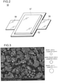
- the outermost layer negative electrode current collector may be positioned on both outermost layers of the power generating element 21 by reversing the disposition of the positive electrode and the negative electrode from that in Fig. 1 , and thus the negative electrode active material layer may be disposed on one side or both sides of the outermost layer negative electrode current collector.
- the NMC complex oxide also includes a complex oxide in which a part of transition metal elements is substituted with other metal elements.
- other elements in that case may include Ti, Zr, Nb, W, P, Al, Mg, V, Ca, Sr, Cr, Fe, B, Ga, In, Si, Mo, Y, Sn, V, Cu, Ag, and Zn, Ti, Zr, Nb, W, P, Al, Mg, V, Ca, Sr, and Cr are preferable, Ti, Zr, P, Al, Mg, V, Ca, Sr, and Cr are more preferable, and Ti, Zr, Al, Mg, and Cr are still more preferable from the viewpoint of improving the cycle characteristics.
- M is at least one kind of element selected from Ti, Zr, Nb, W, P, Al, Mg, V, Ca, Sr, or Cr) since the theoretical discharge capacity is high.
- the crystal structure is stabilized as at least one kind selected from the group consisting of Ti, Zr, Nb, W, P, Al, Mg, V, Ca, Sr, and Cr forms a solid solution and, as a result, a decrease in the capacity of the battery can be prevented even when charge and discharge are repeatedly performed and excellent cycle characteristics can be realized.
- b, c, and d satisfy 0.44 ⁇ b ⁇ 0.51, 0.27 ⁇ c ⁇ 0.31, and 0.19 ⁇ d ⁇ 0.26 in General Formula (1) from the viewpoint of improving the balance between capacity and life span characteristics.
- two or more kinds of positive electrode active materials may be used concurrently.
- a lithium-transition metal complex oxide is used as a positive electrode active material from the viewpoint of capacity and output characteristics.
- positive electrode active materials other than those described above may be used.
- a value to be calculated as an average value of particle diameters of particles to be observed in from several to several tens of visual fields by using observation means such as a scanning electron microscope (SEM) and a transmission electron microscope (TEM) is adopted as the value of "average particle diameter”.
- SEM scanning electron microscope
- TEM transmission electron microscope
- the particle diameter and average particle diameter of other constituents can be defined in the same manner.
- the positive electrode active material layer 15 may contain a binder.
- a binder is added for the purpose of maintaining the electrode structure by binding the active materials to each other or the active material with the current collector.
- the binder to be used in the positive electrode active material layer is not particularly limited, but examples thereof may include the following materials.
- Thermoplastic polymers such as polyethylene, polypropylene, polyethylene terephthalate (PET), polyether nitrile (PEN), polyacrylonitrile, polyimide, polyamide, polyamideimide, cellulose, carboxymethyl cellulose (CMC), an ethylene-vinyl acetate copolymer, polyvinyl chloride, styrene-butadiene rubber (SBR), isoprene rubber, butadiene rubber, ethylene-propylene rubber, an ethylene-propylene-diene copolymer, a styrene-butadiene-styrene block copolymer and any hydrogenated product thereof, and a styrene-isoprene-styrene
- polyvinylidene fluoride, polyimide, styrene-butadiene rubber, carboxymethyl cellulose, polypropylene, polytetrafluoroethylene, polyacrylonitrile, polyamide and polyamideimide are more preferable.
- These suitable binders exhibit excellent heat resistance, further have an extremely wide potential window, are stable to both the positive electrode potential and the negative electrode potential, and can be used in the active material layers.
- One kind of these binders may be used singly or two kinds thereof may be used concurrently.
- the negative electrode active material layer 13 contains a negative electrode active material.
- the silicon-containing alloy constituting the negative electrode active material in the aspect (first aspect) focused on the alloy composition of the silicon-containing alloy has a composition to be represented by the following Chemical Formula (1) .
- the negative electrode active material has the the microstructure described above (second aspect) as well, the phase transformation between the amorphous phase and the crystalline phase of the Si phase at the time of charge is suppressed, thus the collapse of the particles themselves can be suppressed, the function (high capacity) as an active material is maintained, and the cycle life can be improved.
- the silicon-containing alloy constituting the negative electrode active material of the present embodiment has the alloy fine structure described above (second aspect) as it has the alloy composition described above (first aspect). Moreover, the silicon-containing alloy has an action due to the microstructure, and as a result, it can exhibit an effect that the expansion of Si at the time of charge and discharge can be suppressed and cycle durability can be improved.
- the microstructure thereof has a configuration in which the second phase (Si phase) is eutecticized with the first phase (TiSi 2 phase) and the eutectic further enters the gaps between a plurality of independent first phases (TiSi 2 phases).
- the first phase (TiSi 2 phase) is superior to the second phase (a-Si phase) in the hardness and electron conductivity.
- the expansion of the second phase (a-Si phase) in the eutectic structure in the charge and discharge process can be suppressed by so-called two step repression that the expansion is repressed by the eutecticized first phase (TiSi 2 phase) and further by a plurality of independent first phases (TiSi 2 phases) .
- the second phase (a-Si phase) can be uniformly reacted as the second phase is eutecticized with the first phase (silicide phase) to be composed of a silicide exhibiting electrical conductivity.
- the cycle durability of the electrical device in which the negative electrode active material is used can be improved while the electrical device has a high capacity.
- proeutectic TiSi 2 can be refined, and independent proeutectic TiSi 2 phases are finely dispersed in the structure, thus the expansion and shrinkage of Si associated with charge and discharge can be effectively suppressed, and the durability can be improved.
- the expansion of Si can be effectively repressed even if the ratio of the modal radius between eutectic TiSi 2 and eutectic Si is set to 1 or less, that is, the eutectic TiSi 2 is set to be relatively small with respect to the Si phase.
- Si and Al are attracted to each other in the liquid phase but repel each other in the solid phase as described above, thus the stability of the Si-containing alloy in the liquid state is relatively high when Al is added to the Si-Sn-Ti alloy, and this makes it possible to enhance forming ability of the amorphous phase of the Si-containing alloy and to increase the degree of amorphousness. For this reason, the chemical structure of the a-Si phase (second phase) is hardly changed even at the time of intercalation and deintercalation of Li associated with charge and discharge, and it is possible to exhibit still higher durability.
- the silicon-containing alloy (having a composition of Si x Sn y M z Al w A a ) has a composition in which a small amount of Al is added to a ternary alloy of Si, Sn and M (transition metal selected from the group consisting of Ti, Zr, Ni, Cu, Mo, Nb, Sc, Co, Cr and Fe) (quaternary alloy composition) . It is possible to realize high cycle durability by having such a composition.
- y composition ratio of Sn: % by mass
- y is preferably 10 or less, more preferably 9 or less, and still more preferably 8.5 or less. Further, y is preferably 2 or more and still more preferably 3 or more. It is excellent that y is in such a range from the viewpoint of being able to reversibly intercalate and deintercalate Li ions at the time of charge and discharge since Sn forms a solid solution in the second phase (Si phase) and increases the distance between the Si tetrahedrons in the Si phase, and it is possible to sufficiently improve the durability and to more efficiently exert the effect of the present invention.
- z composition ratio of the transition metal element M: % by mass
- z is preferably 35 or less, more preferably 34 or less, still more preferably 33 or less, yet more preferably 32 or less, and particularly preferably 31 or less.
- z is preferably 25 or more, more preferably 28 or more, and still more preferably 29 or more. It is excellent that z is in such a range from the viewpoint of the balance between the maintenance of durability against charge and discharge (intercalation and deintercalation of Li ions) and the initial capacity, and it is possible to sufficiently improve the durability, to obtain a high capacity, and to more efficiently exert the effect of the present invention.
- w composition ratio of Al: % by mass
- w is preferably 3 or less, more preferably 2.5 or less, and still more preferably 2.0 or less.
- w is preferably 0.3 or more, more preferably 0.35 or more, and more preferably 0.4 or more. It is excellent that w is in such a range from the viewpoint of being able to refine the proeutectic silicide precipitate, to keep the eutecticized ratio of silicide high, and to decrease the critical cooling velocity for amorphization, and it is possible to sufficiently improve the durability and to more efficiently exert the effect of the present invention.
- the range of x is not particularly limited as long as y, z, and w are in the above ranges.
- x is preferably 70 or less, more preferably 68 or less, still more preferably 67 or less, and particularly preferably 66 or less.
- x is preferably 58 or more, more preferably 58.5 or more, and still more preferably 59 or more.
- a microstructural constitution of the silicon-containing alloy according to the present embodiment can be obtained as the silicon-containing alloy contains a transition metal element M, particularly Ti, in a relatively large amount, Sn in a certain amount, and Al in a small amount while containing Si as a main component as described above.
- Sn and Al can be sufficiently dispersed and form a solid solution in part of the Si phase as a transition metal element M (preferably Ti) is selected as an element to be added to a negative electrode active material (Si-containing alloy; that is, Si as a main component), Sn is further added as a second additive element in the above range, and Al is further added as a third additive element in a small amount in the above range.
- Sn can be finely dispersed (form a solid solution) in the Si phase (see Figs. 8(b) to 8(e)).
- Al can be comparatively uniformly dispersed in the entire region of the Si phase (Al can be eutecticized with Si in part) (see Figs. 9(b) to 9(e) ).
- the chemical structure of the a-Si phase (second phase) is hardly changed even at the time of intercalation and deintercalation of Li associated with charge and discharge, and it is possible to obtain still higher durability.
- Sn and Al which are not dispersed or form a solid solution in part of the Si phase do not segregate as crystalline Sn or Al in the Si phase but crystallize at the boundary portion between the silicide phase and Si phase of the eutectic structure in the microstructure and further at the boundary portion between the independent silicide phase and the eutectic structure and the like.
- Sn functions as a Sn active material and thus sufficient cycle durability can be obtained while a high capacity is maintained.
- the suitable numerical ranges of the composition ratios of the respective constituent elements described above merely illustrate the respective preferred embodiments, and the ranges are within the technical scope of the present invention as long as they are included in the scope of claims.
- the "inevitable impurities” means those contained in the Si-containing alloy since they have been present in the raw materials or inevitably mixed in the manufacturing process. The inevitable impurities are originally unnecessary, but they are allowable impurities since they are contained in a trace amount and do not affect the characteristics of the Si alloy.
- a is preferably less than 0.5 and more preferably less than 0.1. It is possible to confirm whether or not the negative electrode active material (silicon-containing alloy) has the composition to be represented by the Chemical Formula (1) above through qualitative analysis by fluorescent X-ray analysis (XRF) and quantitative analysis by inductively coupled plasma (ICP) emission spectroscopy.
- M is a silicide forming element which is at least one kind selected from the group consisting of Ti, Zr, Ni, Cu, Mo, Nb, Sc, Co, Cr, and Fe, preferably at least one kind selected from Ti and Zr, and particularly preferably Ti.
- These elements have higher electron conductivity than silicides of other elements when forming a silicide and have a high strength.
- the negative electrode active material has a higher capacity than a conventional negative electrode active material (for example, carbon-based negative electrode active material) by this.
- M is titanium (Ti) in the composition to be represented by the Chemical Formula (1) above.
- the particle diameter of the Si-containing alloy constituting the negative electrode active material in the present embodiment is not particularly limited, but it is preferably from 0.1 to 20 ⁇ m and more preferably from 0.2 to 10 ⁇ m as an average particle diameter D50.
- the particle diameter is preferably from 5 to 30 ⁇ m and more preferably from 10 to 25 ⁇ m as an average particle diameter D90.
- the microstructure thereof has a configuration in which the second phase (Si phase) is eutecticized with the first phase (silicide phase) and the eutectic further enters the gaps between a plurality of independent first phases (silicide phases) .
- the first phase (silicide phase) for example, the TiSi 2 phase is superior to the second phase (Si phase), for example, a-Si phase in the hardness and electron conductivity.
- the first phase (silicide phase) contains a silicide (silicide) of a transition metal as a main component, and thus M is one or more kinds of transition metal elements selected from the above silicide forming elements.
- M is the silicide forming element which constitutes the first phase (silicide phase) in a case in which M is one transition metal element.
- at least one kind of M is a silicide forming element which constitutes the first phase (silicide phase).
- the rest of the transition metal elements may be a transition metal element to be contained in the second phase (a-Si phase) or a silicide forming element which constitutes the first phase (silicide phase).
- the rest of the transition metal elements may be a transition metal element which constitutes a phase (transition metal phase) formed as a transition metal crystallizes other than the first phase and the second phase (a-Si phase).
- Si-containing alloy negative electrode active material having the preferred microstructural constitution
- this silicide phase (first phase) contains a silicide (for example, TiSi 2 ) of a transition metal, and thus it exhibits excellent affinity for the a-Si phase (second phase) and can suppress cracking at the (crystal) interface particularly by the volume expansion at the time of charge.
- a silicide for example, TiSi 2
- second phase a silicide of a transition metal
- the negative electrode active material (Si-containing alloy) of the present invention has a higher capacity than a conventional negative electrode active material (for example, carbon-based negative electrode active material) by this. Consequently, it is preferable that the silicide phase (first phase) containing a silicide (silicide) of a transition metal as a main component in the microstructure is titanium silicide (TiSi 2 ).
- silicide phase to contain a silicide "as a main component" means that the silicide accounts for 50% by mass or more, preferably 80% by mass% or more, still more preferably 90% by mass or more, particularly preferably 95% by mass or more, and most preferably 98% by mass or more of the silicide phase.
- the alloy can contain inevitable impurities which have been present in the raw materials or inevitably mixed in the manufacturing process. It is thus practically difficult to obtain the first phase containing silicide at 100% by mass.
- Second phase (amorphous Si phase (a-Si phase)) containing Al in part and amorphous or low crystalline Si as main component
- a net pattern (lattice-like spot) in two-dimensional point arrangement is obtained for a single crystal phase
- a Debye-Scherrer ring (diffraction ring) is obtained for a polycrystalline phase
- a halo pattern is obtained for an amorphous phase by electron diffraction analysis.
- Sn which is dispersed and forms a solid solution inside the crystal structure of Si
- a-Si phase second phase
- carbon negative electrode material carbon negative electrode material
- proeutectic TiSi 2 can be refined, and an independent proeutectic TiSi 2 phase is finely dispersed in the structure, thus the expansion and shrinkage of Si associated with charge and discharge can be effectively suppressed, and the durability can be improved.
- the amount of TiSi 2 in the eutectic structure decreases as the amount of Al added increases since Al added remains in the liquid phase and suppresses the crystallization of TiSi 2 even when cooling further proceeds in the manufacturing process (preferably a quenching solidification method and the like), the crystallization of proeutectic TiSi 2 is completed, and a stage in which TiSi 2 is eutecticized with Si is started.
- TiSi 2 becomes relatively small with respect to Si in the eutectic structure and the Si phase and TiSi 2 phase in the eutectic structure are in the form of being adjacent to each other, thus the proportion of Si in the eutectic structure increases.
- Si and Al are attracted to each other in the liquid phase but repel each other in the solid phase, thus the stability of the Si-containing alloy in the liquid state is relatively high when Al is added to the Si-Sn-Ti alloy, and this makes it possible to enhance the amorphous phase forming ability of the Si-containing alloy and to increase the degree of amorphousness.
- the chemical structure of the a-Si phase (second phase) is hardly changed even at the time of intercalation and deintercalation of Li associated with charge and discharge, and it is possible to exhibit still higher durability (see the mechanism of action described above).
- the silicide of a transition metal of the first phase in the microstructure is titanium silicide (TiSi 2 ) and the Si phase (second phase) is Si phase containing amorphous (amorphous) Si as a main component.
- a-Si phase to contain Sn and Al and amorphous or low crystalline Si "as a main component” means that Si accounts for 50% by mass or more, preferably 80% by mass% or more, more preferably 90% by mass or more, particularly preferably 95% by mass or more, and most preferably 98% by mass or more of the Si phase.
- the alloy can contain inevitable impurities which have been present in the raw materials or inevitably mixed in the manufacturing process. It is thus practically difficult to obtain the second phase containing Si at 100% by mass.
- the Si phase (second phase) "contains Sn in part" is because a portion containing Sn is observed in the Si phase although most of the Si phase is a portion which does not almost contain Al (the Si portion functions as an active material), for example, in a case in which Fig. 7(b) and Fig. 9(b) are compared with Fig. 9(e) . It can be seen that Sn is finely dispersed in the eutectic portion particularly as a small amount of Al is added (see Fig. 7(b) and Fig. 9(b) ).
- Al is dispersed in Si and forms a solid solution or dispersed in Si in the form of being incorporated therein (see the mechanism of action described above for this effect by Al).
- To contain Al "as a main component” means that Al accounts for 50% by mass or more, preferably 80% by mass% or more, more preferably 90% by mass or more, particularly preferably 95% by mass or more, and most preferably 98% by mass or more of the Al phase.
- the alloy can contain inevitable impurities which have been present in the raw materials or inevitably mixed in the manufacturing process. It is thus practically difficult to obtain an Al phase containing Al at 100% by mass.
- the upper limit of the modal radius A of a plurality of independent first phases constituting a part of the microstructure is not particularly limited, but it is, for example, 280 nm or less, preferably 260 nm or less, more preferably 252 nm or less, still more preferably 250 nm or less, and particularly preferably 235 nm or less .
- the lower limit of the modal radius A of the independent first phases in the eutectic structure is not particularly limited, but it is preferably 160 nm or more, more preferably 170 nm or more, still more preferably 180 nm or more, and particularly preferably 190 nm or more.
- a plurality of independent first phases constituting a part of the microstructure can be finely dispersed in the microstructure as the modal radius A is in such a range. Consequently, it is possible to effectively suppress the expansion and shrinkage of Si associated with charge and discharge and thus to improve the durability.
- the microstructure has a structure of which a part has a eutectic structure composed of the first phase and the second phase.
- a part of the microstructure has a eutectic structure composed of the first phase and the second phase
- the expansion of the second phase (a-Si phase) in the eutectic structure in the charge and discharge process can be suppressed through repression by the eutecticized first phase.
- the expansion of the a-Si phase can be repressed by the eutecticized first phase (TiSi 2 phase) and the part composed of a plurality of independent first phases (TiSi 2 phase), that is, expansion of the second phase can be suppressed by two step stage repression.
- the upper limit of the modal radius B of the first phase in the eutectic structure is not particularly limited, but it is preferably 70 nm or less, more preferably 67 nm or less, particularly preferably 58 nm or less, and particularly preferably 53 nm or less.
- the lower limit of the modal radius of the first phase in the eutectic structure is not particularly limited, but it is preferably 20 nm or more, more preferably 25 nm or more, still preferably 30 nm or more, and particularly preferably 35 nm or more, and among these, the lower limit is more preferably 40 nm or more. The effect described above can be more effectively exerted as the lower limit is in such a range.
- the upper limit of the modal radius C of the second phase in the eutectic structure is not particularly limited, but it is preferably 80 nm or less, more preferably 75 nm or less, and still more preferably 70 nm or less.
- the lower limit of the modal radius of the second phase in the eutectic structure is not particularly limited, but it is preferably 40 nm or more, more preferably 45 nm or more, still more preferably 50 nm or more, and particularly preferably 57 nm or more, and among these, the lower limit is more preferably 61 nm or more. The effect described above can be more effectively exerted as the lower limit is in such a range.
- the radius distribution of the second phase in the eutectic structure is preferably from 10 to 200 nm, more preferably from 20 to 150 nm, and still more preferably from 25 to 120 nm.
- the effect described above can be more effectively exerted as the radius distribution is in such a range.
- the independent first phases proeutectic TiSi 2
- Si phase the second phase of the eutectic structure which directly contributes to charge and discharge and the expansion of Si can be thus effectively repressed.
- the ratio of the modal radius B of the first phases to the modal radius C of the second phases in the eutectic structure: D3 (modal radius B of first phases of eutectic structure/modal radius C of second phases of eutectic structure) is preferably 1.00 or less, more preferably 0.95 or less, and still more preferably 0.90 or less.
- the lower limit of the ratio of the modal radius B of the first phases to the modal radius C of the second phases in the eutectic structure: D3 is not particularly limited, but it is, for example, 0.40 or more, preferably 0.50 or more, and more preferably 0.60 or more.
- D3 is set to 1 or less, that is, the modal radius B of the first phases (TiSi 2 phase) is set to be relatively small with respect to the modal radius C of the second phases (Si phase) in the eutectic structure.
- the Si-containing alloy having the structures (1) to (4) described above is obtained as predetermined raw materials of the alloy are melted and quenched and alloyed at a predetermined cooling velocity by, for example, a liquid quenching roll solidification method and thus a plurality of the independent first phases crystallize in the liquid phase as a proeutectic, and a eutectic structure composed of the first phase and the second phase crystallizes in the liquid phase in the gap of this independent first phase.
- These elements exhibit higher electron conductivity than silicides of other elements when silicides of these elements are formed and have a high strength.
- TiSi 2 that is a silicide in a case in which the transition metal element is Ti is preferable since it exhibits extremely excellent electron conductivity.
- the transition metal element M is Ti and two or more phases (for example, TiSi 2 and TiSi) having different composition ratios exist in the silicide phase
- 50% by mass or more, preferably 80% by mass or more, more preferably 90% by mass or more, particularly preferably 95% by mass or more and most preferably 100% by mass of the silicide phase is the TiSi 2 phase.
- the transition metal element M is Ti
- Si and Ti extremely strongly bond with each other from the Si-Ti binary phase diagram of Fig. 40 .
- Si and Sn repel each other from the Si-Sn binary phase diagram of Fig. 41 .
- Ti and Sn bond with each other from the Ti-Sn binary phase diagram of Fig. 42 .
- Si and Al are attracted to each other in the liquid state but repel each other in the solid phase from the Si-Al binary phase diagram of Fig. 43 .
- Ti and Al bond with each other from the Ti-Al binary phase diagram of Fig. 44 .
- Al remains in the liquid phase and is attracted to Ti and Si and can suppress the crystallization of TiSi 2 , for example, in the case of performing cooling from a liquid state such as a quenching solidification method as Al is contained in a smaller amount as compared with that of Ti.
- Sn in the liquid phase is attracted to Ti but repels Si. The crystallization of TiSi 2 can be effectively suppressed as Al enters) .
- proeutectic TiSi 2 can be refined, an independent proeutectic TiSi 2 phase is finely dispersed in the structure, thus the expansion and shrinkage of Si associated with charge and discharge can be effectively suppressed, and the durability can be improved.
- the binary phase diagram can be calculated using the integrated thermodynamic calculation system: Thermo-Calc Ver2015a developed by Thermo-Calc software AB Sweden (Japan Agency: Itochu Techno-Solutions Corporation) and solid solution general purpose database: SSOL5 (SGTE* Solution Database, ver.5.0) as a thermodynamic database. (*SGTE: Scientific Group Thermodata Europe).
- the analyzer for example, XPS (X-ray photoelectron spectroscopy), TEM-EDX (transmission electron microscope-energy dispersive X-ray spectroscopy), STEM-EDX/EELS (scanning transmission electron microscope - energy dispersive X-ray spectroscopy/electron energy loss spectroscopy), HAADF-STEM (high-angle annular dark-field scanning transmission electron microscopic imaging), and BF-STEM (bright field-scanning transmission electron microscopic imaging) can be used.
- the analyzer (analysis method) is not limited to these, and various kinds of existing observation apparatuses (apparatus conditions, measurement conditions) to be used for the microstructure of alloy may be used.
- the microstructure of the negative electrode active material having the microstructural constitution described above will be described using an example in which the Si-containing alloy (particle) fabricated in Example 1 is used as a sample (sample) .
- the microstructural constitution of the alloy (particle) can be clarified in the same manner.
- the microstructural constitution can be analyzed by the same method.
- Figs. 4 to 10 illustrate the results obtained by analyzing the portion (gray portion) of the independent first phase (TiSi 2 phase) in Fig. 3 and the structural constitution of the eutectic portion (black portion) of the first phase with the second phase.
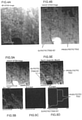
- Fig. 4(a) and Fig. 4(b) are images (low magnification) of a sample prepared from particles of a negative electrode active material (Si-containing alloy) of Example 1 by a FIB method and observed by BF-STEM (bright field-scanning transmission electron microscopic imaging) and HAADF-STEM (high-angle annular dark-field scanning transmission electron microscopic imaging).
- the object to be measured was particles of the Si-containing alloy (negative electrode active material) having an alloy composition Si 60.0 Sn 8.1 Ti 30.1 Al 1.8 (mass ratio) fabricated in Example 1.
- Fig. 5 is a diagram (low magnification) illustrating the quantitative mapping data by STEM-EDX (scanning transmission electron microscope - energy dispersive X-ray spectroscopy) .
- Fig. 5 (a) is the same HAADF-STEM image as that in Fig. 4(b) .
- Fig. 5(b) is a diagram illustrating the mapping data of Sn (on lower left) measured in the same visual field as HAADF-STEM ( Fig. 5 (a) on upper left) .
- Fig. 5 (c) is a diagram illustrating the mapping data of Si (on lower center) measured in the same visual field as HAADF-STEM ( Fig. 5(a) on upper left).
- Fig. 5 is a diagram (low magnification) illustrating the quantitative mapping data by STEM-EDX (scanning transmission electron microscope - energy dispersive X-ray spectroscopy) .
- Fig. 5 (a) is the same HAADF-STEM image as
- FIG. 5(d) is a diagram illustrating the mapping data of Ti (on lower right) measured in the same visual field as HAADF-STEM ( Fig. 5 (a) on upper left) .
- Fig. 5 (e) is a diagram (on upper right) obtained by superimposing the mapping data in Figs. 5(b) to 5(d) (Sn, Si, and Ti) measured in the same visual field as HAADF-STEM ( Fig. 5(a) on upper left) one on another.
- Fig. 6 is a diagram (low magnification) illustrating the quantitative mapping data by STEM-EDX (scanning transmission electron microscope - energy dispersive X-ray spectroscopy) .
- Fig. 6 (a) is the same HAADF-STEM image as that in Fig. 4(b) .
- Fig. 6(b) is a diagram illustrating the mapping data of Al (on lower left) measured in the same visual field as HAADF-STEM ( Fig. 6 (a) on upper left) .
- Fig. 6(c) is a diagram illustrating the mapping data of Si (on lower center) measured in the same visual field as HAADF-STEM ( Fig. 6(a) on upper left).
- Fig. 6 is a diagram (low magnification) illustrating the quantitative mapping data by STEM-EDX (scanning transmission electron microscope - energy dispersive X-ray spectroscopy) .
- Fig. 6 (a) is the same HAADF-STEM image as that
- FIG. 6(d) is a diagram illustrating the mapping data of Ti (on lower right) measured in the same visual field as HAADF-STEM ( Fig. 6 (a) on upper left) .
- Fig. 6 (e) is a diagram (on upper right) obtained by superimposing the mapping data in Figs. 6(b) to 6(d) (Al, Si, and Ti) measured in the same visual field as HAADF-STEM ( Fig. 6(a) on upper left) one on another.
- 6(b) to 6(e) can be actually colorized (colored), and thus silicide (TiSi 2 ) can be distinguished at first glance since it becomes pink in which blue of Si is mixed with red of Ti, for example, when Al is colored to green, Si to blue, and Ti to red, but it is required to submit the application drawing as a black and white image, and thus the analysis information clarified by such colorization is included in Fig. 4(b) and Figs. 6(d) and 6(e) .
- STEM-EDX scanning transmission electron microscope - energy dispersive x-ray spectroscopy
- the elastic scattering electron contrast due to the atomic number (Z) is dominant in the HAADF (high-angle annular dark-field), it is an imaging method to be also called Z-contrast imaging.
- Substances having higher atomic numbers look brighter (see Fig. 4(b), Fig. 5(a) , Fig. 6(a), Fig. 7(b) , Fig. 8(b), Fig. 9(a) , Fig. 10(a), Fig. 11(a) , and Fig. 12(a) ).
- the image is obtained by applying an electron beam thinly narrowed to the sample while scanning it and detecting the transmitted electrons scattered at a high angle among the transmitted electrons by using an annular detector.
- a heavier element is dark in the STEM image and brighter in the HAADF-STEM image since a material having a large Z 2 ⁇ is scattered at a higher angle. It is also called a Z contrast image since contrast proportional to the atomic weight (Z) is obtained.
- the composition distribution of the sample can be obtained by introducing the characteristic X-rays generated from the respective points into the EDS (energy-dispersive-spectroscopy) detector while thinly narrowing the electron beam and scanning the sample with the thinly narrowed electron beam.
- EDS energy-dispersive-spectroscopy
- the measurement can be performed at nanometer spatial resolution since there is almost no electron beam diffusion as observed in the scanning electron microscope (SEM) measurement.
- a gray portion indicating the presence of Si is confirmed at the portion corresponding to the enclosed portion on the right side of Fig. 5(e) and Fig. 6(e) in the microstructure of the sample and in the vicinity thereof.
- a gray portion indicating the presence of Sn hardly exists at the portion corresponding to the gray portion corresponding to silicide (proeutectic TiSi 2 ) at the enclosed portion on the right side of Fig. 6(e) in the microstructure of the sample and in the vicinity thereof. Rather, from the mapping data of Sn in Fig.
- the independent silicide (proeutectic TiSi 2 ) phase exists by being finely dispersed in the microstructure (for example, the enclosed portion on the right side) as can be seen from the mechanism of action described above as well.
- the microstructure of the silicon-containing alloy (particle) of the present embodiment has (1) the silicide phase (first phase) containing a silicide (silicide) of a transition metal as a main component and (3) a part of the microstructure is composed of a plurality of independent silicide phases (first phases).
- the white portion at the lower center in the drawings of Fig. 4(b) and Fig. 5(a) is ZrO 2 which was mixed at the time of pulverization of the rapidly quenched ribbon.
- the silicide phase (first phase) and the Si phase (second phase) containing Al form a eutectic structure (a structure in which the first phase and the second phase, which are (solid solution) crystals having component ratios different from each other or amorphous or low crystalline phases, are mixed together) at the enclosed portion on the left side in the microstructure of the sample and in the vicinity thereof.
- a dark gray portion (Si + Sn portion) (to be relatively small with respect to independent silicide) corresponding to the Si phase (second phase) containing Sn in part and a gray portion (to be relatively small with respect to independent silicide) corresponding to the silicide phase (first phase) are mixed together at the enclosed portion on the left side of Fig. 5 (e) and in the vicinity thereof.
- a dark gray portion (Si + Sn portion) corresponding to the Si phase (second phase) and a gray portion corresponding to the silicide phase (first phase) at the enclosed portion on the left side and in the vicinity thereof are in the form of being adjacent to each other.
- the fine Si phase and the fine silicide phase are eutecticized with each other (form a eutectic structure).
- the fact that the fine Si phase and the fine silicide phase form a eutectic structure is confirmed by the following in the case of performing colorization. That is, the (relatively small) dark gray portion (second phase) at the enclosed portion on the left side and in the vicinity thereof mainly becomes blue green in which blue of Si (containing a small amount of Sn) or blue of Si is mixed with green of Sn and the other gray portion (first phase) becomes pink in which blue of Si is mixed with red of Ti.
- this (relatively small) blue or blue-green portion corresponding to the Si phase (second phase) containing Sn and the (relatively small) pink portion corresponding to the silicide phase (first phase) form a eutectic structure from the fact that these are mixed together.
- the fine Si phase and the fine silicide phase are eutecticized with each other (form a eutectic structure).
- the fact that the fine Si phase and the fine silicide phase form a eutectic structure is confirmed by the following in the case of performing colorization.
- the (relatively small) dark gray portion (second phase) at the enclosed portion on the left side and in the vicinity thereof mainly becomes blue green in which blue of Si (containing a small amount of Al) or blue of Si is mixed with green of Al and the other gray portion (first phase) becomes pink in which blue of Si is mixed with red of Ti.
- mapping data of Ti in Fig. 5(d) when viewed in black and white images as well, from the mapping data of Ti in Fig. 5(d) , it is confirmed that a large number of (relatively small) gray portions indicating the presence of Ti exist by being dotted at the enclosed portion on the left side in the microstructure of the sample and in the vicinity thereof. Furthermore, from the mapping data of Si in Fig. 5(c) , a gray portion indicating the presence of Si is confirmed at the entire portion corresponding to the enclosed portion on the left side of Fig. 5(d) in the microstructure of the sample and in the vicinity thereof. In addition, from the comparison between the mapping data of Sn in Fig. 5(b) and the mapping data of Ti in Fig.
- the microstructure of the silicon-containing alloy (particle) of the present embodiment has (1) the silicide phase (first phase) containing a silicide (silicide) of a transition metal as a main component and (2) the second phase (Si phase, preferably amorphous Si phase (a-Si phase)) containing Sn and Al in part and amorphous or low crystalline Si (specifically, obtained as Sn and Al are dispersed in Si and form a solid solution (dispersed in a solid solution state) or Sn and Al are dispersed in Si in the form of being incorporated therein) as a main component and (4) a part of the microstructure has a eutectic structure composed of the first phase and the second phase.
- the dark gray (or black) portion is the a-Si phase (second phase) containing Sn and Al in part in the eutectic structure
- the whitish portion is the Sn phase containing Sn (crystallized because of an excess amount to be dispersed in the second phase and to form a solid solution) as a main component (or a phase containing Sn and Al; a small amount of Si and Ti may be contained; see Fig. 9 and Fig. 10 for details).
- Some of these are indicated by arrows in Fig. 7(b) so as to show which one is TiSi 2 (silicide phase), Si (a-Si phase containing Sn and Al) or Sn (Sn phase).
- the gray portion in Fig. 8(b) is the silicide (TiSi 2 ) phase (first phase) in the eutectic structure
- the dark gray (or black) portion is the a-Si phase (second phase) containing Sn and Al in the eutectic structure
- the whitish portion is the Sn phase containing Sn (crystallized because of an excess amount to be dispersed in the second phase and to form a solid solution) as a main component (or a phase containing Sn and Al; a small amount of Si and Ti may be contained; see Fig. 9 and Fig. 10 for details).
- FIG. 9(d) is a diagram illustrating the mapping data of Ti (on lower right) measured in the same visual field as HAADF-STEM ( Fig. 9 (a) on upper left) .
- Fig. 9 (e) is a diagram (on upper right) obtained by superimposing the mapping data in Figs. 9(b) to 9(d) (Sn, Si, and Ti) measured in the same visual field as HAADF-STEM ( Fig. 9(a) on upper left) one on another.
- the mapping in Figs. 9(b) is a diagram illustrating the mapping data of Ti (on lower right) measured in the same visual field as HAADF-STEM ( Fig. 9 (a) on upper left) .
- Fig. 9 (e) is a diagram (on upper right) obtained by superimposing the mapping data in Figs. 9(b) to 9(d) (Sn, Si, and Ti) measured in the same visual field as HAADF-STEM ( Fig. 9(a) on upper left
- Fig. 10 is a diagram (high magnification) illustrating the quantitative mapping data by STEM-EDX (scanning transmission electron microscope - energy dispersive X-ray spectroscopy).
- Fig. 10(a) is the same HAADF-STEM image as that in Fig. 8(b) .
- Fig. 10 (b) is a diagram illustrating the mapping data of Al (on lower left) measured in the same visual field as HAADF-STEM ( Fig. 10(a) on upper left) .
- Fig. 10(c) is a diagram illustrating the mapping data of Si (on lower center) measured in the same visual field as HAADF-STEM ( Fig. 10(a) on upper left) .
- Fig. 10 is a diagram (high magnification) illustrating the quantitative mapping data by STEM-EDX (scanning transmission electron microscope - energy dispersive X-ray spectroscopy).
- Fig. 10(a) is the same HAADF-STEM image as that in
- Figs. 9 (b) to 9(d) the portions at which Sn, Si, and Ti each do not exist are represented in black and the portions at which these elements exist are represented in gray or white. This makes it possible to confirm the presence and distribution state of Si, Sn, and Ti which are elements constituting the active material alloy Si 60.0 Sn 8.1 Ti 30.1 Al 1.8 (the negative electrode active material of Example 1) of an object to be measured.
- the portions at which Al, Si, and Ti each do not exist are represented in black and the portions at which these elements exist are represented in gray or white. This makes it possible to confirm the presence and distribution state of Si, Al, and Ti which are elements constituting the active material alloy Si 60 Sn 8.1 Ti 30.1 Al 1.8 (the negative electrode active material of Example 1) of an object to be measured.
- Fig. 9(a) on the upper left With the mapping data obtained by superimposing Sn, Si, and Ti one on another in Fig. 9(e) on the upper right, it is confirmed that the silicide phase (first phase) and the Si phase (second phase) containing Sn in part form a eutectic structure (a structure in which the first phase and the second phase, which are (solid solution) crystals having component ratios different from each other or amorphous or low crystalline phases, are mixed together).
- Fig. 10(a) on the upper left with the mapping data obtained by superimposing Al, Si, and Ti one on another in Fig.
- the dark gray portions (second phases) of the upper left, left center, lower left, upper center, lower center, upper left, and lower left portions and the like in Fig. 9(e) mainly become blue green in which blue of Si (containing a small amount of Sn) or blue of Si is mixed with green of Sn.
- the other gray portions (first phases) of the upper left, left center, upper center, center, lower center, upper right, right center, and lower right portions and the like in Fig. 9(e) become pink in which blue of Si is mixed with red of Ti.
- this blue or blue-green portion corresponding to the Si phase (second phase) containing Sn in part and the pink portion corresponding to the silicide phase (first phase) form a eutectic structure from the fact that these are mixed together.
- black in Fig. 10(a) and the dark gray portion (Si + Al Portion) in Fig. 10(e) which correspond to the Si phase (second phase) containing Al in part, and the gray portion corresponding to the silicide phase (first phase) are mixed together in Figs. 10(a) and 10(e) .
- Fig. 10(a) and the dark gray portion in Fig. 10(e) which correspond to the Si phase (second phase) containing Al in part, are dotted at the upper left, left center, lower left, upper center, lower center, upper left, and lower left portions and the like in Fig. 10(e) .
- the silicide phase (first phase) and the Si phase (second phase) containing Sn in part form a eutectic structure in the microstructures of Figs. 9(a) to 9(e) .
- the silicide phase (first phase) and the Si phase (second phase) containing Sn and Al in part form a eutectic structure in the microstructures of Figs. 10(a) to 10(e) .
- the fact that the first phase and the second phase form a eutectic structure is confirmed by the following in the case of performing colorization.
- Figs. 9(d) and 10(d) it can be seen that Ti is not present or is not almost present at the blue portions in Figs. 9(e) and 10(e) .
- the blue portions in Figs. 9(e) and 10(e) are the Si phase.
- the pink portion is a portion in which blue (the portion at which Si is present) in Figs.
- Fig. 11 and Fig. 12 are the same HAADF-STEM images as those in Fig. 8(b), Fig. 9(a) , and Fig. 10(a) and diagrams in which the regions (two places surrounded with a square frame) for observing the presence of elements in the silicide phase (first phase) and elements in the Si phase (second phase) by elemental analysis are distinguished by numerals 1 and 2 in the image.
- the silicide phase (first phase) and the Si phase (second phase) containing Sn and Al in part form a eutectic structure in the microstructure of the Si-containing alloy of Example 1.
- the microstructure of the Si-containing alloy of Example 1 has a silicide phase (first phase) containing a silicide (silicide) of a transition metal as a main component and an a-Si phase (second phase) containing Sn and Al in part and amorphous or low crystalline Si as a main component and a part of the microstructure is composed of a plurality of independent first phases and a part of the microstructure has a eutectic structure composed of the first phase and the second phase.
- Mother phase/precipitated phase liquid/TiSi 2 , Si (crystallized in liquid phase)
- the largest circle (diameter: 600 nm) and the smallest circle (diameter: 320 nm) based on the radius distribution (160 to 300 nm) of the independent first phases determined by the precipitation calculation described above are applied to some of the independent first phases and illustrated in Fig. 3 .
- these largest circle (diameter: 600 nm) and smallest circle (diameter: 320 nm) approximately coincide with the equivalent circular diameters (diameter distribution) of the large size and small size of the actual independent first phases as well.
- the intermediate circle having the modal diameter based on the modal radius of the Si phase (second phase) in the eutectic structure determined by the precipitation calculation described above and the largest circle and smallest circle based on the radius distribution can be applied to an electron micrograph such as a HAADF-STEM image and illustrated.
- the intermediate circle having the modal diameter based on the modal radius of these Si phases (second phases) in the eutectic structure and the largest circle and smallest circle based on the radius distribution approximately coincide with the equivalent circular diameter (average value and diameter distribution) of the actual Si phases (second phases) as well.
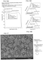
- the largest circle (diameter: 680 nm) and the smallest circle (diameter: 380 nm) based on the radius distribution (190 to 340 nm) of the independent first phases determined by the precipitation calculation described above are applied to some of the independent first phases and illustrated in Fig. 17 .
- these largest circle (diameter: 680 nm) and smallest circle (diameter: 380 nm) approximately coincide with the equivalent circular diameters (diameter distribution) of the large size and small size of the actual independent first phases as well.
- An intermediate circle (diameter: 500 nm) having the modal diameter based on the modal radius (250 nm) of the independent first phases determined by the precipitation calculation described above is applied to some of the independent first phases and illustrated in Fig. 17 .
- these intermediate circles (diameter: 500 nm) having the modal diameter approximately coincide with the equivalent circular diameter (average value) of the intermediate size of the actual independent first phases.
- the largest circle (diameter: 680 nm) and the smallest circle (diameter: 380 nm) based on the radius distribution (190 to 340 nm) of the independent first phases determined by the precipitation calculation described above are applied to some of the independent first phases and illustrated in Fig. 17 .
- these largest circle (diameter: 680 nm) and smallest circle (diameter: 380 nm) approximately coincide with the equivalent circular diameters (diameter distribution) of the large size and small size of the actual independent first phases as well.
- An intermediate circle (diameter: 500 nm) having the modal diameter based on the modal radius (250 nm) of the independent first phases determined by the precipitation calculation described above is applied to some of the independent first phases and illustrated in Fig. 20 .
- these intermediate circles (diameter: 500 nm) having the modal diameter approximately coincide with the equivalent circular diameter (average value) of the intermediate size of the actual independent first phases.
- the largest circle (diameter: 640 nm) and the smallest circle (diameter: 360 nm) based on the radius distribution (180 to 320 nm) of the independent first phases determined by the precipitation calculation described above are applied to some of the independent first phases and illustrated in Fig. 20 .
- these largest circle (diameter: 640 nm) and smallest circle (diameter: 360 nm) approximately coincide with the equivalent circular diameters (diameter distribution) of the large size and small size of the actual independent first phases as well.
- the intermediate circle having the modal diameter based on the modal radius of the Si phase (second phase) in the eutectic structure determined by the precipitation calculation described above and the largest circle and smallest circle based on the radius distribution can be applied to an electron micrograph such as a HAADF-STEM image and illustrated.
- the intermediate circle having the modal diameter based on the modal radius of these Si phases (second phases) in the eutectic structure and the largest circle and smallest circle based on the radius distribution approximately coincide with the equivalent circular diameter (average value and diameter distribution) of the actual Si phases (second phases) as well.
- the equivalent circular radius (average value) of the first phase (silicide phase) in the eutectic structure is preferably 70 nm or less, more preferably 67 nm or less, particularly preferably 58 nm or less, and particularly preferably 53 nm or less.
- the lower limit of the equivalent circular radius (average value) of the first phase (silicide phase) in the eutectic structure is not particularly limited, but it is 25 nm or more, still more preferably 30 nm or more, and particularly preferably 35 nm or more, and 40 nm or more is preferable among these. The effect described above can be more effectively exerted as the equivalent circular radius is in such a range.
- the equivalent circular radius (average value) of the second phase (Si phase) in the eutectic structure is preferably 80 nm or less, more preferably 75 nm or less, and still more preferably 70 nm or less.
- the lower limit of the equivalent circular radius (average value) of the second phase (Si phase) in the eutectic structure is not particularly limited, but it is preferably 40 nm or more, more preferably 45 nm or more, still more preferably 50 nm or more, and particularly preferably 57 nm or more, and 61 nm or more is preferable among these. The effect described above can be more effectively exerted as the equivalent circular radius is in such a range.
- the ratio of the equivalent circular radius (average value) of the independent first phase to the equivalent circular radius (average value) of the second phase of the eutectic structure in the microstructure is preferably 4.5 or less.
- the ratio is more preferably 4.3 or less, still more preferably 4.0 or less, particularly preferably 3.8 or less, and 3.6 or less is preferable among these.
- the lower limit of the ratio of the equivalent circular radius (average value) of the independent first phase to the equivalent circular radius (average value) of the second phase of the eutectic structure in the microstructure is not particularly limited, but for example, it is 2.0 or more and preferably 3.0 or more.
- the independent first phase (proeutectic TiSi 2 ) is not too large with respect to the second phase (Si phase) of the eutectic structure which directly contributes to charge and discharge as the ratio of the equivalent circular radius (average value) of the independent first phase to the equivalent circular radius (average value) of the second phase of the eutectic structure is set to 4.5 or less, and thus the expansion of Si can be effectively repressed.
- the ratio (equivalent circular radius (average value) of first phase of eutectic structure/equivalent circular radius (average value) of second phase of eutectic structure) of the equivalent circular radius (average value) of the first phase to the equivalent circular radius (average value) of the second phase in the eutectic structure is preferably 1 or less.
- the ratio is more preferably 0.95 or less and still more preferably 0.90 or less.
- the lower limit of the ratio of the equivalent circular radius (average value) of the first phase to the equivalent circular radius (average value) of the second phase in the eutectic structure is not particularly limited, but it is, for example, 0.40 or more and preferably 0.50 or more.
- the modal radii of the independent first phase and the second phase in the eutectic structure determined by the precipitation calculation described above approximately coincide with the modal radii of the actual independent first phases and the actual second phases in the eutectic structure. It has been found that the modal radii approximately coincide with the from 10 to 100, preferably from 30 to 100, and more preferably from 50 to 100 equivalent circular radii (average value) on the number basis to be measured from an electron micrograph and the like and thus the modal radius and radius distribution described above can be applied as a new index instead of these equivalent circular radii without problems.
- the method for producing the negative electrode active material for an electrical device according to the present embodiment is not particularly limited, and conventionally known knowledge can be appropriately referred to.
- the microstructure of the Si-containing alloy has a first phase and a second phase and further has a structure of which a part is composed of a plurality of independent first phases and a part has a eutectic structure composed of the first phase and the second phase.
- a method for producing a negative electrode active material composed of such a Si-containing alloy there is provided a method in which a rapidly quenched ribbon alloy is fabricated by a liquid quenching roll solidification method (also referred to simply as a "liquid quenching solidification method" in the present specification) as follows.
- a method for producing a negative electrode active material for an electrical device composed of a Si-containing alloy having a composition to be represented by the Chemical Formula (1) above which includes obtaining a negative electrode active material for an electrical device composed of the Si-containing alloy by fabricating a rapidly quenched ribbon alloy using a mother alloy having the same composition as that of the Si-containing alloy by a liquid quenching solidification method. It is possible to produce an alloy having the microstructural constitution described above by producing the negative electrode active material (Si-containing alloy) by performing the liquid quenching solidification method in this manner.
- the Si-containing alloy to be obtained it is possible to decrease the modal radius of the second phase in the eutectic structure described above, the modal radius of the independent first phase, and the like.
- a production method that can effectively contribute to the improvement in cycle durability while the Si-containing alloy active material has a high capacity.
- the Si-containing alloy (negative electrode active material) according to the present invention contains Al in a smaller amount as compared with that of Ti (transition metal element) .
- Al is attracted to Ti and Si (remains) in the liquid phase and can suppress (hinder) the crystallization of TiSi 2 .
- proeutectic TiSi 2 can be refined, and an independent (proeutectic) TiSi 2 phase (first phase) is finely dispersed in the alloy structure, and thus the expansion and shrinkage of Si associated with charge and discharge can be effectively suppressed.
- liquid quenching roll solidification method liquid quenching solidification method
- a mother alloy having the same composition as that of the desired Si-containing alloy A rapidly quenched ribbon (ribbon) alloy is fabricated by this.
- the mother alloy high purity raw materials (ingots, wires, plates, and the like of simple substances) for each of silicon (Si), tin (Sn), aluminum (Al), and transition metal (for example, titanium (Ti)) are prepared. Subsequently, a mother alloy in the form of an ingot or the like is fabricated by a known method such as an arc melting method in consideration of the composition of the Si-containing alloy (negative electrode active material) to be finally produced.
- a mother alloy in the form of an ingot or the like is fabricated by a known method such as an arc melting method in consideration of the composition of the Si-containing alloy (negative electrode active material) to be finally produced.
- the liquid quenching roll solidification method is carried out using the mother alloy obtained above.
- This step is a step of quenching and solidifying the molten material obtained by melting the mother alloy obtained above, and for example, it can be carried out by a high frequency induction melting-liquid quenching roll solidification method (twin roll or single roll quenching method) .
- a rapidly quenched ribbon (ribbon) alloy is obtained by this.
- the liquid quenching roll solidification method is often used as a method for fabricating an amorphous alloy, and there are a great number of findings on the method itself.
- the liquid quenching roll solidification method can be carried out by using a commercially available liquid quenching solidification apparatus (for example, a liquid quenching solidification apparatus Model NEV-A05 manufactured by NISSIN GIKEN Corporation).
- the mother alloy is placed in a melting apparatus (for example, a quartz nozzle) which equipped with a spray nozzle and installed in a chamber which is purged with Ar and has a reduced and adjusted gauge pressure, melted in a predetermined temperature region by proper melting means (for example, high frequency induction heating), and sprayed onto a metal or ceramic roll (particular, a Cu roll exhibiting excellent thermal conductivity) rotating at a predetermined number of revolutions at a predetermined spraying pressure by using a liquid quenching solidification apparatus Model NEV-A05 manufactured by NISSIN GIKEN Corporation, whereby a ribbon-like alloy (rapidly quenched ribbon (ribbon) alloy) to be continuously and horizontally formed on the roll can be fabricated.
- a melting apparatus for example, a quartz nozzle
- a spray nozzle installed in a chamber which is purged with Ar and has a reduced and adjusted gauge pressure
- proper melting means for example, high frequency induction heating
- a metal or ceramic roll particular, a
- the atmosphere in the chamber it is desirable to purge the atmosphere in the chamber with an inert gas (He gas, Ne gas, Ar gas, N 2 gas, or the like) .
- an inert gas He gas, Ne gas, Ar gas, N 2 gas, or the like
- the gauge pressure in the chamber it is desirable to adjust the gauge pressure in the chamber to a range of from -0.03 to -0.07 MPa (0.03 to 0.07 MPa as the absolute pressure).
- the melting temperature of the mother alloy in the melting apparatus may be equal to or higher than the melting point of the alloy.
- conventionally known melting means such as high frequency induction heating can be used as the melting means.
- the cooling velocity of the ribbon-like alloy is preferably 1,600,000°C/sec or more, more preferably 2,000,000°C/sec or more, still more preferably 3,000, 000°C/sec or more, and particularly preferably 4,000,000°C/sec or more.
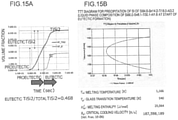
- the method for determining the cooling velocity is as described in Figs. 37 to 39 . By adjusting the cooling velocity to be in the above range, it is possible to fabricate a Si-containing alloy having the microstructure according to an embodiment of the present invention described above.
- a pulverization treatment of the ribbon-like alloy (rapidly quenched ribbon (ribbon) alloy) obtained above is performed.
- proper pulverizing balls for example, zirconia pulverizing balls
- the rapidly quenched ribbon (ribbon) alloy are introduced into a proper pulverizing pot (for example, a zirconia pulverizing pot) and the pulverization treatment is performed at a predetermined number of revolutions for a predetermined time by using a proper pulverizing apparatus (for example, a planetary ball milling apparatus P-6 manufactured by Fritsch GmbH).
- the rapidly quenched ribbon (ribbon) alloy may be previously coarsely pulverized by using a proper pulverizer to a size in which the alloy is easily introduced into the pulverizing apparatus.
- the number of revolutions of the pulverizer maybe, for example, in a range in which the microstructure of alloy formed by the liquid quenching roll solidification method is not impaired, and it is in a range of less than 500 rpm, preferably from 100 to 480 rpm, and more preferably from 300 to 450 rpm.
- the pulverization time may be, for example, in a range in which the microstructure of alloy formed by the liquid quenching roll solidification method is not impaired, and it is in a range of less than 12 hours, preferably from 0.5 to 10 hours, and more preferably from 0.5 to 3 hours.
- the pulverization treatment is usually performed in a dry atmosphere, but the particle size distribution after the pulverization treatment may greatly vary. For this reason, the pulverization treatment and classification treatment for adjusting the particle size may be performed one or more times in combination.
- the ribbon-like alloy (rapidly quenched ribbon (ribbon) alloy) thus obtained may be subjected to a mechanical alloying treatment if necessary.
- a step of pulverizing the rapidly quenched ribbon (ribbon) alloy may be carried out, and the pulverized material thus obtained may be subjected to a mechanical alloying treatment if necessary.
- the mechanical alloying treatment can be performed by a conventionally known method.
- alloying can be achieved by introducing the pulverizing balls and the raw material powders of alloy into the pulverizing pot and increasing the number of revolutions to apply high energy to the materials by using a ball milling apparatus (for example, a planetary ball milling apparatus) .
- the number of revolutions of the ball milling apparatus is, for example, 500 rpm or more and preferably 600 rpm or more.
- the time for the mechanical alloying treatment is, for example, 12 hours or more, preferably 24 hours or more, more preferably 30 hours or more, still more preferably 36 hours or more, particularly preferably 42 hours or more, and most preferably 48 hours or more.
- the upper limit value of the time for the alloying treatment is not particularly set, but it may be usually 72 hours or less.
- the mechanical alloying treatment by the method described above is usually performed in a dry atmosphere, but the particle size distribution after the mechanical alloying treatment may significantly greatly vary in some cases. Hence, it is preferable to perform the pulverization treatment and/or classification treatment for adjusting the particle size.
- the predetermined alloy to be essentially contained in the negative electrode active material layer has been described above, but the negative electrode active material layer may contain other negative electrode active materials.
- the negative electrode active material other than the predetermined alloy may include carbon such as natural graphite, artificial graphite, carbon black, activated carbon, carbon fiber, coke, soft carbon, or hard carbon, a pure metal such as Si or Sn, or an alloy-based active material having a composition ratio which deviates from the predetermined composition ratio described above, or a metal oxide such as TiO, Ti 2 O 3 , or TiO 2 or SiO 2 , SiO, or SnO 2 , a complex oxide of lithium and a transition metal such as Li 4/3 Ti 5/3 O 4 or Li 7 MnN, Li-Pb alloy, Li-Al alloy, or Li.
- the content of the predetermined alloy in 100% by mass of the total amount of the negative electrode active material is preferably from 50 to 100% by mass, more preferably from 80 to 100% by mass, still more preferably from 90 to 100% by mass, particularly preferably from 95 to 100% by mass, and most preferably 100% by mass.
- the microstructure of the Si-containing alloy preferably has a first phase containing a silicide of a transition metal as a main component and a second phase containing Sn and Al in part and amorphous or low crystalline Si as a main component and further has a structure of which a part is composed of a plurality of independent first phases and a part has a eutectic structure composed of the first phase and the second phase as described above.
- the Si phase (second phase) in the eutectic structure is sufficiently amorphized.
- the critical cooling velocity, the liquidus temperature, the T 0 curve, the glass transition temperature, the crystallization temperature and the like are used as a specific index of amorphous phase forming ability.
- amorphous phase forming ability can be compared by the critical cooling velocity even in a case in which the alloy systems are different from one another.
- the critical cooling velocity is the lowest cooling velocity at which an atom or a molecule forms an amorphous phase . It is possible to produce an alloy having an amorphous phase by setting the cooling velocity in the production of the alloy to be equal to or higher than the critical cooling velocity. In other words, an alloy composition having a slow critical cooling velocity is considered to have high amorphous phase forming ability since it can be amorphized even when being slowly cooled.
- the critical cooling velocity F of the liquid phase composition at the start of eutectic formation in the mother alloy composition is 3.2 ⁇ 10 8 K/sec or less, preferably 3.0 ⁇ 10 8 K/sec or less from the viewpoint of sufficiently amorphizing the second phase in the eutectic structure.
- the critical cooling velocity F is more preferably 2.8 ⁇ 10 8 K/sec or less, still more preferably 2.7 ⁇ 10 8 K/sec or less, and particularly preferably 2.6 ⁇ 10 8 K/sec or less.
- the lower limit of the critical cooling velocity F is not particularly limited, and it is, for example, 4.0 ⁇ 10 7 K/sec or more.
- the critical cooling velocity of the liquid phase composition at the start of eutectic formation in the alloy composition will be described by taking the alloy composition used in Example 1 as an example.
- the critical cooling velocity of the liquid phase composition at the start of eutectic formation can be determined by the same method.
- the Scheil solidification simulation of the Si-Al-Ti ternary alloy of Example 1 was performed using the Scheil model, the integrated thermodynamic calculation system: Thermo-Calc Ver2015a developed by Thermo-Calc software AB Sweden (Japan Agency: Itochu Techno-Solutions Corporation) and solid solution general purpose database: SSOL5 (SGTE* Solution Database, ver.5.0) as a thermodynamic database.
- the Scheil model and the Scheil solidification simulation are performed in conformity to Metal vol. 77, No. 8 (p.898 to p.904 ) .
- the liquid phase composition at the start of eutectic formation in the alloy composition can be determined by the Scheil solidification simulation.
- the structure is composed of a proeutectic silicide (TiSi 2 ) and a eutectic (TiSi 2 + Si) and there are a small number of Si phases and Al single phases.
- the precipitated phase is a silicide (TiSi 2 ) phase and a Si phase.
- the composition of the solid phase is considered to be constant regardless of the temperature, and it is thus considered that the actual state is well reproduced even when such Scheil model is used.
- Equation (1) volume fraction of crystals generated at the retention time: t: X, nucleation frequency: I, and nucleation rate: U
- Equation (2) volume fraction of crystals generated at the retention time: t: X, nucleation frequency: I, and nucleation rate: U
- G m denotes the driving force for crystallizing a crystal from a liquid phase
- G ⁇ denotes the free energy for generating a spherical crystal nucleus from a liquid phase
- ⁇ denotes the viscosity coefficient
- N v denotes the number of atoms per unit volume.
- G ⁇ can be expressed as ⁇ m (solid-liquid interface energy) by the following Equation (3).
- G m can be approximated by the following Equation (4).
- ⁇ m is empirically expressed as the following Equation (5) and is indicated to be about 0.41 by Saunders and Miodownik.
- Equation (6) denotes the proportion of sites at which atoms can move at the solid-liquid interface and is expressed as the following Equation (6) according to Uhlmann.
- the viscosity coefficient ⁇ of the liquid alloy can be approximated by the Doolittle equation (following Equation (7)).
- A, B and C denote constants.
- f T denotes the relative free volume in the liquid
- E H denotes the void formation energy.
- T g glass transition temperature
- the composition at the start of eutectic formation was determined by the Scheil solidification simulation described above, then the glass transition temperature, the liquidus temperature and the melting enthalpy were determined, the TTT diagram ( Fig. 45 ) was calculated by Equation (2) above, and the critical cooling velocity R c was calculated by the following Equation (9).
- the TTT diagram for the alloy composition of Example 1 is illustrated in Fig. 15(b) .
- the critical cooling velocity is calculated to be 1.39E + 08 K/sec in the alloy composition of Example 1.
- the critical cooling velocity F of the liquid phase composition at the start of eutectic formation in the mother alloy composition of the Si-containing alloy and the ratio E of a silicide of a transition metal in the eutectic structure to silicides of all transition metals in the rapidly quenched ribbon of the Si-containing alloy satisfy preferably E/F > 1.7 ⁇ 10 -9 sec/K, more preferably E/F > 2.2 ⁇ 10 -9 sec/K, and still more preferably E/F> 2.3 ⁇ 10 -9 sec/K.
- the upper limit of the E/F is not particularly limited as long as the range of the critical cooling velocity F described above and the range of the ratio F to be described below are satisfied.
- the critical cooling velocity F of the liquid phase composition at the start of eutectic formation in the mother alloy composition of the Si-containing alloy is slow from the viewpoint of amorphous phase forming ability.
- a silicide of a transition metal (first phase) exists in the eutectic structure in a larger amount from the viewpoint of suppressing expansion of the a-Si phase (second phase) in the eutectic structure in the charge and discharge process.
- the ratio E of a silicide of a transition metal in the eutectic structure to silicides of all transition metals in the rapidly quenched ribbon of the Si-containing alloy can be calculated by the precipitation calculation described above.
- Fig. 15(a) is a graph illustrating the results on the precipitation simulation of TiSi 2 and Si in Example 1.
- the vertical axis represents the volume fraction and the horizontal axis represents the time.
- Fig. 15(a) illustrates that silicide (TiSi 2 ) crystallizes as a proeutectic and then Si crystallizes.
- TiSi 2 crystallizes as a proeutectic until Si crystallizes and TiSi 2 and Si form a eutectic after Si is crystallized.
- the ratio E of a silicide of a transition metal in the eutectic structure to silicides of all transition metals in the rapidly quenched ribbon of the Si-containing alloy can be calculated.
- the same as the above can be said from Figs. 19(a) , 22(a) , 24(a) , 26(a) , 28(a) , 30(a) , and 32(a) , which illustrate the results on the same precipitation simulation, and the ratio E described above can be calculated (see the respective drawings and Table 1).
- the ratio E of a silicide of a transition metal in the eutectic structure to silicides of all transition metals is preferably 0.3 or more, more preferably 0.35 or more, still more preferably 0.4 or more, and yet more preferably 0.43 or more from the viewpoint of suppressing expansion of the a-Si phase (second phase) in the eutectic structure in the charge and discharge process.
- the upper limit of the ratio E is not particularly limited, but it is, for example, 0.8 or less and preferably 0.7 or less.
- the negative electrode active material layer 13 contains a binder.
- a binder is added for the purpose of binding the active materials with each other or the active material with the current collector and thus maintaining the electrode structure.
- the kind of binder to be used in the negative electrode active material layer is also not particularly limited, and those described above as the binder to be used in the positive electrode active material layer can be used in the same manner. Hence, the detailed description thereon will be omitted here.
- the amount of the binder to be contained in the negative electrode active material layer is not particularly limited as long as it is an amount in which the active material can be bound, but it is preferably from 0.5% to 20% by mass and more preferably from 1% to 15% by mass with respect to the negative electrode active material layer.
- the positive electrode active material layer 15 and the negative electrode active material layer 13 contain a conductive auxiliary, an electrolyte salt (lithium salt), an ion conductive polymer, and the like if necessary.
- the negative electrode active material layer 13 essentially contains a conductive auxiliary as well.
- the conductive auxiliary refers to an additive to be compounded for improving the electrical conductivity of the positive electrode active material layer or the negative electrode active material layer.
- Examples of the conductive auxiliary may include carbon materials such as carbon black such as acetylene black, graphite, and a vapor-grown carbon fiber.
- the electronic network inside the active material layer is effectively formed when the active material layer contains a conductive auxiliary, and this can contribute to the improvement in output characteristics of the battery.
- the content of the conductive auxiliary to be mixed in the active material layer is in a range of 1% by mass or more, more preferably 3% by mass or more, and still more preferably 5% by mass or more with respect to the total amount of the active material layer.
- the content of the conductive auxiliary to be mixed in the active material layer is in a range of preferably 15% by mass or less, more preferably 10% by mass or less, still more preferably 7% by mass or less with respect to the total amount of the active material layer.
- the electron conductivity of the active material itself is low, the electrode resistance can be decreased depending on the amount of the conductive auxiliary, and the following effects are exerted by regulating the compounding ratio (content) of the conductive auxiliary in the active material layer to be in the above range. In other words, it is possible to sufficiently ensure the electron conductivity without hindering the electrode reaction, to suppress a decrease in energy density due to a decrease in electrode density, and thus to attain the improvement in energy density due to the improvement in electrode density.
- a conductive binder having the functions of both a conductive auxiliary and a binder may be used instead of these conductive auxiliary and binder or may be concurrently used with one or both of these conductive auxiliary and binder.
- the conductive binder commercially available TAB-2 (manufactured by Hohsen Corp.) can be used.
- Examples of the electrolyte salt may include Li(C 2 F 5 SO 2 ) 2 N, LiPF 6 , LiBF 4 , LiClO 4 , LiAsF 6 , and LiCF 3 SO 3 .
- nonconductive polymer material may include polyethylene (PE; high density polyethylene (HDPE), low density polyethylene (LDPE), and the like), polypropylene (PP), polyethylene terephthalate (PET), polyether nitrile (PEN), polyimide (PI), polyamide-imide (PAI), polyamide (PA), polytetrafluoroethylene (PTFE), styrene-butadiene rubber (SBR), polyacrylonitrile (PAN), polymethyl acrylate (PMA), polymethyl methacrylate (PMMA), polyvinyl chloride (PVC), polyvinylidene fluoride (PVdF), or polystyrene (PS) .
- PE polyethylene
- HDPE high density polyethylene
- LDPE low density polyethylene
- PP polypropylene
- PET polyethylene terephthalate
- PEN polyether nitrile
- PI polyimide
- PAI polyamide-imide
- PA polyamide
- PA polytetrafluoroethylene
- the lithium ion batteries in which the negative electrode active material according to the present invention is used exhibit excellent cycle durability as the discharge capacity retention after 50 cycles is maintained at a high value.
- the capacity is higher in Examples in which the Si-containing alloy negative electrode is used than in a negative electrode active material in which a carbon material is used (the corresponding Comparative Example is omitted since this fact is known so much (see the background art) and there is no need to show Comparative Example using a negative electrode material).
Landscapes
- Chemical & Material Sciences (AREA)
- Chemical Kinetics & Catalysis (AREA)
- Electrochemistry (AREA)
- General Chemical & Material Sciences (AREA)
- Engineering & Computer Science (AREA)
- Materials Engineering (AREA)
- Mechanical Engineering (AREA)
- Metallurgy (AREA)
- Organic Chemistry (AREA)
- Battery Electrode And Active Subsutance (AREA)
- Electric Double-Layer Capacitors Or The Like (AREA)
Claims (14)
- Matériau actif d'électrode négative pour dispositif électrique, comprenant un alliage de Si dont la composition est représentée par la formule chimique suivante (1) :
[formule chimique 1]
SixSnyMzAlwAa (1)
dans lequel, dans la formule chimique (1) ci-avant,M représente un, deux ou plusieurs éléments métalliques de transition sélectionnés parmi le groupe constitué par Ti, Zr, Ni, Cu, Mo, Nb, Sc, Co, Cr et Fe,A représente les impuretés inévitables, etx, y, z, w et a représentent des valeurs en pourcentage massique, dans lequel y, z et w sont respectivement 2 ≤ y ≤ 10, 25 ≤ z ≤ 35 et 0,3 ≤ w ≤ 3, et x + y + z + w + a = 100. - Matériau actif d'électrode négative pour dispositif électrique selon la revendication 1, dans lequel le ratio atomique de Sn par Al dans l'alliage de Si est compris entre 0,3:1 à 3:1.
- Matériau actif d'électrode négative pour dispositif électrique selon la revendication 1 ou 2, dans lequel une microstructure de l'alliage de Si présente une première phase contenant un siliciure d'un métal de transition comme composant principal et une deuxième phase contenant du Sn et de l'Al en partie et du Si amorphe ou faiblement cristallin comme composant principal, et présente en outre une structure dont une partie est composée d'une pluralité des premières phases qui sont indépendantes et une partie a une structure eutectique composée de la première phase et de la deuxième phase.
- Matériau actif d'électrode négative pour dispositif électrique selon la revendication 3, dans lequel un rayon modal A des premières phases qui sont indépendantes dans la microstructure est inférieur ou égal à 250 nm.
- Matériau actif d'électrode négative pour dispositif électrique selon l'une quelconque des revendications 3 et 4, dans lequel le ratio D2 du rayon modal A des premières phases qui sont indépendantes par le rayon modal C des deuxièmes phases de la structure eutectique dans la microstructure (rayon modal A des premières phases qui sont indépendantes / rayon modal C des deuxièmes phases de la structure eutectique) est inférieur ou égal à 4,5.
- Matériau actif d'électrode négative pour dispositif électrique selon l'une quelconque des revendications 3 à 5, dans lequel le ratio D3 du rayon modal B des premières phases par le rayon modal C des deuxièmes phases dans la structure eutectique (rayon modal B des premières phases de la structure eutectique / rayon modal C des deuxièmes phases de la structure eutectique) est inférieur ou égal à 1.
- Matériau actif d'électrode négative pour dispositif électrique selon l'une quelconque des revendications 1 à 6, dans lequel M est du Ti.
- Matériau actif d'électrode négative pour dispositif électrique selon l'une quelconque des revendications 1 à 7, dans lequel a est inférieur à 0,5 pour cent en masse.
- Matériau actif d'électrode négative pour dispositif électrique selon l'une quelconque des revendications 1 à 8, dans lequel a est inférieur à 0,1 pour cent en masse.
- Procédé de production du matériau actif d'électrode négative pour dispositif électrique selon l'une quelconque des revendications 1 à 9, le procédé comprenant la fabrication d'un ruban rapidement trempé d'un alliage de Si en utilisant un alliage mère présentant la même composition que celle de l'alliage de Si selon un procédé de solidification par trempe liquide.
- Procédé de production selon la revendication 10, dans lequel la vitesse de refroidissement critique F de la composition en phase liquide au début de la formation eutectique dans la composition d'alliage mère est inférieure ou égale à 3 × 10⁸ K/sec.
- Procédé de production selon la revendication 11, dans lequel la vitesse de refroidissement critique F et un ratio E du siliciure d'un métal de transition dans la structure eutectique par le siliciure de tous les métaux de transition dans le ruban rapidement trempé dans l'alliage de Si répond à la condition E/F > 2,2 × 10⁻⁹ sec/K.
- Électrode négative pour dispositif électrique, comprenant le matériau actif d'électrode négative pour dispositif électrique selon l'une quelconque des revendications 1 à 9.
- Dispositif électrique comprenant l'électrode négative pour dispositif électrique selon la revendication 13.
Applications Claiming Priority (1)
| Application Number | Priority Date | Filing Date | Title |
|---|---|---|---|
| PCT/JP2016/068017 WO2017216940A1 (fr) | 2016-06-16 | 2016-06-16 | Matériau actif d'électrode négative pour dispositif électrique, et dispositif électrique dans lequel ledit matériau est utilisé |
Publications (3)
| Publication Number | Publication Date |
|---|---|
| EP3474355A1 EP3474355A1 (fr) | 2019-04-24 |
| EP3474355A4 EP3474355A4 (fr) | 2019-07-03 |
| EP3474355B1 true EP3474355B1 (fr) | 2022-02-16 |
Family
ID=60664024
Family Applications (1)
| Application Number | Title | Priority Date | Filing Date |
|---|---|---|---|
| EP16905495.4A Active EP3474355B1 (fr) | 2016-06-16 | 2016-06-16 | Matériau actif d'électrode négative pour dispositif électrique, et dispositif électrique dans lequel ledit matériau est utilisé |
Country Status (6)
| Country | Link |
|---|---|
| US (1) | US10840506B2 (fr) |
| EP (1) | EP3474355B1 (fr) |
| JP (1) | JP6760373B2 (fr) |
| CN (1) | CN109314233B (fr) |
| MY (1) | MY196415A (fr) |
| WO (1) | WO2017216940A1 (fr) |
Families Citing this family (1)
| Publication number | Priority date | Publication date | Assignee | Title |
|---|---|---|---|---|
| JP7813688B2 (ja) * | 2021-10-06 | 2026-02-13 | カナデビア株式会社 | アルミニウム合金における添加元素固溶量の予測方法、供試材の作製方法およびこれを使用する強度評価方法 |
Citations (1)
| Publication number | Priority date | Publication date | Assignee | Title |
|---|---|---|---|---|
| US20150303451A1 (en) * | 2012-11-22 | 2015-10-22 | Nissan Motor Co., Ltd. | Negative electrode for electric device and electric device using the same |
Family Cites Families (14)
| Publication number | Priority date | Publication date | Assignee | Title |
|---|---|---|---|---|
| JP2001297757A (ja) | 2000-04-14 | 2001-10-26 | Sumitomo Metal Ind Ltd | 非水電解質二次電池用負極材料およびその製造方法 |
| KR100721500B1 (ko) | 2003-03-26 | 2007-05-23 | 캐논 가부시끼가이샤 | 리튬2차전지용의 전극재료 및 이 전극재료를 가진전극구조체 |
| JP4464173B2 (ja) | 2003-03-26 | 2010-05-19 | キヤノン株式会社 | リチウム二次電池用の電極材料、該電極材料を有する電極構造体、及び該電極構造体を有する二次電池 |
| CN100533821C (zh) | 2005-06-03 | 2009-08-26 | 松下电器产业株式会社 | 非水电解质二次电池及其负极的制备方法 |
| US7851085B2 (en) * | 2005-07-25 | 2010-12-14 | 3M Innovative Properties Company | Alloy compositions for lithium ion batteries |
| EP2239803A1 (fr) * | 2009-04-10 | 2010-10-13 | Saft Groupe Sa | Composition de matiere active pour electrode negative d'accumulateur lithium-ion. |
| JP2012038708A (ja) * | 2010-07-16 | 2012-02-23 | Sanyo Special Steel Co Ltd | 導電性に優れるSi系合金負極材料およびその製造方法 |
| JP5766445B2 (ja) | 2011-01-17 | 2015-08-19 | 山陽特殊製鋼株式会社 | リチウムイオン二次電池負極用Si合金粉末およびその製造方法 |
| JP5904363B2 (ja) | 2011-12-27 | 2016-04-13 | 日産自動車株式会社 | 電気デバイス用負極活物質 |
| JP6322362B2 (ja) | 2012-02-01 | 2018-05-09 | 山陽特殊製鋼株式会社 | Si系合金負極材料 |
| WO2014034494A1 (fr) * | 2012-08-31 | 2014-03-06 | 中央電気工業株式会社 | Particules d'alliage, électrode, accumulateur à électrolyte non aqueux et procédé de production de particules d'alliage |
| US20150303450A1 (en) * | 2012-11-22 | 2015-10-22 | Nissan Motor Co., Ltd. | Negative electrode for electrical device, and electrical device using the same |
| CN105308777B (zh) * | 2013-06-12 | 2017-08-08 | 日产自动车株式会社 | 电气设备用负极活性物质、及使用其的电气设备 |
| KR101775542B1 (ko) * | 2013-08-20 | 2017-09-06 | 삼성에스디아이 주식회사 | 리튬 이차 전지용 음극 활물질, 이의 제조 방법, 그리고 이를 포함하는 음극 및 리튬 이차 전지 |
-
2016
- 2016-06-16 JP JP2018523131A patent/JP6760373B2/ja active Active
- 2016-06-16 US US16/309,848 patent/US10840506B2/en active Active
- 2016-06-16 MY MYPI2018002574A patent/MY196415A/en unknown
- 2016-06-16 WO PCT/JP2016/068017 patent/WO2017216940A1/fr not_active Ceased
- 2016-06-16 CN CN201680086832.7A patent/CN109314233B/zh active Active
- 2016-06-16 EP EP16905495.4A patent/EP3474355B1/fr active Active
Patent Citations (1)
| Publication number | Priority date | Publication date | Assignee | Title |
|---|---|---|---|---|
| US20150303451A1 (en) * | 2012-11-22 | 2015-10-22 | Nissan Motor Co., Ltd. | Negative electrode for electric device and electric device using the same |
Also Published As
| Publication number | Publication date |
|---|---|
| MY196415A (en) | 2023-03-29 |
| JPWO2017216940A1 (ja) | 2019-04-11 |
| US20190173081A1 (en) | 2019-06-06 |
| EP3474355A4 (fr) | 2019-07-03 |
| JP6760373B2 (ja) | 2020-09-23 |
| EP3474355A1 (fr) | 2019-04-24 |
| CN109314233B (zh) | 2020-08-11 |
| US10840506B2 (en) | 2020-11-17 |
| WO2017216940A1 (fr) | 2017-12-21 |
| CN109314233A (zh) | 2019-02-05 |
Similar Documents
| Publication | Publication Date | Title |
|---|---|---|
| JP6798411B2 (ja) | 電気デバイス用負極活物質、およびこれを用いた電気デバイス | |
| EP3376571B1 (fr) | Matériau actif d'électrode négative pour dispositif électrique, et dispositif électrique l'utilisant | |
| EP3236520B1 (fr) | Matériau actif d'électrode négative pour un dispositif électrique et dispositif électrique l'utilisant | |
| EP3236518B1 (fr) | Matériau actif d'électrode négative pour batterie secondaire lithium-ion et batterie secondaire lithium-ion l'utilisant | |
| KR20150082516A (ko) | 전기 디바이스용 부극, 및 이것을 사용한 전기 디바이스 | |
| EP3376570B1 (fr) | Matériau actif d'électrode négative pour dispositif électrique, et dispositif électrique utilisant ledit matériau | |
| EP3236515B1 (fr) | Matière active d'électrode négative pour dispositif électrique et dispositif électrique l'utilisant | |
| JP6705302B2 (ja) | 電気デバイス用負極活物質、およびこれを用いた電気デバイス | |
| EP3236516B1 (fr) | Matière active d'électrode négative pour dispositif électrique et dispositif électrique l'utilisant | |
| US10840506B2 (en) | Negative electrode active material for electrical device and electrical device using the same | |
| EP3680967B1 (fr) | Matériau actif d'électrode négative pour dispositifs électriques, son procédé de production, et dispositif électrique utilisant ce matériau actif |
Legal Events
| Date | Code | Title | Description |
|---|---|---|---|
| STAA | Information on the status of an ep patent application or granted ep patent |
Free format text: STATUS: THE INTERNATIONAL PUBLICATION HAS BEEN MADE |
|
| PUAI | Public reference made under article 153(3) epc to a published international application that has entered the european phase |
Free format text: ORIGINAL CODE: 0009012 |
|
| STAA | Information on the status of an ep patent application or granted ep patent |
Free format text: STATUS: REQUEST FOR EXAMINATION WAS MADE |
|
| 17P | Request for examination filed |
Effective date: 20181214 |
|
| AK | Designated contracting states |
Kind code of ref document: A1 Designated state(s): AL AT BE BG CH CY CZ DE DK EE ES FI FR GB GR HR HU IE IS IT LI LT LU LV MC MK MT NL NO PL PT RO RS SE SI SK SM TR |
|
| AX | Request for extension of the european patent |
Extension state: BA ME |
|
| A4 | Supplementary search report drawn up and despatched |
Effective date: 20190531 |
|
| RIC1 | Information provided on ipc code assigned before grant |
Ipc: C01B 33/06 20060101ALI20190524BHEP Ipc: C22C 28/00 20060101ALI20190524BHEP Ipc: H01M 4/38 20060101AFI20190524BHEP |
|
| DAV | Request for validation of the european patent (deleted) | ||
| DAX | Request for extension of the european patent (deleted) | ||
| STAA | Information on the status of an ep patent application or granted ep patent |
Free format text: STATUS: EXAMINATION IS IN PROGRESS |
|
| 17Q | First examination report despatched |
Effective date: 20200210 |
|
| RIC1 | Information provided on ipc code assigned before grant |
Ipc: H01M 10/0525 20100101ALI20210621BHEP Ipc: H01M 4/134 20100101ALI20210621BHEP Ipc: C01B 33/06 20060101ALI20210621BHEP Ipc: C22C 28/00 20060101ALI20210621BHEP Ipc: H01M 4/38 20060101AFI20210621BHEP |
|
| GRAP | Despatch of communication of intention to grant a patent |
Free format text: ORIGINAL CODE: EPIDOSNIGR1 |
|
| STAA | Information on the status of an ep patent application or granted ep patent |
Free format text: STATUS: GRANT OF PATENT IS INTENDED |
|
| INTG | Intention to grant announced |
Effective date: 20210902 |
|
| RIN1 | Information on inventor provided before grant (corrected) |
Inventor name: WATANABE, MANABU Inventor name: YOSHIOKA, YOUICHI Inventor name: CHIBA, NOBUTAKA Inventor name: ARAI, MASAYA |
|
| GRAS | Grant fee paid |
Free format text: ORIGINAL CODE: EPIDOSNIGR3 |
|
| GRAA | (expected) grant |
Free format text: ORIGINAL CODE: 0009210 |
|
| STAA | Information on the status of an ep patent application or granted ep patent |
Free format text: STATUS: THE PATENT HAS BEEN GRANTED |
|
| AK | Designated contracting states |
Kind code of ref document: B1 Designated state(s): AL AT BE BG CH CY CZ DE DK EE ES FI FR GB GR HR HU IE IS IT LI LT LU LV MC MK MT NL NO PL PT RO RS SE SI SK SM TR |
|
| REG | Reference to a national code |
Ref country code: GB Ref legal event code: FG4D |
|
| REG | Reference to a national code |
Ref country code: CH Ref legal event code: EP |
|
| REG | Reference to a national code |
Ref country code: DE Ref legal event code: R096 Ref document number: 602016069261 Country of ref document: DE |
|
| REG | Reference to a national code |
Ref country code: AT Ref legal event code: REF Ref document number: 1469455 Country of ref document: AT Kind code of ref document: T Effective date: 20220315 |
|
| REG | Reference to a national code |
Ref country code: IE Ref legal event code: FG4D |
|
| REG | Reference to a national code |
Ref country code: LT Ref legal event code: MG9D |
|
| REG | Reference to a national code |
Ref country code: NL Ref legal event code: MP Effective date: 20220216 |
|
| REG | Reference to a national code |
Ref country code: AT Ref legal event code: MK05 Ref document number: 1469455 Country of ref document: AT Kind code of ref document: T Effective date: 20220216 |
|
| PG25 | Lapsed in a contracting state [announced via postgrant information from national office to epo] |
Ref country code: SE Free format text: LAPSE BECAUSE OF FAILURE TO SUBMIT A TRANSLATION OF THE DESCRIPTION OR TO PAY THE FEE WITHIN THE PRESCRIBED TIME-LIMIT Effective date: 20220216 Ref country code: RS Free format text: LAPSE BECAUSE OF FAILURE TO SUBMIT A TRANSLATION OF THE DESCRIPTION OR TO PAY THE FEE WITHIN THE PRESCRIBED TIME-LIMIT Effective date: 20220216 Ref country code: PT Free format text: LAPSE BECAUSE OF FAILURE TO SUBMIT A TRANSLATION OF THE DESCRIPTION OR TO PAY THE FEE WITHIN THE PRESCRIBED TIME-LIMIT Effective date: 20220616 Ref country code: NO Free format text: LAPSE BECAUSE OF FAILURE TO SUBMIT A TRANSLATION OF THE DESCRIPTION OR TO PAY THE FEE WITHIN THE PRESCRIBED TIME-LIMIT Effective date: 20220516 Ref country code: NL Free format text: LAPSE BECAUSE OF FAILURE TO SUBMIT A TRANSLATION OF THE DESCRIPTION OR TO PAY THE FEE WITHIN THE PRESCRIBED TIME-LIMIT Effective date: 20220216 Ref country code: LT Free format text: LAPSE BECAUSE OF FAILURE TO SUBMIT A TRANSLATION OF THE DESCRIPTION OR TO PAY THE FEE WITHIN THE PRESCRIBED TIME-LIMIT Effective date: 20220216 Ref country code: HR Free format text: LAPSE BECAUSE OF FAILURE TO SUBMIT A TRANSLATION OF THE DESCRIPTION OR TO PAY THE FEE WITHIN THE PRESCRIBED TIME-LIMIT Effective date: 20220216 Ref country code: ES Free format text: LAPSE BECAUSE OF FAILURE TO SUBMIT A TRANSLATION OF THE DESCRIPTION OR TO PAY THE FEE WITHIN THE PRESCRIBED TIME-LIMIT Effective date: 20220216 Ref country code: BG Free format text: LAPSE BECAUSE OF FAILURE TO SUBMIT A TRANSLATION OF THE DESCRIPTION OR TO PAY THE FEE WITHIN THE PRESCRIBED TIME-LIMIT Effective date: 20220516 |
|
| PG25 | Lapsed in a contracting state [announced via postgrant information from national office to epo] |
Ref country code: PL Free format text: LAPSE BECAUSE OF FAILURE TO SUBMIT A TRANSLATION OF THE DESCRIPTION OR TO PAY THE FEE WITHIN THE PRESCRIBED TIME-LIMIT Effective date: 20220216 Ref country code: LV Free format text: LAPSE BECAUSE OF FAILURE TO SUBMIT A TRANSLATION OF THE DESCRIPTION OR TO PAY THE FEE WITHIN THE PRESCRIBED TIME-LIMIT Effective date: 20220216 Ref country code: GR Free format text: LAPSE BECAUSE OF FAILURE TO SUBMIT A TRANSLATION OF THE DESCRIPTION OR TO PAY THE FEE WITHIN THE PRESCRIBED TIME-LIMIT Effective date: 20220517 Ref country code: FI Free format text: LAPSE BECAUSE OF FAILURE TO SUBMIT A TRANSLATION OF THE DESCRIPTION OR TO PAY THE FEE WITHIN THE PRESCRIBED TIME-LIMIT Effective date: 20220216 Ref country code: AT Free format text: LAPSE BECAUSE OF FAILURE TO SUBMIT A TRANSLATION OF THE DESCRIPTION OR TO PAY THE FEE WITHIN THE PRESCRIBED TIME-LIMIT Effective date: 20220216 |
|
| PG25 | Lapsed in a contracting state [announced via postgrant information from national office to epo] |
Ref country code: IS Free format text: LAPSE BECAUSE OF FAILURE TO SUBMIT A TRANSLATION OF THE DESCRIPTION OR TO PAY THE FEE WITHIN THE PRESCRIBED TIME-LIMIT Effective date: 20220617 |
|
| PG25 | Lapsed in a contracting state [announced via postgrant information from national office to epo] |
Ref country code: SM Free format text: LAPSE BECAUSE OF FAILURE TO SUBMIT A TRANSLATION OF THE DESCRIPTION OR TO PAY THE FEE WITHIN THE PRESCRIBED TIME-LIMIT Effective date: 20220216 Ref country code: SK Free format text: LAPSE BECAUSE OF FAILURE TO SUBMIT A TRANSLATION OF THE DESCRIPTION OR TO PAY THE FEE WITHIN THE PRESCRIBED TIME-LIMIT Effective date: 20220216 Ref country code: RO Free format text: LAPSE BECAUSE OF FAILURE TO SUBMIT A TRANSLATION OF THE DESCRIPTION OR TO PAY THE FEE WITHIN THE PRESCRIBED TIME-LIMIT Effective date: 20220216 Ref country code: EE Free format text: LAPSE BECAUSE OF FAILURE TO SUBMIT A TRANSLATION OF THE DESCRIPTION OR TO PAY THE FEE WITHIN THE PRESCRIBED TIME-LIMIT Effective date: 20220216 Ref country code: DK Free format text: LAPSE BECAUSE OF FAILURE TO SUBMIT A TRANSLATION OF THE DESCRIPTION OR TO PAY THE FEE WITHIN THE PRESCRIBED TIME-LIMIT Effective date: 20220216 Ref country code: CZ Free format text: LAPSE BECAUSE OF FAILURE TO SUBMIT A TRANSLATION OF THE DESCRIPTION OR TO PAY THE FEE WITHIN THE PRESCRIBED TIME-LIMIT Effective date: 20220216 |
|
| REG | Reference to a national code |
Ref country code: DE Ref legal event code: R097 Ref document number: 602016069261 Country of ref document: DE |
|
| PG25 | Lapsed in a contracting state [announced via postgrant information from national office to epo] |
Ref country code: AL Free format text: LAPSE BECAUSE OF FAILURE TO SUBMIT A TRANSLATION OF THE DESCRIPTION OR TO PAY THE FEE WITHIN THE PRESCRIBED TIME-LIMIT Effective date: 20220216 |
|
| PLBE | No opposition filed within time limit |
Free format text: ORIGINAL CODE: 0009261 |
|
| STAA | Information on the status of an ep patent application or granted ep patent |
Free format text: STATUS: NO OPPOSITION FILED WITHIN TIME LIMIT |
|
| 26N | No opposition filed |
Effective date: 20221117 |
|
| PG25 | Lapsed in a contracting state [announced via postgrant information from national office to epo] |
Ref country code: MC Free format text: LAPSE BECAUSE OF FAILURE TO SUBMIT A TRANSLATION OF THE DESCRIPTION OR TO PAY THE FEE WITHIN THE PRESCRIBED TIME-LIMIT Effective date: 20220216 |
|
| REG | Reference to a national code |
Ref country code: CH Ref legal event code: PL |
|
| REG | Reference to a national code |
Ref country code: BE Ref legal event code: MM Effective date: 20220630 |
|
| PG25 | Lapsed in a contracting state [announced via postgrant information from national office to epo] |
Ref country code: SI Free format text: LAPSE BECAUSE OF FAILURE TO SUBMIT A TRANSLATION OF THE DESCRIPTION OR TO PAY THE FEE WITHIN THE PRESCRIBED TIME-LIMIT Effective date: 20220216 |
|
| PG25 | Lapsed in a contracting state [announced via postgrant information from national office to epo] |
Ref country code: LU Free format text: LAPSE BECAUSE OF NON-PAYMENT OF DUE FEES Effective date: 20220616 Ref country code: LI Free format text: LAPSE BECAUSE OF NON-PAYMENT OF DUE FEES Effective date: 20220630 Ref country code: IE Free format text: LAPSE BECAUSE OF NON-PAYMENT OF DUE FEES Effective date: 20220616 Ref country code: CH Free format text: LAPSE BECAUSE OF NON-PAYMENT OF DUE FEES Effective date: 20220630 |
|
| PG25 | Lapsed in a contracting state [announced via postgrant information from national office to epo] |
Ref country code: BE Free format text: LAPSE BECAUSE OF NON-PAYMENT OF DUE FEES Effective date: 20220630 |
|
| PG25 | Lapsed in a contracting state [announced via postgrant information from national office to epo] |
Ref country code: IT Free format text: LAPSE BECAUSE OF FAILURE TO SUBMIT A TRANSLATION OF THE DESCRIPTION OR TO PAY THE FEE WITHIN THE PRESCRIBED TIME-LIMIT Effective date: 20220216 |
|
| PG25 | Lapsed in a contracting state [announced via postgrant information from national office to epo] |
Ref country code: HU Free format text: LAPSE BECAUSE OF FAILURE TO SUBMIT A TRANSLATION OF THE DESCRIPTION OR TO PAY THE FEE WITHIN THE PRESCRIBED TIME-LIMIT; INVALID AB INITIO Effective date: 20160616 |
|
| PG25 | Lapsed in a contracting state [announced via postgrant information from national office to epo] |
Ref country code: MK Free format text: LAPSE BECAUSE OF FAILURE TO SUBMIT A TRANSLATION OF THE DESCRIPTION OR TO PAY THE FEE WITHIN THE PRESCRIBED TIME-LIMIT Effective date: 20220216 Ref country code: CY Free format text: LAPSE BECAUSE OF FAILURE TO SUBMIT A TRANSLATION OF THE DESCRIPTION OR TO PAY THE FEE WITHIN THE PRESCRIBED TIME-LIMIT Effective date: 20220216 |
|
| PG25 | Lapsed in a contracting state [announced via postgrant information from national office to epo] |
Ref country code: MT Free format text: LAPSE BECAUSE OF FAILURE TO SUBMIT A TRANSLATION OF THE DESCRIPTION OR TO PAY THE FEE WITHIN THE PRESCRIBED TIME-LIMIT Effective date: 20220216 |
|
| PGFP | Annual fee paid to national office [announced via postgrant information from national office to epo] |
Ref country code: DE Payment date: 20250520 Year of fee payment: 10 |
|
| PGFP | Annual fee paid to national office [announced via postgrant information from national office to epo] |
Ref country code: GB Payment date: 20250520 Year of fee payment: 10 |
|
| PGFP | Annual fee paid to national office [announced via postgrant information from national office to epo] |
Ref country code: FR Payment date: 20250520 Year of fee payment: 10 |
|
| PG25 | Lapsed in a contracting state [announced via postgrant information from national office to epo] |
Ref country code: TR Free format text: LAPSE BECAUSE OF FAILURE TO SUBMIT A TRANSLATION OF THE DESCRIPTION OR TO PAY THE FEE WITHIN THE PRESCRIBED TIME-LIMIT Effective date: 20220216 |