EP3475882B1 - Integrierte schaltungsmodule und chipkarten damit - Google Patents
Integrierte schaltungsmodule und chipkarten damit Download PDFInfo
- Publication number
- EP3475882B1 EP3475882B1 EP18755387.0A EP18755387A EP3475882B1 EP 3475882 B1 EP3475882 B1 EP 3475882B1 EP 18755387 A EP18755387 A EP 18755387A EP 3475882 B1 EP3475882 B1 EP 3475882B1
- Authority
- EP
- European Patent Office
- Prior art keywords
- pair
- contact pads
- module
- aperture
- bond
- Prior art date
- Legal status (The legal status is an assumption and is not a legal conclusion. Google has not performed a legal analysis and makes no representation as to the accuracy of the status listed.)
- Active
Links
Images







Classifications
-
- H—ELECTRICITY
- H10—SEMICONDUCTOR DEVICES; ELECTRIC SOLID-STATE DEVICES NOT OTHERWISE PROVIDED FOR
- H10F—INORGANIC SEMICONDUCTOR DEVICES SENSITIVE TO INFRARED RADIATION, LIGHT, ELECTROMAGNETIC RADIATION OF SHORTER WAVELENGTH OR CORPUSCULAR RADIATION
- H10F39/00—Integrated devices, or assemblies of multiple devices, comprising at least one element covered by group H10F30/00, e.g. radiation detectors comprising photodiode arrays
- H10F39/10—Integrated devices
- H10F39/12—Image sensors
- H10F39/198—Contact-type image sensors [CIS]
-
- G—PHYSICS
- G06—COMPUTING OR CALCULATING; COUNTING
- G06K—GRAPHICAL DATA READING; PRESENTATION OF DATA; RECORD CARRIERS; HANDLING RECORD CARRIERS
- G06K19/00—Record carriers for use with machines and with at least a part designed to carry digital markings
- G06K19/06—Record carriers for use with machines and with at least a part designed to carry digital markings characterised by the kind of the digital marking, e.g. shape, nature, code
- G06K19/067—Record carriers with conductive marks, printed circuits or semiconductor circuit elements, e.g. credit or identity cards also with resonating or responding marks without active components
- G06K19/07—Record carriers with conductive marks, printed circuits or semiconductor circuit elements, e.g. credit or identity cards also with resonating or responding marks without active components with integrated circuit chips
- G06K19/0723—Record carriers with conductive marks, printed circuits or semiconductor circuit elements, e.g. credit or identity cards also with resonating or responding marks without active components with integrated circuit chips the record carrier comprising an arrangement for non-contact communication, e.g. wireless communication circuits on transponder cards, non-contact smart cards or RFIDs
-
- G—PHYSICS
- G06—COMPUTING OR CALCULATING; COUNTING
- G06K—GRAPHICAL DATA READING; PRESENTATION OF DATA; RECORD CARRIERS; HANDLING RECORD CARRIERS
- G06K19/00—Record carriers for use with machines and with at least a part designed to carry digital markings
- G06K19/06—Record carriers for use with machines and with at least a part designed to carry digital markings characterised by the kind of the digital marking, e.g. shape, nature, code
- G06K19/067—Record carriers with conductive marks, printed circuits or semiconductor circuit elements, e.g. credit or identity cards also with resonating or responding marks without active components
- G06K19/07—Record carriers with conductive marks, printed circuits or semiconductor circuit elements, e.g. credit or identity cards also with resonating or responding marks without active components with integrated circuit chips
-
- G—PHYSICS
- G06—COMPUTING OR CALCULATING; COUNTING
- G06K—GRAPHICAL DATA READING; PRESENTATION OF DATA; RECORD CARRIERS; HANDLING RECORD CARRIERS
- G06K19/00—Record carriers for use with machines and with at least a part designed to carry digital markings
- G06K19/06—Record carriers for use with machines and with at least a part designed to carry digital markings characterised by the kind of the digital marking, e.g. shape, nature, code
- G06K19/067—Record carriers with conductive marks, printed circuits or semiconductor circuit elements, e.g. credit or identity cards also with resonating or responding marks without active components
- G06K19/07—Record carriers with conductive marks, printed circuits or semiconductor circuit elements, e.g. credit or identity cards also with resonating or responding marks without active components with integrated circuit chips
- G06K19/077—Constructional details, e.g. mounting of circuits in the carrier
-
- G—PHYSICS
- G06—COMPUTING OR CALCULATING; COUNTING
- G06K—GRAPHICAL DATA READING; PRESENTATION OF DATA; RECORD CARRIERS; HANDLING RECORD CARRIERS
- G06K19/00—Record carriers for use with machines and with at least a part designed to carry digital markings
- G06K19/06—Record carriers for use with machines and with at least a part designed to carry digital markings characterised by the kind of the digital marking, e.g. shape, nature, code
- G06K19/067—Record carriers with conductive marks, printed circuits or semiconductor circuit elements, e.g. credit or identity cards also with resonating or responding marks without active components
- G06K19/07—Record carriers with conductive marks, printed circuits or semiconductor circuit elements, e.g. credit or identity cards also with resonating or responding marks without active components with integrated circuit chips
- G06K19/077—Constructional details, e.g. mounting of circuits in the carrier
- G06K19/07737—Constructional details, e.g. mounting of circuits in the carrier the record carrier consisting of two or more mechanically separable parts
-
- G—PHYSICS
- G06—COMPUTING OR CALCULATING; COUNTING
- G06K—GRAPHICAL DATA READING; PRESENTATION OF DATA; RECORD CARRIERS; HANDLING RECORD CARRIERS
- G06K19/00—Record carriers for use with machines and with at least a part designed to carry digital markings
- G06K19/06—Record carriers for use with machines and with at least a part designed to carry digital markings characterised by the kind of the digital marking, e.g. shape, nature, code
- G06K19/067—Record carriers with conductive marks, printed circuits or semiconductor circuit elements, e.g. credit or identity cards also with resonating or responding marks without active components
- G06K19/07—Record carriers with conductive marks, printed circuits or semiconductor circuit elements, e.g. credit or identity cards also with resonating or responding marks without active components with integrated circuit chips
- G06K19/077—Constructional details, e.g. mounting of circuits in the carrier
- G06K19/07745—Mounting details of integrated circuit chips
-
- G—PHYSICS
- G06—COMPUTING OR CALCULATING; COUNTING
- G06K—GRAPHICAL DATA READING; PRESENTATION OF DATA; RECORD CARRIERS; HANDLING RECORD CARRIERS
- G06K19/00—Record carriers for use with machines and with at least a part designed to carry digital markings
- G06K19/06—Record carriers for use with machines and with at least a part designed to carry digital markings characterised by the kind of the digital marking, e.g. shape, nature, code
- G06K19/067—Record carriers with conductive marks, printed circuits or semiconductor circuit elements, e.g. credit or identity cards also with resonating or responding marks without active components
- G06K19/07—Record carriers with conductive marks, printed circuits or semiconductor circuit elements, e.g. credit or identity cards also with resonating or responding marks without active components with integrated circuit chips
- G06K19/077—Constructional details, e.g. mounting of circuits in the carrier
- G06K19/07749—Constructional details, e.g. mounting of circuits in the carrier the record carrier being capable of non-contact communication, e.g. constructional details of the antenna of a non-contact smart card
- G06K19/0775—Constructional details, e.g. mounting of circuits in the carrier the record carrier being capable of non-contact communication, e.g. constructional details of the antenna of a non-contact smart card arrangements for connecting the integrated circuit to the antenna
- G06K19/07754—Constructional details, e.g. mounting of circuits in the carrier the record carrier being capable of non-contact communication, e.g. constructional details of the antenna of a non-contact smart card arrangements for connecting the integrated circuit to the antenna the connection being galvanic
-
- G—PHYSICS
- G06—COMPUTING OR CALCULATING; COUNTING
- G06K—GRAPHICAL DATA READING; PRESENTATION OF DATA; RECORD CARRIERS; HANDLING RECORD CARRIERS
- G06K19/00—Record carriers for use with machines and with at least a part designed to carry digital markings
- G06K19/06—Record carriers for use with machines and with at least a part designed to carry digital markings characterised by the kind of the digital marking, e.g. shape, nature, code
- G06K19/067—Record carriers with conductive marks, printed circuits or semiconductor circuit elements, e.g. credit or identity cards also with resonating or responding marks without active components
- G06K19/07—Record carriers with conductive marks, printed circuits or semiconductor circuit elements, e.g. credit or identity cards also with resonating or responding marks without active components with integrated circuit chips
- G06K19/077—Constructional details, e.g. mounting of circuits in the carrier
- G06K19/07749—Constructional details, e.g. mounting of circuits in the carrier the record carrier being capable of non-contact communication, e.g. constructional details of the antenna of a non-contact smart card
- G06K19/07766—Constructional details, e.g. mounting of circuits in the carrier the record carrier being capable of non-contact communication, e.g. constructional details of the antenna of a non-contact smart card comprising at least a second communication arrangement in addition to a first non-contact communication arrangement
- G06K19/07769—Constructional details, e.g. mounting of circuits in the carrier the record carrier being capable of non-contact communication, e.g. constructional details of the antenna of a non-contact smart card comprising at least a second communication arrangement in addition to a first non-contact communication arrangement the further communication means being a galvanic interface, e.g. hybrid or mixed smart cards having a contact and a non-contact interface
-
- H—ELECTRICITY
- H10—SEMICONDUCTOR DEVICES; ELECTRIC SOLID-STATE DEVICES NOT OTHERWISE PROVIDED FOR
- H10W—GENERIC PACKAGES, INTERCONNECTIONS, CONNECTORS OR OTHER CONSTRUCTIONAL DETAILS OF DEVICES COVERED BY CLASS H10
- H10W20/00—Interconnections in chips, wafers or substrates
- H10W20/40—Interconnections external to wafers or substrates, e.g. back-end-of-line [BEOL] metallisations or vias connecting to gate electrodes
- H10W20/41—Interconnections external to wafers or substrates, e.g. back-end-of-line [BEOL] metallisations or vias connecting to gate electrodes characterised by their conductive parts
- H10W20/43—Layouts of interconnections
-
- H—ELECTRICITY
- H10—SEMICONDUCTOR DEVICES; ELECTRIC SOLID-STATE DEVICES NOT OTHERWISE PROVIDED FOR
- H10W—GENERIC PACKAGES, INTERCONNECTIONS, CONNECTORS OR OTHER CONSTRUCTIONAL DETAILS OF DEVICES COVERED BY CLASS H10
- H10W44/00—Electrical arrangements for controlling or matching impedance
- H10W44/20—Electrical arrangements for controlling or matching impedance at high-frequency [HF] or radio frequency [RF]
- H10W44/241—Electrical arrangements for controlling or matching impedance at high-frequency [HF] or radio frequency [RF] for passive devices or passive elements
- H10W44/248—Electrical arrangements for controlling or matching impedance at high-frequency [HF] or radio frequency [RF] for passive devices or passive elements for antennas
-
- H—ELECTRICITY
- H10—SEMICONDUCTOR DEVICES; ELECTRIC SOLID-STATE DEVICES NOT OTHERWISE PROVIDED FOR
- H10W—GENERIC PACKAGES, INTERCONNECTIONS, CONNECTORS OR OTHER CONSTRUCTIONAL DETAILS OF DEVICES COVERED BY CLASS H10
- H10W70/00—Package substrates; Interposers; Redistribution layers [RDL]
- H10W70/40—Leadframes
- H10W70/464—Additional interconnections in combination with leadframes
- H10W70/466—Tape carriers or flat leads
-
- H—ELECTRICITY
- H10—SEMICONDUCTOR DEVICES; ELECTRIC SOLID-STATE DEVICES NOT OTHERWISE PROVIDED FOR
- H10W—GENERIC PACKAGES, INTERCONNECTIONS, CONNECTORS OR OTHER CONSTRUCTIONAL DETAILS OF DEVICES COVERED BY CLASS H10
- H10W72/00—Interconnections or connectors in packages
- H10W72/90—Bond pads, in general
-
- H—ELECTRICITY
- H10—SEMICONDUCTOR DEVICES; ELECTRIC SOLID-STATE DEVICES NOT OTHERWISE PROVIDED FOR
- H10W—GENERIC PACKAGES, INTERCONNECTIONS, CONNECTORS OR OTHER CONSTRUCTIONAL DETAILS OF DEVICES COVERED BY CLASS H10
- H10W74/00—Encapsulations, e.g. protective coatings
- H10W74/10—Encapsulations, e.g. protective coatings characterised by their shape or disposition
-
- H—ELECTRICITY
- H10—SEMICONDUCTOR DEVICES; ELECTRIC SOLID-STATE DEVICES NOT OTHERWISE PROVIDED FOR
- H10W—GENERIC PACKAGES, INTERCONNECTIONS, CONNECTORS OR OTHER CONSTRUCTIONAL DETAILS OF DEVICES COVERED BY CLASS H10
- H10W72/00—Interconnections or connectors in packages
- H10W72/071—Connecting or disconnecting
- H10W72/075—Connecting or disconnecting of bond wires
- H10W72/07551—Connecting or disconnecting of bond wires characterised by changes in properties of the bond wires during the connecting
- H10W72/07554—Connecting or disconnecting of bond wires characterised by changes in properties of the bond wires during the connecting changes in dispositions
-
- H—ELECTRICITY
- H10—SEMICONDUCTOR DEVICES; ELECTRIC SOLID-STATE DEVICES NOT OTHERWISE PROVIDED FOR
- H10W—GENERIC PACKAGES, INTERCONNECTIONS, CONNECTORS OR OTHER CONSTRUCTIONAL DETAILS OF DEVICES COVERED BY CLASS H10
- H10W72/00—Interconnections or connectors in packages
- H10W72/50—Bond wires
- H10W72/531—Shapes of wire connectors
- H10W72/536—Shapes of wire connectors the connected ends being ball-shaped
-
- H—ELECTRICITY
- H10—SEMICONDUCTOR DEVICES; ELECTRIC SOLID-STATE DEVICES NOT OTHERWISE PROVIDED FOR
- H10W—GENERIC PACKAGES, INTERCONNECTIONS, CONNECTORS OR OTHER CONSTRUCTIONAL DETAILS OF DEVICES COVERED BY CLASS H10
- H10W72/00—Interconnections or connectors in packages
- H10W72/50—Bond wires
- H10W72/531—Shapes of wire connectors
- H10W72/5363—Shapes of wire connectors the connected ends being wedge-shaped
-
- H—ELECTRICITY
- H10—SEMICONDUCTOR DEVICES; ELECTRIC SOLID-STATE DEVICES NOT OTHERWISE PROVIDED FOR
- H10W—GENERIC PACKAGES, INTERCONNECTIONS, CONNECTORS OR OTHER CONSTRUCTIONAL DETAILS OF DEVICES COVERED BY CLASS H10
- H10W72/00—Interconnections or connectors in packages
- H10W72/50—Bond wires
- H10W72/541—Dispositions of bond wires
- H10W72/5449—Dispositions of bond wires not being orthogonal to a side surface of the chip, e.g. fan-out arrangements
-
- H—ELECTRICITY
- H10—SEMICONDUCTOR DEVICES; ELECTRIC SOLID-STATE DEVICES NOT OTHERWISE PROVIDED FOR
- H10W—GENERIC PACKAGES, INTERCONNECTIONS, CONNECTORS OR OTHER CONSTRUCTIONAL DETAILS OF DEVICES COVERED BY CLASS H10
- H10W72/00—Interconnections or connectors in packages
- H10W72/50—Bond wires
- H10W72/541—Dispositions of bond wires
- H10W72/547—Dispositions of multiple bond wires
- H10W72/5473—Dispositions of multiple bond wires multiple bond wires connected to a common bond pad
-
- H—ELECTRICITY
- H10—SEMICONDUCTOR DEVICES; ELECTRIC SOLID-STATE DEVICES NOT OTHERWISE PROVIDED FOR
- H10W—GENERIC PACKAGES, INTERCONNECTIONS, CONNECTORS OR OTHER CONSTRUCTIONAL DETAILS OF DEVICES COVERED BY CLASS H10
- H10W72/00—Interconnections or connectors in packages
- H10W72/851—Dispositions of multiple connectors or interconnections
- H10W72/874—On different surfaces
- H10W72/884—Die-attach connectors and bond wires
-
- H—ELECTRICITY
- H10—SEMICONDUCTOR DEVICES; ELECTRIC SOLID-STATE DEVICES NOT OTHERWISE PROVIDED FOR
- H10W—GENERIC PACKAGES, INTERCONNECTIONS, CONNECTORS OR OTHER CONSTRUCTIONAL DETAILS OF DEVICES COVERED BY CLASS H10
- H10W72/00—Interconnections or connectors in packages
- H10W72/90—Bond pads, in general
- H10W72/931—Shapes of bond pads
- H10W72/932—Plan-view shape, i.e. in top view
-
- H—ELECTRICITY
- H10—SEMICONDUCTOR DEVICES; ELECTRIC SOLID-STATE DEVICES NOT OTHERWISE PROVIDED FOR
- H10W—GENERIC PACKAGES, INTERCONNECTIONS, CONNECTORS OR OTHER CONSTRUCTIONAL DETAILS OF DEVICES COVERED BY CLASS H10
- H10W90/00—Package configurations
- H10W90/701—Package configurations characterised by the relative positions of pads or connectors relative to package parts
- H10W90/751—Package configurations characterised by the relative positions of pads or connectors relative to package parts of bond wires
- H10W90/754—Package configurations characterised by the relative positions of pads or connectors relative to package parts of bond wires between a chip and a stacked insulating package substrate, interposer or RDL
Definitions
- the invention relates to smart cards and integrated circuit (IC) modules for smart cards, e.g. dual interface smart card, hybrid smart card, integrated circuit card (ICC) having multiple IC chips, as well as module or IC carrier tape adapted for use in fabrication of such smart cards and IC modules.
- IC integrated circuit
- Dual interface smart cards incorporate an IC module which provides both direct contact and contactless interfaces (hereinafter “dual interface integrated circuit module”).
- dual interface integrated circuit module Various arrangements of dual interface IC module and dual interface smart card, and methods of fabrication thereof are known.
- FIG 1A illustrates an existing smart card 100 incorporating an IC module 10 which requires a double plated module tape.
- a bonding side 11 of the IC module 10 is plated with conductive contact pads 12a for connecting with extracted terminals or portions 13 of an antenna embedded in the card body 14.
- a contact side or IC connector 15 of the IC module 10 is plated with conductive contact pads 12b (see Figure 1B ).
- the IC module is provided with a set of contact pads 12b on its contact side, which allow contact-based signal transmission with a contact-based card reader, and a another set of contact pads 12a on its bonding side which serve as points of contact between the IC module and an antenna embedded in the card body, wherein the antenna allows contact-free signal transmission to a contactless card reader.
- US Patent No. 9390365 B2 Integrated circuit module for a dual-interface smart card discloses a dual-interface IC module which utilizes a single-side plated module tape construction. Particularly, unused contact pads C4 and C8 are utilized as antenna contact pads for a dual-interface smart card. Based on current industry standards for smart cards, International Organization for Standardization (ISO)
- contact pads C4 and C8 are commonly designated as being reserved for future use (RFU), and are not typically required to deliver a particular signal to IC module. Remaining ISO designated contact pads C1 to C3, C5 and C7 are typically designated to deliver signals to IC module.
- Chinese Utility Model Patent No. CN 205845082 U discloses a dual interface smart card strip.
- US Patent Application Publication No. US 2015/0278674 A1 discloses a method for manufacturing a dual-interface integrated circuit (IC) card component and a dual-interface IC card component.
- an integrated circuit (IC) module for a smart card with both contact and contactless interfaces is provided as defined by claim 1.
- a smart card with both contact and contactless interfaces is provided as defined by claim 15.
- a method of fabricating an integrated circuit (IC) module for smart card with both contact and contactless interfaces and, optionally, a smart card with both contact and contactless interfaces is provided as defined in claim 17.
- a single-side plated integrated circuit (IC) carrier or module tape adapted for use in smart card with both contact and contactless interfaces is provided as defined in claim 22.
- the first conductive elements include a second pair of first conductive elements, and wherein the encapsulant is further deposited on the second pair of first conductive elements respectively traversing the first bonding channel of the pair of multi-bond holes and electrically connecting the first pair of contact pads to the first IC chip.
- the IC module further comprises a second IC chip arranged on the second side of the substrate; and a pair of second conductive elements respectively traversing the first bonding channel of the pair of multi-bond holes and electrically connecting the first pair of the contact pads to the second IC chip, wherein the encapsulant is further deposited on the second pair of conductive elements.
- the second bonding area is at least two times larger than the first bonding area.
- the contact pads include two mutually exclusive pairs of contact pads being other than the first pair of contact pads, and wherein the first pair of contact pads are respectively juxtaposed between the two mutually exclusive pairs of contact pads.
- the contact pads other than the first pair of contact pads are arranged along first opposed edge portions of the substrate, wherein the first pair of contact pads and the two mutually exclusive pairs of contact pads are arranged along second opposed edge portions of the substrate, wherein the first and the second opposed edge portions are mutually transverse.
- the first pair of contact pads are non-overlapping with the contact pads other than the first pair of contact pads.
- the first pair of contact pads are non-overlapping with contact pads designated by ISO 7816 as reserved for future use.
- each of the pair of multi-bond holes is formed of at least a first and a second aperture fluidly connected to each other and located at an opposed relation to the first and the second bonding area respectively, wherein the first aperture includes a width which is constricted relative to a width of the second aperture.
- the first aperture of at least one of the pair of multi-bond holes includes a length which is greater than or equal to a distance between two of the single-bond holes which are formed in adjacent ones of the contact pads.
- the first aperture of the at least one of the pair of multi-bond holes is arranged between the first IC chip and at least one single-bond hole.
- the first IC chip includes a plurality of sides, wherein the first aperture of the at least one of the pair of multi-bond holes is at least partially arranged in conformity with a contour defined by at least one of the sides of the first IC chip.
- a third aperture, fluidly connecting between the first and the second aperture includes a width which is constricted relative to the width of the first aperture and the width of the second aperture.
- the dimensions of the first and the second aperture are unequal.
- each of the first and the second aperture tapers towards the constricted aperture.
- each of the pair of multi-bond holes is formed of two partially overlapping circular apertures.
- each of the pair of antenna-connecting elements includes a rigid conductive or solder bump, a conductive disc, or a flexible conductive bump comprising an electrically conductive adhesive.
- Embodiments described in the context of one of the devices or methods are analogously valid for the other devices or methods. Similarly, embodiments described in the context of a device are analogously valid for a method, and vice versa.
- references to "first aperture”, “second aperture” and/or “third aperture” in context of a multi-bond hole are used merely as labels to refer to respective interconnected regions of the multi-bond hole, and are not intended to impose numerical requirements on the multi-bond hole, nor construed in a manner imposing any relative position between the apertures or time sequence in forming the multi-bond hole.
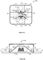
- Figure 2A shows a top view which is taken from a contact side of a module carrier tape segment 20 having a plurality of conductive contact pads, e.g. IC connector having six ISO designated contact pads.
- Figure 2B shows a bottom view which is taken from a bonding side of the module tape segment 20 of Figure 2A having a plurality of holes according to one embodiment of the invention.
- Figure 2C is a see-through view of Figure 2B , wherein the footprints of the contact pads and the encapsulation are in dashed lines.
- the module carrier tape segment 20 comprises a non-conductive substrate 21, e.g. glass epoxy, having a first and a second side.
- a plurality of through holes 22, 23 perforate the substrate 21 wherein each hole extends from the first to the second side of the substrate 21.
- ISO International Organization for Standardization
- the external side of the contact pads make electrical contact with a contact-type smart card reader or electronic terminal to allow signal transmission between the card reader and an IC chip electrically connected to the contact pads.
- the internal side of a contact pad is accessible through one of the holes to allow one or more conductive elements to be disposed therethrough to establish electrical connection with the contact pad.
- FIGS 2B and 2C show two sets of the holes 22, 23 having unequal dimensions, e.g. diameters, and/or different shapes.
- the first set of holes 22 may be hereinafter referred to as “multi-bond holes” or “enlarged holes” which are greater or larger in size, area and/or diameter relative to the second set of holes.
- Each multi-bond hole 22 is configured to receive multiple conductive elements, e.g. wire bond(s), antenna wire/terminals and/or other conductive element.
- Each multi-bond hole 22 may be formed of a plurality of interconnected apertures, e.g. a first aperture 22a and a second aperture 22b fluidly connected to each other.
- the first and the second aperture 22a, 22b may have unequal dimensions, e.g. diameters.
- the interconnection between the first aperture 22a and second aperture 22b may optionally be referred to as a third aperture 22c which is constricted relative to the first and the second aperture 22a, 22b.
- a diameter of the second aperture 22b is greater than a diameter of the first aperture 22a, e.g. by at least two times.
- the first aperture 22a may have a diameter of about 0.6 mm to about 0.9 mm, while the second aperture 22b may have a diameter of about 2.0 mm.
- the first and the second aperture 22a, 22b may taper towards the constricted third opening 22c, but it is to be appreciated that other examples may not include tapering of the first and the second aperture 22a, 22b towards each other.
- a multi-bond hole may be provided as two partially overlapping circular apertures. It is to be appreciated that multi-bond holes may take on other shapes and/or arrangements which may not have been illustrated in the accompanying Figures. For example, a multi-bond hole may be formed of one or more polygons and/or irregular shapes which overlap or interconnect with each other.
- the second set of holes 23 may be hereinafter referred to as "single-bond holes” or “small holes” which are smaller in size, area and/or diameter compared to the first set.
- Each single-bond hole 23 may be configured to receive a single conductive element, e.g. wire bond, and has a diameter of about 0.6 mm to about 0.9 mm.
- each single-bond hole 23 may have same size, area and/or diameter as the first aperture 22a of a multi-bond hole 22.
- multi-bond holes may be provided with mutually distinct shapes and/or dimensions.
- some of the multi-bond holes may have shapes and/or dimensions distinct from single-bond holes, as described above, while a remaining of the multi-bond holes may have shapes and/or dimensions similar to the single-bond holes 23, e.g. diameter of about 0.6 mm to about 0.9 mm, but configured to receive two or more conductive elements, e.g. wire bonds, therein.
- each single-bond hole 23 provides access to a contact pad which has been designated for use based on existing ISO or industry standards as a signal pin-out.
- an IC connector on an IC card or smart card provide six or eight contact pads and at least some of these contact pads are electrically connected to IC chip(s) embedded in the card body.
- the contact pads are designated as C1 to C8, where C1 is designated for supply voltage Vcc, C2 is designated for reset signal RST, C3 is designated for clock signal CLK, C4 is designated for ground GND, C6 is designated for programming input voltage Vpp (optional) and C7 is designated for input/output signal I/O. C4 and C8 are designated as reserved for future use and are commonly unused.
- contact pads C1 to C3 and C5 to C7 may respectively correspond to six contact pads 24a to 24c and 24e to 24g, however, it is to be appreciated that the aforementioned designations and/or arrangement may be adapted according to modifications in ISO or industry standards.
- the conductive pads include a first pair of contact pads, which may be hereinafter referred to as "module-side antenna contact pads" 25a, 25b, and contact pads 24a, 24b, 24c, 24e, 24f, 24g.
- these contact pads are two distinct or mutually exclusive pairs of contact pads, e.g. (24a, 24e) and (24c, 24g).
- the module-side antenna contact pads 25a, 25b are respectively juxtaposed between the two mutually exclusive pairs of contact pads (24a, 24e) and (24c, 24g), i.e. 25a is juxtaposed between 24a and 24e while 25b is juxtaposed between 24c and 24g.
- the contact pads other than the module-side antenna contact pads i.e. six ISO designated contact pads C1, C2, C3, C5, C6 and C7 respectively corresponding to 24a to 24c, 24e to 24g, may be arranged along first opposed edge portions, e.g. opposed width edges, of the substrate 21 at locations which are ISO designated contact locations.
- the module-side antenna contact pads 25a, 25b and the two mutually exclusive pairs of contact pads (24a, 24c) and (24e, 24g) are arranged along second opposed edge portions, e.g. opposed length edges, of the substrate 21.
- the two mutually exclusive pairs of contact pads (24a, 24c) and (24e, 24g) may be arranged at locations which are ISO designated contact locations, however, the module-side antenna contact pads 25a, 25b are located at non-ISO designated contact locations.
- the pair of first opposed edge portions and the pair of second opposed edge portions are generally mutually transverse. If the substrate 21 or module tape segment 20 has a generally rectangular or square shape, the two mutually exclusive pairs of contact pads (24a, 24c) and (24e, 24g) may be, but not necessarily, arranged at corner or near-corner portions of the substrate 21.
- the module-side antenna contact pads 25a, 25b are non-overlapping with ISO designated locations of C1 to C3 and C5 to C7 contact pads on an IC connector, e.g. 24a to 24c, 24e to 24g.
- the module-side antenna contact pads 25a, 25b are arranged at locations on an IC connector, which are undesignated or unspecified by existing ISO or industry standards whether for current use or reserved for future use.
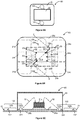
- Figure 3A shows a bottom view which is taken from a bonding side of an IC module 30a according to one embodiment of the invention.
- Figure 3B is a see-through view of Figure 3A , wherein the footprints of the contact pads and the encapsulation are in dashed lines.
- Figure 3C is a cross-sectional view of the IC module 30a taken along line A-A in Figure 3B, and
- Figure 3D is a partial close-up view of Figure 3C .
- the IC module 30a comprises the module carrier tape segment 20 of Figures 3A and 3B , a first IC chip 31a arranged, e.g.
- first conductive elements 32 electrically connecting at least some of the contact pads to the first IC chip 31a, and an encapsulant 33 deposited on the first IC chip 31a and the first conductive elements 32.
- the first conductive elements 32 traverse the holes 22, 23 to electrically connect the internal sides of the contact pads to on-chip pads of the first IC chip 31a, such as by wire-bonding process.
- each hole 23 receives therein a single first conductive element 32; for at least some of the multi-bond holes 22, each hole 22 receives therein multiple conductive elements, including one or more first conductive element 32 electrically connecting module-side antenna contact pad 25a/ 25b to one or more IC chips and a connection to an antenna coil.
- the encapsulant or encapsulation 33 is deposited on the first IC chip 31a and the first conductive elements 32 to encapsulate, e.g. fully enclose, them and protect them from exposure and damage. Particularly, the encapsulant 33 is deposited into single-bond holes 23 having first conductive elements 32 such that these single-bond holes 23 are fully filled and conductive elements therein are encapsulated. The encapsulant 33 is further deposited into a pair of multi-bond holes 22, such that these multi-bond holes 22 are partially filled with encapsulant 33 and partially void of encapsulant.
- a boundary between the first and the adjoining second bonding area 241, 242 is therefore provided by an edge or part thereof of the encapsulant 33 which is disposed on the module-side antenna contact pads 25a / 25b.
- the encapsulant 33 encapsulates a first pair of the first conductive elements 32 which respectively traverse the pair of multi-bond holes 22, and is deposited on or overlays a portion of an internal side of the module-side antenna contact pads 25a, 25b.
- Each portion, being deposited or overlaid with the encapsulant 33, is defined as the first bonding area 241 of a module-side antenna contact pad 25a / 25b, while the encapsulated channel within multi-bond hole 22 is defined as the first bonding channel 221 (see Figure 3D ).
- the encapsulant seals this first bonding area 241 and therefore prevents access to the first bonding area 241, as well as the first bonding channel 221, by other non-encapsulated elements, e.g.
- the first bonding area 241 and the first bonding channel 221 are inaccessible at least for the purpose of receiving electrical connection, e.g. conductive elements.
- the unencapsulated channel within the multi-bond hole 22 is defined as the second bonding channel 222 (see Figure 3D ).
- This second bonding area 242, being devoid of encapsulation, is accordingly accessible or exposed through the second bonding channel 222 within the multi-bond hole 22 to provide a surface for establishing electrical connection to the first IC chip 31a via the respective module-side antenna contact pad 25a / 25b.
- the first bonding area 241 is located at an opposed relation to the first aperture 22a of the multi-bond hole, e.g. the first bonding area 241 is directly under the first aperture 22a.
- the second bonding area 241 is arranged at an opposed relation to the second aperture 22b of the multi-bond hole 22, e.g. the second bonding area 242 is directly under the second aperture 22b.
- This relative arrangement of bonding area and apertures as illustrated in Figures 3C and 3D may vary in other embodiments.
- first and the second bonding area 241, 242 are adjoining and electrically connected to each other, while the first and the second bonding channel 221, 222 are adjoining. It is to be appreciated that the first and the second bonding area 241, 242 are integral portions of one module-side antenna contact pad 25a / 25b and located on a same side thereof. It is to be appreciated that the second bonding area 242 may be at least two times larger than the first bonding area 241.
- the encapsulation 33 which is deposited on module-side antenna contact pads 25a / 25b, partitions each module-side antenna contact pad 25a / 25b as well as the multi-bond hole 22 accessing the same module-side antenna contact pad to provide mutually exclusive channels for accommodating different electrical connections and/or types thereof.
- the first and the second bonding area 241, 242 (or the first and the second bonding channels 221, 222) are partitioned without requiring a presence of substrate therebetween to function as partition, and therefore reduces a footprint or size requirement of the contact pads.
- dimensions, shape and/or arrangement of the contact pads do not need to be substantially altered.
- Figure 3E shows the IC module 30a of Figures 3A to 3D being worked upon to establish electrical connection to an antenna coil 37 which is incorporated or embedded in a card body.
- a method for fabricating a smart card is described as follows with reference to Figures 3E, 3F and 3G wherein Figure 3G shows a smart card 300 incorporating the IC module 30a, and with further reference to the flowchart of Figure 10 .
- the method is equally applicable to IC modules 30b, 30c, 70, 80, 90 of Figures 4A, 4B , 5A, 5B , 7B, 7C , 8B, 8C , 9B, 9C .
- one or more IC modules 30a having encapsulation, are provided.
- an antenna-connecting element e.g. conductive or solder paste 35, is deposited on each second bonding area 242 of the module-side antenna contact pads 25a, 25b (see Figure 3E ).
- the IC module 30a is brought near a card body 36, wherein cavities have been milled in the card body 36 to a depth that is sufficient to expose portions or terminals of the antenna coil 37.
- an exposed terminal 37a of the antenna coil 37 is brought into proximity of or contact with the second bonding area 242.
- the antenna-connecting element is subject to reflow wherein heat is applied to melt the conductive paste 35.
- the melted conductive paste 35 is allowed to cool or cure to form a bond, e.g. rigid conductive bump 35, with the exposed terminal 37a of the antenna coil 37 and with the second bonding area 242 of a module-side antenna contact pad 25a / 25b.
- the IC module 30a which is now electrically connected to the antenna coil 37, may be now be implanted onto a card body 36 to produce a smart card 300.
- an adhesive e.g. glue tape
- the bonding side of the IC module 30a e.g. substrate 21.
- heat may be applied to activate the adhesive, if necessary.
- the bonding side of the IC module 30a may be arranged facing towards or placed in a module cavity formed in the card body 36.
- pressure may be applied such that applied pressure and activated adhesive respectively implants and bonds the IC module 30a to the card body 36 to produce a smart card 300.
- Other steps e.g. hot stamping, may be taken to customise the card body 36 or smart card 300 according to the intended usage.
- the above-described method for fabricating a smart card may be modified by combining the step of establishing electrical connection between antenna coil 37 and module-side antenna contact pads 25a, 25b and the step of implanting an IC module 30a onto a card body 36 into a single step.
- the modified method is described below with reference to the flowchart of Figures 11 and 9D to 9G .
- the method is equally applicable to IC modules 30a, 30b, 30c, 70, 80 of Figures 3B, 3C , 3G , 4A, 4B , 5A, 5B , 7B, 7C , 8B, 8C .
- one or more IC modules 90 having encapsulation, are provided.
- an antenna-connecting element 39a e.g. conductive or solder ribbon or paste, is deposited on a second bonding area 242 of each module-side antenna contact pad 25a / 25b (see Figures 9D and 9E for antenna-connecting element 39a prior to reflow).
- the antenna-connecting element 39a is subject to reflow wherein heat is applied to melt the antenna-connecting element 39a and bond it to the second bonding area 242 of a module side antenna contact pad 25a / 25b (see Figures 9F and 9G for antenna-connecting element 39b after reflow).
- Reflow of the antenna-connecting element also controls or defines the height of the antenna-connecting element.
- Reflow of the antenna-connecting element also at least partially fills the second bonding area with the antenna-connecting element.
- the module-side antenna contact pad 25a / 25b may have a thickness (t1) of about 70 micro meters ( ⁇ m), the substrate and contact pad 25a / 25b may have a combined thickness (t2) of about 190 ⁇ m ⁇ 20 ⁇ m, the module-side antenna contact pad 25a / 25b and antenna-connecting element 39b have a combined thickness (t3) of about 300 micro meters ( ⁇ m) ⁇ 80 ⁇ m, and the module may have a thickness (t4) of up to about 600 ⁇ m.
- an adhesive may be applied to the bonding side of the IC module, e.g. substrate 21.
- the IC module together with the reflowed antenna-connecting element 39b and adhesive applied thereto, is disposed in a module cavity of the card body 36 with the second side of the substrate facing the module cavity of the card body 36 while the antenna-connecting element is disposed in proximity and/or contact with an exposed terminal 37a of the antenna coil 37.
- Heat and pressure are applied to the card body 36 and the IC module 30a disposed therein. The applied heat melts the antenna-connecting element 39b as well as activates the adhesive.
- Each antenna-connecting element 39b further forms a bond with the exposed terminal 37a (or card-side antenna contact pad in certain embodiments) to establish electrical connection between antenna coil 37 and module-side antenna contact pad 25a / 25b through the antenna-connecting element.
- the applied pressure and activated adhesive respectively implants and bonds the IC module 30a to the card body 36 to produce a smart card 300.
- Figure 3G shows a smart card 300 in which the IC module 30a of Figure 3A to 3C has been implanted onto or bonded to a card body 36 using any of the above-described or other methods.
- the card body 36 may have been produced by laminating layers, e.g. plastic substrate, and milling a module cavity in the laminated layers, which is constructed and arranged to accommodate the IC module 30a.
- the laminated layers include a layer incorporating or embedding an antenna coil 37 for implementing contactless interface.
- antenna of the smart card enters a magnetic field produced by the card reader to induce an alternating current which is converted to power the IC chip and allow data transmission between the IC chip in the IC module and the card reader in a contactless manner.
- the IC module 30a is disposed in the module cavity.
- the arrangement of the card body 36, the adhesive 41 as well as the substrate 21, module-side antenna contact pad 25a / 25b and encapsulation 33 of the IC module 30a define a space or enclosure 301.
- This space 301 or enclosure is arranged or aligned under the second aperture 22b of a multi-bond hole 22 such that the second bonding area 242 of the module-side antenna contact pad is accessible or exposed through the space 301, the second aperture 22b and the second bonding channel 222.
- An antenna-connecting element e.g.
- the antenna-connecting element establishes an electrical connection between the antenna coil 37 embedded in the card body 36 and the module-side antenna contact pad 25a / 25b.
- the first aperture 22a is at least substantially filled with encapsulant 33 in order to seal the first bonding area while the second aperture is unfilled or at most partially filled with encapsulant 33 in order to accommodate an antenna-connecting element 39, e.g. conductive bump 35, and exposed terminals 37a of antenna coil 37.
- the constricted third aperture 22c interconnecting the first and the second aperture 22a, 22b may be filled or unfilled.
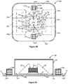
- Figure 4A shows a see-through view which is taken from a bonding side of an IC module 30b according to another embodiment of the invention, wherein the footprints of the contact pads and the encapsulation are in dashed lines.
- Figure 4B is a cross-sectional view of the IC module 30b taken along line B-B in Figure 4A . As illustrated, for at least some of the single-bond holes 23, each hole 23 receives therein a single first conductive element 32; for the multi-bond holes 22, each hole 22 receives therein multiple conductive elements, including a first and a second pair of first conductive elements 32.
- first and the second pair of first conductive elements 32 electrically connect a module-side antenna contact pad 25a / 25b to different on-chip pads of the first IC chip 31a.
- These first and second pair of first conductive elements 32 traverse the first aperture 22a of the multi-bond hole 22 and are encapsulated by an encapsulant 33.
- the encapsulant 33 is deposited on a portion of the module-side antenna contact pad to define a first bonding area 241.
- the encapsulation seals the first bonding area 241 and prevents access thereto.
- the encapsulation also defines a first bonding channel 221 terminating at the first bonding area 241.
- a second bonding area 242 on the module-side antenna contact pad 25a / 25b, being adjoining and electrically connected to the first bonding area 241, is not deposited with the encapsulant 33 and therefore remains accessible or exposed through a second bonding channel 222 terminating at the second bonding area 242, e.g. through the second aperture 22b of the multi-bond hole 22.
- This second bonding area 242, being devoid of encapsulation, is accordingly accessible or exposed through the multi-bond hole 22 as a surface for establishing electrical connection to the first IC chip 31a.
- Figure 4C shows the IC module 30b of Figures 4A to 4B being worked upon to establish electrical connection to an antenna coil 37 which is incorporated in a card body.
- Other features and characteristics of the IC module 30b, method of establishing electrical connection with antenna coil 37 and method of implanting the IC module 30b, as illustrated by Figures 4A to 4D would be similar to the foregoing description in relation to Figures 3A to 3G , 10 and 11 , and therefore their details will not be reproduced here.
- a smart card implanted with the IC module 30b of Figures 4A to 4B would be similar to the foregoing description in relation to Figures 3A to 3G , and therefore its details will not be reproduced here.
- Figure 5A shows a see-through view which is taken from a bonding side of an IC module 30c according to yet another embodiment of the invention, wherein the footprints of the contact pads and the encapsulation are in dashed lines.
- Figure 5B is a cross-sectional view of the IC module taken along line C-C in Figure 5A .
- the IC module 30c comprises a first IC chip 31a and a second IC chip 31b arranged on the second side of the substrate 21.
- a plurality of first conductive elements 32 traverse at least some of the single-bond holes 23 and multi-bond holes 22, and electrically connect at least some of the contact pads, including module-side antenna contact pads 25a, 25b, to on-chip pads of the first IC chip 31a.
- a plurality of second conductive elements 42 respectively traverse the pair of multi-bond holes and, electrically connect the module-side antenna contact pads 25a, 25b to the second IC chip 31b. Second conductive elements 42 may further electrically connect the second IC chip 31 b to other contact pads (not shown).
- Those first and second conductive elements 32, 42, which traverse the first aperture 22a of the multi-bond holes, are encapsulated by an encapsulant 33. Similar to the embodiment of Figures 3A to 3G , the encapsulant 33 is deposited on a portion of the contact pad 25a / 25b to define a first bonding area 241. The encapsulation seals the first bonding area 241 and prevents access thereto.
- the encapsulation also defines a first bonding channel 221 terminating at the first bonding area 241.
- a second bonding area 242 on the module-side antenna contact pad 25a / 25b, being adjoining and electrically connected to the first bonding area 241, is not deposited with the encapsulant 33 and therefore remains accessible through a second bonding channel 222 terminating at the second bonding area 242, e.g. through the second aperture 22b of the multi-bond hole 22.
- This second bonding area 241, being devoid of encapsulation, is accordingly accessible or exposed through the multi-bond hole 22 as a surface for establishing electrical connection to the appropriate one of the first and the second IC chip 31a, 31b.
- Figure 5C shows the IC module 30c of Figures 5A to 5B being worked upon to establish electrical connection to an antenna coil 37 which is incorporated in a card body.
- Other features and characteristics of the IC module 30c, method of establishing electrical connection with antenna coil 37 and method of implanting the IC module 30c, as illustrated by Figures 5A to 5D would be similar to the foregoing description in relation to Figure 3A to 3G , 10 and 11 , and therefore their details will not be reproduced here.
- a smart card implanted with the IC module 30c of Figures 5A to 5B would be similar to the foregoing description in relation to Figures 3A to 3G , and therefore its details will not be reproduced here.
- Figure 6A shows a top view which is taken from a contact side of a module carrier tape segment 60 having a plurality of conductive contact pads, e.g. IC connector having eight ISO designated contact pads.
- Figure 6B shows a bottom view which is taken from a bonding side of the module tape segment 60 of Figure 6A having a plurality of holes according to one embodiment of the invention.
- Figure 6C is a see-through view of Figure 6B , wherein the footprints of the contact pads and the encapsulation are in dashed lines.
- the conductive pads include a first pair of contact pads, which may be hereinafter referred to as "module-side antenna contact pads" 25a, 25b, and contact pads 24a, 24b, 24c, 24d, 24e, 24f, 24g, 24h.
- these contact pads are at least two distinct or mutually exclusive pairs of contact pads, e.g. (24a, 24e) and (24d, 24h).
- the module-side antenna contact pads 25a, 25b are respectively juxtaposed between the two mutually exclusive pairs of contact pads, i.e. 25a is juxtaposed between 24a and 24e while 25b is juxtaposed between 24d and 24h.
- Module-side antenna contact pad 25b may be further juxtaposed between 24c and 24g.
- the contact pads other than the module-side antenna contact pads may be arranged along first opposed edge portions, e.g. opposed width edges, of the substrate 21 at locations which are ISO designated contact locations.
- the module-side antenna contact pads 25a, 25b and the two mutually exclusive pairs of contact pads (24a, 24e) and (24d, 24h) are arranged along second opposed edge portions, e.g. opposed length edges, of the substrate 21.
- the two mutually exclusive pairs of contact pads (24a, 24e) and (24d, 24h) may be arranged at locations which are ISO-designated contact locations, however, the module-side antenna contact pads 25a, 25b are located at non-ISO designated contact locations.
- the pair of first opposed edge portions and the pair of second opposed edge portions are generally mutually transverse. If the substrate 21 has a generally rectangular or square shape, the two mutually exclusive pairs of contact pads (24a, 24e) and (24d, 24h) may be, but not necessarily, arranged at corner or near-corner portions of the substrate 21 and non-overlapping with C4 and C8 contact pads.
- the module-side antenna contact pads 25a, 25b are non-overlapping with ISO designated locations of C1 to C8 contact pads on an IC connector, e.g. 24a to 24h.
- the module-side antenna contact pads 25a, 25b are arranged at locations on an IC connector, which are undesignated or unspecified by existing ISO or industry standards whether for current use or reserved for future use.
- the module-side antenna contact pads 25a, 25b are non-overlapping with contact pads designated by ISO 7816 as reserved for future use, e.g. C4 and C8 contact pads.
- Figure 7A shows a bottom view which is taken from a bonding side of an IC module 70 according to one embodiment of the invention.
- Figure 7B is a see-through view of Figure 7A , wherein the footprints of the contact pads and the encapsulation are in dashed lines.
- Figure 7C is a cross-sectional view of the IC module 70 taken along line D-D in Figure 7B .
- an IC module 70 of Figure 7A to 7C may be modified to provide other embodiments.
- an IC module 70 may have multiple first conductive elements 32 traversing the multi-bond holes 25a, 25b, which is similar to the foregoing description in relation to Figures 4A to 4D , and therefore its details will not be reproduced here.
- an IC module 70 may have multiple IC chips being separately connected to the module-side antenna contact pads 25a, 25b, which is similar to the foregoing description related to Figures 5A to 5D and therefore its details will not be reproduced here.
- the first and the second aperture 22a, 22b may have different shapes and/or unequal dimensions, e.g. width, length.
- the first and the second aperture are located at an opposed relation to the first and the second bonding area respectively, wherein the first aperture includes a width which is constricted relative to a width/diameter of the second aperture.
- Such configuration of multi-bond holes may be varied as follows.
- the first aperture of at least one of the first pair of multi-bond holes includes a length which is greater than or equal to a distance between two of the single-bond holes which are formed in adjacent or non-adjacent ones of the contact pads. In one embodiment, the first aperture of at least one of the first pair of multi-bond holes is arranged between the first IC chip (or an area on the second side of the substrate which is adapted for arranging the first IC chip) and at least one single-bond hole.
- the first aperture of the at least one of the first pair of multi-bond holes is at least partially arranged in conformity with a contour defined by at least one of the sides of the first IC chip (or of the area on the second side of the substrate which is adapted for arranging the first IC chip).
- a third aperture, fluidly connecting between the first and the second aperture includes a width which is constricted relative to the width of the first aperture and the width of the second aperture.
- Figure 8A shows a bottom view which is taken from a bonding side of an IC module 80 according to one embodiment of the invention.
- Figure 8B is a see-through view of Figure 8A , wherein the footprints of the contact pads and the encapsulation are in dashed lines.
- Figure 8C is a cross-sectional view of the IC module 80 taken along zig-zag line E-E in Figure 8B .
- Figure 9A shows a bottom view which is taken from a bonding side of an IC module 90 according to one embodiment of the invention.
- Figure 9B is a see-through view of Figure 9A , wherein the footprints of the contact pads and the encapsulation are in dashed lines.
- Figure 9C is a cross-sectional view of the IC module 90 taken along line F-F in Figure 9B .
- features and characteristics of the IC module 80, 90, method of establishing electrical connection with antenna coil 37 and method of implanting the IC module 80, 90 would be similar to the foregoing description in relation to Figures 3A to 3G , 10 and 11 , and therefore their details will not be reproduced here.
- a smart card implanted with the IC module 80, 90 would be similar to the foregoing description in relation to Figures 3A to 3G , and therefore its details will not be reproduced here.
- each multi-bond hole 122 may be formed of a plurality of interconnected apertures, e.g. a first aperture 122a and a second aperture 122b fluidly connected to each other.
- a diameter/width of the second aperture 122b may be greater than a diameter/width of the first aperture 122a, e.g. by at least two times.
- the interconnection between the first aperture 122a and the second aperture 122b may optionally be referred to as a third aperture 122c.
- the third aperture 122c may be constricted relative to the second aperture 122b (see Figures 8A to 8C , 9A to 9C ) or to both the first and the second aperture 122a, 122b (not shown).
- the first aperture 122a is generally elongated, e.g. its length is greater in relation to its width. At least part of the first aperture 122a is arranged or interposed between the first IC chip 31a and at least one single-bond hole 23.
- the first aperture 122a, or part thereof, may have an aperture length which traverses the substrate 21 at least partially along a side of the first IC chip 31a.
- the first IC chip 31a has a plurality of sides which may be generally non-parallel, e.g. orthogonal, to the substrate 21.
- the aperture length traversing at least partially along a side of the first IC chip 31a may be greater than or equal to a distance between two adjacent single-bond holes formed in adjacent contact pads. This aperture length and this distance between two adjacent single-bond holes 23 may be taken along a surface of the substrate 21 on which the single-bond holes 23 and multi-bond holes 22 are arranged or formed.
- the first aperture 122, or part thereof is at least partially arranged in conformity with a contour defined by one or more sides of the first IC chip.
- the first aperture 122a, or part thereof is parallel to one side of the first IC chip 31a.
- the first aperture 122a is provided as mutually-orthogonal aperture paths or sections, e.g. L-shape, and is parallel to two adjoining sides, e.g. orthogonal sides, of the first IC chip 31a.
- each first aperture 122a or part thereof defines one or more straight/linear paths or sections, it is to be appreciated that each first aperture 122a or part thereof may define a curve/non-linear path or section.
- Each second aperture 122b may be circular or formed of polygon and/or irregular shape.
- Each third aperture 122c if any, may define a straight/linear or curve/non-linear path.
- an antenna-connecting element i.e. an electrical connection between the module-side antenna contact pad 25a / 25b and antenna coil 37 embedded in the card body, is provided by a conductive bump 35.
- the antenna-connecting element may be provided by other conductive means in other embodiments.
- Such antenna-connecting element may be a conductive disc which is an elastomeric material comprising conductive particles, or a flexible conductive bump which may be dispensed as an electrically conductive adhesive, e.g. in paste form, and curable into a rigid form.
- the conductive disc or flexible conductive bump may be deposited on the card-side antenna contact pad before curing and/or before implanting the IC module onto the card body.
- the exposed terminals 37a are extracted portions of an embedded antenna coil 37. It is to be appreciated that in other embodiments, instead of extracting terminals 37a of the antenna coil 37 from the card body, a card-side antenna contact pad (not shown) may be arranged in the module cavity of the card body and is electrically connected to the embedded antenna coil 37. An antenna-connecting element may be interposed and/or abutted between the module-side antenna contact pad and the card-side antenna pad to establish an electrical connection therebetween.
- a method for fabricating an integrated module for a dual interface smart card is described as follows.
- a workpiece comprising a non-conductive substrate having a plurality of single-bond holes and a pair of multi-bond holes, both extending through a first and a second side of the substrate, a plurality of conductive contact pads, including a first pair thereof, arranged over the holes and on the first side of the substrate, a first and/or second IC chips arranged on the second side of the substrate, and a plurality of first and/or second conductive elements traversing the holes and electrically connecting the contact pads to the first and/or second IC chips.
- a first pair of first conductive elements respectively traverse the pair of multi-bond holes and electrically connect the first pair of contact pads to the first IC chip.
- the workpiece is subject to an encapsulation process to encapsulate the IC chip(s) and conductive element(s), and to define a first and a second bonding area on the module-side antenna contact pad as well as a first and a second bonding channel.
- the encapsulant is deposited over the IC chip(s) and the conductive elements in the single-bond holes, and fills the single-bond holes.
- the encapsulant is also deposited into a multi-bond hole such that a first aperture of the multi-bond hole is filled with encapsulation which defines a first bonding channel and seals the first bonding area, while conductive element(s) in the first bonding channel are encapsulated.
- Any constricted third aperture connected to the first aperture may also be filled or partially filled as appropriate.
- the second aperture of a multi-bond hole is unfilled or at most partially filled with encapsulation such that a second bonding channel provides access to a second bonding area on the module-side antenna contact pad to allow electrical connection thereto.
- the partitioning of the first and the second bonding area and channel is performed by deposition of encapsulation on the module side antenna contact pad 25a /25b and without arranging or interposing a substrate between the first and the second bonding area and channel.
- the extent of the first and the second bonding area on the module-side antenna contact pad may be determined by the encapsulation process.
- the dam material defines a perimeter of the first bonding area such that the remaining area on the module-side antenna contact pad, which is outside the dam perimeter, is defined as the second bonding area.
- the dam material may be deposited into the first aperture 22a / 122a or constricted third aperture 22c / 122c of a multi-bond hole 22 and the encapsulant is dispensed into the first aperture to define a first bonding area which is sized approximate to the first aperture.
- the dam material may be deposited into the second aperture 22b / 122b of a multi-bond hole 22 and the encapsulant is dispensed into the first aperture 22a / 122a to define a first bonding area which is larger than the first aperture.
- the dam material may determine a perimeter of the encapsulation region prior to dispensing an encapsulant within the perimeter of the dam material, to thereby apportion or partition a first and a second bonding area within the multi-bond hole.
- the invention is therefore distinct over WO 2015/173514 A1 (hereinafter ''514 publication).
- the edge of its encapsulation area terminates at the electrically insulating substrate in accordance with common industry practice.
- Figure 4 of the ''514 publication shows that a circle corresponding to the encapsulation area of the chip and its connection wires leaves the oblong holes free so that they can subsequently be connected to an antenna.
- Figures 5 to 7 then show various ways in which a conductive land is connected to an antenna through the oblong hole.
- FIG. 5 shows two wire connections established in the oblong hole which is devoid of encapsulation-however, this example may result in crossing of the two wires, which would lead to electrical shorting and/or breakage of the two wires.
- a portion of insulating substrate is used to create two separate holes (a round connection well and an oblong blind hole)-however, these examples may experience increased difficulty in applying adhesion to bonding side of the chip card module and reduce adhesion area on the bonding side / adhesion capability thereof.
- the ICC or smart cards according to the invention may be used in various applications, including but not limited to, commercial or financial applications, e.g. banking, credit/debit card, stored value, electronic cash, loyalty system, identification, ticketing, parking and toll collection; mobile telecommunications; and information technology, e.g. access control, secured authentication.
- commercial or financial applications e.g. banking, credit/debit card, stored value, electronic cash, loyalty system, identification, ticketing, parking and toll collection
- mobile telecommunications e.g. access control, secured authentication.
Landscapes
- Engineering & Computer Science (AREA)
- Microelectronics & Electronic Packaging (AREA)
- Computer Hardware Design (AREA)
- Physics & Mathematics (AREA)
- General Physics & Mathematics (AREA)
- Theoretical Computer Science (AREA)
- Computer Networks & Wireless Communication (AREA)
- Credit Cards Or The Like (AREA)
- Variable-Direction Aerials And Aerial Arrays (AREA)
- Geometry (AREA)
- Combinations Of Printed Boards (AREA)
- Pinball Game Machines (AREA)
Claims (32)
- Integriertes Schaltungs-(IS)-modul (30a, 30b, 30c, 70, 80, 90) für eine Chipkarte sowohl mit Kontaktschnittstelle als auch mit kontaktloser Schnittstelle, das IS-Modul Folgendes umfassend:ein nichtleitendes Substrat (21) mit mehreren Einzelverbindungslöchern (23) und einem Paar Mehrfachverbindungslöchern (22), die sich beide von einer ersten zu einer zweiten Seite des Substrats (21) erstrecken, wobei jedes Mehrfachverbindungsloch (22) größer ist als jedes Einzelverbindungsloch (23) und eingerichtet ist, um mehrere leitfähige Elemente aufzunehmen, wobei jedes Einzelverbindungsloch (23) eingerichtet ist, um ein einzelnes leitfähiges Element aufzunehmen;mehrere leitfähige Kontaktflächen (24a, 24b, 24c, 24e, 24f, 24g, 25a, 25b), die ein erstes Paar davon (25a, 25b) umfassen, das auf der ersten Seite des Substrats (21) angeordnet ist;einen ersten IS-Chip (31a), der auf der zweiten Seite des Substrats (21) angeordnet ist;mehrere erste leitfähige Elemente (32), die durch die Einzelverbindungslöcher und das Paar Mehrfachverbindungslöcher (23, 22) laufen und die mindestens einige der Kontaktflächen (24a, 24b, 24c, 24e, 24f, 24g, 25a, 25b) mit dem ersten IS-Chip (31a) elektrisch verbinden, wobei die ersten leitfähigen Elemente (32) ein erstes Paar erster leitfähiger Elemente (32) umfassen, die jeweils durch das Paar Mehrfachverbindungslöcher (22) laufen und die das erste Paar Kontaktflächen (25a, 25b) mit dem ersten IS-Chip (31a) elektrisch verbinden; undgekennzeichnet durcheine Einkapselung (33), die auf dem ersten IS-Chip (31a), auf den ersten leitfähigen Elementen (32) und auf dem ersten Paar Kontaktflächen (25a, 25b) abgeschieden wurde, wobei ein Rand der Einkapselung (33), die auf dem ersten Paar Kontaktflächen (25a, 25b) abgeschieden wurde, jedes des Paares Mehrfachverbindungslöcher (22) in einen verkapselten ersten Verbindungskanal (221) und in einen angrenzenden nicht verkapselten zweiten Verbindungskanal (222) zuteilt, die jeweils an einem ersten und an einem angrenzenden zweiten Verbindungsbereich (241, 242) auf jeder des ersten Paares Kontaktflächen (25a, 25b) derartig enden, dass das erste Paar erster leitfähiger Elemente (32) jeweils den ersten Verbindungskanal (221) des Paares Mehrfachverbindungslöcher (22) durchläuft, und weiterhin derartig enden, dass die Einkapselung (33) den ersten Verbindungsbereich (241) abdichtet und den zweiten Verbindungsbereich (242) durch den zweiten Verbindungskanal (222) exponiert, um eine Oberfläche zum Einrichten einer elektrischen Verbindung mit dem ersten IS-Chip (31a) bereitzustellen, wobei die Einkapselung (33) den ersten und den zweiten Verbindungsbereich (241, 242) voneinander unterteilt, ohne ein Vorhandensein des Substrats (21) dazwischen zu erfordern.
- IS-Modul (30a, 30b, 30c, 70, 80, 90) nach Anspruch 1, wobei die ersten leitfähigen Elemente (32) ein zweites Paar erster leitfähiger Elemente (32) umfassen und wobei die Einkapselung (33) weiterhin auf dem zweiten Paar erster leitfähiger Elemente (32) abgeschieden wurde, die jeweils den ersten Verbindungskanal (221) des Paares Mehrfachverbindungslöcher (22) durchlaufen und das erste Paar Kontaktflächen (25a, 25b) mit dem ersten IS-Chip (31a) elektrisch verbinden.
- IS-Modul (30a, 30b, 30c, 70, 80, 90) nach Anspruch 1, weiterhin Folgendes umfassend:einen zweiten IS-Chip (31b), der auf der zweiten Seite des Substrats (21) angeordnet ist; undein Paar zweiter leitfähiger Elemente (42), die jeweils den ersten Verbindungskanal (221) des Paares Mehrfachverbindungslöcher (22) durchlaufen und das erste Paar der Kontaktflächen (25a, 25b) mit dem zweiten IS-Chip (31b) elektrisch verbinden, wobei die Einkapselung (33) weiterhin auf dem Paar zweiter leitfähiger Elemente abgeschieden wurde.
- IS-Modul (30a, 30b, 30c, 70, 80, 90) nach einem der Ansprüche 1 bis 3, wobei der zweite Verbindungsbereich (242) mindestens zweimal größer ist als der erste Verbindungsbereich (241).
- IS-Modul (30a, 30b, 30c, 70, 80, 90) nach einem der Ansprüche 1 bis 4, wobei die Kontaktflächen zwei sich gegenseitig ausschließende Paare Kontaktflächen umfassen, die andere sind als das erste Paar Kontaktflächen (25a, 25b), und wobei das erste Paar Kontaktflächen (25a, 25b) jeweils zwischen den beiden sich gegenseitig ausschließenden Paaren Kontaktflächen nebeneinanderliegend sind.
- IS-Modul (30a, 30b, 30c, 70, 80, 90) nach Anspruch 5, wobei die anderen Kontaktflächen als das erste Paar Kontaktflächen (25a, 25b) entlang ersten gegenüberliegenden Randabschnitten des Substrats (21) angeordnet ist, wobei das erste Paar Kontaktflächen (25a, 25b) und die zwei sich gegenseitig ausschließenden Paare Kontaktflächen entlang zweiten gegenüberliegenden Randabschnitten des Substrats (21) angeordnet sind, wobei die ersten und die zweiten gegenüberliegenden Randabschnitte transversal zueinander sind.
- IS-Modul (30a, 30b, 30c, 70, 80, 90) nach einem der Ansprüche 1 bis 4, wobei das erste Paar Kontaktflächen (25a, 25b) nicht überlappend zu den anderen Kontaktflächen als dem ersten Paar Kontaktflächen (25a, 25b) ist.
- IS-Modul (30a, 30b, 30c, 70, 80, 90) nach Anspruch 7, wobei das erste Paar Kontaktflächen (25a, 25b) nicht überlappend zu den Kontaktflächen ist, die durch ISO 7816 als zur zukünftigen Verwendung reserviert festgelegt sind.
- IS-Modul (30a, 30b, 30c, 70, 80, 90) nach einem der Ansprüche 1 bis 8, wobei jedes des Paares Mehrfachverbindungslöcher (22) aus mindestens einer ersten und einer zweiten Öffnung (22a, 22b) ausgebildet ist, die flüssig miteinander verbunden sind und in einer gegenüberliegenden Beziehung an dem ersten bzw. an dem zweiten Verbindungsbereich (241, 242) angeordnet sind, wobei die erste Öffnung (22a) eine Breite umfasst, die in Bezug auf eine Breite der zweiten Öffnung (22b) verengt ist.
- IS-Modul (30a, 30b, 30c, 70, 80, 90) nach Anspruch 9, wobei die erste Öffnung (22a) von mindestens einem des Paares Mehrfachverbindungslöcher (22) eine Länge umfasst, die größer oder gleich einer Entfernung zwischen zwei der Einzelverbindungslöcher (23) ist, die in benachbarten der Kontaktflächen ausgebildet sind.
- IS-Modul (30a, 30b, 30c, 70, 80, 90) nach einem der Ansprüche 9 bis 10, wobei die erste Öffnung (22a) des mindestens einen des Paares Mehrfachverbindungslöcher zwischen dem ersten IS-Chip (31a) und mindestens einem Einzelverbindungsloch (23) angeordnet ist.
- IS-Modul (30a, 30b, 30c, 70, 80, 90) nach einem der Ansprüche 9 bis 11, wobei der erste IS-Chip (31a) mehrere Seiten umfasst, wobei die erste Öffnung (22a) des mindestens einen Paares Mehrfachverbindungslöcher (22) mindestens teilweise in Übereinstimmung mit einer Kontur angeordnet ist, die durch mindestens eine der Seiten des ersten IS-Chips (31a) definiert ist.
- IS-Modul (30a, 30b, 30c, 70, 80, 90) nach einem der Ansprüche 9 bis 12, wobei eine dritte Öffnung (22c), die zwischen der ersten und der zweiten Öffnung (22a, 22b) flüssig verbunden ist, eine Breite umfasst, die in Bezug auf die Breite der ersten Öffnung (22a) und die Breite der zweiten Öffnung (22b) verengt ist.
- IS-Modul (30a, 30b, 30c, 70, 80, 90) nach einem der Ansprüche 1 bis 8, wobei jedes Paar Mehrfachverbindungslöcher (22) aus zwei sich teilweise überlappenden kreisförmigen Öffnungen ausgebildet ist.
- Chipkarte sowohl mit Kontaktschnittstelle als auch mit kontaktloser Schnittstelle, die Chipkarte Folgendes umfassend:einen Kartenkörper (36) mit einem Modulhohlraum und einer Antennenspule (37);ein Paar Antennenverbindungselemente (35, 39a, 39b);das integrierte Schaltungs-(IS)-modul (30a, 30b, 30c, 70, 80, 90) nach einem der Ansprüche 1 bis 14, das in dem Hohlraum angeordnet ist,gekennzeichnet dadurch, dassan dem zweiten Verbindungskanal (222) eines des Paares der Antennenverbindungselemente (35, 39a, 39b) den zweiten Verbindungskanal (222) durchläuft und zwischen der Antennenspule (37) und dem zweiten Verbindungsbereich (242) derartig verbindet, dass eine elektrische Verbindung zwischen der Antennenspule (37) und dem ersten IS-Chip (31a) hergestellt wird.
- Chipkarte nach Anspruch 15, wobei das Antennenverbindungelement (35, 39a, 39b) einen starren leitfähigen Kontakthöcker oder Lötmittelkontakthöcker (35), eine leitfähige Scheibe oder einen flexiblen leitfähigen Kontakthöcker aufweist, der einen elektrisch leitfähigen Klebstoff umfasst.
- Verfahren zu Herstellung eines integrierten Schaltungs-(IS)-moduls (30a, 30b, 30c, 70, 80, 90) für eine Chipkarte sowohl mit Kontaktschnittstelle als auch mit kontaktloser Schnittstelle, das Verfahren Folgendes umfassend:Bereitstelleneines nichtleitenden Substrats (21) mit mehreren Einzelverbindungslöchern (23) und einem Paar Mehrfachverbindungslöchern (22), die sich beide von einer ersten zu einer zweiten Seite des Substrats (21) erstrecken, wobei jedes Mehrfachverbindungsloch (22) größer ist als jedes Einzelverbindungsloch (23) und eingerichtet ist, um mehrere leitfähige Elemente aufzunehmen, wobei jedes Einzelverbindungsloch (23) eingerichtet ist, um ein einzelnes leitfähiges Element aufzunehmen;mehrerer leitfähiger Kontaktflächen (24a, 24b, 24c, 24e, 24f, 24g, 25a, 25b), die ein erstes Paar davon (25a, 25b) umfassen, das auf der ersten Seite des Substrats (21) angeordnet ist,eines ersten IS-Chips (31a), der auf der zweiten Seite des Substrats (21) angeordnet ist, undmehrerer erster leitfähiger Elemente (32), die durch die Einzelverbindungslöcher (23) und das Paar Mehrfachverbindungslöcher (22) laufen und mindestens einige der Kontaktflächen (24a, 24b, 24c, 24e, 24f, 24g, 25a, 25b) mit dem ersten IS-Chip (31a) elektrisch verbinden, wobei die ersten leitfähigen Elemente (32) ein erstes Paar erster leitfähiger Elemente (32) umfassen, die jeweils durch das Paar Mehrfachverbindungslöcher (22) laufen und das erste Paar Kontaktflächen (25a, 25b) mit dem ersten IS-Chip (31a) elektrisch verbinden; und gekennzeichnet durchAbscheiden einer Einkapselung (33) auf dem ersten IS-Chip (31a), den ersten leitfähigen Elementen (32) und dem ersten Paar Kontaktflächen (25a, 25b), umfassendZuteilen, durch einen Rand der Einkapselung (33), jedes des Paares Mehrfachverbindungslöcher (22) in einen verkapselten ersten Verbindungskanal (221) und in einen angrenzenden nicht verkapselten zweiten Verbindungskanal (222), die jeweils an einem ersten und einem angrenzenden zweiten Verbindungsbereich (241, 242) auf jeder des ersten Paares Kontaktflächen (25a, 25b) enden, wobei das erste Paar erster leitfähiger Elemente (32) jeweils den ersten Verbindungskanal (221) des Paares Mehrfachverbindungslöcher (22) durchläuft,ohne das Substrat (21) zwischen dem ersten und dem zweiten Verbindungsbereich (241, 242) zu erfordern, Unterteilen des ersten Verbindungsbereichs (241) von dem zweiten Verbindungsbereich (242) durch Abdichten des ersten Verbindungsbereichs (241) mit der Einkapselung (33), um den ersten Verbindungskanal (221) zu definieren und den zweiten Verbindungsbereich (242) durch den zweiten Verbindungskanal (222) zu exponieren, um eine Oberfläche zum Einrichten einer elektrischen Verbindung mit dem ersten IS-Chip (31a) bereitzustellen, wodurch das IS-Modul (30a, 30b, 30c, 70, 80, 90) bereitgestellt wird.
- Verfahren nach Anspruch 17, wobei Abscheiden der Einkapselung (33) auf dem ersten IS-Chip (31a), den ersten leitfähigen Elementen (32) und dem ersten Paar Kontaktflächen (25a, 25b) weiterhin Abscheiden der Einkapselung (33) auf einem zweiten Paar erster leitfähiger Elemente (32) umfasst, die jeweils den ersten Verbindungskanal (221) des Paares Mehrfachverbindungslöcher (22) durchlaufen und das erste Paar Kontaktflächen (25a, 25b) mit dem ersten IS-Chip (31a) elektrisch verbinden.
- Verfahren nach Anspruch 17, wobei das Substrat (21) einen zweiten IS-Chip (31b) umfasst, der auf der zweiten Seite des Substrats (21) angeordnet ist, und wobei Abscheiden der Einkapselung (33) auf dem ersten IS-Chip (31a), den ersten leitfähigen Elementen (32) und dem ersten Paar Kontaktflächen (25a, 25b) weiterhin Abscheiden der Einkapselung (33) auf dem zweiten IS-Chip (31b) und einem Paar erster leitfähiger Elemente (42) umfasst, die jeweils den ersten Verbindungskanal (221) des Paares Mehrfachverbindungslöcher (22) durchlaufen und das erste Paar Kontaktflächen (25a, 25b) mit dem zweiten IS-Chip (31b) elektrisch verbinden.
- Verfahren nach einem der Ansprüche 17 bis 19, wobei jedes des Paares Mehrfachverbindungslöcher (22) aus einer ersten und einer zweiten Öffnung (22a, 22b) ausgebildet ist, die durch eine dritte Öffnung (22c) dazwischen flüssig verbunden sind, wobei Abscheiden der Einkapselung (33) auf dem ersten IS-Chip (31a), den ersten leitfähigen Elementen (32) und dem ersten Paar Kontaktflächen (25a, 25b) weiterhin Abgeben der Einkapselung (33) durch die erste Öffnung (22a) und Ermöglichen umfasst, dass die dritte Öffnung (22c), die in Bezug auf mindestens die zweite Öffnung (22b) verengt ist, verhindert, dass die Einkapselung (33) in die zweite Öffnung (22b) fließt.
- Verfahren nach einem der Ansprüche 17 bis 19, wobei vor Abscheiden der Einkapselung (33) auf dem ersten IS-Chip (31a), den ersten leitfähigen Elementen (32) und dem ersten Paar Kontaktflächen (25a, 25b), das Verfahren weiterhin Folgendes umfasst:Abscheiden eines Dammmaterials auf jeder des ersten Paares Kontaktflächen (25a, 25b), um einen Umfang des ersten Verbindungsbereichs (241) zu definieren, undwobei Abscheiden der Einkapselung (33) auf dem ersten IS-Chip (31a), den ersten leitfähigen Elementen (32) und dem ersten Paar Kontaktflächen (25a, 25b) weiterhin Abscheiden der Einkapselung (33) innerhalb des Umfangs umfasst, um den ersten Verbindungsbereich (241) abzudichten.
- Einseitig beschichtetes integriertes Schaltungs-(IS)-Trägerband, das zur Verwendung in einer Chipkarte sowohl mit Kontaktschnittstelle als auch mit kontaktloser Schnittstelle eingerichtet ist, das IS-Trägerband Folgendes umfassend:ein nichtleitendes Substrat (21) mit mehreren Einzelverbindungslöchern (23) und einem Paar Mehrfachverbindungslöchern (22), die sich beide von einer ersten zu einer zweiten Seite des Substrats (21) erstrecken, wobei jedes Mehrfachverbindungsloch (22) größer ist als jedes Einzelverbindungsloch (23) und eingerichtet ist, um mehrere leitfähige Elemente aufzunehmen, wobei jedes Einzelverbindungsloch (23) eingerichtet ist, um ein einzelnes leitfähiges Element aufzunehmen;mehrere leitfähige Kontaktflächen (24a, 24b, 24c, 24e, 24f, 24g, 25a, 25b), die ein erstes Paar davon (25a, 25b) umfassen, das auf der ersten Seite des Substrats (21) angeordnet ist;wobei die zweite Seite des Substrats (21) eingerichtet ist, um mit einem ersten IS-Chip (31a) darauf angeordnet zu sein;wobei mindestens einige der Kontaktflächen (24a, 24b, 24c, 24e, 24f, 24g, 25a, 25b) eingerichtet sind, um mit dem ersten IS-Chip (31a) durch mehrere erste leitfähige Elemente (32) elektrisch zu verbinden, welche die Einzelverbindungslöcher (23) und das Paar Mehrfachverbindungslöcher (22) durchlaufen, wobei das erste Paar Kontaktflächen (25a, 25b) eingerichtet ist, um durch ein erstes Paar der ersten leitfähigen Elemente (32), die das Paar Mehrfachverbindungslöcher (22) durchlaufen, mit dem ersten IS-Chip (31a) elektrisch zu verbinden; unddadurch gekennzeichnet, dassjedes Mehrfachverbindungsloch (22) eingerichtet ist, um durch einen Rand einer Einkapselung (33), die auf dem ersten Paar Kontaktflächen (25a, 25b) abgeschieden werden soll, in einen verkapselten ersten Verbindungskanal (221) und in einen angrenzenden nicht verkapselten zweiten Verbindungskanal (222) zugeteilt zu werden, die jeweils an einem ersten und an einem angrenzenden zweiten Verbindungsbereich (242) auf jeder des ersten Paares der Kontaktflächen (25a, 25b) derartig enden, dass das erste Paar erster leitfähiger Elemente (32) eingerichtet ist, um jeweils den ersten Verbindungskanal (221) des Paares Mehrfachverbindungslöcher (22) zu durchlaufen, und weiterhin derartig enden, dass die Einkapselung (33) eingerichtet ist, um den ersten Verbindungsbereich (241) abzudichten und den zweiten Verbindungsbereich (242) durch den zweiten Verbindungskanal (222) zu exponieren, um eine Oberfläche zum Einrichten einer elektrischen Verbindung mit dem ersten IS-Chip (31a) bereitzustellen,wobei der erste und der zweite Verbindungsbereich (241, 242) eingerichtet sind, um durch die Verkapselung (33) voneinander unterteilt zu werden, ohne ein Vorhandensein des Substrats (21) dazwischen zu erfordern.
- IS-Trägerband nach Anspruch 22, wobei die Kontaktflächen zwei sich gegenseitig ausschließende Paare Kontaktflächen umfassen, die andere sind als das erste Paar Kontaktflächen (25a, 25b), und wobei das erste Paar Kontaktflächen (25a, 25b) jeweils zwischen den beiden sich gegenseitig ausschließenden Paaren Kontaktflächen nebeneinanderliegend sind.
- IS-Trägerband nach Anspruch 23, wobei die anderen Kontaktflächen als das erste Paar Kontaktflächen (25a, 25b) entlang ersten gegenüberliegenden Randabschnitten des Substrats (21) angeordnet sind, wobei das erste Paar Kontaktflächen (25a, 25b) und die zwei sich gegenseitig ausschließenden Paare Kontaktflächen entlang zweiten gegenüberliegenden Randabschnitten des Substrats (21) angeordnet sind, wobei die ersten und die zweiten gegenüberliegenden Randabschnitte transversal zueinander sind.
- IS-Trägerband nach einem der Ansprüche 22 bis 24, wobei das erste Paar Kontaktflächen (25a, 25b) nicht überlappend zu den anderen Kontaktflächen als dem ersten Paar Kontaktflächen (25a, 25b) ist.
- IS-Trägerband nach Anspruch 25, wobei das erste Paar Kontaktflächen (25a, 25b) nicht überlappend zu den Kontaktflächen ist, die durch ISO 7816 als zur zukünftigen Verwendung reserviert festgelegt sind.
- IS-Trägerband nach einem der Ansprüche 22 bis 26, wobei jedes des Paares Mehrfachverbindungslöcher (22) aus mindestens einer ersten und einer zweiten Öffnung (22a, 22b) ausgebildet ist, die flüssig miteinander verbunden sind und in einer gegenüberliegenden Beziehung an dem ersten bzw. an dem zweiten Verbindungsbereich (241, 242) angeordnet sind, wobei die erste Öffnung (22a) eine Breite umfasst, die in Bezug auf eine Breite der zweiten Öffnung (22b) verengt ist.
- IS-Trägerband nach Anspruch 27, wobei die erste Öffnung (22a) von mindestens einem des Paares Mehrfachverbindungslöcher (22) eine Länge umfasst, die größer oder gleich einer Entfernung zwischen zwei der Einzelverbindungslöcher (23) ist, die in benachbarten der Kontaktflächen ausgebildet sind.
- IS-Trägerband nach einem der Ansprüche 27 bis 28, wobei die erste Öffnung (22a) des mindestens einen des Paares Mehrfachverbindungslöcher (22) zwischen einem Bereich auf der zweiten Seite des Substrats (21) angeordnet ist, der zum Anordnen des ersten IS-Chips (31a) und mindestens eines Einzelverbindungslochs (23) eingerichtet ist.
- IS-Trägerband nach einem der Ansprüche 27 bis 29, wobei die erste Öffnung (22a) des mindestens einen Paares Mehrfachverbindungslöcher (22) mindestens teilweise in Übereinstimmung mit einer Kontur angeordnet ist, die durch mindestens eine Seite des Bereichs definiert ist, der zum Anordnen des ersten IS-Chips (31a) eingerichtet ist.
- IS-Trägerband nach einem der Ansprüche 27 bis 30, wobei eine dritte Öffnung (22c), die zwischen der ersten und der zweiten Öffnung (22a, 22b) flüssig verbunden ist, eine Breite umfasst, die in Bezug auf die Breite der ersten Öffnung (22a) und die Breite der zweiten Öffnung (22b) verengt ist.
- IS-Trägerband nach einem der Ansprüche 22 bis 26, wobei jedes Paar Mehrfachverbindungslöcher (22) aus zwei sich teilweise überlappenden kreisförmigen Öffnungen ausgebildet ist.
Priority Applications (2)
| Application Number | Priority Date | Filing Date | Title |
|---|---|---|---|
| PL18755387T PL3475882T3 (pl) | 2017-08-28 | 2018-02-15 | Moduły na układach scalonych i karty inteligentne zawierające te moduły |
| EP20176638.3A EP3723005B1 (de) | 2017-08-28 | 2018-02-15 | Verfahren zur herstellung einer chipkarte |
Applications Claiming Priority (2)
| Application Number | Priority Date | Filing Date | Title |
|---|---|---|---|
| PCT/SG2017/050423 WO2019045638A1 (en) | 2017-08-28 | 2017-08-28 | INTEGRATED CIRCUIT MODULES AND INTELLIGENT CARDS INCORPORATING THEM |
| PCT/SG2018/050074 WO2019045642A1 (en) | 2017-08-28 | 2018-02-15 | INTEGRATED CIRCUIT MODULES AND INTELLIGENT CARDS INCORPORATING THE SAME INTEGRATED CIRCUIT MODULES |
Related Child Applications (2)
| Application Number | Title | Priority Date | Filing Date |
|---|---|---|---|
| EP20176638.3A Division EP3723005B1 (de) | 2017-08-28 | 2018-02-15 | Verfahren zur herstellung einer chipkarte |
| EP20176638.3A Division-Into EP3723005B1 (de) | 2017-08-28 | 2018-02-15 | Verfahren zur herstellung einer chipkarte |
Publications (3)
| Publication Number | Publication Date |
|---|---|
| EP3475882A1 EP3475882A1 (de) | 2019-05-01 |
| EP3475882A4 EP3475882A4 (de) | 2019-09-04 |
| EP3475882B1 true EP3475882B1 (de) | 2020-08-12 |
Family
ID=65527291
Family Applications (2)
| Application Number | Title | Priority Date | Filing Date |
|---|---|---|---|
| EP20176638.3A Active EP3723005B1 (de) | 2017-08-28 | 2018-02-15 | Verfahren zur herstellung einer chipkarte |
| EP18755387.0A Active EP3475882B1 (de) | 2017-08-28 | 2018-02-15 | Integrierte schaltungsmodule und chipkarten damit |
Family Applications Before (1)
| Application Number | Title | Priority Date | Filing Date |
|---|---|---|---|
| EP20176638.3A Active EP3723005B1 (de) | 2017-08-28 | 2018-02-15 | Verfahren zur herstellung einer chipkarte |
Country Status (17)
| Country | Link |
|---|---|
| US (1) | US10565487B2 (de) |
| EP (2) | EP3723005B1 (de) |
| JP (1) | JP6653024B2 (de) |
| KR (1) | KR102047203B1 (de) |
| CN (1) | CN109729733B (de) |
| AU (1) | AU2018213981B2 (de) |
| BR (1) | BR112019001161B1 (de) |
| CA (1) | CA3015300C (de) |
| ES (2) | ES2985500T3 (de) |
| MX (1) | MX392589B (de) |
| PH (1) | PH12018501842B1 (de) |
| PL (2) | PL3475882T3 (de) |
| RU (1) | RU2715170C1 (de) |
| SG (1) | SG11201806717YA (de) |
| UA (1) | UA120809C2 (de) |
| WO (2) | WO2019045638A1 (de) |
| ZA (1) | ZA201805784B (de) |
Families Citing this family (12)
| Publication number | Priority date | Publication date | Assignee | Title |
|---|---|---|---|---|
| FR3063555B1 (fr) * | 2017-03-03 | 2021-07-09 | Linxens Holding | Carte a puce et procede de fabrication d’une carte a puce |
| FR3073307B1 (fr) * | 2017-11-08 | 2021-05-28 | Oberthur Technologies | Dispositif de securite tel qu'une carte a puce |
| US11088087B2 (en) * | 2018-07-25 | 2021-08-10 | Stmicroelectronics, Inc. | Micro module with a support structure |
| FR3098324B1 (fr) * | 2019-07-04 | 2021-09-24 | Smart Packaging Solutions | Module électronique pour carte à puce |
| CN111626395A (zh) * | 2020-05-29 | 2020-09-04 | 东信和平科技股份有限公司 | 一种双界面安全芯片卡及制作方法 |
| KR102914017B1 (ko) * | 2020-09-08 | 2026-01-19 | 엘지이노텍 주식회사 | 스마트 ic 기판, 스마트 ic 모듈 및 이를 포함하는 ic 카드 |
| FR3115904B1 (fr) * | 2020-10-30 | 2023-11-17 | Linxens Holding | Procédé de fabrication d’un module de carte à puce avec composant électronique soudé |
| WO2022144508A1 (fr) * | 2020-12-31 | 2022-07-07 | Smart Packaging Solutions | Module électronique pour carte à puce |
| DE102021002072A1 (de) * | 2021-04-20 | 2022-10-20 | Giesecke+Devrient Mobile Security Gmbh | Chipmodul und Chipkarte sowie Verfahren zu deren Herstellung |
| US12387076B2 (en) * | 2022-02-25 | 2025-08-12 | Onecent Technology (Singapore) Pte. Ltd. | RFID tag with twin IC design for generating omnidirectional radiation pattern without null |
| EP4490655B1 (de) * | 2023-03-22 | 2025-12-03 | Smartflex Technology Pte Ltd | Herstellungsartikel in bezug auf ic-module und chipkarten |
| CN118734886A (zh) * | 2024-07-12 | 2024-10-01 | 紫光同芯微电子有限公司 | 双界面智能卡及其制作方法 |
Family Cites Families (22)
| Publication number | Priority date | Publication date | Assignee | Title |
|---|---|---|---|---|
| DE3639630A1 (de) * | 1986-11-20 | 1988-06-01 | Gao Ges Automation Org | Datentraeger mit integriertem schaltkreis und verfahren zur herstellung desselben |
| FR2788646B1 (fr) * | 1999-01-19 | 2007-02-09 | Bull Cp8 | Carte a puce munie d'une antenne en boucle, et micromodule associe |
| JP2000307034A (ja) * | 1999-04-21 | 2000-11-02 | Nec Yamagata Ltd | 半導体装置モジュール |
| KR20020011361A (ko) | 2001-12-27 | 2002-02-08 | 최완균 | 집적회로 카드 및 이에 사용되는 회로 기판 |
| DE102004028218B4 (de) * | 2004-06-09 | 2006-06-29 | Giesecke & Devrient Gmbh | Verfahren zur Herstellung eines tragbaren Datenträgers |
| FR2880160B1 (fr) * | 2004-12-28 | 2007-03-30 | K Sa As | Module electronique double face pour carte a puce hybride |
| RU71477U1 (ru) * | 2007-08-22 | 2008-03-10 | Владимир Иванович Громов | Многовыводной матричный по размерам кристалла корпус большой интегральной схемы |
| MY159909A (en) * | 2007-09-14 | 2017-02-15 | Toppan Printing Co Ltd | Antenna sheet, transponder and book form |
| US20150235122A1 (en) * | 2012-08-30 | 2015-08-20 | David Finn | Dual interface card with metallized layer |
| US9622359B2 (en) * | 2011-08-08 | 2017-04-11 | Féinics Amatech Teoranta | RFID transponder chip modules |
| US9634391B2 (en) * | 2011-08-08 | 2017-04-25 | Féinics Amatech Teoranta | RFID transponder chip modules |
| US20150269474A1 (en) * | 2011-08-08 | 2015-09-24 | David Finn | Rfid transponder chip modules |
| CN102446868A (zh) * | 2011-12-28 | 2012-05-09 | 上海长丰智能卡有限公司 | 一种新型双界面智能卡模块及其实现方式 |
| US20150269477A1 (en) * | 2012-08-30 | 2015-09-24 | David Finn | Dual-interface hybrid metal smartcard with a booster antenna or coupling frame |
| US9536188B2 (en) * | 2014-04-01 | 2017-01-03 | Nxp B.V. | Dual-interface IC card components and method for manufacturing the dual-interface IC card components |
| US10052002B2 (en) * | 2014-04-07 | 2018-08-21 | Tiger Tool International Incorporated | Power head for vacuum systems |
| WO2015157659A1 (en) * | 2014-04-10 | 2015-10-15 | American Banknote Corporation | Integrated circuit module for a dual-interface smart card |
| FR3021145B1 (fr) * | 2014-05-14 | 2018-08-31 | Linxens Holding | Procede de fabrication d'un circuit pour module de carte a puce et circuit pour module de carte a puce |
| KR101576444B1 (ko) * | 2015-07-30 | 2015-12-10 | (주)와이솔 | 압전 소자를 이용한 버튼 장치 |
| EP3151167B1 (de) * | 2015-09-30 | 2020-05-20 | Nxp B.V. | Dual-interface ic-kartenmodul |
| EP3159831B1 (de) * | 2015-10-21 | 2018-10-03 | Nxp B.V. | Dual-interface ic-karte |
| CN205845082U (zh) * | 2016-06-17 | 2016-12-28 | 北京同方微电子有限公司 | 一种新型双界面智能卡条带 |
-
2017
- 2017-08-28 WO PCT/SG2017/050423 patent/WO2019045638A1/en not_active Ceased
-
2018
- 2018-02-15 CA CA3015300A patent/CA3015300C/en active Active
- 2018-02-15 EP EP20176638.3A patent/EP3723005B1/de active Active
- 2018-02-15 RU RU2018133093A patent/RU2715170C1/ru active
- 2018-02-15 UA UAA201809420A patent/UA120809C2/uk unknown
- 2018-02-15 KR KR1020187025151A patent/KR102047203B1/ko active Active
- 2018-02-15 AU AU2018213981A patent/AU2018213981B2/en active Active
- 2018-02-15 SG SG11201806717YA patent/SG11201806717YA/en unknown
- 2018-02-15 CN CN201880001499.4A patent/CN109729733B/zh active Active
- 2018-02-15 US US16/082,253 patent/US10565487B2/en active Active
- 2018-02-15 WO PCT/SG2018/050074 patent/WO2019045642A1/en not_active Ceased
- 2018-02-15 ES ES20176638T patent/ES2985500T3/es active Active
- 2018-02-15 ES ES18755387T patent/ES2816559T3/es active Active
- 2018-02-15 PL PL18755387T patent/PL3475882T3/pl unknown
- 2018-02-15 PL PL20176638.3T patent/PL3723005T3/pl unknown
- 2018-02-15 BR BR112019001161-7A patent/BR112019001161B1/pt active IP Right Grant
- 2018-02-15 JP JP2018545149A patent/JP6653024B2/ja active Active
- 2018-02-15 EP EP18755387.0A patent/EP3475882B1/de active Active
- 2018-02-15 MX MX2018012180A patent/MX392589B/es unknown
- 2018-08-29 ZA ZA2018/05784A patent/ZA201805784B/en unknown
- 2018-08-29 PH PH12018501842A patent/PH12018501842B1/en unknown
Non-Patent Citations (1)
| Title |
|---|
| None * |
Also Published As
Similar Documents
| Publication | Publication Date | Title |
|---|---|---|
| EP3723005B1 (de) | Verfahren zur herstellung einer chipkarte | |
| US10685275B2 (en) | Method for fabricating a smart card device | |
| US11222861B2 (en) | Dual-interface IC card module | |
| EP3159831B1 (de) | Dual-interface ic-karte | |
| CN113469320A (zh) | 用于芯片卡模块的电路的制造方法及用于芯片卡模块的电路 | |
| AU2016221971A1 (en) | Method for producing a single-sided electronic module including interconnection zones | |
| HK40007110A (en) | Integrated circuit modules and smart cards incorporating the same | |
| HK40007110B (en) | Integrated circuit modules and smart cards incorporating the same | |
| JP2007114991A (ja) | 複合icカードと複合icカード用icモジュール | |
| CN108764436A (zh) | 一种单界面条带单元、单界面条带、模块和智能卡 | |
| HK1259686A1 (en) | Method for embedding integrated circuit flip chip | |
| HK1259686B (en) | Method for embedding integrated circuit flip chip |
Legal Events
| Date | Code | Title | Description |
|---|---|---|---|
| STAA | Information on the status of an ep patent application or granted ep patent |
Free format text: STATUS: UNKNOWN |
|
| STAA | Information on the status of an ep patent application or granted ep patent |
Free format text: STATUS: THE INTERNATIONAL PUBLICATION HAS BEEN MADE |
|
| PUAI | Public reference made under article 153(3) epc to a published international application that has entered the european phase |
Free format text: ORIGINAL CODE: 0009012 |
|
| STAA | Information on the status of an ep patent application or granted ep patent |
Free format text: STATUS: REQUEST FOR EXAMINATION WAS MADE |
|
| 17P | Request for examination filed |
Effective date: 20180828 |
|
| AK | Designated contracting states |
Kind code of ref document: A1 Designated state(s): AL AT BE BG CH CY CZ DE DK EE ES FI FR GB GR HR HU IE IS IT LI LT LU LV MC MK MT NL NO PL PT RO RS SE SI SK SM TR |
|
| AX | Request for extension of the european patent |
Extension state: BA ME |
|
| A4 | Supplementary search report drawn up and despatched |
Effective date: 20190802 |
|
| RIC1 | Information provided on ipc code assigned before grant |
Ipc: G06K 19/077 20060101AFI20190729BHEP Ipc: H05K 7/02 20060101ALI20190729BHEP |
|
| TPAC | Observations filed by third parties |
Free format text: ORIGINAL CODE: EPIDOSNTIPA |
|
| RAP1 | Party data changed (applicant data changed or rights of an application transferred) |
Owner name: SMARTFLEX TECHNOLOGY PTE LTD |
|
| GRAP | Despatch of communication of intention to grant a patent |
Free format text: ORIGINAL CODE: EPIDOSNIGR1 |
|
| STAA | Information on the status of an ep patent application or granted ep patent |
Free format text: STATUS: GRANT OF PATENT IS INTENDED |
|
| INTG | Intention to grant announced |
Effective date: 20200417 |
|
| GRAS | Grant fee paid |
Free format text: ORIGINAL CODE: EPIDOSNIGR3 |
|
| GRAJ | Information related to disapproval of communication of intention to grant by the applicant or resumption of examination proceedings by the epo deleted |
Free format text: ORIGINAL CODE: EPIDOSDIGR1 |
|
| GRAL | Information related to payment of fee for publishing/printing deleted |
Free format text: ORIGINAL CODE: EPIDOSDIGR3 |
|
| REG | Reference to a national code |
Ref country code: HK Ref legal event code: DE Ref document number: 40007111 Country of ref document: HK |
|
| STAA | Information on the status of an ep patent application or granted ep patent |
Free format text: STATUS: REQUEST FOR EXAMINATION WAS MADE |
|
| GRAP | Despatch of communication of intention to grant a patent |
Free format text: ORIGINAL CODE: EPIDOSNIGR1 |
|
| STAA | Information on the status of an ep patent application or granted ep patent |
Free format text: STATUS: GRANT OF PATENT IS INTENDED |
|
| INTC | Intention to grant announced (deleted) | ||
| DAX | Request for extension of the european patent (deleted) | ||
| RAV | Requested validation state of the european patent: fee paid |
Extension state: MA Effective date: 20180828 |
|
| GRAA | (expected) grant |
Free format text: ORIGINAL CODE: 0009210 |
|
| STAA | Information on the status of an ep patent application or granted ep patent |
Free format text: STATUS: THE PATENT HAS BEEN GRANTED |
|
| INTG | Intention to grant announced |
Effective date: 20200626 |
|
| AK | Designated contracting states |
Kind code of ref document: B1 Designated state(s): AL AT BE BG CH CY CZ DE DK EE ES FI FR GB GR HR HU IE IS IT LI LT LU LV MC MK MT NL NO PL PT RO RS SE SI SK SM TR |
|
| REG | Reference to a national code |
Ref country code: CH Ref legal event code: EP |
|
| REG | Reference to a national code |
Ref country code: DE Ref legal event code: R096 Ref document number: 602018006915 Country of ref document: DE |
|
| REG | Reference to a national code |
Ref country code: IE Ref legal event code: FG4D |
|
| REG | Reference to a national code |
Ref country code: AT Ref legal event code: REF Ref document number: 1302273 Country of ref document: AT Kind code of ref document: T Effective date: 20200915 |
|
| REG | Reference to a national code |
Ref country code: NL Ref legal event code: FP |
|
| REG | Reference to a national code |
Ref country code: SE Ref legal event code: TRGR |
|
| REG | Reference to a national code |
Ref country code: LT Ref legal event code: MG4D |
|
| PG25 | Lapsed in a contracting state [announced via postgrant information from national office to epo] |
Ref country code: LT Free format text: LAPSE BECAUSE OF FAILURE TO SUBMIT A TRANSLATION OF THE DESCRIPTION OR TO PAY THE FEE WITHIN THE PRESCRIBED TIME-LIMIT Effective date: 20200812 Ref country code: FI Free format text: LAPSE BECAUSE OF FAILURE TO SUBMIT A TRANSLATION OF THE DESCRIPTION OR TO PAY THE FEE WITHIN THE PRESCRIBED TIME-LIMIT Effective date: 20200812 Ref country code: GR Free format text: LAPSE BECAUSE OF FAILURE TO SUBMIT A TRANSLATION OF THE DESCRIPTION OR TO PAY THE FEE WITHIN THE PRESCRIBED TIME-LIMIT Effective date: 20201113 Ref country code: HR Free format text: LAPSE BECAUSE OF FAILURE TO SUBMIT A TRANSLATION OF THE DESCRIPTION OR TO PAY THE FEE WITHIN THE PRESCRIBED TIME-LIMIT Effective date: 20200812 Ref country code: NO Free format text: LAPSE BECAUSE OF FAILURE TO SUBMIT A TRANSLATION OF THE DESCRIPTION OR TO PAY THE FEE WITHIN THE PRESCRIBED TIME-LIMIT Effective date: 20201112 Ref country code: BG Free format text: LAPSE BECAUSE OF FAILURE TO SUBMIT A TRANSLATION OF THE DESCRIPTION OR TO PAY THE FEE WITHIN THE PRESCRIBED TIME-LIMIT Effective date: 20201112 |
|
| REG | Reference to a national code |
Ref country code: AT Ref legal event code: MK05 Ref document number: 1302273 Country of ref document: AT Kind code of ref document: T Effective date: 20200812 |
|
| PG25 | Lapsed in a contracting state [announced via postgrant information from national office to epo] |
Ref country code: IS Free format text: LAPSE BECAUSE OF FAILURE TO SUBMIT A TRANSLATION OF THE DESCRIPTION OR TO PAY THE FEE WITHIN THE PRESCRIBED TIME-LIMIT Effective date: 20201212 Ref country code: RS Free format text: LAPSE BECAUSE OF FAILURE TO SUBMIT A TRANSLATION OF THE DESCRIPTION OR TO PAY THE FEE WITHIN THE PRESCRIBED TIME-LIMIT Effective date: 20200812 Ref country code: LV Free format text: LAPSE BECAUSE OF FAILURE TO SUBMIT A TRANSLATION OF THE DESCRIPTION OR TO PAY THE FEE WITHIN THE PRESCRIBED TIME-LIMIT Effective date: 20200812 |
|
| REG | Reference to a national code |
Ref country code: ES Ref legal event code: FG2A Ref document number: 2816559 Country of ref document: ES Kind code of ref document: T3 Effective date: 20210405 |
|
| PG25 | Lapsed in a contracting state [announced via postgrant information from national office to epo] |
Ref country code: EE Free format text: LAPSE BECAUSE OF FAILURE TO SUBMIT A TRANSLATION OF THE DESCRIPTION OR TO PAY THE FEE WITHIN THE PRESCRIBED TIME-LIMIT Effective date: 20200812 Ref country code: CZ Free format text: LAPSE BECAUSE OF FAILURE TO SUBMIT A TRANSLATION OF THE DESCRIPTION OR TO PAY THE FEE WITHIN THE PRESCRIBED TIME-LIMIT Effective date: 20200812 Ref country code: DK Free format text: LAPSE BECAUSE OF FAILURE TO SUBMIT A TRANSLATION OF THE DESCRIPTION OR TO PAY THE FEE WITHIN THE PRESCRIBED TIME-LIMIT Effective date: 20200812 Ref country code: RO Free format text: LAPSE BECAUSE OF FAILURE TO SUBMIT A TRANSLATION OF THE DESCRIPTION OR TO PAY THE FEE WITHIN THE PRESCRIBED TIME-LIMIT Effective date: 20200812 Ref country code: SM Free format text: LAPSE BECAUSE OF FAILURE TO SUBMIT A TRANSLATION OF THE DESCRIPTION OR TO PAY THE FEE WITHIN THE PRESCRIBED TIME-LIMIT Effective date: 20200812 |
|
| REG | Reference to a national code |
Ref country code: DE Ref legal event code: R097 Ref document number: 602018006915 Country of ref document: DE |
|
| PG25 | Lapsed in a contracting state [announced via postgrant information from national office to epo] |
Ref country code: AT Free format text: LAPSE BECAUSE OF FAILURE TO SUBMIT A TRANSLATION OF THE DESCRIPTION OR TO PAY THE FEE WITHIN THE PRESCRIBED TIME-LIMIT Effective date: 20200812 Ref country code: AL Free format text: LAPSE BECAUSE OF FAILURE TO SUBMIT A TRANSLATION OF THE DESCRIPTION OR TO PAY THE FEE WITHIN THE PRESCRIBED TIME-LIMIT Effective date: 20200812 |
|
| PLBE | No opposition filed within time limit |
Free format text: ORIGINAL CODE: 0009261 |
|
| STAA | Information on the status of an ep patent application or granted ep patent |
Free format text: STATUS: NO OPPOSITION FILED WITHIN TIME LIMIT |
|
| PG25 | Lapsed in a contracting state [announced via postgrant information from national office to epo] |
Ref country code: SK Free format text: LAPSE BECAUSE OF FAILURE TO SUBMIT A TRANSLATION OF THE DESCRIPTION OR TO PAY THE FEE WITHIN THE PRESCRIBED TIME-LIMIT Effective date: 20200812 |
|
| 26N | No opposition filed |
Effective date: 20210514 |
|
| PG25 | Lapsed in a contracting state [announced via postgrant information from national office to epo] |
Ref country code: SI Free format text: LAPSE BECAUSE OF FAILURE TO SUBMIT A TRANSLATION OF THE DESCRIPTION OR TO PAY THE FEE WITHIN THE PRESCRIBED TIME-LIMIT Effective date: 20200812 |
|
| PG25 | Lapsed in a contracting state [announced via postgrant information from national office to epo] |
Ref country code: MC Free format text: LAPSE BECAUSE OF FAILURE TO SUBMIT A TRANSLATION OF THE DESCRIPTION OR TO PAY THE FEE WITHIN THE PRESCRIBED TIME-LIMIT Effective date: 20200812 |
|
| PG25 | Lapsed in a contracting state [announced via postgrant information from national office to epo] |
Ref country code: LI Free format text: LAPSE BECAUSE OF NON-PAYMENT OF DUE FEES Effective date: 20210228 Ref country code: LU Free format text: LAPSE BECAUSE OF NON-PAYMENT OF DUE FEES Effective date: 20210215 Ref country code: CH Free format text: LAPSE BECAUSE OF NON-PAYMENT OF DUE FEES Effective date: 20210228 |
|
| PG25 | Lapsed in a contracting state [announced via postgrant information from national office to epo] |
Ref country code: IE Free format text: LAPSE BECAUSE OF NON-PAYMENT OF DUE FEES Effective date: 20210215 |
|
| PG25 | Lapsed in a contracting state [announced via postgrant information from national office to epo] |
Ref country code: PT Free format text: LAPSE BECAUSE OF FAILURE TO SUBMIT A TRANSLATION OF THE DESCRIPTION OR TO PAY THE FEE WITHIN THE PRESCRIBED TIME-LIMIT Effective date: 20201214 |
|
| P01 | Opt-out of the competence of the unified patent court (upc) registered |
Effective date: 20230512 |
|
| PG25 | Lapsed in a contracting state [announced via postgrant information from national office to epo] |
Ref country code: CY Free format text: LAPSE BECAUSE OF FAILURE TO SUBMIT A TRANSLATION OF THE DESCRIPTION OR TO PAY THE FEE WITHIN THE PRESCRIBED TIME-LIMIT Effective date: 20200812 |
|
| PG25 | Lapsed in a contracting state [announced via postgrant information from national office to epo] |
Ref country code: HU Free format text: LAPSE BECAUSE OF FAILURE TO SUBMIT A TRANSLATION OF THE DESCRIPTION OR TO PAY THE FEE WITHIN THE PRESCRIBED TIME-LIMIT; INVALID AB INITIO Effective date: 20180215 |
|
| PG25 | Lapsed in a contracting state [announced via postgrant information from national office to epo] |
Ref country code: MK Free format text: LAPSE BECAUSE OF FAILURE TO SUBMIT A TRANSLATION OF THE DESCRIPTION OR TO PAY THE FEE WITHIN THE PRESCRIBED TIME-LIMIT Effective date: 20200812 |
|
| VS25 | Lapsed in a validation state [announced via postgrant information from nat. office to epo] |
Ref country code: MA Free format text: LAPSE BECAUSE OF FAILURE TO SUBMIT A TRANSLATION OF THE DESCRIPTION OR TO PAY THE FEE WITHIN THE PRESCRIBED TIME-LIMIT Effective date: 20200812 |
|
| PG25 | Lapsed in a contracting state [announced via postgrant information from national office to epo] |
Ref country code: MT Free format text: LAPSE BECAUSE OF FAILURE TO SUBMIT A TRANSLATION OF THE DESCRIPTION OR TO PAY THE FEE WITHIN THE PRESCRIBED TIME-LIMIT Effective date: 20200812 |
|
| PGFP | Annual fee paid to national office [announced via postgrant information from national office to epo] |
Ref country code: ES Payment date: 20250414 Year of fee payment: 8 |
|
| PGFP | Annual fee paid to national office [announced via postgrant information from national office to epo] |
Ref country code: NL Payment date: 20260210 Year of fee payment: 9 |
|
| PGFP | Annual fee paid to national office [announced via postgrant information from national office to epo] |
Ref country code: SE Payment date: 20260223 Year of fee payment: 9 |
|
| PGFP | Annual fee paid to national office [announced via postgrant information from national office to epo] |
Ref country code: GB Payment date: 20260223 Year of fee payment: 9 |
|
| PGFP | Annual fee paid to national office [announced via postgrant information from national office to epo] |
Ref country code: DE Payment date: 20260210 Year of fee payment: 9 |
|
| PGFP | Annual fee paid to national office [announced via postgrant information from national office to epo] |
Ref country code: BE Payment date: 20260210 Year of fee payment: 9 Ref country code: IT Payment date: 20260216 Year of fee payment: 9 |
|
| PGFP | Annual fee paid to national office [announced via postgrant information from national office to epo] |
Ref country code: FR Payment date: 20260217 Year of fee payment: 9 |
|
| PGFP | Annual fee paid to national office [announced via postgrant information from national office to epo] |
Ref country code: TR Payment date: 20260121 Year of fee payment: 9 |
|
| PGFP | Annual fee paid to national office [announced via postgrant information from national office to epo] |
Ref country code: PL Payment date: 20260126 Year of fee payment: 9 |