EP3475963B1 - Hybrider gleichstromschutzschalter - Google Patents
Hybrider gleichstromschutzschalter Download PDFInfo
- Publication number
- EP3475963B1 EP3475963B1 EP17730485.4A EP17730485A EP3475963B1 EP 3475963 B1 EP3475963 B1 EP 3475963B1 EP 17730485 A EP17730485 A EP 17730485A EP 3475963 B1 EP3475963 B1 EP 3475963B1
- Authority
- EP
- European Patent Office
- Prior art keywords
- circuit breaker
- direct current
- switch
- current circuit
- galvanic separation
- Prior art date
- Legal status (The legal status is an assumption and is not a legal conclusion. Google has not performed a legal analysis and makes no representation as to the accuracy of the status listed.)
- Active
Links
Images



Classifications
-
- H—ELECTRICITY
- H02—GENERATION; CONVERSION OR DISTRIBUTION OF ELECTRIC POWER
- H02H—EMERGENCY PROTECTIVE CIRCUIT ARRANGEMENTS
- H02H3/00—Emergency protective circuit arrangements for automatic disconnection directly responsive to an undesired change from normal electric working condition with or without subsequent reconnection ; integrated protection
- H02H3/08—Emergency protective circuit arrangements for automatic disconnection directly responsive to an undesired change from normal electric working condition with or without subsequent reconnection ; integrated protection responsive to excess current
- H02H3/087—Emergency protective circuit arrangements for automatic disconnection directly responsive to an undesired change from normal electric working condition with or without subsequent reconnection ; integrated protection responsive to excess current for DC applications
-
- H—ELECTRICITY
- H01—ELECTRIC ELEMENTS
- H01H—ELECTRIC SWITCHES; RELAYS; SELECTORS; EMERGENCY PROTECTIVE DEVICES
- H01H9/00—Details of switching devices, not covered by groups H01H1/00 - H01H7/00
- H01H9/54—Circuit arrangements not adapted to a particular application of the switching device and for which no provision exists elsewhere
- H01H9/541—Contacts shunted by semiconductor devices
- H01H9/542—Contacts shunted by static switch means
-
- H—ELECTRICITY
- H01—ELECTRIC ELEMENTS
- H01H—ELECTRIC SWITCHES; RELAYS; SELECTORS; EMERGENCY PROTECTIVE DEVICES
- H01H33/00—High-tension or heavy-current switches with arc-extinguishing or arc-preventing means
- H01H33/02—Details
- H01H33/59—Circuit arrangements not adapted to a particular application of the switch and not otherwise provided for, e.g. for ensuring operation of the switch at a predetermined point in the AC cycle
- H01H33/596—Circuit arrangements not adapted to a particular application of the switch and not otherwise provided for, e.g. for ensuring operation of the switch at a predetermined point in the AC cycle for interrupting DC
-
- H—ELECTRICITY
- H01—ELECTRIC ELEMENTS
- H01H—ELECTRIC SWITCHES; RELAYS; SELECTORS; EMERGENCY PROTECTIVE DEVICES
- H01H71/00—Details of the protective switches or relays covered by groups H01H73/00 - H01H83/00
- H01H71/10—Operating or release mechanisms
- H01H71/12—Automatic release mechanisms with or without manual release
-
- H—ELECTRICITY
- H01—ELECTRIC ELEMENTS
- H01H—ELECTRIC SWITCHES; RELAYS; SELECTORS; EMERGENCY PROTECTIVE DEVICES
- H01H9/00—Details of switching devices, not covered by groups H01H1/00 - H01H7/00
- H01H9/54—Circuit arrangements not adapted to a particular application of the switching device and for which no provision exists elsewhere
- H01H9/541—Contacts shunted by semiconductor devices
-
- H—ELECTRICITY
- H01—ELECTRIC ELEMENTS
- H01H—ELECTRIC SWITCHES; RELAYS; SELECTORS; EMERGENCY PROTECTIVE DEVICES
- H01H9/00—Details of switching devices, not covered by groups H01H1/00 - H01H7/00
- H01H9/54—Circuit arrangements not adapted to a particular application of the switching device and for which no provision exists elsewhere
- H01H9/548—Electromechanical and static switch connected in series
-
- H—ELECTRICITY
- H02—GENERATION; CONVERSION OR DISTRIBUTION OF ELECTRIC POWER
- H02H—EMERGENCY PROTECTIVE CIRCUIT ARRANGEMENTS
- H02H7/00—Emergency protective circuit arrangements specially adapted for specific types of electric machines or apparatus or for sectionalised protection of cable or line systems, and effecting automatic switching in the event of an undesired change from normal working conditions
- H02H7/26—Sectionalised protection of cable or line systems, e.g. for disconnecting a section on which a short-circuit, earth fault, or arc discharge has occured
- H02H7/261—Sectionalised protection of cable or line systems, e.g. for disconnecting a section on which a short-circuit, earth fault, or arc discharge has occured involving signal transmission between at least two stations
-
- H—ELECTRICITY
- H02—GENERATION; CONVERSION OR DISTRIBUTION OF ELECTRIC POWER
- H02H—EMERGENCY PROTECTIVE CIRCUIT ARRANGEMENTS
- H02H7/00—Emergency protective circuit arrangements specially adapted for specific types of electric machines or apparatus or for sectionalised protection of cable or line systems, and effecting automatic switching in the event of an undesired change from normal working conditions
- H02H7/26—Sectionalised protection of cable or line systems, e.g. for disconnecting a section on which a short-circuit, earth fault, or arc discharge has occured
- H02H7/268—Sectionalised protection of cable or line systems, e.g. for disconnecting a section on which a short-circuit, earth fault, or arc discharge has occured for DC systems
-
- H—ELECTRICITY
- H01—ELECTRIC ELEMENTS
- H01H—ELECTRIC SWITCHES; RELAYS; SELECTORS; EMERGENCY PROTECTIVE DEVICES
- H01H9/00—Details of switching devices, not covered by groups H01H1/00 - H01H7/00
- H01H9/54—Circuit arrangements not adapted to a particular application of the switching device and for which no provision exists elsewhere
- H01H9/541—Contacts shunted by semiconductor devices
- H01H9/542—Contacts shunted by static switch means
- H01H2009/543—Contacts shunted by static switch means third parallel branch comprising an energy absorber, e.g. MOV, PTC, Zener
-
- H—ELECTRICITY
- H01—ELECTRIC ELEMENTS
- H01H—ELECTRIC SWITCHES; RELAYS; SELECTORS; EMERGENCY PROTECTIVE DEVICES
- H01H9/00—Details of switching devices, not covered by groups H01H1/00 - H01H7/00
- H01H9/54—Circuit arrangements not adapted to a particular application of the switching device and for which no provision exists elsewhere
- H01H9/541—Contacts shunted by semiconductor devices
- H01H9/542—Contacts shunted by static switch means
- H01H2009/544—Contacts shunted by static switch means the static switching means being an insulated gate bipolar transistor, e.g. IGBT, Darlington configuration of FET and bipolar transistor
-
- H—ELECTRICITY
- H01—ELECTRIC ELEMENTS
- H01H—ELECTRIC SWITCHES; RELAYS; SELECTORS; EMERGENCY PROTECTIVE DEVICES
- H01H71/00—Details of the protective switches or relays covered by groups H01H73/00 - H01H83/00
- H01H71/10—Operating or release mechanisms
- H01H71/1045—Multiple circuits-breaker, e.g. for the purpose of dividing current or potential drop
-
- H—ELECTRICITY
- H01—ELECTRIC ELEMENTS
- H01H—ELECTRIC SWITCHES; RELAYS; SELECTORS; EMERGENCY PROTECTIVE DEVICES
- H01H83/00—Protective switches, e.g. circuit-breaking switches, or protective relays operated by abnormal electrical conditions otherwise than solely by excess current
- H01H83/20—Protective switches, e.g. circuit-breaking switches, or protective relays operated by abnormal electrical conditions otherwise than solely by excess current operated by excess current as well as by some other abnormal electrical condition
Definitions
- the present invention relates to a direct current circuit breaker providing a number of operational and safety related functionalities, such as overcurrent protection.
- International patent publication WO2015/028634 discloses an alternating current circuit breaker with a first galvanic separation switch and a bypass switch in a live line, and a second galvanic separation switch in a neutral line.
- a semiconductor switch element is connected parallel to the bypass switch.
- the semiconductor switch element comprises a combination of a rectifier bridge and an isolated gate bipolar transistor.
- a processing unit is connected to a current measurement unit arranged in the live line, and is arranged to control the bypass switch, first and second galvanic separation switches and the conducting state of the isolated gate bipolar transistor in case of detection of a short circuit condition.
- European patent publication EP-A-2 320 535 discloses a current limiting circuit breaker including a short circuit functionality, which recloses after a set period of time after a first short circuit detection. If the short circuit fault is then again detected, a control unit is used to open the electrical circuit using a disconnector.
- a method for limiting current circulating in an electric circuit between an incoming line of an upstream circuit breaker and an outgoing line equipped with a downstream circuit breaker and/or divisional contactor is also disclosed.
- International patent publication WO2011/057675 discloses a device to break an electrical current flowing through a power transmission or distribution line, specifically for high voltage DC applications.
- a parallel connection of a main breaker and a non-linear resistor is disclosed, the main breaker comprising at least one power semiconductor switch of a first current direction.
- a high speed switch in series with an auxiliary breaker is connected in parallel to the main breaker. First the auxiliary breaker is opened, thereby commutating the current to the main breaker, afterwards the high speed switch is safely opened. Then the main breaker is opened thereby commutating the current to the non-linear resistor.
- UK patent application GB 2527534A discloses a selective circuit breaker, in operation connectable between a main supply line and a downstream circuit breaker.
- Chinese patent application CN 105609344A discloses a hybrid DC current breaker topological structure.
- European patent application EP 2410551A2 discloses a miniaturized direct-current switch with which power loss is reduced when establishing continuity of a direct-current path.
- the present invention seeks to provide a circuit breaker which is optimized for direct current applications and able to operate in the higher current DC region, i.e. for more than about 10A.
- a direct current circuit breaker according to the invention is defined in independent claim 1. Further embodiments are defined in the dependent claims.
- a direct current circuit breaker comprising a positive supply line between a positive input terminal and a positive output terminal, and a negative supply line between a negative input terminal and a negative output terminal for connecting a direct current load to a supply, a series connection of a first galvanic separation switch and a bypass switch in the positive supply line, and a second galvanic separation switch in the negative supply line, and a semiconductor switch element connected parallel to the bypass switch, wherein the first and second galvanic separation switch, the bypass switch and the semiconductor switch element are controlled using a processing unit, the direct current circuit breaker further comprising a series connected inductor in the positive supply line.
- the series connected inductor is dimensioned in such a way that it limits the change of current over time, dI/dt, resulting in sufficient time for the hybrid direct current circuit breaker to disconnect reliable at a short circuit direct at the output of the hybrid direct current circuit breaker.
- at least one additional bypass switch is connected in parallel to the bypass switch.
- the direct current circuit breaker is optimized for DC applications, by having paralleled modules for splitting the load current into a number of smaller currents. This provides for a redundant design, as well as the possibility to use bypass switches (and possibly also galvanic separation switches) with a lower required current switching capacity. Such a modular design thus makes it possible to produce a cost-effective, efficient and compact solution for lower and higher power direct current applications.
- the embodiments of the hybrid direct current (DC) circuit breaker as described herein can be applied in the fast upcoming DC-grids, which are more and more used as an alternative to AC grids.
- DC direct current
- the present hybrid circuit breaker is a perfect alternative.
- the DC circuit breaker according to the present invention embodiments can be used for cable and device protection on distribution grid level or on final circuit level.
- a processing unit 5 see description below
- various capabilities which are advantageous to serve active DC-grids can be provided, such as, but not limited to remote monitoring, remote parameterization, event depending parameterization, remote control, communication/logging, protection for overcurrent, short circuit, over-temperature, fault current, and arc-fault, energy measurement, programmable selectivity, fail safe and redundant design.
- the presently known DC-circuit breakers are mostly based on conventional mechanical switches with poles connected in series for higher grid voltages. Also the switching contacts are often de-rated for DC-use (compared with the same performance of the breaker in AC-use), as conventional mechanical switches have a lot of arcing at breaking DC voltages.
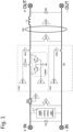
- FIG. 1 shows the basic architecture of the hybrid DC circuit breaker according to the present invention.
- a direct current circuit breaker comprising a positive supply line between a positive input terminal +IN and a positive output terminal +OUT, and a negative supply line between a negative input terminal -IN and a negative output terminal -OUT, for connecting a direct current load to a supply.
- a series connection of a first galvanic separation switch GSR1 and a bypass switch BYP1 is present in the positive supply line, and a second galvanic separation switch GSR2 in the negative supply line.
- a semiconductor switch element POWER1 is connected parallel to the bypass switch BYP1.
- the hybrid switch part is shown in the dashed line block with designation '+POLE', and comprises the first galvanic separation switch GSR1, the bypass switch BYP1 and semiconductor switch element POWER1.
- the first and second galvanic separation switch GSR1, GSR2, the bypass switch BYP1 and the semiconductor switch element POWER1 are controlled using a processing unit 5.
- the processing unit 5 is provided with various functional blocks, including but not limited to a power supply, control unit, communication unit and user interface, which allow to provide the functionalities of remote monitoring, remote parameterization, event depending parameterization, remote control, communication/logging, protection for overcurrent, short circuit, over-temperature, fault current, and arc-fault, energy measurement, programmable selectivity, fail safe and redundant design.
- the processing unit 5 may thus comprise circuitry for general internal power supply for all sub-circuits, for control of all the switch drivers (shown as signals RDR x , IDR y in the embodiments of Fig. 1 - 4 ), for functional behaviour program (including protocols for redundancy, remote control, remote parameterization, self-testing etc.), for a user interface, for communication (RS485, RF, Modbus, LAN, Wi-Fi etc.), for master to sub-distribution, slave to upper main-distribution, and for collecting all data from the detection means (DET i ) and processing the data.
- the processing unit 5 also executes software for the protection functions as e.g. overcurrent, short-circuit, earth-fault and arc-fault.
- the detection circuits as used (reference signs used in the Fig. 1-4 embodiments) and which are connected to the processing unit 5 are:
- the direct current circuit breaker comprises a series connected inductor L1 in the positive supply line, e.g. as indicated with one terminal connected to the positive output terminal +OUT.
- the inductor L1 has a special purpose. For DC-grids there is on many locations no high short circuit energy available and also no high short circuit capability of the breaker is needed. E.g. in solar power applications or when used behind a DC converter, 5kA would already be sufficient. Inductor L1 is dimensioned in such a way that it limits the change of current over time, dI/dt, resulting in sufficient time for the hybrid DC circuit breaker to disconnect reliable at a short circuit direct at the output of the hybrid DC circuit breaker. As an exemplary embodiment, if the total breaking time of the DC circuit breaker is e.g.
- the -POLE (indicated by dashed line in the embodiment of Fig. 1 , comprising the second galvanic separation switch GSR2) is not from itself protected for overcurrent and short circuit since this is not necessary in most DC grids. It is only galvanic separated by the galvanic separation switch GSR2 under control of a relay driver signal RDR2. If protection would be needed the same block as for the +POLE could be used for the -POLE.
- the direct current circuit breaker further comprises a second bypass switch in a series connection with the second galvanic separation switch GSR2.
- a DC earth leakage detection is based on e.g. core-balance measurement, with different possible detection principles, which are known as such to the person skilled in the art, e.g. using a hall-element, a core hysteresis saturation etc.
- this is indicated by an earth leakage measurement arrangement EL1 providing an earth leakage detection signal DET to the processing unit 5, and being arranged to monitor the positive supply line and negative supply line.
- Over current, short circuit, load current, current direction etc. can be measured by a low-ohmic shunt SH1, providing a current detection signal DET2 for the processing unit 5.
- a first current measurement arrangement is provided, which is connected to the processing unit 5 for measuring current flowing from the positive input terminal +IN to the positive supply line.
- a first voltage measurement arrangement DET1 may be present which is connected to the processing unit 5 and arranged to measure a voltage between the positive input terminal +IN and the negative input terminal -IN.
- a second voltage measurement arrangement DET4 may be furthermore present for measuring voltage between the positive output terminal +OUT and the negative output terminal -OUT.
- diodes D1 and D2 are added as indicated in the Figures directly connected between the input terminals +IN, -IN, and output terminals +OUT, -OUT, respectively. These are provided to avoid over-voltages on the inputs and outputs at switching off of the DC circuit breaker. In case the DC circuit breaker switches off, the energy in the wire-inductance will cause a peak voltage.
- the diodes D1 and D2 function as freewheel diode and will limit the overvoltage, depending on the direction of the current (energy from input to output or reverse).
- the direct current circuit breaker further comprises a first diode D1 having a cathode connected to the positive input terminal +IN and an anode connected to the negative input terminal -IN.
- the direct current circuit breaker further comprises a second diode D2 having a cathode connected to the positive output terminal +OUT and an anode connected to the negative output terminal -OUT.
- Fig. 7 shows a timing diagram of actuation of the various elements in the hybrid DC circuit breaker according to the present invention embodiments (with the horizontal axis being the time axis), and will be used here to explain the operational use of the DC circuit breaker embodiment of Fig. 1 . It is assumed that an input DC voltage Uin is present at the input terminals +IN, -IN, as indicated in the top line of the timing diagram of Fig. 7 , which on the second line shows the output voltage Uout on the output terminals +OUT, -OUT. After the ON command is given (third line, signal going 'high'), first the second galvanic separation switch GSR 2 in the -POLE will close (fourth line).
- the first galvanic separation switch GSR1 in the +POLE will close (fifth line).
- the ON switching itself is then done by the semiconductor switch element POWER1 (sixth line) which is in the load current forward direction and a short while later this is bypassed by the bypass switch BYP1 (seventh line). In the ON state it can be an advantage to switch off the semiconductor switch element POWER1.
- the sequence is just the other way around, as also indicated in the timing diagram of Fig. 7 .
- the semiconductor switch element POWER1 will execute the OFF switching after the bypass switch BYP1 has sufficient contact distance.
- the first and second galvanic separation switches GSR1 and GSR2 open to galvanic isolate the line +IN, -IN from the load side +OUT, -OUT. Please note that this sequence can be equal for both sourcing and sinking loads connected to the output terminals +OUT, -OUT.
- All galvanic separation switches GSRm and bypass switches BYPn as described in relation to the present invention embodiments are bi-stable and are driven by a short current pulse (e.g. using a relay driver signal RDR1 in the Fig. 1 embodiment). Energizing is done by connecting a charged capacitor from a relay driver circuits.
- the galvanic separation switches GSRm have a large contact distance for reliable isolation and may be slow, the bypass switches BYPn only have a small contact distance, but are very fast at opening.
- all bypass switches BYPn have an opening time which is shorter than an opening time of any one of the galvanic separation switches GSRm.
- a further problem which may occur in implementing DC circuit breakers is also that no small, ultra-fast, low-energizing, bi-stable relays are available on the market for the higher current range. If solutions for higher currents which are ultra-fast are made, these need a lot of energy for actuation. This makes a compact and economical design of a DC circuit breaker difficult.
- this problem is solved by splitting the high load current into paralleled modules. This way it is possible to use the available small bi-stable relays. Splitting the high load current into paralleled modules has also the advantage that redundancy and self-testing functionality is realized.
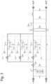
- Fig. 2 shows the architecture of an embodiment of the present invention hybrid DC circuit breaker for higher load currents and with redundancy. If one pole (+POLE in embodiment of Fig. 1 ) is not able to carry all the needed load current, a second pole (or third or more) can be paralleled, as shown in the embodiment of Fig. 2 by using +POLE1, +POLE2, +POLE3. Of course the current distribution between poles is relevant, but this can be controlled by properly selecting the internal wiring and contact materials. Also the shunt resistance SH2, SH3, SH4 in every pole +POLE1, +POLE2, +POLE3 helps to get an acceptable current distribution through the poles.
- the direct current circuit breaker thus further comprises an additional galvanic separation switch GSR3; GSR4 connected in series to each of the at least one additional bypass switch BYP2; BYP3.
- the poles +POLEn can be switched simultaneously or independently by the processing unit 5, using the associated driver signal pairs RDR x ; IDRy as shown in Fig. 2 .
- one pole +POLEn could be designed so that it's able to disconnect the overcurrent or short circuit at its own. In that case the timing behavior and current distribution between poles +POLEn is not critical. It is also possible to divide overcurrent and short circuit currents between more poles +POLEn. This makes a smaller design of the semiconductor switch element POWER n (IGBT power modules) possible.
- the current distribution between poles +POLEn at a short circuit is, after opening of the bypass switch BYPn, determined by the properties of the semiconductor switch element POWER n (specifically the IGBT's) in each of both other poles +POLEn.
- bypass switches BYPn and galvanic separation switches GSRm are advantageously small, ultra-fast, low-energizing and bi-stable which makes an economical design possible.
- Another advantage is also that an extra pole +POLEn can be added for redundancy. If one pole is able to carry e.g. 100A load current and the maximum load current is 200A, it is possible to disconnect one of the three poles +POLEn and change between poles +POLEn. If one pole +POLEn becomes defective in this situation it is possible to send a message to a maintenance engineer to replace the DC circuit breaker. It is also possible to control the temperature and ageing between the different poles +POLEn by regular changing from pole to another pole or connecting three poles in parallel.
- Self-testing of a redundant pole +POLEn is also very easy: the semiconductor switch element POWER n , bypass switch BYPn and galvanic separation switch GSRm of one pole +POLEn can be switched ON and OFF without interruption of the load current.
- the direct current circuit breaker in a further embodiment comprises a bypass current measurement arrangement for each of an associated bypass switch (BYPn).
- BYPn bypass switch
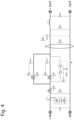
- the embodiment as shown in the schematic diagram of Fig. 3 has the same architecture as the embodiment shown in Fig. 2 , with an exception of the galvanic separation switches GSRm.
- the two or more galvanic separation switches GSRm from the different poles +POLEn are now combined in one galvanic separation switch GSR1 on the output line.
- the second galvanic separation switch GSR2 in the negative supply line can be combined in the same one galvanic separation switch GSR1.
- the first galvanic separation switch GSR1 and second galvanic separation switch GSR2 are combined and operated using a single relay driver signal RDR2 from the processing unit 5.
- the advantage is that it is cheaper to have one galvanic separation switch GSR1 and one relay driver signal RDR2 instead of four.
- a disadvantage may be that the redundancy from the Fig. 2 embodiment is no longer applicable for the galvanic separation switch GSR1.
- galvanic separation is in general only needed for maintenance situations, for normal protection and switching the hybrid direct current circuit breaker embodiments with a single galvanic separation switch GSR1 are in many applications acceptable.
- Another disadvantage may be that the galvanic separation switch GSR1 cannot be self-tested anymore.
- the combined galvanic separation switch GSR1 is too slow to shortly disconnect the load for a self-test.
- the direct current circuit breaker may in further embodiments further comprise an additional semiconductor switch element POWER2; POWER3 connected in parallel to each of the at least one additional bypass switch BYP2; BYP3, as shown in the embodiments of Fig. 2 and Fig. 3 .
- This allows applying the use of the switching timing described above with reference to Fig. 7 in each and every one of the poles +POLEn.
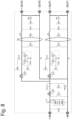
- the embodiment as shown in Fig. 4 provides an extra step in the reduction of components as compared to the embodiment shown in Fig. 3 .
- the galvanic separation switches are combined in a single galvanic separation switch GSR 1, but also the semiconductor switch elements POWER n are combined in a single version thereof (POWER1).
- the semiconductor switch element POWER1 now is connected in parallel to the series connection of each bypass switch BYP1, BYP2 and associated shunt resistor SH2, SH3 (in the Fig. 3 embodiment, each semiconductor switch element POWER n is connected in parallel to the associated bypass switch BYPn only).
- This embodiment can be described in a more generic embodiment as a direct current circuit breaker further comprising at least one additional bypass switch BYP2; BYP3 connected in parallel to the bypass switch BYP1, which feature is present in the embodiment of Fig. 4 , but also in the embodiments of Fig. 2 and Fig. 3 .
- semiconductor switch element POWER n normally is used for switching ON/OFF, so from an energy dissipation point of view it is possible to provide a single, combined semiconductor switch element POWER1. Also the short circuit disconnection is possible with a single semiconductor switch element POWER1, see also the description of the embodiment of Fig. 2 .
- a main advantage is that the embodiment according to Fig. 4 is more economic to implement than the embodiment according to Fig. 3 (or 2 ). A proper current distribution is still possible by choosing the right contact wiring and contact material.
- the shunt resistor SH2, SH3 is also allowing to have a proper current distribution.
- a variant of the Fig. 4 embodiment is possible with three or even more parallel current paths +POLE n .
- a possible disadvantage of this embodiment is that there is no redundancy in the semiconductor switch element POWER n (and the galvanic separation switches GSR n anymore, however, for applications where one single bypass switch BYP1 is not sufficient to carry the load current this embodiment provides an economical direct current circuit breaker.
- FIG. 5 An example of a direct current circuit breaker is shown in the schematic diagram of Fig. 5 .
- this version there are two or more output terminals +OUT2, -OUT2 (the other being referenced now as +OUT1 and - OUT1), connectable to the same input terminals +IN, -IN, processing unit 5 and input side shunt resistor SH1 using similar components for the circuit breaker functions in both branches.
- This hierarchy can be used as a complete DC-distribution system with flexible remote configurable functionality.
- This version can also be used in case of availability of a 4-wire cable to the sub-distribution board (two wires for +OUT1, -OUT1 and two wires for +OUT2, -OUT2).
- the embodiment relates to a direct current circuit breaker, wherein a primary circuit is formed by the positive supply line and the negative supply line, further comprising at least one secondary circuit connected to a secondary positive output terminal +OUT2 and to a secondary negative output terminal -OUT2, the at least one secondary circuit being a duplicate of the primary circuit. Similar components are then provided in both the primary circuit and the at least one secondary circuit (the two branches in the embodiment of Fig. 5 ), and the primary circuit and the at least one secondary circuit may be implemented in accordance with any one of the embodiments described herein.
- the semiconductor switch element POWER1 comprises a back-to-back circuit arrangement of two isolated gate bipolar transistors IGBT1, IGBT2, connected as indicated, and controlled by the input drive signal IDR1 originating from the processing unit 5.
- the semiconductor switch element POWER1 comprises a bridge rectifier d1-d4 and an isolated gate bipolar transistor IGBT3, which is controlled using an input drive signal IDR2 originating from the processing unit.
- an overvoltage protection element VDR1 is connected in parallel to the bypass switch BYP1, resp. BYP2.
- these embodiments of the semiconductor switch element POWER n may comprise appropriate snubber circuitry to suppress voltage transients caused by a sudden interruption of current.
- the snubber circuitry is provided as a separate snubber capacitor SN1 connected to the emitters of the isolated gate bipolar transistors IGBT1, IGBT2, and in the embodiment of Fig. 6B provided as snubber circuit comprising a capacitor SN2, diode d5 and resistor R1.
- the output terminals +OUT i , -OUTi must be galvanic separated from the input +IN, -IN (as prescribed by the relevant standards for utility grids).
- the output terminals +OUT i , -OUT i see also the Fig. 5 embodiment it could be advantageous to combine the galvanic separation for all outputs for cost reasons.
- this is accomplished by relocating the first galvanic separation switches GSRn and the second galvanic separation switch GSR2 from the parallel current paths +POLE n , -POLE, to a mutual part of the positive supply line and negative supply line, respectively.
- the input terminals +IN, -IN and processing unit 5 connected to the positive supply line and negative supply line form a mutual part of the direct current circuit breaker, and in this embodiment, the mutual part further comprises one or more common galvanic separation switches GSR1, GSR2.
- the processing unit 5, first current measurement arrangement (using shunt resistor SH1), first voltage measurement arrangement DET1, and (common) galvanic separation switches GSR1, GSR2 are directly connected in this mutual part.
- the common galvanic separation switches GSR1, GSR2 may be controlled by a single relay driver signal RDR1 as shown in Fig. 8 .
- the separate branches to the first and second output terminal pairs +OUT1, -OUT1, +OUT2, -OUT2 are then implemented using similar components.
- a normal ON/OFF switching of loads connected to the direct current circuit breaker is thus done in this embodiment using the hybrid switch part (bypass switch BYPn and semiconductor switch element POWER n ) of each parallel current branch. If maintenance is needed or e.g. in case of protection for over currents or earth faults in one of the parallel current branches, the common galvanic separation relays GSR1, GSR2 can be opened (under control of processing unit 5) as an extra safety measure.
- an output short circuit switch OSCS i is provided between each output terminal pair +OUT i , -OUT i .
- the output short circuit switches (in the embodiments of Fig. 8 OSCS1 and OSCS2) can be implemented using traditional relays, under control of a further relay driver signal (RDR3 and RDR5, respectively in the embodiment of Fig. 8 ) originating from the processing unit 5.
- the output short circuit switches OSCS i can be implemented using silicon (semiconductor) switches.
Landscapes
- Engineering & Computer Science (AREA)
- Power Engineering (AREA)
- Emergency Protection Circuit Devices (AREA)
Claims (12)
- Gleichstromunterbrecher, umfassendeine positive Versorgungsleitung zwischen einem positiven Eingangsanschluss (+IN) und einem positiven Ausgangsanschluss (+OUT) und eine negative Versorgungsleitung zwischen einem negativen Eingangsanschluss (-IN) und einem negativen Ausgangsanschluss (-OUT) zum Schalten einer Gleichstromlast zu einer Versorgung,eine Reihenschaltung eines ersten galvanischen Trennschalters (GSR1) und eines Überbrückungsschalters (BYP1) in der positiven Versorgungsleitung und eines zweiten galvanischen Trennschalters (GSR2) in der negativen Versorgungsleitung, undein Halbleiterschalterelement (POWER1), das zu dem Überbrückungsschalter (BYP1) parallel geschaltet ist, wobei der erste und der zweite galvanische Trennschalter (GSR1, GSR2), der Überbrückungsschalter (BYP1) und das Halbleiterschalterelement (POWER1) unter Verwendung einer Verarbeitungseinheit (5) gesteuert werden, dadurch gekennzeichnet, dassder Gleichstromunterbrecher ferner einen in Reihe geschalteten Induktor (L1) in der positiven Versorgungsleitung umfasst,, eine
erste Diode (D1) eine Kathode, die zu dem positiven Eingangsanschluss (+IN) geschaltet ist, und eine Anode, die zu dem negativen Eingangsanschluss (-IN) geschaltet ist, aufweist und eine zweite Diode (D2) eine Kathode, die zu dem positiven Ausgangsanschluss (+OUT) geschaltet ist, und eine Anode, die zu dem negativen Ausgangsanschluss (-OUT) geschaltet ist, aufweist. - Gleichstromunterbrecher nach Anspruch 1, ferner umfassend einen zweiten Überbrückungsschalter in einer Reihenschaltung mit dem zweiten galvanischen Trennschalter (GSR2).
- Gleichstromunterbrecher nach einem der Ansprüche 1 bis 2, ferner umfassend mindestens einen zusätzlichen Überbrückungsschalter (BYP2; BYP3), der zu dem Überbrückungsschalter (BYP1) parallel geschaltet ist, und ein zusätzliches Halbleiterschalterelement (POWER2; POWER3), das zu jedem des mindestens einen zusätzlichen Überbrückungsschalters (BYP2; BYP3) parallel geschaltet ist.
- Gleichstromunterbrecher nach Anspruch 3, ferner umfassend einen zusätzlichen galvanischen Trennschalter (GSR3; GSR4), der zu jedem des mindestens einen zusätzlichen Überbrückungsschalters (BYP2; BYP3) in Reihe geschaltet ist.
- Gleichstromunterbrecher nach Anspruch 3, wobei der erste galvanische Trennschalter (GSR1) und der zweite galvanische Trennschalter (GSR2) unter Verwendung eines einzelnen Relaistreibers (RDR2) kombiniert und betrieben werden.
- Gleichstromunterbrecher nach einem der Ansprüche 1 bis 5, wobei die Eingangsanschlüsse (+IN, -IN) und die Verarbeitungseinheit (5), die zu der positiven Versorgungsleitung und der negativen Versorgungsleitung geschaltet sind, einen gegenseitigen Teil des Gleichstromunterbrechers ausbilden, der gegenseitige Teil ferner umfassend einen oder mehrere gemeinsame galvanische Trennschalter (GSR1, GSR2).
- Gleichstromunterbrecher nach einem der Ansprüche 1 bis 6, ferner umfassend einen Ausgangskurzschlussschalter (OSCSi), der zwischen dem positiven Ausgangsanschluss (+OUTi) und dem negative Ausgangsanschluss (-OUTi) geschaltet ist.
- Gleichstromunterbrecher nach einem der Ansprüche 1 bis 7, wobei alle Überbrückungsschalter (BYPn) eine Öffnungszeit, die kürzer als eine Öffnungszeit eines beliebigen der galvanischen Trennschalter (GSRm) ist, aufweisen.
- Gleichstromunterbrecher nach einem der Ansprüche 1 bis 8, ferner umfassend eine erste Strommessanordnung, die zu der Verarbeitungseinheit (5) zum Messen von Strom, der von dem positiven Eingangsanschluss (+IN) zu der positiven Versorgungsleitung fließt, geschaltet ist.
- Gleichstromunterbrecher nach einem der Ansprüche 1 bis 9, ferner umfassend eine erste Spannungsmessanordnung (DET1), die zu der Verarbeitungseinheit (5) geschaltet und angeordnet ist, um eine Spannung zwischen dem positiven Eingangsanschluss (+IN) und dem negativen Eingangsanschluss (-IN) zu messen.
- Gleichstromunterbrecher nach einem der Ansprüche 1 bis 10, ferner umfassend eine Erdschlussmessanordnung (EL1), die zu der Verarbeitungseinheit (5) geschaltet und angeordnet ist, um die positive Versorgungsleitung und die negative Versorgungsleitung zu überwachen.
- Gleichstromunterbrecher nach einem der Ansprüche 1 bis 11, ferner umfassend eine zweite Spannungsmessanordnung (DET4) zum Messen von Spannung zwischen dem positiven Ausgangsanschluss (+OUT) und dem negativen Ausgangsanschluss (-OUT).
Applications Claiming Priority (2)
| Application Number | Priority Date | Filing Date | Title |
|---|---|---|---|
| GBGB1610901.9A GB201610901D0 (en) | 2016-06-22 | 2016-06-22 | Hybrid DC circuit breaker |
| PCT/EP2017/064797 WO2017220443A1 (en) | 2016-06-22 | 2017-06-16 | Hybrid dc circuit breaker |
Publications (2)
| Publication Number | Publication Date |
|---|---|
| EP3475963A1 EP3475963A1 (de) | 2019-05-01 |
| EP3475963B1 true EP3475963B1 (de) | 2023-11-01 |
Family
ID=56895064
Family Applications (1)
| Application Number | Title | Priority Date | Filing Date |
|---|---|---|---|
| EP17730485.4A Active EP3475963B1 (de) | 2016-06-22 | 2017-06-16 | Hybrider gleichstromschutzschalter |
Country Status (6)
| Country | Link |
|---|---|
| US (1) | US11322926B2 (de) |
| EP (1) | EP3475963B1 (de) |
| CN (1) | CN109314004A (de) |
| GB (1) | GB201610901D0 (de) |
| WO (1) | WO2017220443A1 (de) |
| ZA (1) | ZA201808628B (de) |
Families Citing this family (36)
| Publication number | Priority date | Publication date | Assignee | Title |
|---|---|---|---|---|
| LU93345B1 (de) * | 2016-12-08 | 2018-06-08 | Phoenix Contact Gmbh & Co Kg Intellectual Property Licenses & Standards | Schutzanordnung von elektrischen Verbrauchern und deren Anschlussleitungen vor Überstrom |
| CN111093891B (zh) * | 2017-04-27 | 2022-08-02 | 磁转换技术全球私人有限公司 | 具有至少一个传感器布置和消磁能力的磁耦合装置 |
| US10903030B2 (en) | 2017-04-27 | 2021-01-26 | Magswitch Technology Worldwide Pty Ltd. | Variable field magnetic couplers and methods for engaging a ferromagnetic workpiece |
| DE102018101309A1 (de) * | 2018-01-22 | 2019-07-25 | Eaton Intelligent Power Limited | Gleichstrom-Schutzschaltgerät |
| DE102018101312A1 (de) * | 2018-01-22 | 2019-07-25 | Eaton Intelligent Power Limited | Elektrische Schutzschaltungsanordnung |
| JP7115127B2 (ja) * | 2018-08-06 | 2022-08-09 | 富士電機株式会社 | スイッチ装置 |
| US11916375B2 (en) * | 2018-11-19 | 2024-02-27 | Powersecure, Inc. | Fault current limiter for energy storage systems |
| GB2579637A (en) * | 2018-12-07 | 2020-07-01 | Eaton Intelligent Power Ltd | Circuit breaker |
| CN111727487B (zh) * | 2019-01-21 | 2022-09-30 | 伊顿智能动力有限公司 | 直流电断路器 |
| CN109787200A (zh) * | 2019-02-20 | 2019-05-21 | 中国电力科学研究院有限公司 | 受端为lcc-vsc混联型的直流输电系统的断路器及其使用方法 |
| GB2581992A (en) | 2019-03-06 | 2020-09-09 | Eaton Intelligent Power Ltd | Circuit breaker |
| CN209929952U (zh) * | 2019-03-21 | 2020-01-10 | 许继集团有限公司 | 一种新型直流断路器 |
| DE102019203983B4 (de) | 2019-03-22 | 2020-10-08 | Siemens Aktiengesellschaft | Gleichspannungsschalter |
| EP3925048A1 (de) | 2019-03-29 | 2021-12-22 | Siemens Aktiengesellschaft | Elektrisches netzwerk |
| DE102019109200B4 (de) * | 2019-04-08 | 2024-03-07 | Infineon Technologies Ag | Halbleitervorrichtungen mit nicht-galvanischer verbindung |
| US10665398B1 (en) * | 2019-09-23 | 2020-05-26 | GM Global Technology Operations LLC | Direct current solid-state switch |
| EP3799306A1 (de) * | 2019-09-27 | 2021-03-31 | Siemens Aktiengesellschaft | Elektronischer schutzschalter |
| DE102019134212A1 (de) * | 2019-12-12 | 2021-06-17 | Bayerische Motoren Werke Aktiengesellschaft | Fahrzeug mit Energiespeichermodul |
| CN113224729B (zh) | 2020-01-21 | 2025-01-21 | 台达电子企业管理(上海)有限公司 | 直流母线过流保护电路与双向变换器 |
| CN112840517B (zh) * | 2020-06-15 | 2023-07-04 | 香港应用科技研究院有限公司 | 用于低压直流(lvdc)电网的电气保护装置 |
| US11070045B1 (en) * | 2020-06-15 | 2021-07-20 | Hong Kong Applied Science and Technology Research Institute Company Limited | Electrical protective device for low-voltage direct current (LVDC) network |
| CN112086943B (zh) * | 2020-09-02 | 2022-05-24 | 东南大学 | 一种主动式故障限流电路及全固态直流断路器 |
| DE102020132405A1 (de) | 2020-12-07 | 2022-06-09 | Bayerische Motoren Werke Aktiengesellschaft | Fahrzeug mit Energiespeichermodul |
| WO2022261520A1 (en) | 2021-06-11 | 2022-12-15 | Magswitch Technology, Inc. | Adjustable end-of-arm tool or fixture |
| BE1029566B1 (de) * | 2021-07-05 | 2023-02-06 | Phoenix Contact Gmbh & Co | Gleichspannungsschaltgerät mit Erdschlussschutz |
| CN114141572B (zh) * | 2021-11-03 | 2022-12-06 | 西安交通大学 | 电流转移式断路器 |
| CN118591860A (zh) * | 2022-02-03 | 2024-09-03 | 三菱电机株式会社 | 开闭装置及开闭装置的控制方法 |
| US11509233B1 (en) * | 2022-04-25 | 2022-11-22 | Resilient Power Systems, Inc. | Surge voltage protection for a power conversion system |
| CN114844003B (zh) * | 2022-05-05 | 2024-10-29 | 北京市科通电子继电器总厂有限公司 | 一种智能电源分配器控制方法和终端 |
| JP2024067609A (ja) * | 2022-11-07 | 2024-05-17 | ローム株式会社 | 半導体装置 |
| BE1031306B1 (de) * | 2023-01-31 | 2024-09-03 | Phoenix Contact Gmbh & Co | Gleichspannungsschaltgerät, insbesondere zum Unterbrechen eines Stromflusses, und Gleichspannungssystem |
| BE1031299B1 (de) * | 2023-01-31 | 2024-09-03 | Phoenix Contact Gmbh & Co | Gleichspannungsschaltgerät, insbesondere zum Unterbrechen eines Stromflusses, und Gleichspannungssystem |
| BE1031301B1 (de) * | 2023-01-31 | 2024-09-02 | Phoenix Contact Gmbh & Co | Schaltgerät zum elektrischen Ein- und Ausschalten einer mit einer Gleichspannungs-Versorgungseinrichtung verbindbaren elektrischen Last |
| GB2628123A (en) * | 2023-03-14 | 2024-09-18 | Eaton Intelligent Power Ltd | Switch circuit and power arrangement |
| US12469661B2 (en) | 2023-03-21 | 2025-11-11 | Siemens Industry, Inc. | DC solid-state circuit breaker with fail-safe redundancy via double power electronics and overvoltage protection |
| US12519303B2 (en) | 2023-09-22 | 2026-01-06 | Delta Electronics, Inc. | Hybrid circuit breaker and pre-charge control method |
Family Cites Families (21)
| Publication number | Priority date | Publication date | Assignee | Title |
|---|---|---|---|---|
| US6075684A (en) * | 1998-03-23 | 2000-06-13 | Electric Boat Corporation | Method and arrangement for direct current circuit interruption |
| EP1995818A1 (de) * | 2007-05-12 | 2008-11-26 | Huettinger Electronic Sp. z o. o | Schaltung und Verfahren zur Reduzierung der in einer Zuleitungsinduktivität gespeicherten elektrischen Energie zur schnellen Plasmalichtbogenlöschung |
| AT505801B1 (de) * | 2007-09-20 | 2012-09-15 | Siemens Ag | Verfahren zum betrieb eines elektronisch gesteuerten wechselrichters |
| JP5443749B2 (ja) * | 2007-12-26 | 2014-03-19 | ローム株式会社 | 昇圧型スイッチングレギュレータおよびその制御回路 |
| US20100019578A1 (en) * | 2008-07-26 | 2010-01-28 | Semikron Elektronik Gmbh & Co. Kg | Power Converter for Solar Electrical Current Installations and Method for Controlling it |
| FR2952470A1 (fr) | 2009-11-06 | 2011-05-13 | Schneider Electric Ind Sas | Disjoncteur limiteur de courant, dispositif de distribution electrique pourvu d'un tel disjoncteur limiteur et procede de limitation de courant |
| WO2011057675A1 (en) | 2009-11-16 | 2011-05-19 | Abb Technology Ag | Device and method to break the current of a power transmission or distribution line and current limiting arrangement |
| JP5594728B2 (ja) | 2010-07-23 | 2014-09-24 | 松尾博文 | 直流スイッチ |
| EP2469552B1 (de) | 2010-12-23 | 2014-02-26 | ABB Technology AG | Verfahren, Schutzschalter und Schalteinheit zum Abschalten von Hochspannungsgleichströmen |
| CN102497706B (zh) * | 2011-12-15 | 2014-06-25 | 成都芯源系统有限公司 | Led驱动装置和驱动方法以及控制器 |
| WO2013102879A1 (en) * | 2012-01-06 | 2013-07-11 | Koninklijke Philips Electronics N.V. | Power converter with separate buck and boost conversion circuits |
| CN103208855B (zh) * | 2012-01-17 | 2016-06-29 | 华为技术有限公司 | 一种不间断电源和dc-dc变换器 |
| US20150214732A1 (en) * | 2013-05-13 | 2015-07-30 | Kabushiki Kaisha Toshiba | Semiconductor circuit |
| US9947496B2 (en) | 2013-08-30 | 2018-04-17 | Eaton Industries (Netherlands) B.V. | Circuit breaker with hybrid switch |
| US9425188B2 (en) * | 2013-09-26 | 2016-08-23 | Texas Instruments Incorporated | Active ESD protection circuit with blocking diode |
| GB2527534A (en) * | 2014-06-24 | 2015-12-30 | Eaton Ind Netherlands Bv | Selective circuit breaker |
| US9647548B2 (en) * | 2015-03-13 | 2017-05-09 | Infineon Technologies Austria Ag | Method for operating a power converter circuit and power converter circuit |
| JP6187515B2 (ja) * | 2015-03-20 | 2017-08-30 | トヨタ自動車株式会社 | 電源システム |
| US9722506B2 (en) * | 2015-09-18 | 2017-08-01 | Power Integrations, Inc. | Limit-to-valley ratio circuitry in power converters |
| US11264902B2 (en) * | 2016-03-02 | 2022-03-01 | Analog Devices International Unlimited Company | Inductor current based mode control for buck-boost converters |
| CN105609344B (zh) | 2016-03-22 | 2019-06-11 | 国网天津市电力公司 | 一种混合式直流断路器拓扑结构 |
-
2016
- 2016-06-22 GB GBGB1610901.9A patent/GB201610901D0/en not_active Ceased
-
2017
- 2017-06-16 US US16/311,699 patent/US11322926B2/en active Active
- 2017-06-16 WO PCT/EP2017/064797 patent/WO2017220443A1/en not_active Ceased
- 2017-06-16 EP EP17730485.4A patent/EP3475963B1/de active Active
- 2017-06-16 CN CN201780038274.1A patent/CN109314004A/zh active Pending
-
2018
- 2018-12-20 ZA ZA2018/08628A patent/ZA201808628B/en unknown
Also Published As
| Publication number | Publication date |
|---|---|
| EP3475963A1 (de) | 2019-05-01 |
| GB201610901D0 (en) | 2016-08-03 |
| WO2017220443A1 (en) | 2017-12-28 |
| US11322926B2 (en) | 2022-05-03 |
| CN109314004A (zh) | 2019-02-05 |
| ZA201808628B (en) | 2023-04-26 |
| US20190334340A1 (en) | 2019-10-31 |
Similar Documents
| Publication | Publication Date | Title |
|---|---|---|
| EP3475963B1 (de) | Hybrider gleichstromschutzschalter | |
| KR101453631B1 (ko) | 고전압용 컨버터 | |
| CN107466434B (zh) | 控制不间断电源以清除短路负载的方法 | |
| CN208433908U (zh) | 电压源换流器模块和换流器 | |
| US20150372474A1 (en) | Circuit interruption device | |
| US10074972B2 (en) | System and method of controlling current-limiters in ring systems | |
| DK2926455T3 (en) | DEVICE FOR SWITCHING OF DC DIRECTIONS IN THE DEFINITIONS OF A DC TENSION | |
| CN101297448B (zh) | 换流站 | |
| WO2016092038A1 (en) | Dc electrical network | |
| CN112514192A (zh) | 交流/直流电转换装置 | |
| JP2023092522A (ja) | ハイブリッド回路遮断器 | |
| US11368084B2 (en) | Current converter unit, transmission installation having a current converter unit, and method for fault management in a current converter unit | |
| WO2015090365A1 (en) | Integrated series converter and circuit breaker in a power system | |
| US9893520B2 (en) | Switching device | |
| US10333313B2 (en) | Electrical assembly | |
| EP3084908B1 (de) | Schutzschalteranordnung | |
| RU2468486C2 (ru) | Устройство для передачи постоянного тока высокого напряжения | |
| EP2498360B1 (de) | Elektrisches Gleichstromsystem | |
| CN114514700B (zh) | 电子保护开关 | |
| CN110070999A (zh) | 电路断路器组合件 | |
| KR102691751B1 (ko) | 직류 시스템 보호 회로, 상기 직류 시스템 보호 회로를 포함하는 차단기 및 상기 직류 시스템 보호 회로를 포함하는 컨버터 시스템 | |
| WO2026087427A1 (en) | Circuit breaker with internal power supply | |
| RU75787U1 (ru) | Гибридное коммутационное устройство постоянного тока | |
| Carminati et al. | Overview on faults and protections in LVDC microgrids connected to the AC utility | |
| KR200469560Y1 (ko) | 소켓 아울렛 장치 |
Legal Events
| Date | Code | Title | Description |
|---|---|---|---|
| STAA | Information on the status of an ep patent application or granted ep patent |
Free format text: STATUS: UNKNOWN |
|
| STAA | Information on the status of an ep patent application or granted ep patent |
Free format text: STATUS: THE INTERNATIONAL PUBLICATION HAS BEEN MADE |
|
| PUAI | Public reference made under article 153(3) epc to a published international application that has entered the european phase |
Free format text: ORIGINAL CODE: 0009012 |
|
| STAA | Information on the status of an ep patent application or granted ep patent |
Free format text: STATUS: REQUEST FOR EXAMINATION WAS MADE |
|
| 17P | Request for examination filed |
Effective date: 20190108 |
|
| AK | Designated contracting states |
Kind code of ref document: A1 Designated state(s): AL AT BE BG CH CY CZ DE DK EE ES FI FR GB GR HR HU IE IS IT LI LT LU LV MC MK MT NL NO PL PT RO RS SE SI SK SM TR |
|
| AX | Request for extension of the european patent |
Extension state: BA ME |
|
| DAV | Request for validation of the european patent (deleted) | ||
| DAX | Request for extension of the european patent (deleted) | ||
| STAA | Information on the status of an ep patent application or granted ep patent |
Free format text: STATUS: EXAMINATION IS IN PROGRESS |
|
| 17Q | First examination report despatched |
Effective date: 20211014 |
|
| REG | Reference to a national code |
Ref country code: DE Ref legal event code: R079 Ipc: H01H0007100000 Ref country code: DE Ref legal event code: R079 Ref document number: 602017075972 Country of ref document: DE Free format text: PREVIOUS MAIN CLASS: H01H0009540000 Ipc: H01H0007100000 |
|
| RIC1 | Information provided on ipc code assigned before grant |
Ipc: H01H 83/20 20060101ALI20220428BHEP Ipc: H01H 71/10 20060101ALI20220428BHEP Ipc: H02H 3/087 20060101ALI20220428BHEP Ipc: H01H 33/59 20060101ALI20220428BHEP Ipc: H01H 9/54 20060101ALI20220428BHEP Ipc: H01H 7/10 20060101AFI20220428BHEP |
|
| GRAP | Despatch of communication of intention to grant a patent |
Free format text: ORIGINAL CODE: EPIDOSNIGR1 |
|
| STAA | Information on the status of an ep patent application or granted ep patent |
Free format text: STATUS: GRANT OF PATENT IS INTENDED |
|
| INTG | Intention to grant announced |
Effective date: 20230525 |
|
| P01 | Opt-out of the competence of the unified patent court (upc) registered |
Effective date: 20230521 |
|
| GRAS | Grant fee paid |
Free format text: ORIGINAL CODE: EPIDOSNIGR3 |
|
| GRAA | (expected) grant |
Free format text: ORIGINAL CODE: 0009210 |
|
| STAA | Information on the status of an ep patent application or granted ep patent |
Free format text: STATUS: THE PATENT HAS BEEN GRANTED |
|
| AK | Designated contracting states |
Kind code of ref document: B1 Designated state(s): AL AT BE BG CH CY CZ DE DK EE ES FI FR GB GR HR HU IE IS IT LI LT LU LV MC MK MT NL NO PL PT RO RS SE SI SK SM TR |
|
| REG | Reference to a national code |
Ref country code: GB Ref legal event code: FG4D |
|
| REG | Reference to a national code |
Ref country code: CH Ref legal event code: EP |
|
| REG | Reference to a national code |
Ref country code: IE Ref legal event code: FG4D |
|
| REG | Reference to a national code |
Ref country code: DE Ref legal event code: R096 Ref document number: 602017075972 Country of ref document: DE |
|
| REG | Reference to a national code |
Ref country code: NL Ref legal event code: FP |
|
| REG | Reference to a national code |
Ref country code: LT Ref legal event code: MG9D |
|
| PG25 | Lapsed in a contracting state [announced via postgrant information from national office to epo] |
Ref country code: GR Free format text: LAPSE BECAUSE OF FAILURE TO SUBMIT A TRANSLATION OF THE DESCRIPTION OR TO PAY THE FEE WITHIN THE PRESCRIBED TIME-LIMIT Effective date: 20240202 |
|
| PG25 | Lapsed in a contracting state [announced via postgrant information from national office to epo] |
Ref country code: IS Free format text: LAPSE BECAUSE OF FAILURE TO SUBMIT A TRANSLATION OF THE DESCRIPTION OR TO PAY THE FEE WITHIN THE PRESCRIBED TIME-LIMIT Effective date: 20240301 |
|
| PG25 | Lapsed in a contracting state [announced via postgrant information from national office to epo] |
Ref country code: LT Free format text: LAPSE BECAUSE OF FAILURE TO SUBMIT A TRANSLATION OF THE DESCRIPTION OR TO PAY THE FEE WITHIN THE PRESCRIBED TIME-LIMIT Effective date: 20231101 |
|
| REG | Reference to a national code |
Ref country code: AT Ref legal event code: MK05 Ref document number: 1628201 Country of ref document: AT Kind code of ref document: T Effective date: 20231101 |
|
| PG25 | Lapsed in a contracting state [announced via postgrant information from national office to epo] |
Ref country code: AT Free format text: LAPSE BECAUSE OF FAILURE TO SUBMIT A TRANSLATION OF THE DESCRIPTION OR TO PAY THE FEE WITHIN THE PRESCRIBED TIME-LIMIT Effective date: 20231101 |
|
| PG25 | Lapsed in a contracting state [announced via postgrant information from national office to epo] |
Ref country code: ES Free format text: LAPSE BECAUSE OF FAILURE TO SUBMIT A TRANSLATION OF THE DESCRIPTION OR TO PAY THE FEE WITHIN THE PRESCRIBED TIME-LIMIT Effective date: 20231101 |
|
| PG25 | Lapsed in a contracting state [announced via postgrant information from national office to epo] |
Ref country code: LT Free format text: LAPSE BECAUSE OF FAILURE TO SUBMIT A TRANSLATION OF THE DESCRIPTION OR TO PAY THE FEE WITHIN THE PRESCRIBED TIME-LIMIT Effective date: 20231101 Ref country code: IS Free format text: LAPSE BECAUSE OF FAILURE TO SUBMIT A TRANSLATION OF THE DESCRIPTION OR TO PAY THE FEE WITHIN THE PRESCRIBED TIME-LIMIT Effective date: 20240301 Ref country code: GR Free format text: LAPSE BECAUSE OF FAILURE TO SUBMIT A TRANSLATION OF THE DESCRIPTION OR TO PAY THE FEE WITHIN THE PRESCRIBED TIME-LIMIT Effective date: 20240202 Ref country code: ES Free format text: LAPSE BECAUSE OF FAILURE TO SUBMIT A TRANSLATION OF THE DESCRIPTION OR TO PAY THE FEE WITHIN THE PRESCRIBED TIME-LIMIT Effective date: 20231101 Ref country code: BG Free format text: LAPSE BECAUSE OF FAILURE TO SUBMIT A TRANSLATION OF THE DESCRIPTION OR TO PAY THE FEE WITHIN THE PRESCRIBED TIME-LIMIT Effective date: 20240201 Ref country code: AT Free format text: LAPSE BECAUSE OF FAILURE TO SUBMIT A TRANSLATION OF THE DESCRIPTION OR TO PAY THE FEE WITHIN THE PRESCRIBED TIME-LIMIT Effective date: 20231101 Ref country code: PT Free format text: LAPSE BECAUSE OF FAILURE TO SUBMIT A TRANSLATION OF THE DESCRIPTION OR TO PAY THE FEE WITHIN THE PRESCRIBED TIME-LIMIT Effective date: 20240301 |
|
| PG25 | Lapsed in a contracting state [announced via postgrant information from national office to epo] |
Ref country code: SE Free format text: LAPSE BECAUSE OF FAILURE TO SUBMIT A TRANSLATION OF THE DESCRIPTION OR TO PAY THE FEE WITHIN THE PRESCRIBED TIME-LIMIT Effective date: 20231101 Ref country code: RS Free format text: LAPSE BECAUSE OF FAILURE TO SUBMIT A TRANSLATION OF THE DESCRIPTION OR TO PAY THE FEE WITHIN THE PRESCRIBED TIME-LIMIT Effective date: 20231101 Ref country code: PL Free format text: LAPSE BECAUSE OF FAILURE TO SUBMIT A TRANSLATION OF THE DESCRIPTION OR TO PAY THE FEE WITHIN THE PRESCRIBED TIME-LIMIT Effective date: 20231101 Ref country code: NO Free format text: LAPSE BECAUSE OF FAILURE TO SUBMIT A TRANSLATION OF THE DESCRIPTION OR TO PAY THE FEE WITHIN THE PRESCRIBED TIME-LIMIT Effective date: 20240201 Ref country code: LV Free format text: LAPSE BECAUSE OF FAILURE TO SUBMIT A TRANSLATION OF THE DESCRIPTION OR TO PAY THE FEE WITHIN THE PRESCRIBED TIME-LIMIT Effective date: 20231101 Ref country code: HR Free format text: LAPSE BECAUSE OF FAILURE TO SUBMIT A TRANSLATION OF THE DESCRIPTION OR TO PAY THE FEE WITHIN THE PRESCRIBED TIME-LIMIT Effective date: 20231101 |
|
| PG25 | Lapsed in a contracting state [announced via postgrant information from national office to epo] |
Ref country code: DK Free format text: LAPSE BECAUSE OF FAILURE TO SUBMIT A TRANSLATION OF THE DESCRIPTION OR TO PAY THE FEE WITHIN THE PRESCRIBED TIME-LIMIT Effective date: 20231101 |
|
| PG25 | Lapsed in a contracting state [announced via postgrant information from national office to epo] |
Ref country code: CZ Free format text: LAPSE BECAUSE OF FAILURE TO SUBMIT A TRANSLATION OF THE DESCRIPTION OR TO PAY THE FEE WITHIN THE PRESCRIBED TIME-LIMIT Effective date: 20231101 |
|
| PG25 | Lapsed in a contracting state [announced via postgrant information from national office to epo] |
Ref country code: SK Free format text: LAPSE BECAUSE OF FAILURE TO SUBMIT A TRANSLATION OF THE DESCRIPTION OR TO PAY THE FEE WITHIN THE PRESCRIBED TIME-LIMIT Effective date: 20231101 |
|
| PG25 | Lapsed in a contracting state [announced via postgrant information from national office to epo] |
Ref country code: SM Free format text: LAPSE BECAUSE OF FAILURE TO SUBMIT A TRANSLATION OF THE DESCRIPTION OR TO PAY THE FEE WITHIN THE PRESCRIBED TIME-LIMIT Effective date: 20231101 Ref country code: SK Free format text: LAPSE BECAUSE OF FAILURE TO SUBMIT A TRANSLATION OF THE DESCRIPTION OR TO PAY THE FEE WITHIN THE PRESCRIBED TIME-LIMIT Effective date: 20231101 Ref country code: RO Free format text: LAPSE BECAUSE OF FAILURE TO SUBMIT A TRANSLATION OF THE DESCRIPTION OR TO PAY THE FEE WITHIN THE PRESCRIBED TIME-LIMIT Effective date: 20231101 Ref country code: EE Free format text: LAPSE BECAUSE OF FAILURE TO SUBMIT A TRANSLATION OF THE DESCRIPTION OR TO PAY THE FEE WITHIN THE PRESCRIBED TIME-LIMIT Effective date: 20231101 Ref country code: DK Free format text: LAPSE BECAUSE OF FAILURE TO SUBMIT A TRANSLATION OF THE DESCRIPTION OR TO PAY THE FEE WITHIN THE PRESCRIBED TIME-LIMIT Effective date: 20231101 Ref country code: CZ Free format text: LAPSE BECAUSE OF FAILURE TO SUBMIT A TRANSLATION OF THE DESCRIPTION OR TO PAY THE FEE WITHIN THE PRESCRIBED TIME-LIMIT Effective date: 20231101 |
|
| REG | Reference to a national code |
Ref country code: DE Ref legal event code: R097 Ref document number: 602017075972 Country of ref document: DE |
|
| PLBE | No opposition filed within time limit |
Free format text: ORIGINAL CODE: 0009261 |
|
| STAA | Information on the status of an ep patent application or granted ep patent |
Free format text: STATUS: NO OPPOSITION FILED WITHIN TIME LIMIT |
|
| 26N | No opposition filed |
Effective date: 20240802 |
|
| PG25 | Lapsed in a contracting state [announced via postgrant information from national office to epo] |
Ref country code: SI Free format text: LAPSE BECAUSE OF FAILURE TO SUBMIT A TRANSLATION OF THE DESCRIPTION OR TO PAY THE FEE WITHIN THE PRESCRIBED TIME-LIMIT Effective date: 20231101 |
|
| PG25 | Lapsed in a contracting state [announced via postgrant information from national office to epo] |
Ref country code: SI Free format text: LAPSE BECAUSE OF FAILURE TO SUBMIT A TRANSLATION OF THE DESCRIPTION OR TO PAY THE FEE WITHIN THE PRESCRIBED TIME-LIMIT Effective date: 20231101 |
|
| PG25 | Lapsed in a contracting state [announced via postgrant information from national office to epo] |
Ref country code: MC Free format text: LAPSE BECAUSE OF FAILURE TO SUBMIT A TRANSLATION OF THE DESCRIPTION OR TO PAY THE FEE WITHIN THE PRESCRIBED TIME-LIMIT Effective date: 20231101 |
|
| REG | Reference to a national code |
Ref country code: CH Ref legal event code: PL |
|
| PG25 | Lapsed in a contracting state [announced via postgrant information from national office to epo] |
Ref country code: LU Free format text: LAPSE BECAUSE OF NON-PAYMENT OF DUE FEES Effective date: 20240616 |
|
| PG25 | Lapsed in a contracting state [announced via postgrant information from national office to epo] |
Ref country code: IE Free format text: LAPSE BECAUSE OF NON-PAYMENT OF DUE FEES Effective date: 20240616 |
|
| PG25 | Lapsed in a contracting state [announced via postgrant information from national office to epo] |
Ref country code: CH Free format text: LAPSE BECAUSE OF NON-PAYMENT OF DUE FEES Effective date: 20240630 Ref country code: BE Free format text: LAPSE BECAUSE OF NON-PAYMENT OF DUE FEES Effective date: 20240630 |
|
| REG | Reference to a national code |
Ref country code: BE Ref legal event code: MM Effective date: 20240630 |
|
| PGFP | Annual fee paid to national office [announced via postgrant information from national office to epo] |
Ref country code: NL Payment date: 20250520 Year of fee payment: 9 |
|
| PGFP | Annual fee paid to national office [announced via postgrant information from national office to epo] |
Ref country code: DE Payment date: 20250520 Year of fee payment: 9 |
|
| PGFP | Annual fee paid to national office [announced via postgrant information from national office to epo] |
Ref country code: GB Payment date: 20250520 Year of fee payment: 9 |
|
| PGFP | Annual fee paid to national office [announced via postgrant information from national office to epo] |
Ref country code: IT Payment date: 20250520 Year of fee payment: 9 |
|
| PGFP | Annual fee paid to national office [announced via postgrant information from national office to epo] |
Ref country code: FR Payment date: 20250520 Year of fee payment: 9 |
|
| PG25 | Lapsed in a contracting state [announced via postgrant information from national office to epo] |
Ref country code: FI Free format text: LAPSE BECAUSE OF FAILURE TO SUBMIT A TRANSLATION OF THE DESCRIPTION OR TO PAY THE FEE WITHIN THE PRESCRIBED TIME-LIMIT Effective date: 20231101 |
|
| PG25 | Lapsed in a contracting state [announced via postgrant information from national office to epo] |
Ref country code: CY Free format text: LAPSE BECAUSE OF FAILURE TO SUBMIT A TRANSLATION OF THE DESCRIPTION OR TO PAY THE FEE WITHIN THE PRESCRIBED TIME-LIMIT; INVALID AB INITIO Effective date: 20170616 |
|
| PG25 | Lapsed in a contracting state [announced via postgrant information from national office to epo] |
Ref country code: HU Free format text: LAPSE BECAUSE OF FAILURE TO SUBMIT A TRANSLATION OF THE DESCRIPTION OR TO PAY THE FEE WITHIN THE PRESCRIBED TIME-LIMIT; INVALID AB INITIO Effective date: 20170616 |