EP3477362A1 - Modulateur électro-optique - Google Patents
Modulateur électro-optique Download PDFInfo
- Publication number
- EP3477362A1 EP3477362A1 EP16909229.3A EP16909229A EP3477362A1 EP 3477362 A1 EP3477362 A1 EP 3477362A1 EP 16909229 A EP16909229 A EP 16909229A EP 3477362 A1 EP3477362 A1 EP 3477362A1
- Authority
- EP
- European Patent Office
- Prior art keywords
- electrode
- layer
- electro
- modulator
- optic modulator
- Prior art date
- Legal status (The legal status is an assumption and is not a legal conclusion. Google has not performed a legal analysis and makes no representation as to the accuracy of the status listed.)
- Granted
Links
Images
Classifications
-
- G—PHYSICS
- G02—OPTICS
- G02F—OPTICAL DEVICES OR ARRANGEMENTS FOR THE CONTROL OF LIGHT BY MODIFICATION OF THE OPTICAL PROPERTIES OF THE MEDIA OF THE ELEMENTS INVOLVED THEREIN; NON-LINEAR OPTICS; FREQUENCY-CHANGING OF LIGHT; OPTICAL LOGIC ELEMENTS; OPTICAL ANALOGUE/DIGITAL CONVERTERS
- G02F1/00—Devices or arrangements for the control of the intensity, colour, phase, polarisation or direction of light arriving from an independent light source, e.g. switching, gating or modulating; Non-linear optics
- G02F1/01—Devices or arrangements for the control of the intensity, colour, phase, polarisation or direction of light arriving from an independent light source, e.g. switching, gating or modulating; Non-linear optics for the control of the intensity, phase, polarisation or colour
- G02F1/015—Devices or arrangements for the control of the intensity, colour, phase, polarisation or direction of light arriving from an independent light source, e.g. switching, gating or modulating; Non-linear optics for the control of the intensity, phase, polarisation or colour based on semiconductor elements having potential barriers, e.g. having a PN or PIN junction
- G02F1/025—Devices or arrangements for the control of the intensity, colour, phase, polarisation or direction of light arriving from an independent light source, e.g. switching, gating or modulating; Non-linear optics for the control of the intensity, phase, polarisation or colour based on semiconductor elements having potential barriers, e.g. having a PN or PIN junction in an optical waveguide structure
-
- G—PHYSICS
- G02—OPTICS
- G02F—OPTICAL DEVICES OR ARRANGEMENTS FOR THE CONTROL OF LIGHT BY MODIFICATION OF THE OPTICAL PROPERTIES OF THE MEDIA OF THE ELEMENTS INVOLVED THEREIN; NON-LINEAR OPTICS; FREQUENCY-CHANGING OF LIGHT; OPTICAL LOGIC ELEMENTS; OPTICAL ANALOGUE/DIGITAL CONVERTERS
- G02F1/00—Devices or arrangements for the control of the intensity, colour, phase, polarisation or direction of light arriving from an independent light source, e.g. switching, gating or modulating; Non-linear optics
- G02F1/01—Devices or arrangements for the control of the intensity, colour, phase, polarisation or direction of light arriving from an independent light source, e.g. switching, gating or modulating; Non-linear optics for the control of the intensity, phase, polarisation or colour
- G02F1/015—Devices or arrangements for the control of the intensity, colour, phase, polarisation or direction of light arriving from an independent light source, e.g. switching, gating or modulating; Non-linear optics for the control of the intensity, phase, polarisation or colour based on semiconductor elements having potential barriers, e.g. having a PN or PIN junction
-
- G—PHYSICS
- G02—OPTICS
- G02F—OPTICAL DEVICES OR ARRANGEMENTS FOR THE CONTROL OF LIGHT BY MODIFICATION OF THE OPTICAL PROPERTIES OF THE MEDIA OF THE ELEMENTS INVOLVED THEREIN; NON-LINEAR OPTICS; FREQUENCY-CHANGING OF LIGHT; OPTICAL LOGIC ELEMENTS; OPTICAL ANALOGUE/DIGITAL CONVERTERS
- G02F1/00—Devices or arrangements for the control of the intensity, colour, phase, polarisation or direction of light arriving from an independent light source, e.g. switching, gating or modulating; Non-linear optics
- G02F1/01—Devices or arrangements for the control of the intensity, colour, phase, polarisation or direction of light arriving from an independent light source, e.g. switching, gating or modulating; Non-linear optics for the control of the intensity, phase, polarisation or colour
- G02F1/015—Devices or arrangements for the control of the intensity, colour, phase, polarisation or direction of light arriving from an independent light source, e.g. switching, gating or modulating; Non-linear optics for the control of the intensity, phase, polarisation or colour based on semiconductor elements having potential barriers, e.g. having a PN or PIN junction
- G02F1/0151—Devices or arrangements for the control of the intensity, colour, phase, polarisation or direction of light arriving from an independent light source, e.g. switching, gating or modulating; Non-linear optics for the control of the intensity, phase, polarisation or colour based on semiconductor elements having potential barriers, e.g. having a PN or PIN junction modulating the refractive index
Definitions
- the present invention relates to the field of communications technologies, and in particular, to an electro-optic modulator.
- the silicon photonics technology has been widely studied in the industry and academia, and various functional components are successively developed, and include a low-loss silicon waveguide, a beam splitter/combiner, an electro-optic modulator, a filter, a wavelength division multiplexer/demultiplexer, a photoelectric detector, and the like.
- the silicon photonics technology includes the following advantages: A silicon waveguide has a large refractive index difference, so that a size of the waveguide can be reduced to a submicron level, and waveguide bend at a micrometer level can be implemented. Therefore, the silicon photonics technology can implement integration of higher-density components.
- a silicon-waveguide-based optical component may be fully processed by using a mature CMOS technique, and generated in batches at low costs.
- Monolithic integration may be performed on a silicon-waveguide-based optical component and a microelectronic circuit, so that a more complex system can be created, and a more complex function can be completed.
- a silicon-based modulator with low drive pressure, high integration, and a high modulation rate is a key enabling technology.
- An O/E co-package solution of a high-density multi-channel integrated electro-optic modulator is also required in a future application scenario such as an optical backplane and a high-capacity cluster, and the like.
- An integrated multi-channel electro-optic modulator is a key enabling technology for O/E co-package.
- an optical component and a photonic chip with a complex function can be manufactured in batches at low costs by using a mature silicon technique.
- a silicon-based electro-optic modulator that is on the basis of a silicon technique has potential to implement high-density multi-channel integration.
- the high-density multi-channel integration needs to be compatible with a high-density packaging layout, to implement high-speed electro-packaging of a high-density multi-channel modulator.
- the high-density multi-channel modulator and a high-speed high-density electro-packaging technology and solution are also required by future multi-channel high-capacity high-density optical modules such as CFP8 and CFP16.
- the present invention provides an electro-optic modulator, to further improve integration of the electro-optic modulator, and effectively reduce high-density packaging layout difficulty and cabling pressure.
- the present invention provides an electro-optic modulator, and the electro-optic modulator includes an input waveguide, a beam splitter connected to the input waveguide, a modulation arm that is disposed on each branch of the beam splitter and that is configured to modulate a signal, a beam combiner that is connected to each branch of the beam splitter and that is configured to combine signals, and an output waveguide connected to the beam combiner.
- Each modulation arm is correspondingly disposed with a double-layer electrode
- a first layer electrode of the double-layer electrode is a high-frequency traveling wave electrode that is configured to change carrier concentration in the modulation arm
- a second layer electrode is a direct current electrode having an inductor function
- each modulation arm is disposed with a double-layer electrode, a first layer electrode of the double-layer electrode uses a high-frequency traveling wave electrode, and a second layer electrode uses a direct current electrode that can form an inductor.
- the electro-optic modulator has some functions of a bias tee, integration of the electro-optic modulator is improved, and an external connection structure of the electro-optic modulator is reduced, so that the integration of the electro-optic modulator can be further improved without affecting performance of the electro-optic modulator, high-density packaging layout difficulty and cabling pressure can be effectively reduced, and cabling and packaging of a multi-channel high-speed signal on a base board can be implemented.
- a capacitor that is disposed on a side of the input waveguide and that is corresponding to each modulation arm is further included.
- the electro-optic modulator has a modulator high-frequency signal input end, one end of the capacitor is connected to the modulator high-frequency signal input end of the electro-optic modulator, the other end of the capacitor is connected to the high-frequency traveling wave electrode, and the capacitor and the inductor in the second layer electrode are both connected to the high-frequency traveling wave electrode, to form a bias tee.
- the bias tee is disposed in the electro-optic modulator, to further improve the integration of the electro-optic modulator, reduce the high-density packaging layout difficulty and the cabling pressure, and implement cabling and packaging of a multi-channel high-speed signal on a base board.
- the electro-optic modulator has a silicon substrate, a buried silicon dioxide layer disposed on the silicon substrate, and a modulator active-area silicon waveguide and a silicon dioxide isolating layer that are disposed on the buried silicon dioxide layer, where the second layer electrode is disposed on a side that is of the silicon dioxide isolating layer and that is opposite to the buried silicon dioxide layer, the first layer electrode is buried in the silicon dioxide isolating layer, the first layer electrode and the second layer electrode are electrically connected, an electrode of the capacitor is disposed on the side that is of the silicon dioxide isolating layer and that is opposite to the buried silicon dioxide layer, and the other electrode is buried in the silicon dioxide isolating layer.
- the silicon dioxide isolating layer is disposed with a via hole, and the first layer electrode and the second layer electrode are connected by using metal filling the via hole. Therefore, it helps set a connection between the two layers of electrodes.
- a thermal electrode loaded onto each branch of the beam combiner is further included, to further improve the performance of the electro-optic modulator, and improve the integration of the electro-optic modulator.
- the second layer electrode includes a modulator inductor corresponding to each modulation arm, one end of each modulator inductor is connected to a modulator direct-current signal input end, and the other end is connected to the high-frequency traveling wave electrode, to further improve the performance of the electro-optic modulator, and improve the integration of the electro-optic modulator.
- the second layer electrode further includes a driver inductor corresponding to each modulation arm, one end of each driver inductor is connected to a driver direct-current signal input end, and the other end is connected to the modulator high-frequency signal input end of the electro-optic modulator, to further improve the performance of the electro-optic modulator, and improve the integration of the electro-optic modulator.
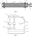
- FIG. 1 is a top view of an electro-optic modulator according to Embodiment 1 of the present invention.
- FIG. 2 is a schematic diagram of distribution of section layers of an electro-optic modulator according to Embodiment 1 of the present invention.
- the electro-optic modulator provided in this embodiment includes an input waveguide 11, a beam splitter 12 connected to the input waveguide 11, and a modulation arm that is disposed on each branch of the beam splitter 12 and that is configured to modulate a signal.
- a modulation arm that is disposed on each branch of the beam splitter 12 and that is configured to modulate a signal.
- the electro-optic modulator further includes a beam combiner 13 that is connected to each branch of the beam splitter 12 and that is configured to combine signals and an output waveguide 14 connected to the beam combiner 13.
- consecutive input optical signals enter the input waveguide 11 and are divided by the beam splitter 12 into two beams of light that have equal power, and the two beams of optical signals separately pass through the modulation arms and then are combined by the beam combiner 13 and finally output by the output waveguide 14.
- Each modulation arm is correspondingly disposed with a double-layer electrode
- a first layer electrode 21 of the double-layer electrode is a high-frequency traveling wave electrode (the "high-frequency traveling wave electrode” below is a first electrode 21) that is configured to change carrier concentration in the modulation arm
- a second layer electrode 26 is a direct current electrode having an inductor function, and there is an inductor connected to the high-frequency traveling wave electrode in an inductor formed in the second layer electrode 26.
- a to-be-modulated electrical signal is loaded onto the modulation arm by using the high-frequency traveling wave electrode.
- Carrier concentration in a modulation area waveguide of the modulation arm is changed, so that an effective refractive index of a modulation waveguide area is changed, and a phase difference between two beams of optical signals is dynamically changed to form modulation.
- the second layer electrode 26 is used as a direct current electrode, to implement the inductor function by using a threadlike metal cable design of the direct current electrode.
- the electro-optic modulator has some functions of a bias tee, integration of the electro-optic modulator is improved, and an external connection structure of the electro-optic modulator is reduced, so that the integration of the electro-optic modulator can be further improved without affecting performance of the electro-optic modulator, high-density packaging layout difficulty and cabling pressure can be effectively reduced, and cabling and packaging of a multi-channel high-speed signal on a base board can be implemented.
- two layers of electrode metal are further disposed at a modulator signal input end, to implement a function of a capacitor 24 by using an overlapping design.
- the capacitor 24 is disposed on a side of the input waveguide 11, the electro-optic modulator has a modulator high-frequency signal input end 33, one end of the capacitor 24 is connected to the modulator high-frequency signal input end 33 of the electro-optic modulator, the other end of the capacitor 24 is connected to the high-frequency traveling wave electrode, and the capacitor 24 and the inductor in the second layer electrode 26 are both connected to the high-frequency traveling wave electrode, to form a bias tee and load a high-frequency radio frequency signal and a direct current signal.
- the second layer electrode 26 includes a driver inductor 22 and a modulator inductor 23.
- the second layer electrode 26 of the electro-optic modulator provided in this embodiment includes a modulator inductor 23 corresponding to each modulation arm, one end of each modulator inductor 23 is connected to a modulator direct-current signal input end 31, and the other end is connected to the high-frequency traveling wave electrode.
- a direct current bias signal is input from the modulator direct-current signal input end 31 and is loaded onto the modulation arm by using the modulator inductor 23, to implement reverse biasing of a PN junction of the modulation arm.
- a to-be-modulated radio frequency electrical signal is input from the modulator high-frequency signal input end 33 and is loaded onto the modulation arm by using the capacitor 24.
- the carrier concentration in the modulation area waveguide is changed, so that an effective refractive index of the modulation area waveguide is changed, and a phase difference between two beams of optical signals is dynamically changed to form modulation.
- the electro-optic modulator further includes a thermal electrode 25 loaded onto each branch of the beam combiner 13.
- a direct current signal is loaded onto the thermal electrode 25, to change the effective refractive index of the waveguide area by using a thermo-optic effect, and control a phase bias point of the modulator.
- the second layer electrode 26 further includes a driver inductor 22 corresponding to each modulation arm.
- each driver inductor 22 is connected to a driver direct-current signal input end 32, and the other end of each driver inductor 22 is connected to the modulator high-frequency signal input end 33 of the electro-optic modulator.
- a direct current bias signal is input from the driver direct-current signal input end 32, passes through the driver inductor 22, and may be loaded onto a driver that provides a high-frequency radio frequency signal for the modulator, to provide a direct current voltage for the driver.
- FIG. 2 is a schematic diagram of distribution of section layers of an electro-optic modulator according to Embodiment 1 of the present invention. It can be learned from FIG. 2 that the electro-optic modulator provided in this embodiment has a silicon substrate 50, a buried silicon dioxide layer 60 disposed on the silicon substrate, and a modulator active-area silicon waveguide 80 and a silicon dioxide isolating layer 70 that are disposed on the buried silicon dioxide layer 60.
- the second layer electrode 26 is disposed on a side that is of the silicon dioxide isolating layer 70 and that is opposite to the buried silicon dioxide layer 60, the first layer electrode 21 is buried in the silicon dioxide isolating layer 70, and the first layer electrode 21 and the second layer electrode 26 are electrically connected.
- the silicon dioxide isolating layer 70 is disposed with a via hole, and the first layer electrode 21 and the second layer electrode 26 are connected by using metal filling the via hole.
- the first layer electrode 21 is connected to the modulator active-area silicon waveguide 80 by using the metal filling the via hole, and then connected to the second layer electrode 26 by using the metal in the via hole.
- An electrode of the capacitor 24 is disposed on the side that is of the silicon dioxide isolating layer 70 and that is opposite to the buried silicon dioxide layer 60, and the other electrode is buried in the silicon dioxide isolating layer 60.
- the electro-optic modulator uses a double-layer electrode structure, and implements functions of a high frequency electrode and the bias tee.
- first layer metal (the first layer electrode) of the electrode structure implements the high-frequency traveling wave electrode
- second layer metal (the second layer electrode) of the electrode structure implements the direct current electrode, to implement the inductor function by using the threadlike metal cable design of the direct current electrode.
- the two layers of electrode metal are disposed at the modulator signal input end, to implement the function of the capacitor 24 by using the overlapping design.
- the inductor and the capacitor 24 formed in the electrode structure are both connected to a radio frequency electrode of the modulator, to form a bias tee structure and load a high-frequency radio frequency signal and a direct current signal.
- high-density multi-channel integration of the modulator can be implemented in the present invention, can be compatible with a high-density packaging layout, and can implement high-speed high-density electro-packaging of a high-density multi-channel modulator.
- a bias tee is integrated in a modulator structure, so that the integration of the electro-optic modulator can be further improved without affecting performance of the electro-optic modulator, high-density packaging layout difficulty and cabling pressure can be effectively reduced, and cabling and packaging of a multi-channel high-speed signal on a base board can be implemented.
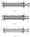
- FIG. 3 is a schematic structural diagram of an electro-optic modulator according to Embodiment 2 of the present invention.
- a second layer electrode includes only a modulator inductor 23.
- first layer metal of an electrode structure implements a high-frequency traveling wave electrode
- second layer metal of the electrode structure implements a direct current electrode, to implement an inductor function by using a threadlike metal cable design of the direct current electrode.
- Two layers of electrode metal at a modulator signal input end implement a function of a capacitor 24 by using an overlapping design.
- An inductor and the capacitor 24 formed in the electrode structure are both connected to a radio frequency electrode of the modulator, to form a bias tee structure and load a high-frequency radio frequency signal and a direct current signal.
- the modulator inductor 23 is connected to the radio frequency electrode, to provide a direct current voltage for the modulator.
- the integrated capacitor 24 is connected to both the modulator inductor 23 and a radio frequency input pad, to provide a radio frequency signal voltage for the modulator.
- FIG. 4 is a schematic structural diagram of an electro-optic modulator according to Embodiment 3 of the present invention. As shown in FIG. 4 , when Embodiment 3 is compared with Embodiment 1, a difference lies in that a second layer electrode in a double-layer electrode structure of the modulator includes a modulator inductor 23 and a driver inductor 22, and a capacitor 24 is omitted.
- first layer metal of the electrode structure implements a high-frequency traveling wave electrode
- second layer metal of the electrode structure implements a direct current electrode, to implement an inductor function by using a threadlike metal cable design of the direct current electrode.
- the modulator inductor 23 is connected to a radio frequency electrode, to provide a direct current voltage for the modulator.
- the driver inductor 22 provides a direct current voltage for a driver.
- FIG. 5 is a schematic structural diagram of an electro-optic modulator according to Embodiment 4 of the present invention. As shown in FIG. 5 , when Embodiment 4 is compared with Embodiment 1, a difference lies in that a second layer electrode in a double-layer electrode structure of the modulator includes only a modulator inductor 23, and a capacitor 24 and a driver inductor 22 are omitted.
- first layer metal of the electrode structure implements a high-frequency traveling wave electrode
- second layer metal of the electrode structure implements a direct current electrode, to implement an inductor function by using a threadlike metal cable design of the direct current electrode.
- the modulator inductor 23 is connected to a radio frequency electrode, to provide a direct current voltage for the modulator.
- the electro-optic modulator provided in the present invention uses a double-layer electrode structure, and a partial structure of a bias tee is integrated into the electro-optic modulator, or a double-layer electrode structure is set to form an inductor and a capacitor 24, to integrate an entire bias tee into the electro-optic modulator.
- high-density multi-channel integration of the modulator can be implemented in the present invention, can be compatible with a high-density packaging layout, and can implement high-speed high-density electro-packaging of a high-density multi-channel modulator.
- a bias tee is integrated in a modulator structure, so that integration of the electro-optic modulator can be further improved without affecting performance of the electro-optic modulator, high-density packaging layout difficulty and cabling pressure can be effectively reduced, and cabling and packaging of a multi-channel high-speed signal on a base board can be implemented.
- a technique of a double-layer electrode structure integrating the inductor and the capacitor 24 is compatible with a standard silicon photonics manufacturing technique, and the structure is compact and is extremely applicable to a high-density multi-channel high-capacity application scenario.
Landscapes
- Physics & Mathematics (AREA)
- Nonlinear Science (AREA)
- General Physics & Mathematics (AREA)
- Optics & Photonics (AREA)
- Optical Modulation, Optical Deflection, Nonlinear Optics, Optical Demodulation, Optical Logic Elements (AREA)
Applications Claiming Priority (1)
| Application Number | Priority Date | Filing Date | Title |
|---|---|---|---|
| PCT/CN2016/090890 WO2018014302A1 (fr) | 2016-07-21 | 2016-07-21 | Modulateur électro-optique |
Publications (3)
| Publication Number | Publication Date |
|---|---|
| EP3477362A1 true EP3477362A1 (fr) | 2019-05-01 |
| EP3477362A4 EP3477362A4 (fr) | 2019-06-26 |
| EP3477362B1 EP3477362B1 (fr) | 2022-01-12 |
Family
ID=60992784
Family Applications (1)
| Application Number | Title | Priority Date | Filing Date |
|---|---|---|---|
| EP16909229.3A Active EP3477362B1 (fr) | 2016-07-21 | 2016-07-21 | Modulateur électro-optique |
Country Status (4)
| Country | Link |
|---|---|
| US (1) | US10684497B2 (fr) |
| EP (1) | EP3477362B1 (fr) |
| CN (1) | CN108780234B (fr) |
| WO (1) | WO2018014302A1 (fr) |
Cited By (6)
| Publication number | Priority date | Publication date | Assignee | Title |
|---|---|---|---|---|
| WO2021226395A1 (fr) * | 2020-05-06 | 2021-11-11 | The Trustees Of The Stevens Institute Of Technology | Dispositifs et procédés de modulation optique à basse tension |
| US11968298B2 (en) | 2019-10-18 | 2024-04-23 | The Trustees Of The Stevens Institute Of Technology | Systems and methods for quantum-secured, private-preserving computations |
| US12455355B2 (en) | 2018-06-13 | 2025-10-28 | The Trustees Of The Stevens Institute Of Technology | Approaches, apparatuses and methods for LIDAR applications based on-mode-selective frequency conversion |
| US12517039B2 (en) | 2021-09-14 | 2026-01-06 | The Trustees Of The Stevens Institute Of Technology | System and methods for gas spectroscopic sensing with photon counting and tunable integrated photonic filters |
| US12523915B2 (en) | 2020-05-13 | 2026-01-13 | The Trustees Of The Stevens Institute Of Technology | Super ising emulator with multi-body interactions and all-to-all connections |
| US12596028B2 (en) | 2021-08-30 | 2026-04-07 | The Trustees Of The Stevens Institute Of Technology | Method and system for non-interferometric quantum photonics vibrometry |
Families Citing this family (3)
| Publication number | Priority date | Publication date | Assignee | Title |
|---|---|---|---|---|
| CN115149395A (zh) * | 2022-06-30 | 2022-10-04 | 杰创半导体(苏州)有限公司 | 光通信集成芯片及其制作方法 |
| CN115728883B (zh) * | 2022-11-16 | 2025-08-05 | 中国科学院微电子研究所 | 一种三维光电封装结构和封装方法 |
| CN118688985B (zh) * | 2024-08-28 | 2025-02-25 | 易栅光电(杭州)有限公司 | 一种用于高速光通信和光计算的可见光调制器 |
Family Cites Families (12)
| Publication number | Priority date | Publication date | Assignee | Title |
|---|---|---|---|---|
| JPH11237593A (ja) * | 1998-02-20 | 1999-08-31 | Sumitomo Osaka Cement Co Ltd | 光変調器 |
| GB2375614B (en) * | 2000-04-06 | 2003-07-16 | Bookham Technology Plc | Optical modulator with pre-determined frequency chirp |
| JP3936256B2 (ja) * | 2002-07-18 | 2007-06-27 | 富士通株式会社 | 光半導体装置 |
| US7127128B2 (en) * | 2005-03-03 | 2006-10-24 | Avanex Corporation | Electro-optical device |
| JP4110182B2 (ja) * | 2006-09-30 | 2008-07-02 | 住友大阪セメント株式会社 | 光制御素子 |
| US7529433B2 (en) * | 2007-01-12 | 2009-05-05 | Jds Uniphase Corporation | Humidity tolerant electro-optic device |
| JP2012108238A (ja) * | 2010-11-16 | 2012-06-07 | Mitsubishi Electric Corp | 光変調装置 |
| JP5291764B2 (ja) * | 2011-06-24 | 2013-09-18 | 株式会社アドバンテスト | 光デバイスおよび光変調装置 |
| JP5690366B2 (ja) | 2013-03-26 | 2015-03-25 | 住友大阪セメント株式会社 | 光変調器 |
| CN105044931B (zh) * | 2015-09-10 | 2018-10-09 | 中国科学院半导体研究所 | 硅基集成化的差分电光调制器及其制备方法 |
| JP2018105975A (ja) * | 2016-12-26 | 2018-07-05 | 株式会社フジクラ | 光変調素子 |
| CN206759461U (zh) * | 2017-03-20 | 2017-12-15 | 上海交通大学 | 单边带电光调制装置 |
-
2016
- 2016-07-21 WO PCT/CN2016/090890 patent/WO2018014302A1/fr not_active Ceased
- 2016-07-21 CN CN201680081996.0A patent/CN108780234B/zh active Active
- 2016-07-21 EP EP16909229.3A patent/EP3477362B1/fr active Active
-
2019
- 2019-01-18 US US16/252,450 patent/US10684497B2/en active Active
Cited By (7)
| Publication number | Priority date | Publication date | Assignee | Title |
|---|---|---|---|---|
| US12455355B2 (en) | 2018-06-13 | 2025-10-28 | The Trustees Of The Stevens Institute Of Technology | Approaches, apparatuses and methods for LIDAR applications based on-mode-selective frequency conversion |
| US11968298B2 (en) | 2019-10-18 | 2024-04-23 | The Trustees Of The Stevens Institute Of Technology | Systems and methods for quantum-secured, private-preserving computations |
| WO2021226395A1 (fr) * | 2020-05-06 | 2021-11-11 | The Trustees Of The Stevens Institute Of Technology | Dispositifs et procédés de modulation optique à basse tension |
| US12292626B2 (en) | 2020-05-06 | 2025-05-06 | The Trustees Of The Stevens Institute Of Technology | Devices and methods for low voltage optical modulation |
| US12523915B2 (en) | 2020-05-13 | 2026-01-13 | The Trustees Of The Stevens Institute Of Technology | Super ising emulator with multi-body interactions and all-to-all connections |
| US12596028B2 (en) | 2021-08-30 | 2026-04-07 | The Trustees Of The Stevens Institute Of Technology | Method and system for non-interferometric quantum photonics vibrometry |
| US12517039B2 (en) | 2021-09-14 | 2026-01-06 | The Trustees Of The Stevens Institute Of Technology | System and methods for gas spectroscopic sensing with photon counting and tunable integrated photonic filters |
Also Published As
| Publication number | Publication date |
|---|---|
| CN108780234B (zh) | 2021-04-20 |
| US10684497B2 (en) | 2020-06-16 |
| WO2018014302A1 (fr) | 2018-01-25 |
| CN108780234A (zh) | 2018-11-09 |
| EP3477362A4 (fr) | 2019-06-26 |
| EP3477362B1 (fr) | 2022-01-12 |
| US20190171044A1 (en) | 2019-06-06 |
Similar Documents
| Publication | Publication Date | Title |
|---|---|---|
| US10684497B2 (en) | Electro-optic modulator | |
| CN113540063B (zh) | 兼容锗硅探测器和薄膜铌酸锂调制器的硅光集成芯片 | |
| CN105044931B (zh) | 硅基集成化的差分电光调制器及其制备方法 | |
| KR101561368B1 (ko) | 광 도파관 구조 | |
| US8300990B2 (en) | Slotted optical waveguide with electro-optic material | |
| US8969989B2 (en) | Optical-to-electrical converter unit and semiconductor light-receiving device | |
| US20190129273A1 (en) | Optical modulator | |
| US20250199375A1 (en) | Electro-optical modulator and manufacturing method thereof | |
| CN111273464B (zh) | 基于铌酸锂-硅晶圆的光电单片集成系统 | |
| WO2021142588A1 (fr) | Modulateur électro-optique et son procédé de fabrication et puce | |
| JP2023527091A5 (fr) | ||
| JP2023527091A (ja) | 電気光変調器、光チップ及び集積チップ | |
| CN102044844B (zh) | 分布放大的取样光栅分布布拉格反射可调谐激光器 | |
| US10326423B1 (en) | Impedance matching circuits for photonic devices | |
| US8805126B2 (en) | Photonic modulator with forward-and reverse-biased diodes for separate tuning and modulating elements | |
| US11156858B2 (en) | Optical device that includes optical modulator | |
| US12292625B2 (en) | Building block for electro-optical integrated indium-phosphide based phase modulator | |
| CN113900282A (zh) | 一种硅基集成宽带高速可调谐微波光子移相器芯片 | |
| CN118838076A (zh) | 硅光调制器及光电器件 | |
| WO2021223633A1 (fr) | Modulateur électro-optique, circuit de modulation électro-optique et dispositif de communication optique | |
| JP7830650B2 (ja) | チップ及び光通信デバイス | |
| US20250172831A1 (en) | Electro-optical modulators integrated with photodiodes | |
| US20250172848A1 (en) | Optical device, transmitter, and transceiver | |
| Kaiser et al. | Monolithic flip-chip compatible twin-IQ Mach-Zehnder modulators for hybrid assembly onto high capacity optical transmitter boards | |
| US20240379644A1 (en) | Optical Communication Device |
Legal Events
| Date | Code | Title | Description |
|---|---|---|---|
| STAA | Information on the status of an ep patent application or granted ep patent |
Free format text: STATUS: THE INTERNATIONAL PUBLICATION HAS BEEN MADE |
|
| PUAI | Public reference made under article 153(3) epc to a published international application that has entered the european phase |
Free format text: ORIGINAL CODE: 0009012 |
|
| STAA | Information on the status of an ep patent application or granted ep patent |
Free format text: STATUS: REQUEST FOR EXAMINATION WAS MADE |
|
| 17P | Request for examination filed |
Effective date: 20190124 |
|
| AK | Designated contracting states |
Kind code of ref document: A1 Designated state(s): AL AT BE BG CH CY CZ DE DK EE ES FI FR GB GR HR HU IE IS IT LI LT LU LV MC MK MT NL NO PL PT RO RS SE SI SK SM TR |
|
| AX | Request for extension of the european patent |
Extension state: BA ME |
|
| A4 | Supplementary search report drawn up and despatched |
Effective date: 20190529 |
|
| RIC1 | Information provided on ipc code assigned before grant |
Ipc: G02F 1/015 20060101AFI20190523BHEP |
|
| DAV | Request for validation of the european patent (deleted) | ||
| DAX | Request for extension of the european patent (deleted) | ||
| GRAP | Despatch of communication of intention to grant a patent |
Free format text: ORIGINAL CODE: EPIDOSNIGR1 |
|
| STAA | Information on the status of an ep patent application or granted ep patent |
Free format text: STATUS: GRANT OF PATENT IS INTENDED |
|
| GRAJ | Information related to disapproval of communication of intention to grant by the applicant or resumption of examination proceedings by the epo deleted |
Free format text: ORIGINAL CODE: EPIDOSDIGR1 |
|
| GRAP | Despatch of communication of intention to grant a patent |
Free format text: ORIGINAL CODE: EPIDOSNIGR1 |
|
| INTG | Intention to grant announced |
Effective date: 20210722 |
|
| RIN1 | Information on inventor provided before grant (corrected) |
Inventor name: LI, YANBO Inventor name: SONG, XIAOLU Inventor name: DONG, ZHEN Inventor name: JI, RUIQIANG Inventor name: FU, SHENGMENG Inventor name: ZENG, LI |
|
| INTG | Intention to grant announced |
Effective date: 20210810 |
|
| GRAS | Grant fee paid |
Free format text: ORIGINAL CODE: EPIDOSNIGR3 |
|
| GRAA | (expected) grant |
Free format text: ORIGINAL CODE: 0009210 |
|
| STAA | Information on the status of an ep patent application or granted ep patent |
Free format text: STATUS: THE PATENT HAS BEEN GRANTED |
|
| AK | Designated contracting states |
Kind code of ref document: B1 Designated state(s): AL AT BE BG CH CY CZ DE DK EE ES FI FR GB GR HR HU IE IS IT LI LT LU LV MC MK MT NL NO PL PT RO RS SE SI SK SM TR |
|
| REG | Reference to a national code |
Ref country code: GB Ref legal event code: FG4D |
|
| REG | Reference to a national code |
Ref country code: CH Ref legal event code: EP |
|
| REG | Reference to a national code |
Ref country code: DE Ref legal event code: R096 Ref document number: 602016068407 Country of ref document: DE |
|
| REG | Reference to a national code |
Ref country code: IE Ref legal event code: FG4D |
|
| REG | Reference to a national code |
Ref country code: AT Ref legal event code: REF Ref document number: 1462773 Country of ref document: AT Kind code of ref document: T Effective date: 20220215 |
|
| REG | Reference to a national code |
Ref country code: LT Ref legal event code: MG9D |
|
| REG | Reference to a national code |
Ref country code: NL Ref legal event code: MP Effective date: 20220112 |
|
| REG | Reference to a national code |
Ref country code: AT Ref legal event code: MK05 Ref document number: 1462773 Country of ref document: AT Kind code of ref document: T Effective date: 20220112 |
|
| PG25 | Lapsed in a contracting state [announced via postgrant information from national office to epo] |
Ref country code: NL Free format text: LAPSE BECAUSE OF FAILURE TO SUBMIT A TRANSLATION OF THE DESCRIPTION OR TO PAY THE FEE WITHIN THE PRESCRIBED TIME-LIMIT Effective date: 20220112 |
|
| PG25 | Lapsed in a contracting state [announced via postgrant information from national office to epo] |
Ref country code: SE Free format text: LAPSE BECAUSE OF FAILURE TO SUBMIT A TRANSLATION OF THE DESCRIPTION OR TO PAY THE FEE WITHIN THE PRESCRIBED TIME-LIMIT Effective date: 20220112 Ref country code: RS Free format text: LAPSE BECAUSE OF FAILURE TO SUBMIT A TRANSLATION OF THE DESCRIPTION OR TO PAY THE FEE WITHIN THE PRESCRIBED TIME-LIMIT Effective date: 20220112 Ref country code: PT Free format text: LAPSE BECAUSE OF FAILURE TO SUBMIT A TRANSLATION OF THE DESCRIPTION OR TO PAY THE FEE WITHIN THE PRESCRIBED TIME-LIMIT Effective date: 20220512 Ref country code: NO Free format text: LAPSE BECAUSE OF FAILURE TO SUBMIT A TRANSLATION OF THE DESCRIPTION OR TO PAY THE FEE WITHIN THE PRESCRIBED TIME-LIMIT Effective date: 20220412 Ref country code: LT Free format text: LAPSE BECAUSE OF FAILURE TO SUBMIT A TRANSLATION OF THE DESCRIPTION OR TO PAY THE FEE WITHIN THE PRESCRIBED TIME-LIMIT Effective date: 20220112 Ref country code: HR Free format text: LAPSE BECAUSE OF FAILURE TO SUBMIT A TRANSLATION OF THE DESCRIPTION OR TO PAY THE FEE WITHIN THE PRESCRIBED TIME-LIMIT Effective date: 20220112 Ref country code: ES Free format text: LAPSE BECAUSE OF FAILURE TO SUBMIT A TRANSLATION OF THE DESCRIPTION OR TO PAY THE FEE WITHIN THE PRESCRIBED TIME-LIMIT Effective date: 20220112 Ref country code: BG Free format text: LAPSE BECAUSE OF FAILURE TO SUBMIT A TRANSLATION OF THE DESCRIPTION OR TO PAY THE FEE WITHIN THE PRESCRIBED TIME-LIMIT Effective date: 20220412 |
|
| PG25 | Lapsed in a contracting state [announced via postgrant information from national office to epo] |
Ref country code: PL Free format text: LAPSE BECAUSE OF FAILURE TO SUBMIT A TRANSLATION OF THE DESCRIPTION OR TO PAY THE FEE WITHIN THE PRESCRIBED TIME-LIMIT Effective date: 20220112 Ref country code: LV Free format text: LAPSE BECAUSE OF FAILURE TO SUBMIT A TRANSLATION OF THE DESCRIPTION OR TO PAY THE FEE WITHIN THE PRESCRIBED TIME-LIMIT Effective date: 20220112 Ref country code: GR Free format text: LAPSE BECAUSE OF FAILURE TO SUBMIT A TRANSLATION OF THE DESCRIPTION OR TO PAY THE FEE WITHIN THE PRESCRIBED TIME-LIMIT Effective date: 20220413 Ref country code: FI Free format text: LAPSE BECAUSE OF FAILURE TO SUBMIT A TRANSLATION OF THE DESCRIPTION OR TO PAY THE FEE WITHIN THE PRESCRIBED TIME-LIMIT Effective date: 20220112 Ref country code: AT Free format text: LAPSE BECAUSE OF FAILURE TO SUBMIT A TRANSLATION OF THE DESCRIPTION OR TO PAY THE FEE WITHIN THE PRESCRIBED TIME-LIMIT Effective date: 20220112 |
|
| PG25 | Lapsed in a contracting state [announced via postgrant information from national office to epo] |
Ref country code: IS Free format text: LAPSE BECAUSE OF FAILURE TO SUBMIT A TRANSLATION OF THE DESCRIPTION OR TO PAY THE FEE WITHIN THE PRESCRIBED TIME-LIMIT Effective date: 20220512 |
|
| REG | Reference to a national code |
Ref country code: DE Ref legal event code: R097 Ref document number: 602016068407 Country of ref document: DE |
|
| PG25 | Lapsed in a contracting state [announced via postgrant information from national office to epo] |
Ref country code: SM Free format text: LAPSE BECAUSE OF FAILURE TO SUBMIT A TRANSLATION OF THE DESCRIPTION OR TO PAY THE FEE WITHIN THE PRESCRIBED TIME-LIMIT Effective date: 20220112 Ref country code: SK Free format text: LAPSE BECAUSE OF FAILURE TO SUBMIT A TRANSLATION OF THE DESCRIPTION OR TO PAY THE FEE WITHIN THE PRESCRIBED TIME-LIMIT Effective date: 20220112 Ref country code: RO Free format text: LAPSE BECAUSE OF FAILURE TO SUBMIT A TRANSLATION OF THE DESCRIPTION OR TO PAY THE FEE WITHIN THE PRESCRIBED TIME-LIMIT Effective date: 20220112 Ref country code: EE Free format text: LAPSE BECAUSE OF FAILURE TO SUBMIT A TRANSLATION OF THE DESCRIPTION OR TO PAY THE FEE WITHIN THE PRESCRIBED TIME-LIMIT Effective date: 20220112 Ref country code: DK Free format text: LAPSE BECAUSE OF FAILURE TO SUBMIT A TRANSLATION OF THE DESCRIPTION OR TO PAY THE FEE WITHIN THE PRESCRIBED TIME-LIMIT Effective date: 20220112 Ref country code: CZ Free format text: LAPSE BECAUSE OF FAILURE TO SUBMIT A TRANSLATION OF THE DESCRIPTION OR TO PAY THE FEE WITHIN THE PRESCRIBED TIME-LIMIT Effective date: 20220112 |
|
| PLBE | No opposition filed within time limit |
Free format text: ORIGINAL CODE: 0009261 |
|
| STAA | Information on the status of an ep patent application or granted ep patent |
Free format text: STATUS: NO OPPOSITION FILED WITHIN TIME LIMIT |
|
| PG25 | Lapsed in a contracting state [announced via postgrant information from national office to epo] |
Ref country code: AL Free format text: LAPSE BECAUSE OF FAILURE TO SUBMIT A TRANSLATION OF THE DESCRIPTION OR TO PAY THE FEE WITHIN THE PRESCRIBED TIME-LIMIT Effective date: 20220112 |
|
| 26N | No opposition filed |
Effective date: 20221013 |
|
| PG25 | Lapsed in a contracting state [announced via postgrant information from national office to epo] |
Ref country code: SI Free format text: LAPSE BECAUSE OF FAILURE TO SUBMIT A TRANSLATION OF THE DESCRIPTION OR TO PAY THE FEE WITHIN THE PRESCRIBED TIME-LIMIT Effective date: 20220112 Ref country code: MC Free format text: LAPSE BECAUSE OF FAILURE TO SUBMIT A TRANSLATION OF THE DESCRIPTION OR TO PAY THE FEE WITHIN THE PRESCRIBED TIME-LIMIT Effective date: 20220112 |
|
| REG | Reference to a national code |
Ref country code: CH Ref legal event code: PL |
|
| REG | Reference to a national code |
Ref country code: BE Ref legal event code: MM Effective date: 20220731 |
|
| PG25 | Lapsed in a contracting state [announced via postgrant information from national office to epo] |
Ref country code: LU Free format text: LAPSE BECAUSE OF NON-PAYMENT OF DUE FEES Effective date: 20220721 Ref country code: LI Free format text: LAPSE BECAUSE OF NON-PAYMENT OF DUE FEES Effective date: 20220731 Ref country code: FR Free format text: LAPSE BECAUSE OF NON-PAYMENT OF DUE FEES Effective date: 20220731 Ref country code: CH Free format text: LAPSE BECAUSE OF NON-PAYMENT OF DUE FEES Effective date: 20220731 |
|
| PG25 | Lapsed in a contracting state [announced via postgrant information from national office to epo] |
Ref country code: BE Free format text: LAPSE BECAUSE OF NON-PAYMENT OF DUE FEES Effective date: 20220731 |
|
| PG25 | Lapsed in a contracting state [announced via postgrant information from national office to epo] |
Ref country code: IT Free format text: LAPSE BECAUSE OF FAILURE TO SUBMIT A TRANSLATION OF THE DESCRIPTION OR TO PAY THE FEE WITHIN THE PRESCRIBED TIME-LIMIT Effective date: 20220112 Ref country code: IE Free format text: LAPSE BECAUSE OF NON-PAYMENT OF DUE FEES Effective date: 20220721 |
|
| PG25 | Lapsed in a contracting state [announced via postgrant information from national office to epo] |
Ref country code: HU Free format text: LAPSE BECAUSE OF FAILURE TO SUBMIT A TRANSLATION OF THE DESCRIPTION OR TO PAY THE FEE WITHIN THE PRESCRIBED TIME-LIMIT; INVALID AB INITIO Effective date: 20160721 |
|
| PG25 | Lapsed in a contracting state [announced via postgrant information from national office to epo] |
Ref country code: MK Free format text: LAPSE BECAUSE OF FAILURE TO SUBMIT A TRANSLATION OF THE DESCRIPTION OR TO PAY THE FEE WITHIN THE PRESCRIBED TIME-LIMIT Effective date: 20220112 Ref country code: CY Free format text: LAPSE BECAUSE OF FAILURE TO SUBMIT A TRANSLATION OF THE DESCRIPTION OR TO PAY THE FEE WITHIN THE PRESCRIBED TIME-LIMIT Effective date: 20220112 |
|
| PG25 | Lapsed in a contracting state [announced via postgrant information from national office to epo] |
Ref country code: TR Free format text: LAPSE BECAUSE OF FAILURE TO SUBMIT A TRANSLATION OF THE DESCRIPTION OR TO PAY THE FEE WITHIN THE PRESCRIBED TIME-LIMIT Effective date: 20220112 |
|
| PG25 | Lapsed in a contracting state [announced via postgrant information from national office to epo] |
Ref country code: MT Free format text: LAPSE BECAUSE OF FAILURE TO SUBMIT A TRANSLATION OF THE DESCRIPTION OR TO PAY THE FEE WITHIN THE PRESCRIBED TIME-LIMIT Effective date: 20220112 |
|
| PGFP | Annual fee paid to national office [announced via postgrant information from national office to epo] |
Ref country code: GB Payment date: 20250529 Year of fee payment: 10 |
|
| PGFP | Annual fee paid to national office [announced via postgrant information from national office to epo] |
Ref country code: DE Payment date: 20250604 Year of fee payment: 10 |